Dr. Khaldoon N. Abbas Electronics II/ 3 rd Grade Physics Dep. College of Science 1 Chapter (2) Field-Effect Transistor (FET) 2.1 Introduction The field effect transistor (FET) is a semiconductor device whose operation consists of controlling the flow of current through a semiconductor channel by applies of an electric field (voltage). Usually, a field effect transistor (FET) is a three-terminal semiconductor device (Figures 2-1a-b), in which current conduction is via one type of charge carriers (electrons or holes). Unlike the usual transistor, the flow of current is controlled by means of an electric field (controlled by the effect of the electric field) developed between the gate electrode (g) and the conducting channel of the device. There are two types of FETs: (a) Junction field effect transistors (JFET). (b) Metal-oxide semiconductor field effect transistor (MOSFET). These two types of FETs will be introduced in this chapter. Both types of FETs are categorized to n-channel or p-channel depending on their constructions. Furthermore, the MOSFET type is further categorized into depletion and enhancement types.

Welcome message from author
This document is posted to help you gain knowledge. Please leave a comment to let me know what you think about it! Share it to your friends and learn new things together.
Transcript

Dr. Khaldoon N. Abbas Electronics II/ 3rd Grade Physics Dep. College of Science
1
Chapter (2)
Field-Effect Transistor (FET)
2.1 Introduction
The field effect transistor (FET) is a semiconductor device whose operation
consists of controlling the flow of current through a semiconductor channel by
applies of an electric field (voltage). Usually, a field effect transistor (FET) is a
three-terminal semiconductor device (Figures 2-1a-b), in which current conduction
is via one type of charge carriers (electrons or holes). Unlike the usual transistor,
the flow of current is controlled by means of an electric field (controlled by the
effect of the electric field) developed between the gate electrode (g) and the
conducting channel of the device.
There are two types of FETs:
(a) Junction field effect transistors (JFET).
(b) Metal-oxide semiconductor field effect transistor (MOSFET).
These two types of FETs will be introduced in this chapter. Both types of FETs
are categorized to n-channel or p-channel depending on their constructions.
Furthermore, the MOSFET type is further categorized into depletion and
enhancement types.
Dr. Khaldoon N. Abbas Electronics II/ 3rd Grade Physics Dep. College of Science
2
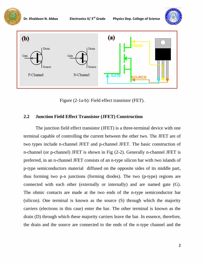
Figure (2-1a-b): Field effect transistor (FET).
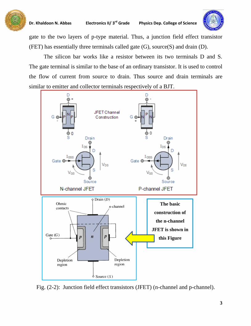
2.2 Junction Field Effect Transistor (JFET) Construction
The junction field effect transistor (JFET) is a three-terminal device with one
terminal capable of controlling the current between the other two. The JFET are of
two types include n-channel JFET and p-channel JFET. The basic construction of
n-channel (or p-channel) JFET is shown in Fig (2-2). Generally n-channel JFET is
preferred, in an n-channel JFET consists of an n-type silicon bar with two islands of
p-type semiconductors material diffused on the opposite sides of its middle part,
thus forming two p-n junctions (forming diodes). The two (p-type) regions are
connected with each other (externally or internally) and are named gate (G).
The ohmic contacts are made at the two ends of the n-type semiconductor bar
(silicon). One terminal is known as the source (S) through which the majority
carriers (electrons in this case) enter the bar. The other terminal is known as the
drain (D) through which these majority carriers leave the bar. In essence, therefore,
the drain and the source are connected to the ends of the n-type channel and the
Dr. Khaldoon N. Abbas Electronics II/ 3rd Grade Physics Dep. College of Science
3
gate to the two layers of p-type material. Thus, a junction field effect transistor
(FET) has essentially three terminals called gate (G), source(S) and drain (D).
The silicon bar works like a resistor between its two terminals D and S.
The gate terminal is similar to the base of an ordinary transistor. It is used to control
the flow of current from source to drain. Thus source and drain terminals are
similar to emitter and collector terminals respectively of a BJT.
Fig. (2-2): Junction field effect transistors (JFET) (n-channel and p-channel).
The basic
construction of
the n-channel
JFET is shown in
this Figure
Dr. Khaldoon N. Abbas Electronics II/ 3rd Grade Physics Dep. College of Science
4
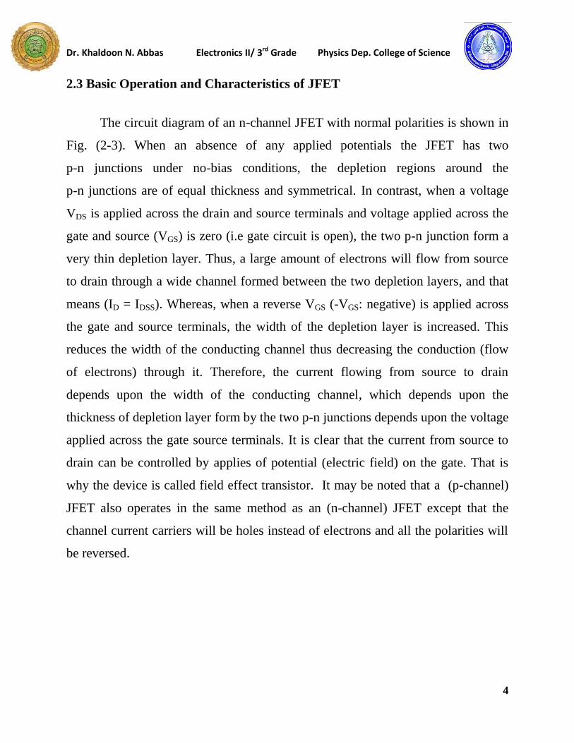
2.3 Basic Operation and Characteristics of JFET
The circuit diagram of an n-channel JFET with normal polarities is shown in
Fig. (2-3). When an absence of any applied potentials the JFET has two
p-n junctions under no-bias conditions, the depletion regions around the
p-n junctions are of equal thickness and symmetrical. In contrast, when a voltage
VDS is applied across the drain and source terminals and voltage applied across the
gate and source (VGS) is zero (i.e gate circuit is open), the two p-n junction form a
very thin depletion layer. Thus, a large amount of electrons will flow from source
to drain through a wide channel formed between the two depletion layers, and that
means (ID = IDSS). Whereas, when a reverse VGS (-VGS: negative) is applied across
the gate and source terminals, the width of the depletion layer is increased. This
reduces the width of the conducting channel thus decreasing the conduction (flow
of electrons) through it. Therefore, the current flowing from source to drain
depends upon the width of the conducting channel, which depends upon the
thickness of depletion layer form by the two p-n junctions depends upon the voltage
applied across the gate source terminals. It is clear that the current from source to
drain can be controlled by applies of potential (electric field) on the gate. That is
why the device is called field effect transistor. It may be noted that a (p-channel)
JFET also operates in the same method as an (n-channel) JFET except that the
channel current carriers will be holes instead of electrons and all the polarities will
be reversed.
Dr. Khaldoon N. Abbas Electronics II/ 3rd Grade Physics Dep. College of Science
5
Fig. (2-3): The circuit diagram of an n- channel JFET.
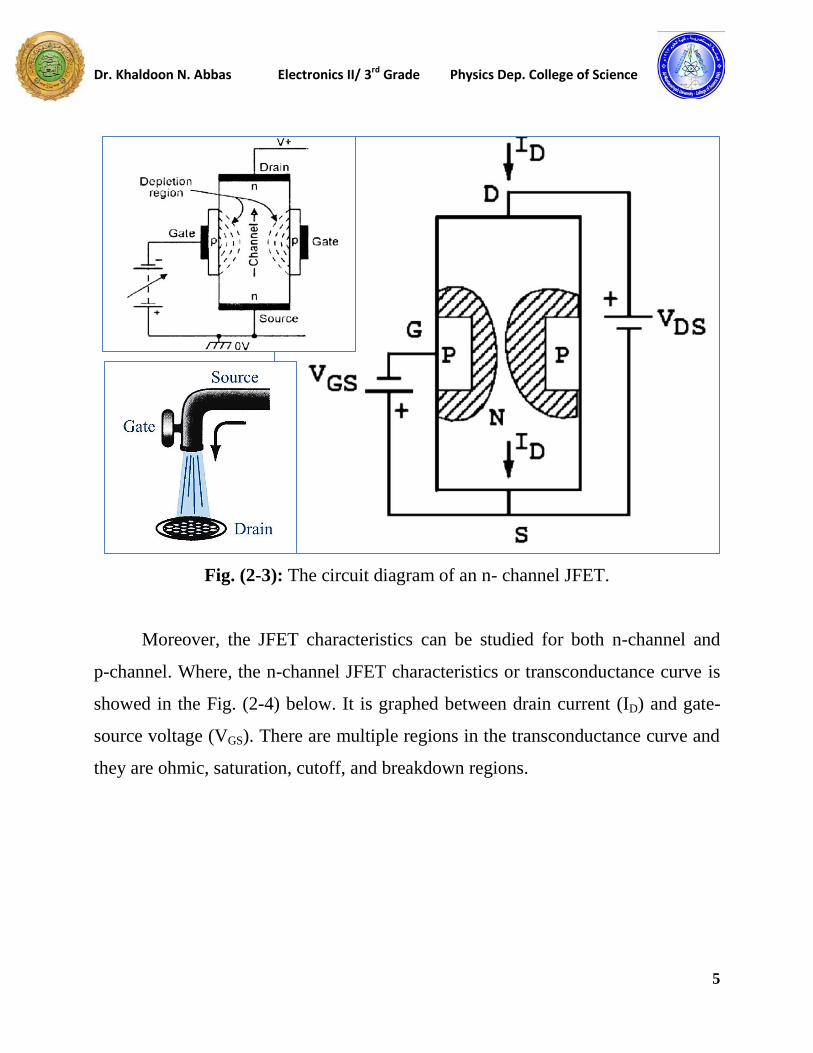
Moreover, the JFET characteristics can be studied for both n-channel and
p-channel. Where, the n-channel JFET characteristics or transconductance curve is
showed in the Fig. (2-4) below. It is graphed between drain current (ID) and gate-
source voltage (VGS). There are multiple regions in the transconductance curve and
they are ohmic, saturation, cutoff, and breakdown regions.
Dr. Khaldoon N. Abbas Electronics II/ 3rd Grade Physics Dep. College of Science
6
Fig. (2-4): (I-V) Characteristics of n-channel JFET, where for the n-channel device
the controlling voltage VGS is made more and more negative from its VGS = 0 V
level. In other words, the gate terminal will be set at lower and lower potential
levels as compared to the source.
2.4 Metal Oxide Semiconductor Field Effect (MOSFET)
The Metal Oxide Semiconductor Field Effect Transistor (MOSFET) is one
type of FET transistor. MOSFET is further categorized into depletion and
enhancement types. Usually, the (MOSFET) is a three terminal semiconductor
device. There are three terminals include source (S), gate (G) and drain (D). Unlike
a JFET, in this device the gate is electrically insulated from the current carrying
channel therefore sometimes it is also known as insulated gate FET (IGFET).
Dr. Khaldoon N. Abbas Electronics II/ 3rd Grade Physics Dep. College of Science
7
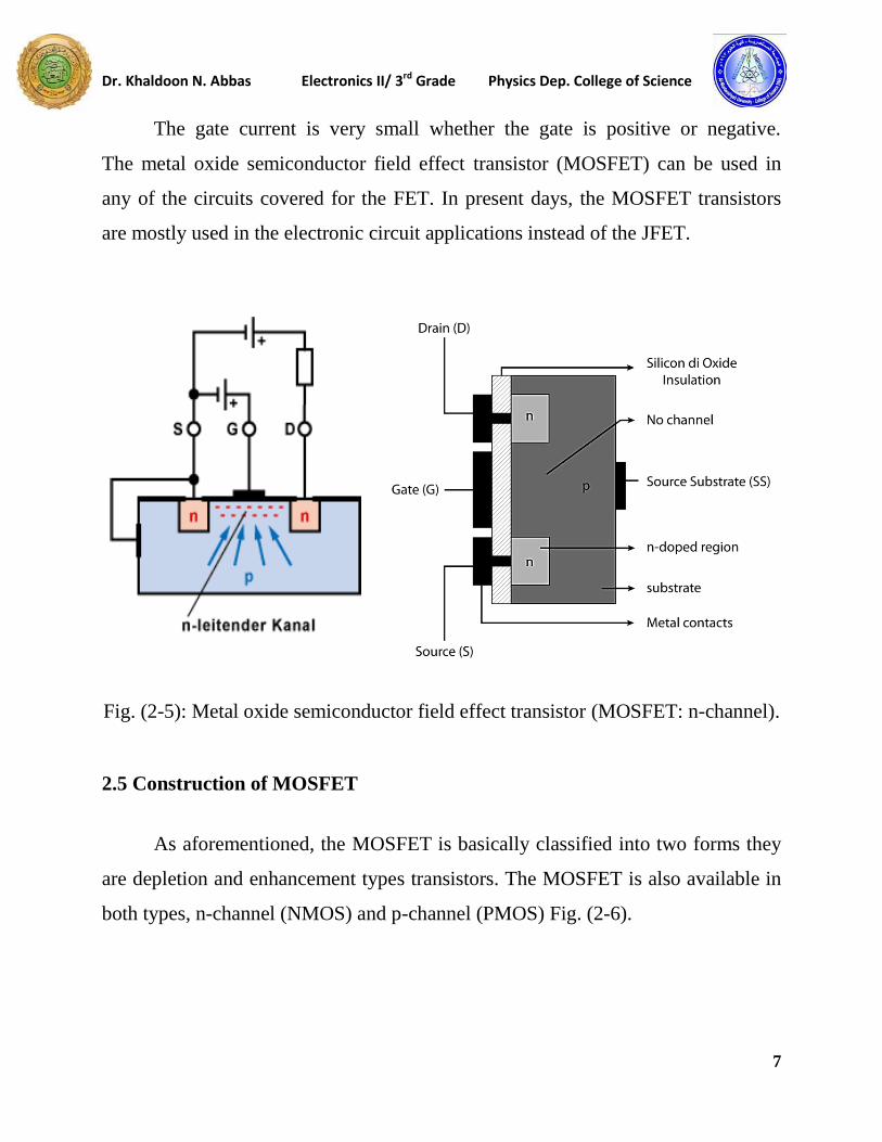
The gate current is very small whether the gate is positive or negative.
The metal oxide semiconductor field effect transistor (MOSFET) can be used in
any of the circuits covered for the FET. In present days, the MOSFET transistors
are mostly used in the electronic circuit applications instead of the JFET.
Fig. (2-5): Metal oxide semiconductor field effect transistor (MOSFET: n-channel).
2.5 Construction of MOSFET
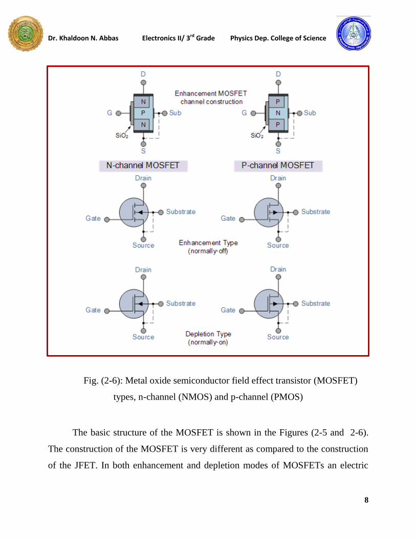
As aforementioned, the MOSFET is basically classified into two forms they
are depletion and enhancement types transistors. The MOSFET is also available in
both types, n-channel (NMOS) and p-channel (PMOS) Fig. (2-6).
Dr. Khaldoon N. Abbas Electronics II/ 3rd Grade Physics Dep. College of Science
8
Fig. (2-6): Metal oxide semiconductor field effect transistor (MOSFET)
types, n-channel (NMOS) and p-channel (PMOS)
The basic structure of the MOSFET is shown in the Figures (2-5 and 2-6).
The construction of the MOSFET is very different as compared to the construction
of the JFET. In both enhancement and depletion modes of MOSFETs an electric
Dr. Khaldoon N. Abbas Electronics II/ 3rd Grade Physics Dep. College of Science
9
field is produced by gate voltage which changes the flow charge carriers, such as
electrons for n-channel and holes for p-channel.
The simple side view of an n-channel MOSFET is shown in Fig. (2-6) left
the figure shows its constructional details. The source (S) and drain (D) terminals
are connected through metallic contacts to n-doped regions linked by an n-channel
as shown in the Figures (2-5 and 2-6). The gate (G) is also connected to a metal
contact surface but remains insulated from the n-channel by a very thin layer
usually silicon dioxide SiO2. The fact that the deposited SiO2 layer is an insulating
layer reveals that there is no direct electrical connection between the gate (G)
terminal and the channel of a MOSFET. The input impedance of MOSFET is very
high (of the order of 10^10
to 10^15
ohms).
2.5 Basic Operation and Characteristics of MOSFET
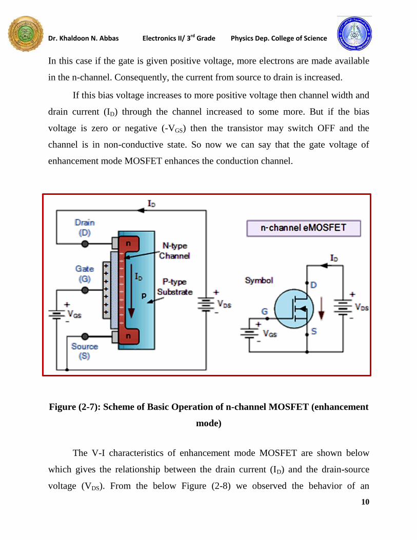
The Enhancement mode MOSFET is commonly used type of transistor.
This type of MOSFET is equivalent to normally-open switch because it does not
conduct when the gate (G) voltage is zero. The circuit diagram of an n-channel
MOSFET (Enhancement mode, EMOSFET) with normal polarities is shown in the
Figure (2-7). When negative voltage (-VGS) is applied to the gate (G), electrons
accumulate on it. These electrons repel or (prevent) the conduction hand electrons
in the n-channel. Therefore the number of conduction electrons available for
current conduction through the channel will reduce. Thus, the greater the negative
potential on the gate, the lesser is the current conduction from source to drain.
In contrast, if the positive voltage (+VGS) is applied to the n-channel gate terminal,
then the channel conducts and the drain current flows through the channel.
Dr. Khaldoon N. Abbas Electronics II/ 3rd Grade Physics Dep. College of Science
10
In this case if the gate is given positive voltage, more electrons are made available
in the n-channel. Consequently, the current from source to drain is increased.
If this bias voltage increases to more positive voltage then channel width and
drain current (ID) through the channel increased to some more. But if the bias
voltage is zero or negative (-VGS) then the transistor may switch OFF and the
channel is in non-conductive state. So now we can say that the gate voltage of
enhancement mode MOSFET enhances the conduction channel.
Figure (2-7): Scheme of Basic Operation of n-channel MOSFET (enhancement
mode)
The V-I characteristics of enhancement mode MOSFET are shown below
which gives the relationship between the drain current (ID) and the drain-source
voltage (VDS). From the below Figure (2-8) we observed the behavior of an
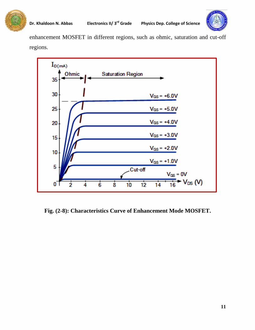
Dr. Khaldoon N. Abbas Electronics II/ 3rd Grade Physics Dep. College of Science
11
enhancement MOSFET in different regions, such as ohmic, saturation and cut-off
regions.
Fig. (2-8): Characteristics Curve of Enhancement Mode MOSFET.
Related Documents