Chapter 2 CMOS FABRICATION TECHNOLOGY AND DESIGN RULES Notice: This chapter is a largely based on Chapter 2 (Fabrication of MOSFETs) of the book CMOS Digital Integrated Circuit Design - Analysis and Design by S.M. Kang and Y. Leblebici. Introduction Fabrication Process Flow - Basic Steps The CMOS n-Well Process Advanced CMOS Fabrication Technologies Layout Design Rules 2.1 Introduction In this chapter, the fundamentals of MOS chip fabrication will be discussed and the major steps of the process flow will be examined. It is not the aim of this chapter to present a detailed discussion of silicon fabrication technology, which deserves separate treatment in a dedicated course. Rather, the emphasis will be on the general outline of the process flow and on the interaction of various processing steps, which ultimately determine the device and the circuit performance characteristics. The following chapters show that there are very strong links between the fabrication process, the circuit design process and the performance of the resulting chip. Hence, circuit designers must have a working knowledge of chip fabrication to create effective designs and in order to optimize the circuits with respect to various manufacturing parameters. Also, the circuit designer must have a clear understanding of the

Chapter 2 Cmos Fabrication Technology and Design Rules
Nov 18, 2014
Welcome message from author
This document is posted to help you gain knowledge. Please leave a comment to let me know what you think about it! Share it to your friends and learn new things together.
Transcript

Chapter 2 CMOS FABRICATION TECHNOLOGY AND DESIGN RULES
Notice: This chapter is a largely based on Chapter 2 (Fabrication of MOSFETs) of the book CMOS Digital Integrated Circuit Design - Analysis and Design by S.M. Kang and Y. Leblebici.
Introduction Fabrication Process Flow - Basic Steps The CMOS n-Well Process Advanced CMOS Fabrication Technologies Layout Design Rules
2.1 Introduction
In this chapter, the fundamentals of MOS chip fabrication will be discussed and the major steps of the process flow will be examined. It is not the aim of this chapter to present a detailed discussion of silicon fabrication technology, which deserves separate treatment in a dedicated course. Rather, the emphasis will be on the general outline of the process flow and on the interaction of various processing steps, which ultimately determine the device and the circuit performance characteristics. The following chapters show that there are very strong links between the fabrication process, the circuit design process and the performance of the resulting chip. Hence, circuit designers must have a working knowledge of chip fabrication to create effective designs and in order to optimize the circuits with respect to various manufacturing parameters. Also, the circuit designer must have a clear understanding of the roles of various masks used in the fabrication process, and how the masks are used to define various features of the devices on-chip.
The following discussion will concentrate on the well-established CMOS fabrication technology, which requires that both n-channel (nMOS) and p-channel (pMOS) transistors be built on the same chip substrate. To accommodate both nMOS and pMOS devices, special regions must be created in which the semiconductor type is opposite to the substrate type. These regions are called wells or tubs. A p-well is created in an n-type substrate or, alternatively, an n- well is created in a p-type substrate. In the simple n-well CMOS fabrication technology presented, the nMOS transistor is created in the p-type substrate, and the pMOS transistor is created in the n-well, which is built-in into the p-

type substrate. In the twin-tub CMOS technology, additional tubs of the same type as the substrate can also be created for device optimization.
The simplified process sequence for the fabrication of CMOS integrated circuits on a p- type silicon substrate is shown in Fig. 2.1. The process starts with the creation of the n-well regions for pMOS transistors, by impurity implantation into the substrate. Then, a thick oxide is grown in the regions surrounding the nMOS and pMOS active regions. The thin gate oxide is subsequently grown on the surface through thermal oxidation. These steps are followed by the creation of n+ and p+ regions (source, drain and channel-stop implants) and by final metallization (creation of metal interconnects).
[Click to enlarge image]
Figure-2.1: Simplified process sequence for fabrication of the n-well CMOS integrated circuit with a single polysilicon layer, showing only major fabrication steps.
The process flow sequence pictured in Fig. 2.1 may at first seem to be too abstract, since detailed fabrication steps are not shown. To obtain a better understanding of the issues involved in the semiconductor fabrication process, we first have to consider some of the basic steps in more detail.
2.2 Fabrication Process Flow - Basic Steps
Note that each processing step requires that certain areas are defined on chip by appropriate masks. Consequently, the integrated circuit may be viewed as a set of patterned layers of doped silicon, polysilicon, metal and insulating silicon dioxide. In general, a layer must be patterned before the next layer of material is applied on chip. The

process used to transfer a pattern to a layer on the chip is called lithography. Since each layer has its own distinct patterning requirements, the lithographic sequence must be repeated for every layer, using a different mask.
To illustrate the fabrication steps involved in patterning silicon dioxide through optical lithography, let us first examine the process flow shown in Fig. 2.2. The sequence starts with the thermal oxidation of the silicon surface, by which an oxide layer of about 1 micrometer thickness, for example, is created on the substrate (Fig. 2.2(b)). The entire oxide surface is then covered with a layer of photoresist, which is essentially a light-sensitive, acid-resistant organic polymer, initially insoluble in the developing solution (Fig. 2.2(c)). If the photoresist material is exposed to ultraviolet (UV) light, the exposed areas become soluble so that the they are no longer resistant to etching solvents. To selectively expose the photoresist, we have to cover some of the areas on the surface with a mask during exposure. Thus, when the structure with the mask on top is exposed to UV light, areas which are covered by the opaque features on the mask are shielded. In the areas where the UV light can pass through, on the other hand, the photoresist is exposed and becomes soluble (Fig. 2.2(d)).
[Click to enlarge image]

[Click to enlarge image]
Figure-2.2: Process steps required for patterning of silicon dioxide.
The type of photoresist which is initially insoluble and becomes soluble after exposure to UV light is called positive photoresist. The process sequence shown in Fig. 2.2 uses positive photoresist. There is another type of photoresist which is initially soluble and becomes insoluble (hardened) after exposure to UV light, called negative photoresist. If negative photoresist is used in the photolithography process, the areas which are not shielded from the UV light by the opaque mask features become insoluble, whereas the shielded areas can subsequently be etched away by a developing solution. Negative photoresists are more sensitive to light, but their photolithographic resolution is not as high as that of the positive photoresists. Therefore, negative photoresists are used less commonly in the manufacturing of high-density integrated circuits.
Following the UV exposure step, the unexposed portions of the photoresist can be removed by a solvent. Now, the silicon dioxide regions which are not covered by hardened photoresist can be etched away either by using a chemical solvent (HF acid) or by using a dry etch (plasma etch) process (Fig. 2.2(e)). Note that at the end of this step, we obtain an oxide window that reaches down to the silicon surface (Fig. 2.2(f)). The remaining photoresist can now be stripped from the silicon dioxide surface by using another solvent, leaving the patterned silicon dioxide feature on the surface as shown in Fig. 2.2(g).
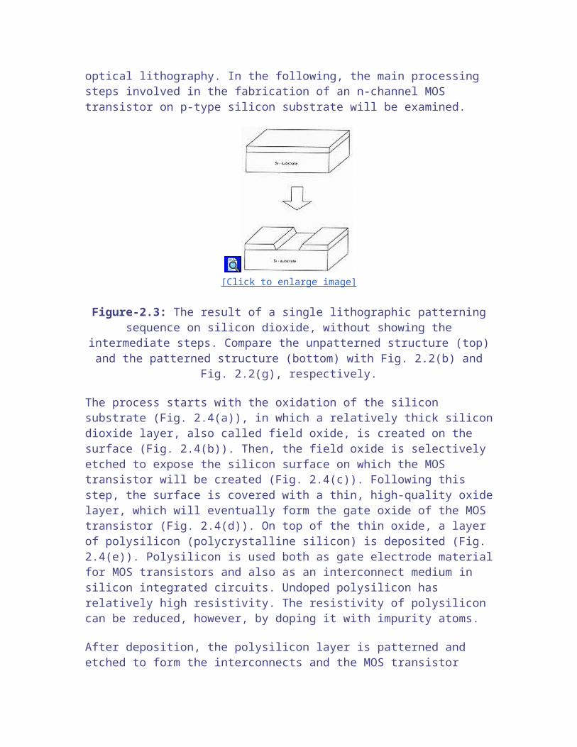
The sequence of process steps illustrated in detail in Fig. 2.2 actually accomplishes a single pattern transfer onto the silicon dioxide surface, as shown in Fig. 2.3. The fabrication of semiconductor devices requires several such pattern transfers to be performed on silicon dioxide, polysilicon, and metal. The basic patterning process used in

all fabrication steps, however, is quite similar to the one shown in Fig. 2.2. Also note that for accurate generation of high-density patterns required in sub-micron devices, electron beam (E-beam) lithography is used instead of optical lithography. In the following, the main processing steps involved in the fabrication of an n-channel MOS transistor on p-type silicon substrate will be examined.
[Click to enlarge image]
Figure-2.3: The result of a single lithographic patterning sequence on silicon dioxide, without showing the intermediate steps. Compare the unpatterned structure (top) and the
patterned structure (bottom) with Fig. 2.2(b) and Fig. 2.2(g), respectively.
The process starts with the oxidation of the silicon substrate (Fig. 2.4(a)), in which a relatively thick silicon dioxide layer, also called field oxide, is created on the surface (Fig. 2.4(b)). Then, the field oxide is selectively etched to expose the silicon surface on which the MOS transistor will be created (Fig. 2.4(c)). Following this step, the surface is covered with a thin, high-quality oxide layer, which will eventually form the gate oxide of the MOS transistor (Fig. 2.4(d)). On top of the thin oxide, a layer of polysilicon (polycrystalline silicon) is deposited (Fig. 2.4(e)). Polysilicon is used both as gate electrode material for MOS transistors and also as an interconnect medium in silicon integrated circuits. Undoped polysilicon has relatively high resistivity. The resistivity of polysilicon can be reduced, however, by doping it with impurity atoms.
After deposition, the polysilicon layer is patterned and etched to form the interconnects and the MOS transistor gates (Fig. 2.4(f)). The thin gate oxide not covered by polysilicon is also etched away, which exposes the bare silicon surface on which the source and drain junctions are to be formed (Fig. 2.4(g)). The entire silicon surface is then doped with a high concentration of impurities, either through diffusion or ion implantation (in this case with donor atoms to produce n-type doping). Figure 2.4(h) shows that the doping penetrates the exposed areas on the silicon surface, ultimately creating two n-type regions (source and drain junctions) in the p-type substrate. The impurity doping also penetrates the polysilicon on the surface, reducing its resistivity. Note that the polysilicon gate, which is patterned before doping actually defines the precise location of the channel region and, hence, the location of the source and the drain regions. Since this procedure

allows very precise positioning of the two regions relative to the gate, it is also called the self-aligned process.
[Click to enlarge image]
[Click to enlarge image]
[Click to enlarge image]
Figure-2.4: Process flow for the fabrication of an n-type MOSFET on p-type silicon.
Once the source and drain regions are completed, the entire surface is again covered with an insulating layer of silicon dioxide (Fig. 2.4(i)). The insulating oxide layer is then patterned in order to provide contact windows for the drain and source junctions (Fig.

2.4(j)). The surface is covered with evaporated aluminum which will form the interconnects (Fig. 2.4(k)). Finally, the metal layer is patterned and etched, completing the interconnection of the MOS transistors on the surface (Fig. 2.4(l)). Usually, a second (and third) layer of metallic interconnect can also be added on top of this structure by creating another insulating oxide layer, cutting contact (via) holes, depositing, and patterning the metal.
2.3 The CMOS n-Well Process
Having examined the basic process steps for pattern transfer through lithography, and having gone through the fabrication procedure of a single n-type MOS transistor, we can now return to the generalized fabrication sequence of n-well CMOS integrated circuits, as shown in Fig. 2.1. In the following figures, some of the important process steps involved in the fabrication of a CMOS inverter will be shown by a top view of the lithographic masks and a cross-sectional view of the relevant areas.
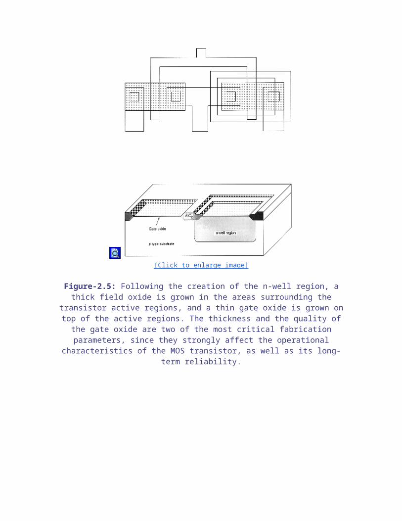
The n-well CMOS process starts with a moderately doped (with impurity concentration typically less than 1015 cm-3) p-type silicon substrate. Then, an initial oxide layer is grown on the entire surface. The first lithographic mask defines the n-well region. Donor atoms, usually phosphorus, are implanted through this window in the oxide. Once the n-well is created, the active areas of the nMOS and pMOS transistors can be defined. Figures 2.5 through 2.10 illustrate the significant milestones that occur during the fabrication process of a CMOS inverter.

[Click to enlarge image]
Figure-2.5: Following the creation of the n-well region, a thick field oxide is grown in the areas surrounding the transistor active regions, and a thin gate oxide is grown on top of the active regions. The thickness and the quality of the gate oxide are two of the most
critical fabrication parameters, since they strongly affect the operational characteristics of the MOS transistor, as well as its long-term reliability.

[Click to enlarge image]
Figure-2.6: The polysilicon layer is deposited using chemical vapor deposition (CVD) and patterned by dry (plasma) etching. The created polysilicon lines will function as the gate electrodes of the nMOS and the pMOS transistors and their interconnects. Also, the
polysilicon gates act as self-aligned masks for the source and drain implantations that follow this step.

[Click to enlarge image]
Figure-2.7: Using a set of two masks, the n+ and p+ regions are implanted into the substrate and into the n- well, respectively. Also, the ohmic contacts to the substrate and
to the n-well are implanted in this process step.
[Click to enlarge image]
Figure-2.8: An insulating silicon dioxide layer is deposited over the entire wafer using CVD. Then, the contacts are defined and etched away to expose the silicon or polysilicon
contact windows. These contact windows are necessary to complete the circuit interconnections using the metal layer, which is patterned in the next step.

[Click to enlarge image]
Figure-2.9: Metal (aluminum) is deposited over the entire chip surface using metal evaporation, and the metal lines are patterned through etching. Since the wafer surface is
non-planar, the quality and the integrity of the metal lines created in this step are very critical and are ultimately essential for circuit reliability.

[Click to enlarge image]
Figure-2.10: The composite layout and the resulting cross-sectional view of the chip, showing one nMOS and one pMOS transistor (built-in n-well), the polysilicon and metal interconnections. The final step is to deposit the passivation layer (for protection) over
the chip, except for wire-bonding pad areas.
The patterning process by the use of a succession of masks and process steps is conceptually summarized in Fig. 2.11. It is seen that a series of masking steps must be sequentially performed for the desired patterns to be created on the wafer surface. An example of the end result of this sequence is shown as a cross-section on the right.

[Click to enlarge image]
Figure-2.11: Conceptual illustration of the mask sequence applied to create desired structures.
2.4 Advanced CMOS Fabrication Technologies
In this section, two examples will be given for advanced CMOS processes which offer additional benefits in terms of device performance and integration density. These processes, namely, the twin-tub CMOS process and the silicon-on-insulator (SOI) process, are becoming especially more popular for sub-micron geometries where device performance and density must be pushed beyond the limits of the conventional n-well CMOS process.
Twin-Tub (Twin-Well) CMOS Process
This technology provides the basis for separate optimization of the nMOS and pMOS transistors, thus making it possible for threshold voltage, body effect and the channel transconductance of both types of transistors to be tuned independently. Generally, the starting material is a n+ or p+ substrate, with a lightly doped epitaxial layer on top. This epitaxial layer provides the actual substrate on which the n-well and the p-well are formed. Since two independent doping steps are performed for the creation of the well regions, the dopant concentrations can be carefully optimized to produce the desired device characteristics.
In the conventional n-well CMOS process, the doping density of the well region is typically about one order of magnitude higher than the substrate, which, among other

effects, results in unbalanced drain parasitics. The twin-tub process (Fig. 2.12) also avoids this problem.
[Click to enlarge image]
Figure-2.12: Cross-section of nMOS and pMOS transistors in twin-tub CMOS process.
Silicon-on-Insulator (SOI) CMOS Process
Rather than using silicon as the substrate material, technologists have sought to use an insulating substrate to improve process characteristics such as speed and latch-up susceptibility. The SOI CMOS technology allows the creation of independent, completely isolated nMOS and pMOS transistors virtually side-by-side on an insulating substrate (for example: sapphire). The main advantages of this technology are the higher integration density (because of the absence of well regions), complete avoidance of the latch-up problem, and lower parasitic capacitances compared to the conventional n-well or twin-tub CMOS processes. A cross-section of nMOS and pMOS devices in created using SOI process is shown in Fig. 2.13.
The SOI CMOS process is considerably more costly than the standard n-well CMOS process. Yet the improvements of device performance and the absence of latch-up problems can justify its use, especially for deep-sub-micron devices.
[Click to enlarge image]
Figure-2.13: Cross-section of nMOS and pMOS transistors in SOI CMOS process.

2.5 Layout Design Rules
The physical mask layout of any circuit to be manufactured using a particular process must conform to a set of geometric constraints or rules, which are generally called layout design rules. These rules usually specify the minimum allowable line widths for physical objects on-chip such as metal and polysilicon interconnects or diffusion areas, minimum feature dimensions, and minimum allowable separations between two such features. If a metal line width is made too small, for example, it is possible for the line to break during the fabrication process or afterwards, resulting in an open circuit. If two lines are placed too close to each other in the layout, they may form an unwanted short circuit by merging during or after the fabrication process. The main objective of design rules is to achieve a high overall yield and reliability while using the smallest possible silicon area, for any circuit to be manufactured with a particular process.
Note that there is usually a trade-off between higher yield which is obtained through conservative geometries, and better area efficiency, which is obtained through aggressive, high- density placement of various features on the chip. The layout design rules which are specified for a particular fabrication process normally represent a reasonable optimum point in terms of yield and density. It must be emphasized, however, that the design rules do not represent strict boundaries which separate "correct" designs from "incorrect" ones. A layout which violates some of the specified design rules may still result in an operational circuit with reasonable yield, whereas another layout observing all specified design rules may result in a circuit which is not functional and/or has very low yield. To summarize, we can say, in general, that observing the layout design rules significantly increases the probability of fabricating a successful product with high yield.
The design rules are usually described in two ways :
Micron rules, in which the layout constraints such as minimum feature sizes and minimum allowable feature separations, are stated in terms of absolute dimensions in micrometers, or,
Lambda rules, which specify the layout constraints in terms of a single parameter (?) and, thus, allow linear, proportional scaling of all geometrical constraints.
Lambda-based layout design rules were originally devised to simplify the industry- standard micron-based design rules and to allow scaling capability for various processes. It must be emphasized, however, that most of the submicron CMOS process design rules do not lend themselves to straightforward linear scaling. The use of lambda-based design rules must therefore be handled with caution in sub-micron geometries. In the following, we present a sample set of the lambda-based layout design rules devised for the MOSIS CMOS process and illustrate the implications of these rules on a section a simple layout which includes two transistors (Fig. 2.14).
MOSIS Layout Design Rules (sample set)

Rule number Description L-Rule
R1 Minimum active area width 3 LR2 Minimum active area spacing 3 L
R3 Minimum poly width 2 LR4 Minimum poly spacing 2 LR5 Minimum gate extension of poly over active 2 LR6 Minimum poly-active edge spacing 1 L
(poly outside active area)R7 Minimum poly-active edge spacing 3 L
(poly inside active area)
R8 Minimum metal width 3 LR9 Minimum metal spacing 3 L
R10 Poly contact size 2 LR11 Minimum poly contact spacing 2 LR12 Minimum poly contact to poly edge spacing 1 LR13 Minimum poly contact to metal edge spacing 1 LR14 Minimum poly contact to active edge spacing 3 L
R15 Active contact size 2 LR16 Minimum active contact spacing 2 L
(on the same active region)R17 Minimum active contact to active edge spacing 1 LR18 Minimum active contact to metal edge spacing 1 LR19 Minimum active contact to poly edge spacing 3 LR20 Minimum active contact spacing 6 L
(on different active regions)

[Click to enlarge image]
Figure-2.14: Illustration of some of the typical MOSIS layout design rules listed above.
References
1. W. Maly, Atlas of IC Technologies, Menlo Park, CA: Benjamin/Cummings, 1987.
2. A. S. Grove, Physics and Technology of Semiconductor Devices, New York, NY: John Wiley & Sons, Inc., 1967.
3. G. E. Anner, Planar Processing Primer, New York, NY: Van Nostrand Rheinhold, 1990.
4. T. E. Dillinger, VLSI Engineering, Englewood Cliffs, NJ: Prentice-Hall, Inc., 1988.
5. S.M. Sze, VLSI Technology, New York, NY: McGraw-Hill, 1983.

This chapter edited by Y. Leblebici
Chapter 3FULL-CUSTOM MASK LAYOUT
DESIGN
Introduction CMOS Layout Design Rules CMOS Inverter Layout Design Layout of CMOS NAND and NOR Gates Complex CMOS Logic Gates
3.1 Introduction
In this chapter, the basic mask layout design guidelines for CMOS logic gates will be presented. The design of physical layout is very tightly linked to overall circuit performance (area, speed, power dissipation) since the physical structure directly determines the transconductances of the transistors, the parasitic capacitances and resistances, and obviously, the silicon area which is used for a certain function. On the other hand, the detailed mask layout of logic gates requires a very intensive and time-consuming design effort, which is justifiable only in special circumstances where the area and/or the performance of the circuit must be optimized under very tight constraints. Therefore, automated layout generation (e.g., standard cells + computer-aided placement and routing) is typically preferred for the design of most digital VLSI circuits. In order to judge the physical constraints and limitations, however, the VLSI designer must also have a good understanding of the physical mask layout process.
Mask layout drawings must strictly conform to a set of layout design rules as described in Chapter 2, therefore, we will start this chapter with the review of a complete design rule set. The design of a simple CMOS inverter will be presented step-by-step, in order to

show the influence of various design rules on the mask structure and on the dimensions. Also, we will introduce the concept of stick diagrams, which can be used very effectively to simplify the overall topology of layout in the early design phases. With the help of stick diagrams, the designer can have a good understanding of the topological constraints, and quickly test several possibilities for the optimum layout without actually drawing a complete mask diagram.
The physical (mask layout) design of CMOS logic gates is an iterative process which starts with the circuit topology (to realize the desired logic function) and the initial sizing of the transistors (to realize the desired performance specifications). At this point, the designer can only estimate the total parasitic load at the output node, based on the fan-out, the number of devices, and the expected length of the interconnection lines. If the logic gate contains more than 4-6 transistors, the topological graph representation and the Euler-path method allow the designer to determine the optimum ordering of the transistors. A simple stick diagram layout can now be drawn, showing the locations of the transistors, the local interconnections between the transistors and the locations of the contacts.
After a topologically feasible layout is found, the mask layers are drawn (using a layout editor tool) according to the layout design rules. This procedure may require several small iterations in order to accommodate all design rules, but the basic topology should not change very significantly. Following the final DRC (Design Rule Check), a circuit extraction procedure is performed on the finished layout to determine the actual transistor sizes, and more importantly, the parasitic capacitances at each node. The result of the extraction step is usually a detailed

[Click to enlarge image]
Figure-3.1: The typical design flow for the production of a mask layout.
SPICE input file, which is automatically generated by the extraction tool. Now, the actual performance of the circuit can be determined by performing a SPICE simulation, using the extracted net-list. If the simulated circuit performance (e.g., transient response times or power dissipation) do not match the desired specifications, the layout must be modified and the whole process must be repeated. The layout modifications are usually concentrated on the (W/L) ratios of the transistors (transistor re-sizing), since the width-to-length ratios of the transistors determine the device transconductance and the parasitic source/drain capacitances. The designer may also decide to change parts or all of the circuit topology in order to reduce the parasitics. The flow diagram of this iterative process is shown in Fig. 3.1.

3.2 CMOS Layout Design Rules
As already discussed in Chapter 2, each mask layout design must conform to a set of layout design rules, which dictate the geometrical constraints imposed upon the mask layers by the technology and by the fabrication process. The layout designer must follow these rules in order to guarantee a certain yield for the finished product, i.e., a certain ratio of acceptable chips out of a fabrication batch. A design which violates some of the layout design rules may still result in a functional chip, but the yield is expected to be lower because of random process variations.
The design rules below are given in terms of scaleable lambda-rules. Note that while the concept of scaleable design rules is very convenient for defining a technology-independent mask layout and for memorizing the basic constraints, most of the rules do not scale linearly, especially for sub-micron technologies. This fact is illustrated in the right column, where a representative rule set is given in real micron dimensions. A simple comparison with the lambda- based rules shows that there are significant differences. Therefore, lambda-based design rules are simply not useful for sub-micron CMOS technologies.

[Click to enlarge image]

[Click to enlarge image]
Figure-3.2: Illustration of CMOS layout design rules.
3.3 CMOS Inverter Layout Design
In the following, the mask layout design of a CMOS inverter will be examined step-by-step. The circuit consists of one nMOS and one pMOS transistor, therefore, one would assume that the layout topology is relatively simple. Yet, we will see that there exist quite a number of different design possibilities even for this very simple circuit.
First, we need to create the individual transistors according to the design rules. Assume that we attempt to design the inverter with minimum-size transistors. The width of the active area is then determined by the minimum diffusion contact size (which is necessary for source and drain connections) and the minimum separation from diffusion contact to both active area edges. The width of the polysilicon line over the active area (which is the gate of the transistor) is typically taken as the minimum poly width (Fig. 3.3). Then, the overall length of the active area is simply determined by the following sum: (minimum poly width) + 2 x (minimum poly-to- contact spacing) + 2 x (minimum spacing from contact to active area edge). The pMOS transistor must be placed in an n-well region, and the minimum size of the n- well is dictated by the pMOS active area and the minimum n-well overlap over n+. The distance between the nMOS and the pMOS transistor is determined by the minimum separation between the n+ active area and the n-well (Fig. 3.4). The polysilicon gates of the nMOS and the pMOS transistors are usually aligned.

The final step in the mask layout is the local interconnections in metal, for the output node and for the VDD and GND contacts (Fig. 3.5). Notice that in order to be biased properly, the n-well region must also have a VDD contact.
[Click to enlarge image]
Figure-3.3: Design rule constraints which determine the dimensions of a minimum-size transistor.
[Click to enlarge image]
Figure-3.4: Placement of one nMOS and one pMOS transistor.

[Click to enlarge image]
Figure-3.5: Complete mask layout of the CMOS inverter.
The inital phase of layout design can be simplified significantly by the use of stick diagrams - or so-called symbolic layouts. Here, the detailed layout design rules are simply neglected and the main features (active areas, polysilicon lines, metal lines) are represented by constant width rectangles or simple sticks. The purpose of the stick diagram is to provide the designer a good understanding of the topological constraints, and to quickly test several possibilities for the optimum layout without actually drawing a complete mask diagram. In the following, we will examine a series of stick diagrams which show different layout options for the CMOS inverter circuit.
The first two stick diagram layouts shown in Fig. 3.6 are the two most basic inverter configurations, with different alignments of the transistors. In some cases, other signals must be routed over the inverter. For instance, if one or two metal lines have to be passed through the middle of the cell from left to right, horizontal metal straps can be used to access the drain terminals of the transistors, which in turn connect to a vertical Metal-2 line. Metal-1 can now be used to route the signals passing through the inverter. Alternatively, the diffusion areas of both transistors may be used for extending the power and ground connections. This makes the inverter transistors transparent to horizontal metal lines which may pass over.
The addition of a second metal layer allows more interconnect freedom. The second- level metal can be used for power and ground supply lines, or alternatively, it may be used to vertically strap the input and the output signals. The final layout example in Fig. 3.6 shows one possibility of using a third metal layer, which is utilized for routing three signals on top.

[Click to enlarge image]
Figure-3.6: Stick diagrams showing various CMOS inverter layout options.
3.4 Layout of CMOS NAND and NOR Gates
The mask layout designs of CMOS NAND and NOR gates follow the general principles examined earlier for the CMOS inverter layout. Figure 3.7 shows the sample layouts of a two- input NOR gate and a two-input NAND gate, using single-layer polysilicon and single-layer metal. Here, the p-type diffusion area for the pMOS transistors and the n-type diffusion area for the nMOS transistors are aligned in parallel to allow simple

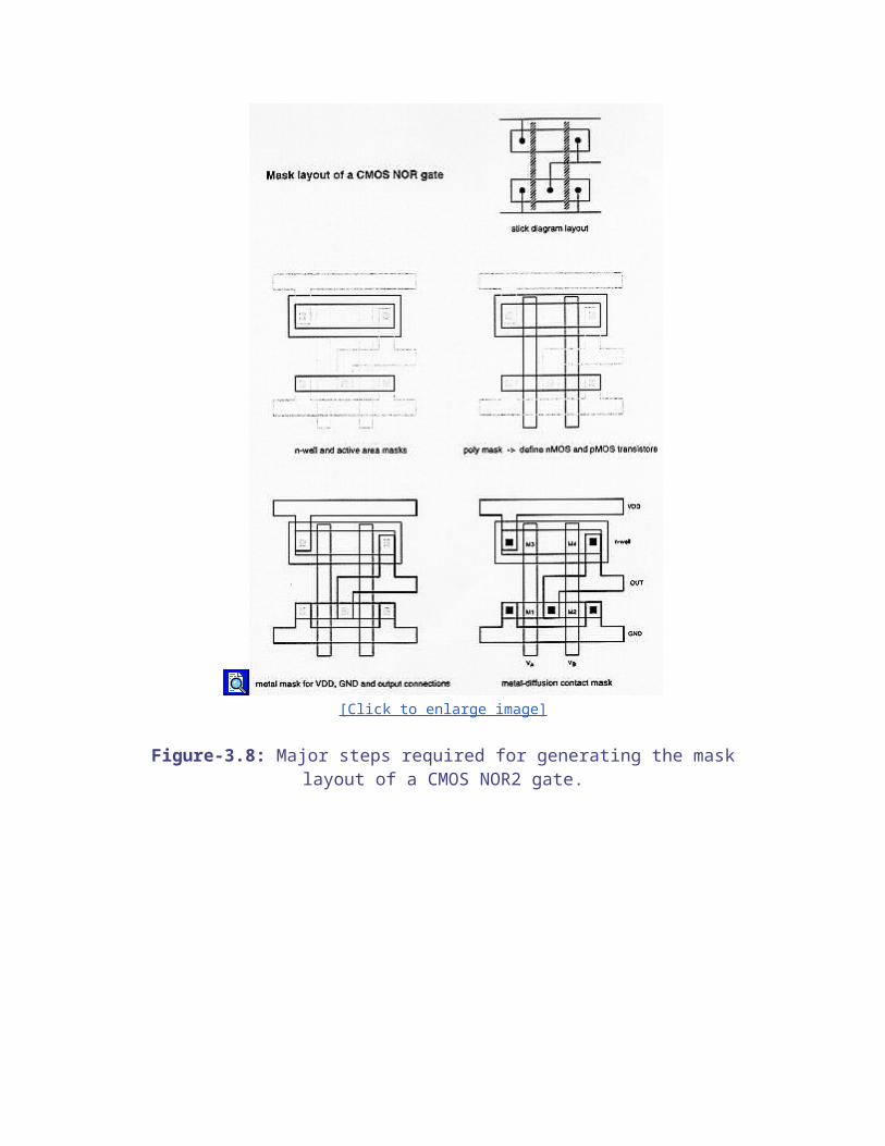
routing of the gate signals with two parallel polysilicon lines running vertically. Also notice that the two mask layouts show a very strong symmetry, due to the fact that the NAND and the NOR gate are have a symmetrical circuit topology. Finally, Figs 3.8 and 3.9 show the major steps of the mask layout design for both gates, starting from the stick diagram and progressively defining the mask layers.
[Click to enlarge image]
Figure-3.7: Sample layouts of a CMOS NOR2 gate and a CMOS NAND2 gate.

[Click to enlarge image]
Figure-3.8: Major steps required for generating the mask layout of a CMOS NOR2 gate.

[Click to enlarge image]
Figure-3.9: Major steps required for generating the mask layout of a CMOS NAND2 gate.
3.5 Complex CMOS Logic Gates
The realization of complex Boolean functions (which may include several input variables and several product terms) typically requires a series-parallel network of nMOS transistors which constitute the so-called pull-down net, and a corresponding dual network of pMOS transistors which constitute the pull-up net. Figure 3.10 shows the circuit diagram and the corresponding network graphs of a complex CMOS logic gate.

Once the network topology of the nMOS pull- down network is known, the pull-up network of pMOS transistors can easily be constructed by using the dual-graph concept.
[Click to enlarge image]
Figure-3.10: A complex CMOS logic gate realizing a Boolean function with 5 input variables.
Now, we will investigate the problem of constructing a minimum-area layout for the complex CMOS logic gate. Figure 3.11 shows the stick-diagram layout of a “first-attempt”, using an arbitrary ordering of the polysilicon gate columns. Note that in this case, the separation between the polysilicon columns must be sufficiently wide to allow for two metal-diffusion contacts on both sides and one diffusion-diffusion separation. This certainly consumes a considerable amount of extra silicon area.
If we can minimize the number of active-area breaks both for the nMOS and for the pMOS transistors, the separation between the polysilicon gate columns can be made smaller. This, in turn, will reduce the overall horizontal dimension and the overall circuit layout area. The number of active-area breaks can be minimized by changing the ordering of the polysilicon columns, i.e., by changing the ordering of the transistors.

[Click to enlarge image]
Figure-3.11: Stick diagram layout of the complex CMOS logic gate, with an arbitrary ordering of the polysilicon gate columns.
A simple method for finding the optimum gate ordering is the Euler-path method: Simply find a Euler path in the pull-down network graph and a Euler path in the pull-up network graph with the identical ordering of input labels, i.e., find a common Euler path for both graphs. The Euler path is defined as an uninterrupted path that traverses each edge (branch) of the graph exactly once. Figure 3.12 shows the construction of a common Euler path for both graphs in our example.
[Click to enlarge image]
Figure-3.12: Finding a common Euler path in both graphs for the pull-down and pull-up net provides a gate ordering that minimizes the number of active-area breaks. In both
cases, the Euler path starts at (x) and ends at (y).
It is seen that there is a common sequence (E-D-A-B-C) in both graphs. The polysilicon gate columns can be arranged according to this sequence, which results in uninterrupted active areas for nMOS as well as for pMOS transistors. The stick diagram of the new layout is shown in Fig. 3.13. In this case, the separation between two neighboring poly columns must allow only for one metal-diffusion contact. The advantages of this new layout are more compact (smaller) layout area, simple routing of signals, and correspondingly, smaller parasitic capacitance.

[Click to enlarge image]
Figure-3.13: Optimized stick diagram layout of the complex CMOS logic gate.
It may not always be possible to construct a complete Euler path both in the pull-down and in the pull-up network. In that case, the best strategy is to find sub-Euler-paths in both graphs, which should be as long as possible. This approach attempts to maximize the number of transistors which can be placed in a single, uninterrupted active area.
Finally, Fig. 3.14 shows the circuit diagram of a CMOS one-bit full adder. The circuit has three inputs, and two outputs, sum and carry_out. The corresponding mask layout of this circuit is given in Fig. 3.15. All input and output signals have been arranged in vertical polysilicon columns. Notice that both the sum-circuit and the carry-circuit have been realized using one uninterrupted active area each.
[Click to enlarge image]
Figure-3.14: Circuit diagram of the CMOS one-bit full adder.
[Click to enlarge image]
Figure-3.15: Mask layout of the CMOS full adder circuit..
This chapter edited by Y. Leblebici
production of
Chapter 8TESTABILITY OF INTEGRATED
SYSTEMS
Design Constraints Testing

The Rule of Ten Terminology Failures in CMOS Combinational Logic Testing Practical Ad-Hoc DFT Guidelines Scan Design Techniques
8.1 Design Constraints
The following paragraphs reminds the designer of some basic rules to consider before starting. Each of these constraints has at least one tool helping in the development of the design in respect to a set of rules :
8.1.1 Design Rule Checking
Every technology has its design rules. It consists in interpreting the possible geometrical implementation of the chips to be manufactured. These rules are given by the technology department in every foundry of IC. Rules are often described in a document with boxes representing the layers available in the technology on which are indicated the sizes, distances and geometrical constraints allowed in this technology.
[Click to enlarge image]
Figure-8.1:
Designer needs to execute a program called DRC to check if his design don't violate the rules defined by the founder. This step of verification called DRC is as important as the simulation of the functionality of your design. A sole simulation can't take in consideration if the rules are respected in which case the manufacturing of the chip could lead to shorts or cuts in the silicon physical implementation. Some other verification tools should also be used, such as ERC and LVS described above.
8.1.2 Layout Versus Schematic

As a complement to the DRC, LVS is another tool to be used especially if the design started with a Schematic Entry tool. The aim of LVS is to check if the design at the layout level corresponds or is still coherent to the schematic. Usually, designers start with a schematic and then simulate it, if it is OK then they go to layout. But in some cases like full-custom or some semi-custom designs the layout implementation of the chip differs from the schematic because of some simulation results or because of a design error that simulation can't detect easily : simulation could never be exhaustive. LVS checks that the designer did the same representation at the schematic and layout levels, if not LVS tools indicate the occurrence. Of course a simulation of the layout using the same stimuli used for the schematic is more secure for the final design.
8.1.3 Latch-Up and Electro-Static Discharge
Latch-up caused to CMOS the early problems that delayed its introduction in the electronic industry. It also called "Thyristor effect" and could cause the destruction of the chip or a part of it. There are no real solution to this phenomena but a set of design techniques exist to avoid instead of solving Latch-up occurence. The origin of Latch-up is the distribution of the NMOS and PMOS N and P basic structures inside the silicon. In some cases, not only PN junction are formed but also a structure like PNPN or NPNP parasitic thyristors. these parasitic elements could feature like a real thyristor and develop a high current destroying the area around it including the PMOS and NMOS transistors.
The most used technique in avoiding the formation of such a structure is to add "butting contact" polarising the Nwell (or Pwell) to Vdd (or to Ground). This technique cannot eliminate the Latch-up process but reduces its effect.
Another electrical constraint to CMOS is called ESD or Electro-Static Discharge. Handling CMOS chip properly could be a solution to avoid gates destruction caused by electro- static charges that people could have at the surface of their hands. This is the reason why it is important to have a conducting bracelet linked to ground when handling CMOS ICs. But even ground linked bracelet is not enough to protect CMOS chips from destruction due to ESD. Two diodes at each pad inside the chip link every I/O to Vdd and Gnd. These two big diodes protect the chip core (CMOS transistor gates) from ESD by limiting over-voltage.
[Click to enlarge image]

Figure-8.2:
8.1.4 Electrical Rule Checking
Based on the previous paragraph, ERC is a guarantee that the designer has considered all the minimum necessary implementations for ERC free design. This tool verifies that the designer did used a sufficient number of well polarisations, applied the appropriate ESD pads or used VDD and VSS at the right places.
8.2 Testing
Design of logic integrated circuits in CMOS technology is becoming more and more complex since VLSI is the interest of many electronic IC users and manufacturers. A common problem to be solved by both users and manufacturers is the testing of these ICs.
[Click to enlarge image]
Figure-8.3:
Testing can be expressed by checking if the outputs of a functional system (functional block, Integrated Circuit, Printed Circuit Board or a complete system) correspond to the inputs applied to it. If the test of this functional system is positive, then the system is good for use. If the outputs are different than expected, then the system has a problem: so either the system is rejected (Go/No Go test), or a diagnosis is applied to it, in order to point out and probably eliminate the problem's causes.
Testing is applied to detect faults after several operations : design, manufacturing, packaging and especially during the active life of a system, and thus since failures caused by wear-out can occur at any moment of its usage.

Design for Testability (DfT) is the ability of simplifying the test of any system. DfT could be synthesized by a set of techniques and design guidelines where the goals are :
minimizing costs of system production minimizing system test complexity : test generation and application improving quality avoiding problems of timing discordance or block nature incompatibility.
8.3 The Rule of Ten
In the production process cycle, a fault can occur at the chip level. If a test strategy is considered at the beginning of the design, then the fault could be detected rapidly, located and eliminated at a very low cost. When the faulty chip is soldered on a printed circuit board, the cost of fault remedy would be multiplied by ten. And this cost factors continues to apply until the system has been assembled and packaged and then sent to users.
[Click to enlarge image]
Figure-8.4:
8.4 Terminology
At the system level the most used words are the following:

Testability could be expressed by the ability for a Device Under Test (DUT), to be better observed and controlled easily from its external environment.
[Click to enlarge image]
Figure-8.5:
The Design for Testability is then reduced to a set of design rules or guidelines to be respected in order to facilitate the test.
The Reliability is expressed in terms of probability for a device to work without major problems for a given time. Reliability goes down when components number is increased.
The Security is the probability that user's life is not in danger while a problem occurs to a device. Security is enhanced if a certain type components are added for more protection.
The Quality is essential in some types of applications. A "zero defect" target is often required. The Quality could be enhanced by having a proper design methodology, and a good technology, avoiding problems and simplifying testing.
8.5 Failures in CMOS
When a MOS circuit has been fabricated and initially tested, some mechanisms can still cause it to fail. Failures are caused either by design bugs or by wearout (ageing or corrosion) mechanisms. The MOSFET transistor currently used has two main characteristics : threshold voltage and transconductance on which the performance of that circuit depends.

[Click to enlarge image]
Figure-8.6:
The design bugs or defects result generally in device length and width deviating from those specified for a process (design rules). This type of fault is difficult to detect since it occurs later during the active life of the circuit, and leads mostly to opens and breaks in conductors or shorts between conductors.
Failures are also caused by phenomena like "hot carrier injection", "oxide breakdown", "metallization failures" or "corrosion".
The consequences of hot carrier injection, for instance, is a threshold voltage shifting and transconductance degrading because the gate oxide is charged when hot carriers are injected (usually electron in NMOS). Cross-talk is also a cause of faults (generally transient), and needs to isolate properly the different parts of the device.
8.6 Combinational Logic Testing
It is more convenient to talk about "test generation for combinational logic testing" in this section, and about "test generation for sequential logic testing" in the next section. Thus the solution to the problem of testing a purely combinational logic block is a good set of patterns detecting "all" the possible faults.
The first idea to test an N input circuit would be to apply an N-bit counter to the inputs (controllability), then generate all the 2N combinations, and observe the outputs for checking (observability). This is called "exhaustive testing", and it is very efficient... but

only for few- input circuits. When the input number increase, this technique becomes very time consuming.
[Click to enlarge image]
Figure-8.7:
8.6.1 Sensitized Path Testing
Most of the time, in exhaustive testing, many patterns do not occur during the application of the circuit. So instead of spending a huge amount of time searching for faults everywhere, the possible faults are first enumerated and a set of appropriate vectors are then generated. This is called "single-path sensitization" and it is based on "fault oriented testing".
[Click to enlarge image]
Figure-8.8:
The basic idea is to select a path from the site of a fault, through a sequence of gates leading to an output of the combinational logic under test. The process is composed of three steps :

Manifestation : gate inputs, at the site of the fault, are specified as to generate the opposite value of the faulty value (0 for SA1, 1 for SA0).
Propagation : inputs of the other gates are determined so as to propagate the fault signal along the specified path to the primary output of the circuit. This is done by setting these inputs to "1" for AND/NAND gates and "0" for OR/NOR gates.
Consistency : or justification. This final step helps finding the primary input pattern that will realize all the necessary input values. This is done by tracing backward from the gate inputs to the primary inputs of the logic in order to receive the test patterns.
[Click to enlarge image]
Figure-8.9:
EXAMPLE1 - SA1 of line1 (L1) : the aim is to find the vector(s) able to detect this fault.
Manifestation : L1 = 0 , then input A = 0. In a fault-free situation, the output F changes with A if B,C and D are fixed : for B,C and D fixed, L1 is SA1 gives F = 0, for instance, even if A = 0 (F = 1 for fault-free).
Propagation : Through the AND-gate : L5 = L8 = 1, this condition is necessary for the propagation of the " L1 = 0 ". This leads to L10 = 0. Through the NOR-gate, and since L10 = 0, then L11 = 0, so the propagated manifestation can reach the primary output F. F is then read and compared with the fault-free value : F = 1.
Consistency : From the AND-gate : L5=1, and then L2=B=1. Also L8=1, and then L7=1. Until now we found the values of A and B. When C and D are found, then the test vectors are generated, in the same manner, and ready to be applied to detect L1= SA1. From the NOT-gate, L11=0, so L9=L7=1 (coherency with L8=L7). From the OR-gate L7=1, and since L6=L2=B=1, so B+C+D=L7=1, then C and D can have either 1 or 0.
These three steps have led to four possible vectors detecting L1=SA1.

[Click to enlarge image]
Figure-8.10:
EXAMPLE 2 - SA1 of line8 (L8) : The same combinational logic having one internal line SA1.
Manifestation : L8 = 0 Propagation : Through the AND-gate : L5 = L1 = 1, then L10 = 0 Through the
NOR-gate : we want to have L11 = 0, not to mask L10 = 0. Consistency : From the AND-gate L8 = 0 leads to L7 = 0. From the NOT-gate
L11 = 0 means L9 = L7 = 1, L7 could not be set to 1 and 0 at the same time. This incompatibility could not be resolved in this case, and the fault "L8 SA1" remains undetectable.
[Click to enlarge image]
Figure-8.11:
EXAMPLE 3 - SA1 of line2 (L2) : Always the same combinational logic, with the line L2 SA1.

Manifestation : L2 = 0, sets L5 = L6 = 0. Propagation : Through the AND-gate : L1 = 1 and then we need L10=0. Through
the OR-gate L3=L4=0, so we can have L7=L8=L9=0, but through the NOT-gate L11 = 1.
The propagated error "L2 SA1" across a reconvergent path is masked since the NOR-gate does not distinguish the origin of the propagation.
8.7 Practical Ad-Hoc DFT Guidelines
This section provides a set of practical Design for Testability guidelines classified into three types: those who are facilitating test generation, test application and those avoiding timing problems.
8.7.1 Improve Controllability and Observability
All "design for test" methods ensure that a design has enough observability and controllability to provide for a complete and efficient testing. When a node has difficult access from primary inputs or outputs (pads of the circuit), a very efficient method is to add internal pads acceding to this kind of node in order, for instance, to control block B2 and observe block B1 with a probe.
[Click to enlarge image]
Figure-8.12:
It is easy to observe block B1 by adding a pad just on its output, without breaking the link between the two blocks. The control of the block B2 means to set a 0 or a 1 to its input, and also to be transparent to the link B1-B2. The logic functions of this purpose are a NOR- gate, transparent to a zero, and a NAND-gate, transparent to a one. By this way the control of B2 is possible across these two gates.

Another implementation of this cell is based on pass-gates multiplexers performing the same function, but with less transistors than with the NAND and NOR gates (8 instead of 12).
The simple optimization of observation and control is not enough to guarantee a full testability of the blocks B1 and B2. This technique has to be completed with some other techniques of testing depending on the internal structures of blocks B1 and B2.
8.7.2 Use Multiplexers
This technique is an extension of the precedent, while multiplexers are used in case of limitation of primary inputs and outputs.
[Click to enlarge image]
Figure-8.13:
In this case the major penalties are extra devices and propagation delays due to multiplexers. Demultiplexers are also used to improve observability. Using multiplexers and demultiplexers allows internal access of blocks separately from each other, which is the basis of techniques based on partitioning or bypassing blocks to observe or control separately other blocks.
8.7.3 Partition Large Circuits
Partitioning large circuits into smaller sub-circuits reduces the test-generation effort. The test- generation effort for a general purpose circuit of n gates is assumed to be proportional to somewhere between n2 and n3. If the circuit is partitioned into two sub-circuits, then the amount of test generation effort is reduced correspondingly.

[Click to enlarge image]
Figure-8.14:
The example of the SN7480 full adder shows that an exhaustive testing requires 512 tests (29), while a full test after partitioning into four sub-circuits, for SA0 and SA1 faults, requires 24 tests. Logical partitioning of a circuit should be based on recognizable sub-functions and can be achieved physically by incorporating some facilities to isolate and control clock lines, reset lines and power supply lines. The multiplexers can be massively used to separate sub-circuits without changing the function of the global circuit.
8.7.4 Divide Long Counter Chains
Based on the same principle of partitioning, the counters are sequential elements that need a large number of vectors to be fully tested. The partitioning of a long counter corresponds to its division into sub-counters.
The full test of a 16-bit counter requires the application of 216 + 1 = 65537 clock pulses. If this counter is divided into two 8-bit counters, then each counter can be tested separately, and the total test time is reduced 128 times (27). This is also useful if there are subsequent requirements to set the counter to a particular count for tests associated with other parts of the circuit : pre-loading facilities.

[Click to enlarge image]
Figure-8.15:
8.7.5 Initialize Sequential Logic
One of the most important problems in sequential logic testing occurs at the time of power-on, where the first state is random if there were no initialization. In this case it is impossible to start a test sequence correctly, because of memory effects of the sequential elements.
[Click to enlarge image]
Figure-8.16:
The solution is to provide flip-flops or latches with a set or reset input, and then to use them so that the test sequence would start with a known state.
Ideally, all memory elements should be able to be set to a known state, but practically this could be very surface consuming, also it is not always necessary to initialize all the sequential logic. For example, a serial-in serial-out counter could have its first flip-flop provided with an initialization, then after a few clock pulses the counter is in a known state.

Overriding of the tester is necessary some times, and requires the addition of gates before a Set or a Reset so the tester can override the initialization state of the logic.
8.7.6 Avoid Asynchronous Logic
Asynchronous logic uses memory elements in which state-transitions are controlled by the sequence of changes on the primary inputs. There is thus no way to determine easily when the next state will be established. This is again a problem of timing and memory effects.
[Click to enlarge image]
Figure-8.17:
Asynchronous logic is faster than synchronous logic, since the speed in asynchronous logic is only limited by gate propagation delays and interconnects. The design of asynchronous logic is then more difficult than synchronous (clocked) logic and must be carried out with due regards to the possibility of critical races (circuit behavior depending on two inputs changing simultaneously) and hazards (occurrence of a momentary value opposite to the expected value).
Non-deterministic behavior in asynchronous logic can cause problems during fault simulation. Time dependency of operation can make testing very difficult, since it is sensitive to tester signal skew.
8.7.7 Avoid Logical Redundancy
Logical redundancy exists either to mask a static-hazard condition, or unintentionally (design bug). In both cases, with a logically redundant node it is not possible to make a primary output value dependent on the value of the redundant node. This means that certain fault conditions on the node cannot be detected, such as a node SA1 of the function F.

[Click to enlarge image]
Figure-8.18:
Another inconvenience of logical redundancy is the possibility for a non-detectable fault on a redundant node to mask the detection of a fault normally-detectable, such a SA0 of input C in the second example, masked by a SA1 of a redundant node.
8.7.8 Avoid Delay Dependent Logic
Automatic test pattern generators work in logic domains, they view delay dependent logic as redundant combinational logic. In this case the ATPG will see an AND of a signal with its complement, and will therefore always compute a 0 on the output of the AND-gate (instead of a pulse). Adding an OR-gate after the AND-gate output permits to the ATPG to substitute a clock signal directly.
[Click to enlarge image]
Figure-8.19:
8.7.9 Avoid Clock Gating

When a clock signal is gated with any data signal, for example a load signal coming from a tester, a skew or any other hazard on that signal can cause an error on the output of logic.
[Click to enlarge image]
Figure-8.20:
This is also due to asynchronous type of logic. Clock signals should be distributed in the circuit with respect to synchronous logic structure.
8.7.10 Strictly Distinguish Between Signal and Clock
This is another timing situation to avoid, in which the tester could not be synchronized if one clock or more are dependent on asynchronous delays (across D-input of flip-flops, for example).
[Click to enlarge image]
Figure-8.21:
The problem is the same when a signal fans out to a clock input and a data input.

8.7.11 Avoid Self Resetting Logic
The self resetting logic is more related to asynchronous logic, since a reset input is independent of clock signal.
Before the delayed reset, the tester reads the set value and continue the normal operation. If a reset has occurred before tester observation, then the read value is erroneous. The solution to this problem is to allow the tester to override by adding an OR-gate, for example, with an inhibition input coming from the tester. By this way the right response is given to the tester at the right time.
[Click to enlarge image]
Figure-8.22:
8.7.12 Use Bused Structure
This approach is related, by structure, to partitioning technique. It is very useful for microprocessor-like circuits. Using this structure allows the external tester the access of three buses, which go to many different modules.
[Click to enlarge image]

Figure-8.23:
The tester can then disconnect any module from the buses by putting its output into a high- impedance state. Test patterns can then be applied to each module separately.
8.7.13 Separate Analog and Digital Circuits
Testing analog circuit requires a completely different strategy than for digital circuit. Also the sharp edges of digital signals can cause cross-talk problem to the analog lines, if they are close to each other.
[Click to enlarge image]
Figure-8.24:
If it is necessary to route digital signals near analog lines, then the digital lines should be properly balanced and shielded. Also, in the cases of circuits like Analog-Digital converters, it is better to bring out analog signals for observation before conversion. For Digital-Analog converters, digital signals are to be brought out also for observation before conversion.
8.7.14 Bypassing Techniques
Bypassing a sub-circuit consists in propagating the sub-circuit inputs signals directly to the outputs. The aim of this technique is to bypass a sub-circuit (part of a global circuit) in order to access another sub-circuit to be tested. The partitioning technique is based on bypassing technique and they both use multiplexers to perform two different methods.
In the bypassing technique sub-circuits can be then tested exhaustively, by controlling multiplexers in the whole circuit. To speed-up the test, some sub-circuits are tested simultaneously if the propagation paths are associated with other disjoint or separated sub- circuits.

[Click to enlarge image]
Figure-8.25: DfT RemarksAll the techniques listed above do not represent an exhaustive list for DfT, but give a set of rules to respect as possible. Some of these guidelines goals are the simplification of test vectors generation, others goals are the simplification of test vectors application, and many others are to avoid timing problems in the design.
8.8 Scan Design Techniques
The set of design for testability guidelines presented above is a set of ad hoc methods to design random logic in respect with testability requirements. The scan design techniques are a set of structured approaches to design (for testability) the sequential circuits.
The major difficulty in testing sequential circuits is determining the internal state of the circuit. Scan design techniques are directed at improving the controllability and observability of the internal states of a sequential circuit. By this the problem of testing a sequential circuit is reduced to that of testing a combinational circuit, since the internal states of the circuit are under control.
8.8.1 Scan Path
The goal of the scan path technique is to reconfigure a sequential circuit, for the purpose of testing, into a combinational circuit. Since a sequential circuit is based on a combinational circuit and some storage elements, the technique of scan path consists in connecting together all the storage elements to form a long serial shift register. Thus the internal state of the circuit can be observed and controlled by shifting (scanning) out the contents of the storage elements. The shift register is then called a scan path.

[Click to enlarge image]
Figure-8.26:
The storage elements can either be D, J-K, or R-S types of flip-flops, but simple latches cannot be used in scan path. However, the structure of storage elements is slightly different than classical ones. Generally the selection of the input source is achieved using a multiplexer on the data input controlled by an external mode signal. This multiplexer is integrated into the D-flip-flop, in our case; the D-flip-flop is then called MD-flip-flop (multiplexed-flip-flop).
The sequential circuit containing a scan path has two modes of operation : a normal mode and a test mode which configure the storage elements in the scan path.
In the normal mode, the storage elements are connected to the combinational circuit, in the loops of the global sequential circuit, which is considered then as a finite state machine.
In the test mode, the loops are broken and the storage elements are connected together as a serial shift register (scan path), receiving the same clock signal. The input of the scan path is called scan-in and the output scan-out. Several scan paths can be implemented in one same complex circuit if it is necessary, though having several scan-in inputs and scan-out outputs.
A large sequential circuit can be partitioned into sub-circuits, containing combinational sub-circuits, associated with one scan path each. Efficiency of the test pattern generation for a combinational sub-circuit is greatly improved by partitioning, since its depth is reduced.
Before applying test patterns, the shift register itself has to be verified by shifting in all ones i.e. 111...11, or zeros i.e. 000...00, and comparing.
The method of testing a circuit with the scan path is as follows:

1. Set test mode signal, flip-flops accept data from input scan-in 2. Verify the scan path by shifting in and out test data 3. Set the shift register to an initial state 4. Apply a test pattern to the primary inputs of the circuit 5. Set normal mode, the circuit settles and can monitor the primary outputs of the
circuit 6. Activate the circuit clock for one cycle 7. Return to test mode 8. Scan out the contents of the registers, simultaneously scan in the next pattern
8.8.2 Boundary Scan Test (BST)
Boundary Scan Test (BST) is a technique involving scan path and self-testing techniques to resolve the problem of testing boards carrying VLSI integrated circuits and/or surface mounted devices (SMD).
Printed circuit boards (PCB) are becoming very dense and complex, especially with SMD circuits, that most test equipment cannot guarantee a good fault coverage.
[Click to enlarge image]
Figure-8.27:
BST consists in placing a scan path (shift register) adjacent to each component pin and to interconnect the cells in order to form a chain around the border of the circuit. The BST circuits contained on one board are then connected together to form a single path through the board.
The boundary scan path is provided with serial input and output pads and appropriate clock pads which make it possible to :
Test the interconnections between the various chip Deliver test data to the chips on board for self-testing Test the chips themselves with internal self-test

[Click to enlarge image]
Figure-8.28:
The advantages of Boundary scan techniques are as follows :
No need for complex testers in PCB testing Test engineers work is simplified and more efficient Time to spend on test pattern generation and application is reduced Fault coverage is greatly increased.
BS Techniques are grouped by the IEEE Standard Organization in a "standard test access port and boundary scan architecture", namely IEEE P1149.1-1990. The Joint Test Action Group (JTAG), formed basically in 1986 at Philips, is an international committee composed of IC manufacturers who have set the technical development of the IEEE P1149 standard and promoted its use by all sectors of electronics industry.
The IEEE 1149 is a family of overall testability bus standards, defined by the Joint Test Action Group (JTAG), formed basically in 1986 at Philips. JTAG is an international committee composed of European and American IC manufacturers. The "standard Test Access Port and Boundary Scan architecture", namely IEEE P1149.1 accepted by the IEEE standard committee in February1990, is the first one of this family. Several other ongoing standards are developed and suggested as drafts to the technical committee of the IEEE 1149 standard in order to promote their use by all sectors of electronics industry.
Related Documents