Chapter 10 Introduction to the RS-232C Protocol and a Bit-Error Rate Tester Contents Slide 1 Introduction Slide 2 The EIA RS-232C Serial Interface Protocol Slide 3 Some Nomenclature Slide 3 Nominal Voltage Levels Slide 4 RS232 Pin Assignments Slide 5 RS232 Pin Assignments (cont.) Slide 6 Handshaking Between DTE and DCE Slide 7 Handshaking (cont.) Slide 8 Additional Control Signals Slide 8 The Data Transmission Pins Slide 9 Binary Signaling on the Additive, White, Gaussian Noise Channel Slide 10 Binary Signaling (cont.) Slide 11 Binary Signaling (cont.) Slide 12 Bit-Error Probability for Binary Signaling Slide 13 Error Probability (cont.)

Welcome message from author
This document is posted to help you gain knowledge. Please leave a comment to let me know what you think about it! Share it to your friends and learn new things together.
Transcript

Chapter 10Introduction to the RS-232CProtocol and a Bit-Error RateTester
Contents
Slide 1 IntroductionSlide 2 The EIA RS-232C Serial Interface
ProtocolSlide 3 Some NomenclatureSlide 3 Nominal Voltage LevelsSlide 4 RS232 Pin AssignmentsSlide 5 RS232 Pin Assignments (cont.)Slide 6 Handshaking Between DTE and DCESlide 7 Handshaking (cont.)Slide 8 Additional Control SignalsSlide 8 The Data Transmission PinsSlide 9 Binary Signaling on the Additive, White,
Gaussian Noise ChannelSlide 10 Binary Signaling (cont.)Slide 11 Binary Signaling (cont.)Slide 12 Bit-Error Probability for Binary
SignalingSlide 13 Error Probability (cont.)

Slide 14 Error Probability (cont.)Slide 15 The Power Spectral DensitySlide 16 BPSK Spectrum (cont.)Slide 17 Generating Gaussian Random NumbersSlide 18 Gaussian RV’s (cont. 1)Slide 19 Gaussian RV’s (cont. 2)Slide 20 Navtel Bit Error Rate TesterSlide 21 Navtel BERT (cont.)Slide 22 RS232 to TTL Level ConversionSlide 23 TTL to RS232 Converter BoxSlide 24 Why Use McBSP1 Instead of McBSP0Slide 25 Setting Timer 0 and McBSP1Slide 26 Setting Timer 0Slide 27 Reason for Using TOUT0Slide 28 Sample Rate Generator and McBSP ClocksSlide 29 Bit Clocks and Frame Sync’sSlide 30 Bit Clocks and Frame Sync’s (cont. 1)Slide 31 Initializing the McBSP1 Configuration
StructureSlide 32 McBSP1 Configuration StructureSlide 33 McBSP1 Configuration Struct. (cont. 1)Slide 34 McBSP1 Configuration Struct. (cont. 2)Slide 34 Configuring Timer 0Slide 35 Laboratory ExperimentsSlide 36 Experiments (cont. 1)Slide 37 Experiments (cont. 2)

Slide 38 Experiments (cont. 3)Slide 39 Experiments (cont. 4)Slide 40 Experiments (cont. 5)Slide 41 erfc(x) vs. Q(x)

'
&
$
%
Chapter 10
Introduction to the RS-232C
Protocol and a Bit-Error Rate Tester
Goals
• Learn about a commercial instrument called a
bit-error rate tester (BERT) commonly used
to evaluate the performance of digital
communication systems
• Learn about the EIA RS-232C interface
protocol for serial communication
• Derive a theoretical formula for the bit-error
rate with additive Gaussian noise
• Run a bit-error rate test using the NAVTEL
BERT
10-1

'
&
$
%
The EIA RS-232C Serial Interface
Protocol
• EIA stands for Electronics Industries
Association and RS for recommended
standard.
• It is typically used at data rates up to 115
kbps and between devices that are less than
15 meters apart.
• A full implementation of the standard uses a
25 pin D connector with the pin connections
shown in the following slides.
• Often, only a small subset of the signals is
actually used and a 9 pin connector is
employed.
10-2

'
&
$
%
Some Standard Nomenclature
• A data terminal is called a data terminal
equipment (DTE).
• To transmit data over long distance channels
like a voice-band telephone channel, the DTE
is connected to a modem with an RS-232C
cable. The modem is called a data
communications equipment (DCE).
Nominal Voltage Levels
• A logical 0 is call a space and is represented
by a +12 volt level.
• A logical 1 is called a mark and is represented
by a −12 volt level.
• A voltage above 3 volts is often quantized to a
space and a voltage below −3 volts to a mark.
10-3

'
&
$
%
RS232 Pin AssignmentsPIN NAME FUNCTION SOURCE1 FG Frame Ground {2 TD Transmitted Data DTE3 RD Re eived Data DCE4 RTS Request to Send DTE5 CTS Clear to Send DCE6 DSR Data Set Ready DCE7 SG Signal Ground {8 DCD Data Carrier Dete t DCE9 Positive Test Voltage DCE10 Negative Test Voltage DCE11 QM Equalizer Mode DCE12 SDCD Se ondary Data CD DCE10-4

'
&
$
%
RS232 Pin Assignments ( ont.)13 SCTS Se ondary Clear to Send DCE14 STD Se ondary Transmitted Data DTENS New Syn DTE15 TC Transmitter Clo k DCE16 SRD Se ondary Re eived Data DCEDCT Divided Clo k, Transmitter DCE17 RC Re eiver Clo k DCE18 DCR Divided Clo k, Re eiver DCE19 SRTS Se ondary Request to Send DTE20 DTR Data Terminal Ready DTE21 SQ Signal Quality Dete t DCE22 RI Ring Indi ator DCE23 DRS Data Rate Sele tor DCEData Rate Sele tor DTE24 SCTE Serial Clo k Transmit External DTE25 BUSY Busy DCE10-5
'
&
$
%
Handshaking Between DTE and
DCE
• Pin 6, Data Set Ready (DSR), indicates that
the DCE is on and ready to make a
connection to the remote modem when the
level is 12 volts.
• Pin 20, Data Terminal Ready (DTR)
indicates to the DCE that the DTE is turned
on and ready to accept data when its level is
12 volts.
• Pin 8, Data Carrier Detect (DCD), is
controlled by the DCE. 12 volts indicates to
the DTE that the local modem has made a
connection with the remote modem and is
ready to begin transmitting data.
• The above control signals must usually be
high before data transmission can proceed.
10-6

'
&
$
%
Handshaking (cont.)
• Once DTR, DSR, and DCD are high, the
DTE asks to begin data transmission by
raising pin 4, Request to Send (RTS).
• When the DCE is ready to receive data from
the DTE and send it to the the remote DCE,
it raises pin 5, Clear to Send (CTS).
• The DTE then begins sending the data timed
by the transmitter clock (TC), pin 15.
• In a few cases, the DTE can control the data
transmission by supplying a signal called
Serial Clock Transmit External (SCTE) to
the modem on pin 24.
• Pin 17, Receiver Clock (RC), is generated by
the modem. It clocks received data from the
modem into the DTE.
• The TC and RC clocks are phased so that the
data is clocked into the DTE or DCE in the
middle of a bit where the level is stable.
10-7

'
&
$
%
Additional Control Signals
• Pin 22, Ring Indicator (RI), is generated by
the modem and indicates that the modem has
detected a ringing signal from a remote site in
the dial network that is trying to make a
connection.
• Pin 25, BUSY, is generated by the DCE and
indicates that the number called is busy.
The Data Transmission Pins
• Pin 7 is Signal Ground (SG).
• Pin 2, Transmitted Data (TD), is the serial
binary data stream sent from the DTE to the
DCE for transmission to the remote DCE.
• Pin 3, Received Data (RD), is the data
transferred to the local DTE from the local
DCE which has been transmitted by the
remote DCE to the local DCE.
10-8
'
&
$
%
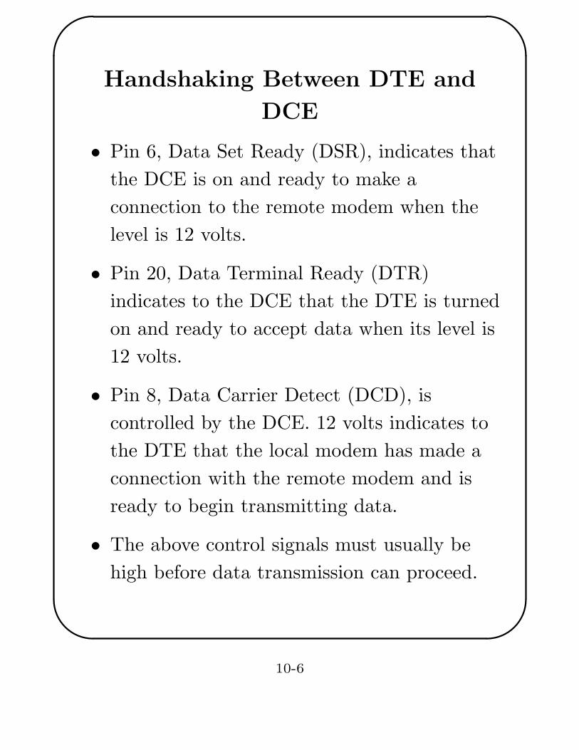
Binary Signaling on the Additive,
White, Gaussian Noise Channel
Filter
Matched
Binary
Source
����-
?
��
-
�
Signal
Selector
s(t)
v(t)
r(t)Slicer
d̂n rn
dn
+
dn is the transmitted binary data sequence
s(t) =∑
n
anp(t− nT ) is the transmitted signal
an =
A for dn = 0
−A for dn = 1
10-9

'
&
$
%
Binary Signaling (cont.)
p(t) =
1 for 0 ≤ t < T
0 elsewhere
v(t) is white, Gaussian noise with power spectrum
S(ω) = N0/2 and autocorrelation function
R(τ) = N0
2 δ(τ)
The Received Signal
r(t) = s(t) + v(t)
The Matched Filter Output
rn =1
T
(n+1)T∫
nT
r(t) dt =1
T
(n+1)T∫
nT
an + v(t) dt
= an +1
T
(n+1)T∫
nT
v(t) dt = an + vn
10-10
'
&
$
%
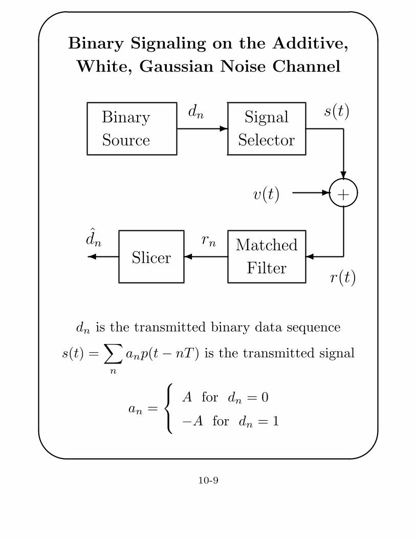
Binary Signaling (cont.)
Expected Value of Output Noise
E{vn} =1
T
∫ (n+1)T
nT
E{v(t)} dt = 0
Variance of the Output Noise
σ2 = E{v2n} = E
1
T
(n+1)T∫
nT
v(t) dt
2
=1
T 2
(n+1)T∫
nT
(n+1)T∫
nT
E{v(t)v(τ)} dt dτ
=1
T 2
(n+1)T∫
nT
(n+1)T∫
nT
N0
2δ(t− τ) dt dτ
=1
T 2
(n+1)T∫
nT
N0
2dτ =
N0
2T
10-11

'
&
$
%
Bit-Error Probability for Binary
Signaling
Assume an = −A. Then rn is a Gaussian random
variable with mean −A and variance σ2. The
error probability is
P (error |an = −A) = P (rn > 0 | an = −A)
= P (−A+ vn > 0) = P
(
vnσ
>A
σ
)
The random variable vn/σ is a Gaussian random
variable with zero mean and variance 1.
Therefore,
P (error |an = −A) =
∞∫
A/σ
1√2π
e−v2
2 dv = Q(A/σ)
where
Q(x) =
∫ ∞
x
1√2π
e−v2
2 dv
10-12

'
&
$
%
Error Probability (cont.)
Physical Significance of A/σ
• The signal component of the matched filter
output has power Ps = A2
• The noise component of the matched filter
output has power Pv = σ2
• The signal-to-noise ratio (SNR) at the
matched filter output is
ρ = SNR =Ps
Pv=
A2
σ2
Thus
A
σ=
√ρ =
√
2A2T
N0=
√
2EbN0
where Eb = A2T is the transmitted energy per bit.
Therefore
P (error |an = −A) = Q(√ρ)
10-13

'
&
$
%
Error Probability (cont.)
By similar analysis it can be shown that
P (error |an = A) = P (error |an = −A)
Thus, the average error probability is
Pe = P (an = −A)P (error |an = −A)
+ P (an = A)P (error |an = A)
= Q(√ρ)
An Approxiation for the Error Probability
Pe can be accurately approximated for√ρ greater
than 2 by
Pe =
∞∫
√ρ
1√2π
e−v2
2 dv ≃ 1√2πρ
e−ρ
2
This is actually an upper bound and becomes
more accurate as√ρ increases.
10-14

'
&
$
%
The Power Spectral Density
If the analog levels, an, have zero mean, constant
power Ps = E{a2n}, and the levels in different bit
intervals are statistically independent, the power
spectral density for the transmitted signal is
S(ω) =Ps
T|P (ω)|2 (1)
where
P (ω) =
∫ ∞
−∞
p(t)e−jωt dt (2)
For rectangular pulses of height 1 and Ps = A2
P (ω) =1− e−jωT
jω= Te−jω T
2
ejωT2 − e−jω T
2
2jω T2
= Te−jω T2
sinω T2
ω T2
(3)
Therefore, the power spectral density is
S(ω) = A2T
(
sinω T2
ω T2
)2
(4)
10-15
'
&
$
%
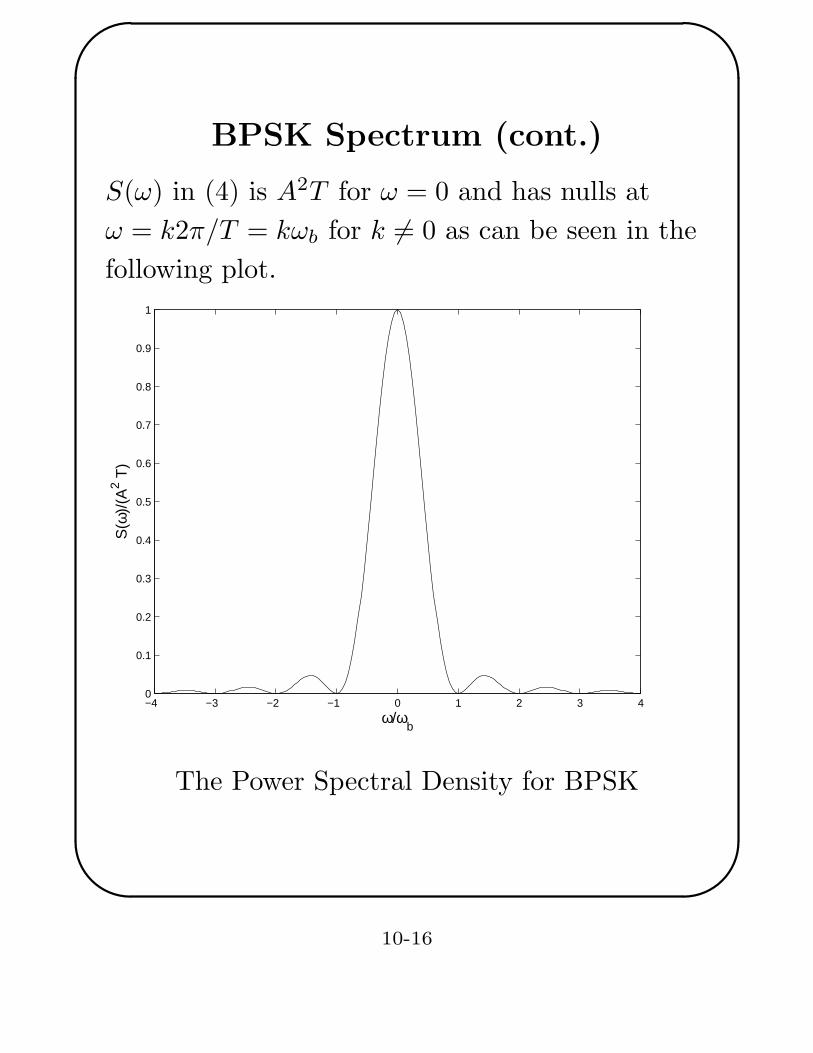
BPSK Spectrum (cont.)
S(ω) in (4) is A2T for ω = 0 and has nulls at
ω = k2π/T = kωb for k 6= 0 as can be seen in the
following plot.
−4 −3 −2 −1 0 1 2 3 40
0.1
0.2
0.3
0.4
0.5
0.6
0.7
0.8
0.9
1
ω/ωb
S(ω
)/(A
2 T)
The Power Spectral Density for BPSK
10-16

'
&
$
%
Generating Gaussian Random
Numbers
Pairs of independent, zero mean, Gaussian
random numbers can be generated by the
following steps:
1. Generate Random Numbers Uniform
Over [0,1)
• rand(void) generates integers uniformly
distributed over [0,RAND MAX] where
RAND MAX = 32767 = 215 − 1.
• srand(unsigned int seed) sets the value of
the random number generator seed so that
subsequent calls of rand produce a new
sequence of pseudorandom numbers.
srand does not return a value.
• If rand is called before srand is called, a
seed value of 1 is used.
10-17

'
&
$
%
Gaussian RV’s (cont. 1)
Sample Code for Generating Uniform
[0,1) RV’s
float v;
v = (float) rand()/(RAND_MAX + 1);
2. Converting a Uniform to a Rayleigh
Random Variable
A Rayleigh random variable, R, has the pdf
fR(r) =r
σ2e−
r2
2σ2 u(r)
and cumulative distribution function
FR(r) =
[
1− e−r2
2σ2
]
u(r)
10-18

'
&
$
%
Gaussian RV’s (cont. 2)
Let v =
[
1− e−r2
2σ2
]
u(r). Then, for
0 ≤ v < 1, the inverse cdf is
r = F−1R (v) =
√
−2σ2 loge(1− v)
Now let V be a random variable uniform over
[0,1). Then
R =√
−2σ2 loge(1− V )
is a Rayleigh random variable.
3. Transforming a Rayleigh RV into an
Independent Pair of Gaussian RV’s
Let Θ be a random variable uniformly
distributed over [0, 2π) and independent of V .
Then
X = R cosΘ and Y = R sinΘ
are two independent Gaussian random
10-19

'
&
$
%
variables, each with zero mean and variance
σ2. That is, they each have the pdf
f(x) =1
σ√2π
e−x2
2σ2
Navtel Bit Error Rate Tester
• Can act as a DCE or DTE in full duplex
mode.
• Data rates from 50 bps to 64 kbps.
• It performs a BERT test by transmitting a
specified pattern and assumes the same
pattern is transmitted from the remote end.
It synchronizes to the received pattern and
then counts errors.
Test patterns include:
– Several ASCII text sequences
– PN sequences of length 63, 511, 2047, and
4095.
10-20

'
&
$
%
Navtel BERT (cont.)
During the test, the Navtel counts the number
of bits received and the number of errors and
continually computes the bit-error rate as the
ratio of the current cumulative number of
errors and the number of bits received.
• The Navtel has a full RS-232C breakout box.
– Each key lead has a red and green LED
monitor.
– An illuminated red LED indicates an ON,
space, or 12 volt signal.
– An illuminated green LED indicates an
OFF, mark, or -12 volt signal.
– Neither LED is illuminated if the level is
between -3 and 3 volts.
– It can be connected between a DTE and
DCE to monitor the leads.
10-21

'
&
$
%
RS232 to TTL Level Conversion
• In this experiment, McBSP1 of the
TMS320C6713 will be used to exchange serial
data with the NAVTEL. The pins of this port
are brought out through a MAXIM MAX238
TTL/RS232 converter to a DB25 RS232
connector on the bracket next to the EVM
bracket.
• The NAVTEL will act as a DTE (terminal)
and the ’C6713 as a DCE (modem).
• A TTL to RS232 converter is required since
RS232 levels are 12 and -12 volts and the
corresponding TTL levels are 0 and 5 volts.
A logical 0 corresponds to the 0 volt TTL
level or 12 volt RS232 level. A block diagram
of the coverter configuration is shown in the
next slide.
10-22

'
&
$
%
TTL to RS232 Converter
Voltage Inverter
8.3v+
+5v
+5v
+5v
+5v
+
16v
Vcc
+5v to +10v+
+
GND
5
18
19
21
T1out
T2out
T3out
T4out
R3in
R4in
R2in
R1in
22
17
8
14
13
12
109
11
15
Receiver Clock
Data Set Ready
2
1
24
20
7
3
23
16
Transmitted Data
MAXIM MAX238 Data Carrier Detect
Data Terminal Ready
T1in
T2in
T3in
T4in
R1out
R2out
R3out
R4out
Voltage Doubler
Signal Ground
Transmitter Clock
Clear to Send
RS−232 Drivers/Receivers
Request to Send
Received Data
6
4
9
Expansion Peripheral opto oupler HCPL-2601
+5 v
Interfa e Conne tor
C2+ 10�fC1+ V+C2� V�
DB25 RS-232 Conne torDSR 6
TC 15TD 2RC 17
+10v to �10v
SG 7
10�f
DTR 20RTS 4CTS 5DCD 8
RD 3C1�
36 XDX1
45 TOUT032 GND
42 XDR139 XCLKR1
34 XCLKS1
33 XCLKX14:7�f16v8.3v4:7�f
10-23

'
&
$
%
Why We are Using McBSP1 Instead
of McBSP0
The lab textbook describes using McBSP0 for this
chapter rather than McBSP1. Ideally McBSP0
should be used with the TMS320C6713 DSK.
McBSP0 is normally used as the control channel
for the AIC23 codec. Using it for this experiment
would allow McBSP1 to still be used for sending
and receiving data samples from the codec. Then
serial data could be input and output with
McBSP0, and the DSK could be programmed to
be a modem with transmit and receive samples
interfaced with the codec through McBSP1.
The TTL/RS232 daughter cards on our C6713
DSK’s were taken from our previously used C6701
EVM’s. McBSP1 was used as the codec control
port and McBSP0 as the data sample port on the
C6701 EVM. We decided not to make new
daughter cards. Fortunately, the daughter card
connectors have the same pin functions on the
EVM and DSK.
10-24

'
&
$
%
Setting Timer 0 and McBSP1
The sample rate generator (SRG) in McBSP1 will
be used to generate the
• transmit frame sync (FSX)
• receive frame sync (FSR)
• transmit bit clock (CLKX)
• receive bit clock (CLKR)
The frame syncs FSR and FSX are not connected
to the Navtel tester but are used internally in
McBSP1.
The bit clocks CLKR and CLKX are connected
to the Navtel tester and used as its external data
clocks, so McBSP1 must be configured to make
them outputs.
10-25

'
&
$
%
Setting Timer 0
Select the clock for the sample rate generator as
an external clock supplied by timer 0. The timer
output, TOUT0, is looped back to the SRG1 clock
input pin, CLKS1, by the TTL/RS232 converter.
• The formula for the frequency of TOUT in
clock mode (50% duty cycle) is:
fTOUT =CPU clock frequency
8× Period Register value
where the Period Register value is an
unsigned 32-bit integer.
The CPU clock frequency is 225 MHz for the
’C6713 DSK
• Block diagrams of the Sample Rate Generator
and and McBSP clock generation circuit are
shown on Slide 10-28.
10-26

'
&
$
%
Reason for Using TOUT0 as the
Clock
• See Chapter 12, TMS320C6000 Peripherals
Reference Guide for complete details on the
serial ports and their sample rate generator
and clock generator circuitry.
• You will notice there that the SRG can use
an internal clock whose frequency is:
– CPU clock for the ’C6701
– CPU clock/2 for the ’C6713
and that the clock generation circuitry has
dividers to generate the bit clocks and frame
syncs.
• The reason for choosing TOUT0 as the clock
source is that the dividers in the SRG cannot
divide the internal clock by a large enough
factor to achieve the desired 19200 bps rate.
10-27

'
&
$
%
Sample Rate Generator and McBSP Clock
GenerationFigure 12–37. Sample Rate Generator
CLKS
CLKSP
FSR
GSYNC
FSG
CLKGCLKSM
CLKGDV FPER FWID
pulseFrame
synchronizationand clockdetection
Frame pulse
internal clock source†
1
0
CLKSRG
† Internal clock source: CPU clock for C620x/C670x CPU/2 clock for C621x/C671x CPU/4 clock for C64x.
Figure 12–36. Clock and Frame Generation
0
1
1
0
CLKXM
0
1
Inset:
FSX pin
FSR pinCLKR pin
CLKX pin
FSG
FSX_intCLKX_int
Frame selectionClock selection
(R/X) IOEN
CLKG
FSR_intCLKS pin
internal clock source†
DXR to XSR
FSGM
0
1
FSR_intCLKR_int
FSRP
1
0 0
1
FSRM
FSRM & GSYNCFSRP
0
1FSXP
See inset
FSXP
FSXM
FSXM
generator
Samplerate
Receive
Transmit
DLBCLKRM
CLKRM
CLKXM
CLKRP
CLKRP
CLKXP
CLKXP
See inset
See inset See inset
Yyy_int
DLB
† Internal clock source: CPU clock for C620x/C670x CPU/2 clock for C621x/C671x CPU/4 clock for C64x.
10-28

'
&
$
%
Bit Clocks and Frame Sync’s
• To configure the McBSP1 sample rate
generator to use TOUT0 as its clock, set the
clock select mode bit (CLKSM) to 0. TOUT0
can be inverted in the SRG according to the
value of CLKSP resulting in CLKSRG.
• The clock, CLKSRG, is applied to a first
divider which uses the value of the 8-bit
unsigned integer, CLKGDV, as the
divide-down number to generate the signal,
CLKG which is possibly inverted to form the
bit clocks CLKX and CLKR. The bit clocks
have a 50% duty cycle when CLKGDV is odd
or 0.
• The frequency of CLKG when TIMER 0 is in
clock mode is
CLKG frequency =CLKSRG frequency
CLKGDV + 1
=CPU clock frequency
8× (Period Register)(CLKGDV+ 1)
10-29

'
&
$
%
Bit Clocks and Frame Sync’s (cont. 1)
• CLKG is then applied to a divider with the
unsigned integer 12-bit divide-down number,
FPER, to generate the signal FSG which is at
the frame sync frequency. The frequency of
FSG is
frame sync frequency = FSG frequency
=CLKG frequency
FPER + 1
• The sample rate generator includes one
additional counter to generate the width of
the frame sync pulse. The unsigned 8-bit
integer, FWID, determines the frame sync
pulse width. The FSG pulse width is
FWID + 1 pulses of CLKG.
The following slides show how to initialize the
Chip Support Library McBSP configuration
structure for the desired mode of operation.
10-30

'
&
$
%
Initializing the McBSP1
Configuration Structure
The detailed descriptions of the mnemonics used
in the following structures for initializing McBSP1
and Timer0 can be found in SPRU401 TMS6000
Chip Support Library API Reference Guide.
• McBSP1 is configured to transmit and receive
32-bit words.
• The divide-down number, FPER, for the
frame syncs is set to 31. The actual frame
sync period will be FPER + 1 = 32 serial bit
clocks. Then data bits are transmitted and
received with no gaps between words.
• The start of bits received at RSR1 should be
aligned with the rising edge of CLKR1. The
start of bits sent from XSR1 should be
aligned with the rising edge of CLKX1. The
NAVTEL box samples received bits at the
falling edge of CLKX1 which is in the center
of the bit.
10-31

'
&
$
%
McBSP1 Configuration Structure
MCBSP_Config mcbspCfgData = {
MCBSP_FMKS(SPCR, FREE, NO) |
MCBSP_FMKS(SPCR, SOFT, NO) |
MCBSP_FMKS(SPCR, FRST, NO) |
MCBSP_FMKS(SPCR, GRST, YES) |
MCBSP_FMKS(SPCR, XINTM, XRDY) |
MCBSP_FMKS(SPCR, XSYNCERR, NO) |
MCBSP_FMKS(SPCR, XRST, YES) |
MCBSP_FMKS(SPCR, DLB, OFF) |
MCBSP_FMKS(SPCR, RJUST, RZF) |
MCBSP_FMKS(SPCR, CLKSTP, DISABLE) |
MCBSP_FMKS(SPCR, DXENA, OFF) |
MCBSP_FMKS(SPCR, RINTM, RRDY) |
MCBSP_FMKS(SPCR, RSYNCERR, NO) |
MCBSP_FMKS(SPCR, RRST, YES),
MCBSP_FMKS(RCR, RPHASE, SINGLE) |
MCBSP_FMKS(RCR, RFRLEN2, OF(0)) |
MCBSP_FMKS(RCR, RWDLEN2, DEFAULT) |
MCBSP_FMKS(RCR, RCOMPAND, MSB) |
MCBSP_FMKS(RCR, RFIG, NO) |
MCBSP_FMKS(RCR, RDATDLY, 0BIT) |
MCBSP_FMKS(RCR, RFRLEN1, OF(0)) |
MCBSP_FMKS(RCR, RWDLEN1, 32BIT) |
MCBSP_FMKS(RCR, RWDREVRS, DISABLE),
10-32

'
&
$
%
McBSP1 Configuration Structure (cont. 1)
MCBSP_FMKS(XCR, XPHASE, SINGLE) |
MCBSP_FMKS(XCR, XFRLEN2, DEFAULT) |
MCBSP_FMKS(XCR, XWDLEN2, DEFAULT) |
MCBSP_FMKS(XCR, XCOMPAND, MSB) |
MCBSP_FMKS(XCR, XFIG, NO) |
MCBSP_FMKS(XCR, XDATDLY, 0BIT) |
MCBSP_FMKS(XCR, XFRLEN1, OF(0)) |
MCBSP_FMKS(XCR, XWDLEN1, 32BIT) |
MCBSP_FMKS(XCR, XWDREVRS, DISABLE),
MCBSP_FMKS(SRGR, GSYNC, FREE) |
MCBSP_FMKS(SRGR, CLKSP, RISING) |
MCBSP_FMKS(SRGR, CLKSM, CLKS) |
MCBSP_FMKS(SRGR, FSGM, FSG) |
MCBSP_FMKS(SRGR, FPER, OF(31)) |
MCBSP_FMKS(SRGR, FWID, OF(1)) |
MCBSP_FMKS(SRGR, CLKGDV, OF(0)),
MCBSP_MCR_DEFAULT,
MCBSP_RCER_DEFAULT,
MCBSP_XCER_DEFAULT,
MCBSP_FMKS(PCR, XIOEN, SP) |
MCBSP_FMKS(PCR, RIOEN, SP) |
MCBSP_FMKS(PCR, FSXM, INTERNAL) |
MCBSP_FMKS(PCR, FSRM, INTERNAL) |
MCBSP_FMKS(PCR, CLKXM, OUTPUT) |
MCBSP_FMKS(PCR, CLKRM, OUTPUT) |
MCBSP_FMKS(PCR, CLKSSTAT, DEFAULT) |
MCBSP_FMKS(PCR, DXSTAT, DEFAULT) |
10-33

'
&
$
%
McBSP1 Configuration Structure ( cont. 2)
MCBSP_FMKS(PCR, FSXP, ACTIVEHIGH) |
MCBSP_FMKS(PCR, FSRP, ACTIVEHIGH) |
MCBSP_FMKS(PCR, CLKXP, RISING) |
MCBSP_FMKS(PCR, CLKRP, FALLING)
};
Configuring Timer 0
The following code segment shows how to
configure and start the timer using the Chip
Support Library.
...
unsigned int period_reg;
unsigned int ctrl_reg = 0;
unsigned int cnt = 0; /* Initial counter value */
int chan = 0;
period_reg = ‘‘You compute the required value.’’;
/**********************************************************/
/* Set the Timer Control Register (CTL) so that: */
/* Bit 0, FUNC = 1, TOUT is timer output pin */
/* Bit 8, C_P = 1, clock mode (50% duty cycle) */
/* Bit 9, CLKSRC = 1, Internal clock source, CPU clock/4 */
/**********************************************************/
ctrl_reg = MASK_BIT(C_P)|MASK_BIT(CLKSRC)|MASK_BIT(FUNC);
TIMER_INIT(chan,ctrl_reg,period_reg,cnt);
TIMER_START(chan);
...
10-34

'
&
$
%
Laboratory Experiments
1. Connect the DCE socket of the Navtel tester
to the DB25 RS232 connector at the bottom
rear of the PC.
2. Turn on the Navtel tester and press the right
and left arrows until BERT blinks. Then
press SETUP/CLEAR. Now set the Navtel
parameters as follows:
(a) Press the right arrow to make the entry
under MESSAGE blink and then press
SETUP. Use the arrows to select 4095 and
press SETUP again. This selects the shift
register sequence of length 4095.
(b) Similarly, set the message length to Cont
(continuous).
(c) Set CLOCK to Ext (external). The clocks
will be generated by the DSP’s serial port
McBSP1 and converted to RS-232C levels
by the converter card.
10-35

'
&
$
%
Experiments (cont. 1)
(d) Set the MODE to DTE so the Navtel
looks like a terminal (DTE).
(e) Set the LEVEL to 8 and PARITY to No.
This means that in the async mode each
character will consist of 8 data bits with
no parity bit.
(f) Set SY/ASY to Syn (synchronous). In this
mode, a continuous bit stream with no
start and stop bits is transmitted.
(g) Set the SPEED to 19200.
3. Write a program for the DSP to take bits
from the Navtel tester and simply loop them
back to the Navtel through McBSP1. Later
you will be asked to introduce errors into the
bit stream. The sample rate generator (SRG)
in McBSP1 should be used to generate the bit
clocks and frame sync’s as explained
previously.
10-36

'
&
$
%
Experiments (cont. 2)
Your program must connect the McBSP1 pins
to the peripheral expansion connector for the
daughter card. You can do this by using the
BSL function
DSK6713_rset(DSK6713_MISC, 0x02);
To see BSL documentation, double click on
C:\CCStudio_v3.1\docs\hlp\c6713dsk.hlp
and look at the “Board Support Library”
topic. Also see the TMS320C6713 DSK
Technical Reference manual.
4. Select the timer Period Register for sample
rate generator divider CLKGDV= 0 to give a
serial bit rate as close to 19200 bps as
possible.
• Check your initial program by starting a
bit-error rate test. To do this, press RUN
on the Navtel tester. Press the up or down
arrows until BERT is displayed. If you are
looping the data back correctly, BERT
should remain 0.
10-37

'
&
$
%
Experiments (cont. 3)
• You can introduce a single error by pressing
INSERT ERROR and observe the effect on
the BERT display.
5. Now modify your program to add errors to
the bit stream.
• For each of the 16 pairs of bits in a received
32-bit word, generate a pair of zero mean,
uncorrelated, Gaussian noise samples by the
method described in Slides 10-17 through
10-20.
• Assume that a logical 0 is represented by A
volts on the channel and logical 1 by −A
volts. Let the integrator output noise
variance be σ2 = 1 and adjust A to get the
desired output signal-to-noise ratio. Then,
the SNR in dB is
S = 10 log10A2
σ2= 20 log10 A
10-38

'
&
$
%
Experiments (cont. 4)
and the required value for A is
A = 10S/20
• Let a particular pair of Gaussian noise
samples be denoted by (x, y). According to
the theory, a transmitted 1 is changed
to a 0 if x > A and a transmitted 0 is
changed to a 1 if x ≤ −A. The probabilities
of these two events are identical because the
probability density function for the zero
mean, Gaussian random variables is even.
To determine when to introduce a bit error,
check to see if x > A. If this is true, an error
should be introduced in the first bit of a pair.
Similarly, when y > A an error should be
introduced in the second bit of a pair.
10-39

'
&
$
%
Experiments (cont. 5)
The errors can be introduced by XOR-ing 1’s
into the error locations in the received 32-bit
serial word to complement the correct bits.
6. Now experimentally generate a bit-error rate
vs. SNR plot. Start with a 15 dB SNR and
work down to 7 dB in 0.5 dB increments.
Make sure to run your test long enough at
each SNR to obtain a statistically reliable
estimate of the error rate. Plot the BER as
the ordinate on a logarithmic scale. Plot the
SNR in dB on a linear dB scale.
7. Theoretically compute the BER vs. SNR plot
and compare it with your experimentally
measured curve.
10-40

'
&
$
%
The Complementary Error Function
erfc(x) vs. Q(x)
In mathematics texts and MATLAB, the
complementary error function is defined as
erfc(x) =2√π
∫ ∞
x
e−t2 dt
The tail probability for a standard normal random
variable (Gaussian with 0 mean and variance 1) is
Q(x) =1√2π
∫ ∞
x
e−u2/2 du
Making the substitution u/√2 = t in the intergral
for Q(x) gives
Q(x) =1
2erfc
(
x√2
)
You can use this result in MATLAB to compute
the theoretical bit-error probability.
10-41
Related Documents