Chapter 1 Solutions 2 Chapter 2 Solutions 6 Chapter 3 Solutions 13 Chapter 4 Solutions 33 Chapter 5 Solutions 44 Chapter 6 Solutions 50 Appendix A Solutions 63 Appendix B Solutions 83 Appendix C Solutions 92 Copyright © 2012 Elsevier, Inc. All rights reserved.

Welcome message from author
This document is posted to help you gain knowledge. Please leave a comment to let me know what you think about it! Share it to your friends and learn new things together.
Transcript

Chapter 1 Solutions 2
Chapter 2 Solutions 6
Chapter 3 Solutions 13
Chapter 4 Solutions 33
Chapter 5 Solutions 44
Chapter 6 Solutions 50
Appendix A Solutions 63
Appendix B Solutions 83
Appendix C Solutions 92
Copyright © 2012 Elsevier, Inc. All rights reserved.

Solutions to Case Studies
and Exercises 1
Copyright © 2012 Elsevier, Inc. All rights reserved.
2 ■ Solutions to Case Studies and Exercises
Case Study 1: Chip Fabrication Cost 1
1.1 a.
b. It is fabricated in a larger technology, which is an older plant. As plants age,their process gets tuned, and the defect rate decreases.
1.2 a.
Profit = 416 × 0.65 × $20 = $5408
b.
Profit = 240 × 0.50 × $25 = $3000
c. The Woods chip
d. Woods chips: 50,000/416 = 120.2 wafers neededMarkon chips: 25,000/240 = 104.2 wafers needed
Therefore, the most lucrative split is 120 Woods wafers, 30 Markon wafers.
1.3 a.
No defects = 0.282 = 0.08One defect = 0.28 × 0.72 × 2 = 0.40No more than one defect = 0.08 + 0.40 = 0.48
b.
$20 × 0.28 = Wafer size/old dpw
= $23.33
Chapter 1 Solutions
Yield 10.30 3.89×
4.0---------------------------+⎝ ⎠
⎛ ⎞4–
0.36= =
Dies per waferπ 30 2⁄( )× 2
1.5-----------------------------=
π 30×sqrt 2 1.5×( )-------------------------------– 471 54.4 416=–=
Yield 10.30 1.5×
4.0------------------------+⎝ ⎠
⎛ ⎞4–
0.65= =
Dies per waferπ 30 2⁄( )× 2
2.5-----------------------------=
π 30×sqrt 2 2.5×( )-------------------------------– 283 42.1 240=–=
Yield 10.30 2.5×
4.0--------------------------+⎝ ⎠
⎛ ⎞4–
0.50= =
Defect – Free single core 10.75 1.99 2⁄×
4.0----------------------------------+⎝ ⎠
⎛ ⎞4–
0.28= =
$20Wafer size
old dpw 0.28×------------------------------------=
xWafer size
1/2 old dpw× 0.48×--------------------------------------------------$20 0.28×1/2 0.48×-------------------------= =
Copyright © 2012 Elsevier, Inc. All rights reserved.

Chapter 1 Solutions ■ 3
Case Study 2: Power Consumption in Computer Systems
1.4 a. .80x = 66 + 2 × 2.3 + 7.9; x = 99
b. .6 × 4 W + .4 × 7.9 = 5.56
c. Solve the following four equations:
seek7200 = .75 × seek5400seek7200 + idle7200 = 100seek5400 + idle5400 = 100seek7200 × 7.9 + idle7200 × 4 = seek5400 × 7 + idle5400 × 2.9
idle7200 = 29.8%
1.5 a.
b.
c. 200 W × 11 = 2200 W2200/(76.2) = 28 racksOnly 1 cooling door is required.
1.6 a. The IBM x346 could take less space, which would save money in real estate.The racks might be better laid out. It could also be much cheaper. In addition,if we were running applications that did not match the characteristics of thesebenchmarks, the IBM x346 might be faster. Finally, there are no reliabilitynumbers shown. Although we do not know that the IBM x346 is better in anyof these areas, we do not know it is worse, either.
1.7 a. (1 – 8) + .8/2 = .2 + .4 = .6
b.
c. ; x = 50%
d.
Exercises
1.8 a. (1.35)10 = approximately 20
b. 3200 × (1.4)12 = approximately 181,420
c. 3200 × (1.01)12 = approximately 3605
d. Power density, which is the power consumed over the increasingly small area,has created too much heat for heat sinks to dissipate. This has limited theactivity of the transistors on the chip. Instead of increasing the clock rate,manufacturers are placing multiple cores on the chip.
14 KW66 W 2.3 W 7.9 W+ +( )------------------------------------------------------------ 183=
14 KW66 W 2.3 W 2+ + 7.9 W×( )--------------------------------------------------------------------- 166=
Power newPower old--------------------------
V 0.60×( )2F 0.60×( )×
V2
F×----------------------------------------------------------- 0.63 0.216= = =
1.75
1 x–( ) x 2⁄+--------------------------------=
Power newPower old--------------------------
V 0.75×( )2 F 0.60×( )×V2 F×
----------------------------------------------------------- 0.752 0.6× 0.338= = =
Copyright © 2012 Elsevier, Inc. All rights reserved.

4 ■ Solutions to Case Studies and Exercises
e. Anything in the 15–25% range would be a reasonable conclusion based onthe decline in the rate over history. As the sudden stop in clock rate shows,though, even the declines do not always follow predictions.
1.9 a. 50%
b. Energy = ½ load × V2. Changing the frequency does not affect energy–onlypower. So the new energy is ½ load × ( ½ V)2, reducing it to about ¼ the oldenergy.
1.10 a. 60%
b. 0.4 + 0.6 × 0.2 = 0.58, which reduces the energy to 58% of the originalenergy.
c. newPower/oldPower = ½ Capacitance × (Voltage × .8)2 × (Frequency × .6)/ ½Capacitance × Voltage × Frequency = 0.82 × 0.6 = 0.256 of the original power.
d. 0.4 + 0 .3 × 2 = 0.46, which reduce the energy to 46% of the original energy.
1.11 a. 109/100 = 107
b. 107/107 + 24 = 1
c. [need solution]
1.12 a. 35/10000 × 3333 = 11.67 days
b. There are several correct answers. One would be that, with the current sys-tem, one computer fails approximately every 5 minutes. 5 minutes is unlikelyto be enough time to isolate the computer, swap it out, and get the computerback on line again. 10 minutes, however, is much more likely. In any case, itwould greatly extend the amount of time before 1/3 of the computers havefailed at once. Because the cost of downtime is so huge, being able to extendthis is very valuable.
c. $90,000 = (x + x + x + 2x)/4$360,000 = 5x$72,000 = x4th quarter = $144,000/hr
1.13 a. Itanium, because it has a lower overall execution time.
b. Opteron: 0.6 × 0.92 + 0.2 × 1.03 + 0.2 × 0.65 = 0.888
c. 1/0.888 = 1.126
1.14 a. See Figure S.1.
b. 2 = 1/((1 – x) + x /10)5/9 = x = 0.56 or 56%
c. 0.056/0.5 = 0.11 or 11%
d. Maximum speedup = 1/(1/10) = 105 = 1/((1 – x) + x /10)8/9 = x = 0.89 or 89%
Copyright © 2012 Elsevier, Inc. All rights reserved.

Chapter 1 Solutions ■ 5
e. Current speedup: 1/(0.3 + 0.7/10) = 1/0.37 = 2.7Speedup goal: 5.4 = 1/((1 – x) + x /10) = x = 0.91
This means the percentage of vectorization would need to be 91%
1.15 a. old execution time = 0.5 new + 0.5 × 10 new = 5.5 new
b. In the original code, the unenhanced part is equal in time to the enhanced partsped up by 10, therefore:(1 – x) = x /1010 – 10x = x10 = 11x10/11 = x = 0.91
1.16 a. 1/(0.8 + 0.20/2) = 1.11
b. 1/(0.7 + 0.20/2 + 0.10 × 3/2) = 1.05
c. fp ops: 0.1/0.95 = 10.5%, cache: 0.15/0.95 = 15.8%
1.17 a. 1/(0.6 + 0.4/2) = 1.25
b. 1/(0.01 + 0.99/2) = 1.98
c. 1/(0.2 + 0.8 × 0.6 + 0.8 × 0.4/2) = 1/(.2 + .48 + .16) = 1.19
d. 1/(0.8 + 0.2 × .01 + 0.2 × 0.99/2) = 1/(0.8 + 0.002 + 0.099) = 1.11
1.18 a. 1/(.2 + .8/N)
b. 1/(.2 + 8 × 0.005 + 0.8/8) = 2.94
c. 1/(.2 + 3 × 0.005 + 0.8/8) = 3.17
d. 1/(.2 + logN × 0.005 + 0.8/N)
e. d/dN(1/((1 – P) + logN × 0.005 + P/N)) = 0
Figure S.1 Plot of the equation: y = 100/((100 – x) + x/10).
0 10 20 30 40 50
Percent vectorization
Net
spe
edup
60 70 80 90 100
12
10
8
6
4
2
0
Copyright © 2012 Elsevier, Inc. All rights reserved.

6 ■ Solutions to Case Studies and Exercises
Case Study 1: Optimizing Cache Performance via Advanced Techniques
2.1 a. Each element is 8B. Since a 64B cacheline has 8 elements, and each columnaccess will result in fetching a new line for the non-ideal matrix, we need aminimum of 8x8 (64 elements) for each matrix. Hence, the minimum cachesize is 128 × 8B = 1KB.
b. The blocked version only has to fetch each input and output element once.The unblocked version will have one cache miss for every 64B/8B = 8 rowelements. Each column requires 64Bx256 of storage, or 16KB. Thus, columnelements will be replaced in the cache before they can be used again. Hencethe unblocked version will have 9 misses (1 row and 8 columns) for every 2 inthe blocked version.
c. for (i = 0; i < 256; i=i+B) {for (j = 0; j < 256; j=j+B) {
for(m=0; m<B; m++) {for(n=0; n<B; n++) {
output[j+n][i+m] = input[i+m][j+n];
}
}
}
}
d. 2-way set associative. In a direct-mapped cache the blocks could be allocatedso that they map to overlapping regions in the cache.
e. You should be able to determine the level-1 cache size by varying the blocksize. The ratio of the blocked and unblocked program speeds for arrays thatdo not fit in the cache in comparison to blocks that do is a function of thecache block size, whether the machine has out-of-order issue, and the band-width provided by the level-2 cache. You may have discrepancies if yourmachine has a write-through level-1 cache and the write buffer becomes alimiter of performance.
2.2 Since the unblocked version is too large to fit in the cache, processing eight 8B ele-ments requires fetching one 64B row cache block and 8 column cache blocks.Since each iteration requires 2 cycles without misses, prefetches can be initiatedevery 2 cycles, and the number of prefetches per iteration is more than one, thememory system will be completely saturated with prefetches. Because the latencyof a prefetch is 16 cycles, and one will start every 2 cycles, 16/2 = 8 will be out-standing at a time.
2.3 Open hands-on exercise, no fixed solution.
Chapter 2 Solutions
Copyright © 2012 Elsevier, Inc. All rights reserved.

Chapter 2 Solutions ■ 7
Case Study 2: Putting it all Together: Highly Parallel Memory Systems
2.4 a. The second-level cache is 1MB and has a 128B block size.
b. The miss penalty of the second-level cache is approximately 105ns.
c. The second-level cache is 8-way set associative.
d. The main memory is 512MB.
e. Walking through pages with a 16B stride takes 946ns per reference. With 250such references per page, this works out to approximately 240ms per page.
2.5 a. Hint: This is visible in the graph above as a slight increase in L2 miss servicetime for large data sets, and is 4KB for the graph above.
b. Hint: Take independent strides by the page size and look for increases inlatency not attributable to cache sizes. This may be hard to discern if theamount of memory mapped by the TLB is almost the same as the size as acache level.
c. Hint: This is visible in the graph above as a slight increase in L2 miss servicetime for large data sets, and is 15ns in the graph above.
d. Hint: Take independent strides that are multiples of the page size to see if theTLB if fully-associative or set-associative. This may be hard to discern if theamount of memory mapped by the TLB is almost the same as the size as acache level.
2.6 a. Hint: Look at the speed of programs that easily fit in the top-level cache as afunction of the number of threads.
b. Hint: Compare the performance of independent references as a function oftheir placement in memory.
2.7 Open hands-on exercise, no fixed solution.
Exercises
2.8 a. The access time of the direct-mapped cache is 0.86ns, while the 2-way and4-way are 1.12ns and 1.37ns respectively. This makes the relative accesstimes 1.12/.86 = 1.30 or 30% more for the 2-way and 1.37/0.86 = 1.59 or59% more for the 4-way.
b. The access time of the 16KB cache is 1.27ns, while the 32KB and 64KB are1.35ns and 1.37ns respectively. This makes the relative access times 1.35/1.27 = 1.06 or 6% larger for the 32KB and 1.37/1.27 = 1.078 or 8% larger forthe 64KB.
c. Avg. access time = hit% × hit time + miss% × miss penalty, miss% = missesper instruction/references per instruction = 2.2% (DM), 1.2% (2-way), 0.33%(4-way), .09% (8-way).
Direct mapped access time = .86ns @ .5ns cycle time = 2 cycles2-way set associative = 1.12ns @ .5ns cycle time = 3 cycles
Copyright © 2012 Elsevier, Inc. All rights reserved.

8 ■ Solutions to Case Studies and Exercises
4-way set associative = 1.37ns @ .83ns cycle time = 2 cycles8-way set associative = 2.03ns @ .79ns cycle time = 3 cyclesMiss penalty = (10/.5) = 20 cycles for DM and 2-way; 10/.83 = 13 cycles for4-way; 10/.79 = 13 cycles for 8-way.
Direct mapped – (1 – .022) × 2 + .022 × (20) = 2.39 6 cycles => 2.396 × .5 = 1.2ns2-way – (1 – .012) × 3 + .012 × (20) = 3. 2 cycles => 3.2 × .5 = 1.6ns4-way – (1 – .0033) × 2 + .0033 × (13) = 2.036 cycles => 2.06 × .83 = 1.69ns8-way – (1 – .0009) × 3 + .0009 × 13 = 3 cycles => 3 × .79 = 2.37ns
Direct mapped cache is the best.
2.9 a. The average memory access time of the current (4-way 64KB) cache is 1.69ns. 64KB direct mapped cache access time = .86ns @ .5 ns cycle time = 2 cyclesWay-predicted cache has cycle time and access time similar to direct mappedcache and miss rate similar to 4-way cache.The AMAT of the way-predicted cache has three components: miss, hit withway prediction correct, and hit with way prediction mispredict: 0.0033 × (20)+ (0.80 × 2 + (1 – 0.80) × 3) × (1 – 0.0033) = 2.26 cycles = 1.13ns
b. The cycle time of the 64KB 4-way cache is 0.83ns, while the 64KB direct-mapped cache can be accessed in 0.5ns. This provides 0.83/0.5 = 1.66 or 66%faster cache access.
c. With 1 cycle way misprediction penalty, AMAT is 1.13ns (as per part a), butwith a 15 cycle misprediction penalty, the AMAT becomes: 0.0033 × 20 +(0.80 × 2 + (1 – 0.80) × 15) × (1 – 0.0033) = 4.65 cycles or 2.3ns.
d. The serial access is 2.4ns/1.59ns = 1.509 or 51% slower.
2.10 a. The access time is 1.12ns, while the cycle time is 0.51ns, which could bepotentially pipelined as finely as 1.12/.51 = 2.2 pipestages.
b. The pipelined design (not including latch area and power) has an area of1.19 mm2 and energy per access of 0.16nJ. The banked cache has an area of1.36 mm2 and energy per access of 0.13nJ. The banked design uses slightlymore area because it has more sense amps and other circuitry to support thetwo banks, while the pipelined design burns slightly more power because thememory arrays that are active are larger than in the banked case.
2.11 a. With critical word first, the miss service would require 120 cycles. Withoutcritical word first, it would require 120 cycles for the first 16B and 16 cyclesfor each of the next 3 16B blocks, or 120 + (3 × 16) = 168 cycles.
b. It depends on the contribution to Average Memory Access Time (AMAT) ofthe level-1 and level-2 cache misses and the percent reduction in miss servicetimes provided by critical word first and early restart. If the percentage reduc-tion in miss service times provided by critical word first and early restart isroughly the same for both level-1 and level-2 miss service, then if level-1misses contribute more to AMAT, critical word first would likely be moreimportant for level-1 misses.
Copyright © 2012 Elsevier, Inc. All rights reserved.

Chapter 2 Solutions ■ 9
2.12 a. 16B, to match the level 2 data cache write path.
b. Assume merging write buffer entries are 16B wide. Since each store canwrite 8B, a merging write buffer entry would fill up in 2 cycles. The level-2cache will take 4 cycles to write each entry. A non-merging write bufferwould take 4 cycles to write the 8B result of each store. This means themerging write buffer would be 2 times faster.
c. With blocking caches, the presence of misses effectively freezes progressmade by the machine, so whether there are misses or not doesn’t change therequired number of write buffer entries. With non-blocking caches, writes canbe processed from the write buffer during misses, which may mean fewerentries are needed.
2.13 a. A 2GB DRAM with parity or ECC effectively has 9 bit bytes, and wouldrequire 18 1Gb DRAMs. To create 72 output bits, each one would have tooutput 72/18 = 4 bits.
b. A burst length of 4 reads out 32B.
c. The DDR-667 DIMM bandwidth is 667 × 8 = 5336 MB/s.
The DDR-533 DIMM bandwidth is 533 × 8 = 4264 MB/s.
2.14 a. This is similar to the scenario given in the figure, but tRCD and CL areboth 5. In addition, we are fetching two times the data in the figure. Thus itrequires 5 + 5 + 4 × 2 = 18 cycles of a 333MHz clock, or 18 × (1/333MHz) =54.0ns.
b. The read to an open bank requires 5 + 4 = 9 cycles of a 333MHz clock, or27.0ns. In the case of a bank activate, this is 14 cycles, or 42.0ns. Including20ns for miss processing on chip, this makes the two 42 + 20 = 61ns and27.0 + 20 = 47ns. Including time on chip, the bank activate takes 61/47 = 1.30or 30% longer.
2.15 The costs of the two systems are $2 × 130 + $800 = $1060 with the DDR2-667DIMM and 2 × $100 + $800 = $1000 with the DDR2-533 DIMM. The latency toservice a level-2 miss is 14 × (1/333MHz) = 42ns 80% of the time and 9 × (1/333MHz) = 27ns 20% of the time with the DDR2-667 DIMM.
It is 12 × (1/266MHz) = 45ns (80% of the time) and 8 × (1/266MHz) = 30ns(20% of the time) with the DDR-533 DIMM. The CPI added by the level-2misses in the case of DDR2-667 is 0.00333 × 42 × .8 + 0.00333 × 27 × .2 = 0.130giving a total of 1.5 + 0.130 = 1.63. Meanwhile the CPI added by the level-2misses for DDR-533 is 0.00333 × 45 × .8 + 0.00333 × 30 × .2 = 0.140 giving atotal of 1.5 + 0.140 = 1.64. Thus the drop is only 1.64/1.63 = 1.006, or 0.6%,while the cost is $1060/$1000 = 1.06 or 6.0% greater. The cost/performance ofthe DDR2-667 system is 1.63 × 1060 = 1728 while the cost/performance of theDDR2-533 system is 1.64 × 1000 = 1640, so the DDR2-533 system is a bettervalue.
2.16 The cores will be executing 8cores × 3GHz/2.0CPI = 12 billion instructions persecond. This will generate 12 × 0.00667 = 80 million level-2 misses per second.With the burst length of 8, this would be 80 × 32B = 2560MB/sec. If the memory
Copyright © 2012 Elsevier, Inc. All rights reserved.
10 ■ Solutions to Case Studies and Exercises
bandwidth is sometimes 2X this, it would be 5120MB/sec. From Figure 2.14, thisis just barely within the bandwidth provided by DDR2-667 DIMMs, so just onememory channel would suffice.
2.17 a. The system built from 1Gb DRAMs will have twice as many banks as thesystem built from 2Gb DRAMs. Thus the 1Gb-based system should providehigher performance since it can have more banks simultaneously open.
b. The power required to drive the output lines is the same in both cases, but thesystem built with the x4 DRAMs would require activating banks on 18 DRAMs,versus only 9 DRAMs for the x8 parts. The page size activated on each x4 andx8 part are the same, and take roughly the same activation energy. Thus sincethere are fewer DRAMs being activated in the x8 design option, it would havelower power.
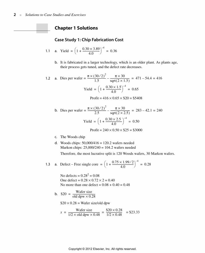
2.18 a. With policy 1,Precharge delay Trp = 5 × (1/333 MHz) = 15nsActivation delay Trcd = 5 × (1/333 MHz) = 15nsColumn select delay Tcas = 4 × (1/333 MHz) = 12nsAccess time when there is a row buffer hit
Access time when there is a miss
With policy 2,Access time = Trcd + Tcas + Tddr
If A is the total number of accesses, the tip-off point will occur when the netaccess time with policy 1 is equal to the total access time with policy 2.
i.e.,
= (Trcd + Tcas + Tddr)A
r = 100 × (15)/(15 + 15) = 50%
If r is less than 50%, then we have to proactively close a page to get the bestperformance, else we can keep the page open.
b. The key benefit of closing a page is to hide the precharge delay Trp from thecritical path. If the accesses are back to back, then this is not possible. Thisnew constrain will not impact policy 1.
Thr Tcas Tddr+( )
100--------------------------------------=
Tm100 r–( ) Trp Trcd Tcas Tddr+ + +( )
100---------------------------------------------------------------------------------------------=
r100--------- Tcas Tddr+( )A
100 r–100
----------------- Trp Trcd Tcas Tddr+ + +( )A+
r 100 Trp×
Trp Trcd+----------------------------=⇒
Copyright © 2012 Elsevier, Inc. All rights reserved.
Chapter 2 Solutions ■ 11
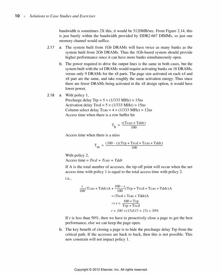
The new equations for policy 2,
Access time when we can hide precharge delay = Trcd + Tcas + Tddr
Access time when precharge delay is in the critical path = Trcd + Tcas + Trp + Tddr
Equation 1 will now become,
r = 90 × 15/30 = 45%
c. For any row buffer hit rate, policy 2 requires additional r × (2 + 4) nJ peraccess. If r = 50%, then policy 2 requires 3nJ of additional energy.
2.19 Hibernating will be useful when the static energy saved in DRAM is at least equalto the energy required to copy from DRAM to Flash and then back to DRAM.
DRAM dynamic energy to read/write is negligible compared to Flash and can beignored.
= 400 seconds
The factor 2 in the above equation is because to hibernate and wakeup, both Flashand DRAM have to be read and written once.
2.20 a. Yes. The application and production environment can be run on a VM hostedon a development machine.
b. Yes. Applications can be redeployed on the same environment on top of VMsrunning on different hardware. This is commonly called business continuity.
c. No. Depending on support in the architecture, virtualizing I/O may add sig-nificant or very significant performance overheads.
d. Yes. Applications running on different virtual machines are isolated fromeach other.
e. Yes. See “Devirtualizable virtual machines enabling general, single-node,online maintenance,” David Lowell, Yasushi Saito, and Eileen Samberg, inthe Proceedings of the 11th ASPLOS, 2004, pages 211–223.
2.21 a. Programs that do a lot of computation but have small memory working setsand do little I/O or other system calls.
b. The slowdown above was 60% for 10%, so 20% system time would run120% slower.
c. The median slowdown using pure virtualization is 10.3, while for para virtu-alization the median slowdown is 3.76.
r100--------- Tcas Tddr+( )A
100 r–100
----------------- Trp Trcd Tcas Tddr+ + +( )A+
0.9 Trcd Tcas Tddr+ +( )× A 0.1 Trcd Tcas Trp Tddr+ + +( )×+=
r⇒ 90Trp
Trp Trcd+----------------------------⎝ ⎠⎛ ⎞×=
Time8 10
92 2.56 10
6–××××64 1.6×
-------------------------------------------------------------=
Copyright © 2012 Elsevier, Inc. All rights reserved.
12 ■ Solutions to Case Studies and Exercises
d. The null call and null I/O call have the largest slowdown. These have no realwork to outweigh the virtualization overhead of changing protection levels,so they have the largest slowdowns.
2.22 The virtual machine running on top of another virtual machine would have to emu-late privilege levels as if it was running on a host without VT-x technology.
2.23 a. As of the date of the Computer paper, AMD-V adds more support for virtual-izing virtual memory, so it could provide higher performance for memory-intensive applications with large memory footprints.
b. Both provide support for interrupt virtualization, but AMD’s IOMMU alsoadds capabilities that allow secure virtual machine guest operating systemaccess to selected devices.
2.24 Open hands-on exercise, no fixed solution.
2.25 a. These results are from experiments on a 3.3GHz Intel® Xeon® ProcessorX5680 with Nehalem architecture (westmere at 32nm). The number of missesper 1K instructions of L1 Dcache increases significantly by more than 300Xwhen input data size goes from 8KB to 64 KB, and keeps relatively constantaround 300/1K instructions for all the larger data sets. Similar behavior withdifferent flattening points on L2 and L3 caches are observed.
b. The IPC decreases by 60%, 20%, and 66% when input data size goes from8KB to 128 KB, from 128KB to 4MB, and from 4MB to 32MB, respectively.This shows the importance of all caches. Among all three levels, L1 and L3caches are more important. This is because the L2 cache in the Intel® Xeon®Processor X5680 is relatively small and slow, with capacity being 256KB andlatency being around 11 cycles.
c. For a recent Intel i7 processor (3.3GHz Intel® Xeon® Processor X5680),when the data set size is increased from 8KB to 128KB, the number of L1Dcache misses per 1K instructions increases by around 300, and the numberof L2 cache misses per 1K instructions remains negligible. With a 11 cyclemiss penalty, this means that without prefetching or latency tolerance fromout-of-order issue we would expect there to be an extra 3300 cycles per 1Kinstructions due to L1 misses, which means an increase of 3.3 cycles perinstruction on average. The measured CPI with the 8KB input data size is1.37. Without any latency tolerance mechanisms we would expect the CPI ofthe 128KB case to be 1.37 + 3.3 = 4.67. However, the measured CPI of the128KB case is 3.44. This means that memory latency hiding techniques suchas OOO execution, prefetching, and non-blocking caches improve the perfor-mance by more than 26%.
Copyright © 2012 Elsevier, Inc. All rights reserved.

Chapter 3 Solutions ■ 13
Case Study 1: Exploring the Impact of Microarchitectural Techniques 2
3.1 The baseline performance (in cycles, per loop iteration) of the code sequence inFigure 3.48, if no new instruction’s execution could be initiated until the previ-ous instruction’s execution had completed, is 40. See Figure S.2. Each instruc-tion requires one clock cycle of execution (a clock cycle in which thatinstruction, and only that instruction, is occupying the execution units; sinceevery instruction must execute, the loop will take at least that many clockcycles). To that base number, we add the extra latency cycles. Don’t forget thebranch shadow cycle.
3.2 How many cycles would the loop body in the code sequence in Figure 3.48require if the pipeline detected true data dependencies and only stalled on those,rather than blindly stalling everything just because one functional unit is busy?The answer is 25, as shown in Figure S.3. Remember, the point of the extralatency cycles is to allow an instruction to complete whatever actions it needs, inorder to produce its correct output. Until that output is ready, no dependentinstructions can be executed. So the first LD must stall the next instruction forthree clock cycles. The MULTD produces a result for its successor, and thereforemust stall 4 more clocks, and so on.
Figure S.2 Baseline performance (in cycles, per loop iteration) of the code sequencein Figure 3.48.
Chapter 3 Solutions
Loop: LD F2,0(Rx) 1 + 4
DIVD F8,F2,F0 1 + 12
MULTD F2,F6,F2 1 + 5
LD F4,0(Ry) 1 + 4
ADDD F4,F0,F4 1 + 1
ADDD F10,F8,F2 1 + 1
ADDI Rx,Rx,#8 1
ADDI Ry,Ry,#8 1
SD F4,0(Ry) 1 + 1
SUB R20,R4,Rx 1
BNZ R20,Loop 1 + 1____
cycles per loop iter 40
Copyright © 2012 Elsevier, Inc. All rights reserved.

14 ■ Solutions to Case Studies and Exercises
3.3 Consider a multiple-issue design. Suppose you have two execution pipelines, eachcapable of beginning execution of one instruction per cycle, and enough fetch/decode bandwidth in the front end so that it will not stall your execution. Assumeresults can be immediately forwarded from one execution unit to another, or to itself.Further assume that the only reason an execution pipeline would stall is to observe atrue data dependency. Now how many cycles does the loop require? The answeris 22, as shown in Figure S.4. The LD goes first, as before, and the DIVD must waitfor it through 4 extra latency cycles. After the DIVD comes the MULTD, which can runin the second pipe along with the DIVD, since there’s no dependency between them.(Note that they both need the same input, F2, and they must both wait on F2’s readi-ness, but there is no constraint between them.) The LD following the MULTD does notdepend on the DIVD nor the MULTD, so had this been a superscalar-order-3 machine,
Figure S.3 Number of cycles required by the loop body in the code sequence inFigure 3.48.
Loop: LD
<stall>
<stall>
<stall>
<stall>
DIVD
MULTD
LD
<stall due to LD latency>
<stall due to LD latency>
<stall due to LD latency>
<stall due to LD latency>
ADDD
<stall due to ADDD latency>
<stall due to DIVD latency>
<stall due to DIVD latency>
<stall due to DIVD latency>
<stall due to DIVD latency>
ADDD
ADDI
ADDI
SD
SUB
BNZ
<stall branch delay slot>
cycles per loop iter
F2,0(Rx)
F8,F2,F0
F2,F6,F2
F4,0(Ry)
F4,F0,F4
F10,F8,F2
Rx,Rx,#8
Ry,Ry,#8
F4,0(Ry)
R20,R4,Rx
R20,Loop
1 + 4
1 + 12
1 + 5
1 + 4
1 + 1
1 + 1
1
1
1 + 1
1
1 + 1
------
25
Copyright © 2012 Elsevier, Inc. All rights reserved.

Chapter 3 Solutions ■ 15
that LD could conceivably have been executed concurrently with the DIVD and theMULTD. Since this problem posited a two-execution-pipe machine, the LD executes inthe cycle following the DIVD/MULTD. The loop overhead instructions at the loop’sbottom also exhibit some potential for concurrency because they do not depend onany long-latency instructions.
3.4 Possible answers:
1. If an interrupt occurs between N and N + 1, then N + 1 must not have beenallowed to write its results to any permanent architectural state. Alternatively,it might be permissible to delay the interrupt until N + 1 completes.
2. If N and N + 1 happen to target the same register or architectural state (say,memory), then allowing N to overwrite what N + 1 wrote would be wrong.
3. N might be a long floating-point op that eventually traps. N + 1 cannot beallowed to change arch state in case N is to be retried.
Execution pipe 0 Execution pipe 1
Loop: LD F2,0(Rx) ; <nop>
<stall for LD latency> ; <nop>
<stall for LD latency> ; <nop>
<stall for LD latency> ; <nop>
<stall for LD latency> ; <nop>
DIVD F8,F2,F0 ; MULTD F2,F6,F2
LD F4,0(Ry) ; <nop>
<stall for LD latency> ; <nop>
<stall for LD latency> ; <nop>
<stall for LD latency> ; <nop>
<stall for LD latency> ; <nop>
ADD F4,F0,F4 ; <nop>
<stall due to DIVD latency> ; <nop>
<stall due to DIVD latency> ; <nop>
<stall due to DIVD latency> ; <nop>
<stall due to DIVD latency> ; <nop>
<stall due to DIVD latency> ; <nop>
<stall due to DIVD latency> ; <nop>
ADDD F10,F8,F2 ; ADDI Rx,Rx,#8
ADDI Ry,Ry,#8 ; SD F4,0(Ry)
SUB R20,R4,Rx ; BNZ R20,Loop
<nop> ; <stall due to BNZ>
cycles per loop iter 22
Figure S.4 Number of cycles required per loop.
Copyright © 2012 Elsevier, Inc. All rights reserved.

16 ■ Solutions to Case Studies and Exercises
Long-latency ops are at highest risk of being passed by a subsequent op. TheDIVD instr will complete long after the LD F4,0(Ry), for example.
3.5 Figure S.5 demonstrates one possible way to reorder the instructions to improve theperformance of the code in Figure 3.48. The number of cycles that this reorderedcode takes is 20.
3.6 a. Fraction of all cycles, counting both pipes, wasted in the reordered codeshown in Figure S.5:
11 ops out of 2x20 opportunities.1 – 11/40 = 1 – 0.275 = 0.725
b. Results of hand-unrolling two iterations of the loop from code shown in Figure S.6:
c. Speedup =
Speedup = 20 / (22/2)Speedup = 1.82
Execution pipe 0 Execution pipe 1
Loop: LD F2,0(Rx) ; LD F4,0(Ry)
<stall for LD latency> ; <stall for LD latency>
<stall for LD latency> ; <stall for LD latency>
<stall for LD latency> ; <stall for LD latency>
<stall for LD latency> ; <stall for LD latency>
DIVD F8,F2,F0 ; ADDD F4,F0,F4
MULTD F2,F6,F2 ; <stall due to ADDD latency>
<stall due to DIVD latency> ; SD F4,0(Ry)
<stall due to DIVD latency> ; <nop> #ops: 11
<stall due to DIVD latency> ; <nop> #nops: (20 × 2) – 11 = 29
<stall due to DIVD latency> ; ADDI Rx,Rx,#8
<stall due to DIVD latency> ; ADDI Ry,Ry,#8
<stall due to DIVD latency> ; <nop>
<stall due to DIVD latency> ; <nop>
<stall due to DIVD latency> ; <nop>
<stall due to DIVD latency> ; <nop>
<stall due to DIVD latency> ; <nop>
<stall due to DIVD latency> ; SUB R20,R4,Rx
ADDD F10,F8,F2 ; BNZ R20,Loop
<nop> ; <stall due to BNZ>
cycles per loop iter 20
Figure S.5 Number of cycles taken by reordered code.
exec time w/o enhancementexec time with enhancement--------------------------------------------------------------------
Copyright © 2012 Elsevier, Inc. All rights reserved.
Chapter 3 Solutions ■ 17
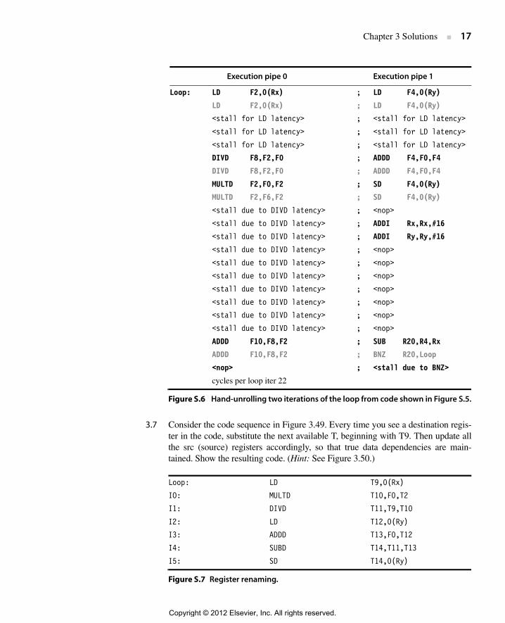
3.7 Consider the code sequence in Figure 3.49. Every time you see a destination regis-ter in the code, substitute the next available T, beginning with T9. Then update allthe src (source) registers accordingly, so that true data dependencies are main-tained. Show the resulting code. (Hint: See Figure 3.50.)
Execution pipe 0 Execution pipe 1
Loop: LD F2,0(Rx) ; LD F4,0(Ry)
LD F2,0(Rx) ; LD F4,0(Ry)
<stall for LD latency> ; <stall for LD latency>
<stall for LD latency> ; <stall for LD latency>
<stall for LD latency> ; <stall for LD latency>
DIVD F8,F2,F0 ; ADDD F4,F0,F4
DIVD F8,F2,F0 ; ADDD F4,F0,F4
MULTD F2,F0,F2 ; SD F4,0(Ry)
MULTD F2,F6,F2 ; SD F4,0(Ry)
<stall due to DIVD latency> ; <nop>
<stall due to DIVD latency> ; ADDI Rx,Rx,#16
<stall due to DIVD latency> ; ADDI Ry,Ry,#16
<stall due to DIVD latency> ; <nop>
<stall due to DIVD latency> ; <nop>
<stall due to DIVD latency> ; <nop>
<stall due to DIVD latency> ; <nop>
<stall due to DIVD latency> ; <nop>
<stall due to DIVD latency> ; <nop>
<stall due to DIVD latency> ; <nop>
ADDD F10,F8,F2 ; SUB R20,R4,Rx
ADDD F10,F8,F2 ; BNZ R20,Loop
<nop> ; <stall due to BNZ>
cycles per loop iter 22
Figure S.6 Hand-unrolling two iterations of the loop from code shown in Figure S.5.
Loop: LD T9,0(Rx)
IO: MULTD T10,F0,T2
I1: DIVD T11,T9,T10
I2: LD T12,0(Ry)
I3: ADDD T13,F0,T12
I4: SUBD T14,T11,T13
I5: SD T14,0(Ry)
Figure S.7 Register renaming.
Copyright © 2012 Elsevier, Inc. All rights reserved.
18 ■ Solutions to Case Studies and Exercises
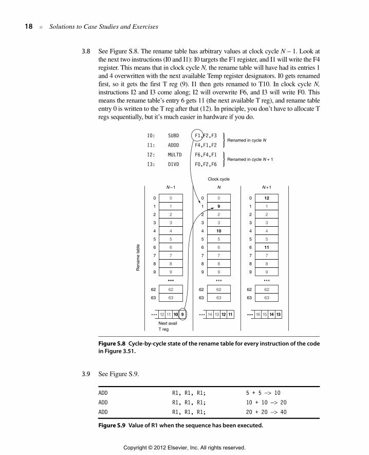
3.8 See Figure S.8. The rename table has arbitrary values at clock cycle N – 1. Look atthe next two instructions (I0 and I1): I0 targets the F1 register, and I1 will write the F4register. This means that in clock cycle N, the rename table will have had its entries 1and 4 overwritten with the next available Temp register designators. I0 gets renamedfirst, so it gets the first T reg (9). I1 then gets renamed to T10. In clock cycle N,instructions I2 and I3 come along; I2 will overwrite F6, and I3 will write F0. Thismeans the rename table’s entry 6 gets 11 (the next available T reg), and rename tableentry 0 is written to the T reg after that (12). In principle, you don’t have to allocate Tregs sequentially, but it’s much easier in hardware if you do.
3.9 See Figure S.9.
Figure S.8 Cycle-by-cycle state of the rename table for every instruction of the codein Figure 3.51.
ADD R1, R1, R1; 5 + 5 −> 10ADD R1, R1, R1; 10 + 10 −> 20ADD R1, R1, R1; 20 + 20 −> 40
Figure S.9 Value of R1 when the sequence has been executed.
Renamed in cycle N
Renamed in cycle N + 1
N +1NN –1
0
1
2
3
4
5
6
7
8
9
0
9
2
3
10
5
6
7
8
9
12
1
2
3
4
5
11
7
8
9
Clock cycle
I0:
I1:
I2:
I3:
SUBD
ADDD
MULTD
DIVD
F1,F2,F3
F4,F1,F2
F6,F4,F1
F0,F2,F6
Next availT reg
Ren
ame
tabl
e
62
63
0
1
2
3
4
5
6
7
8
9
62
63
12 11 10 9
62
63
0
1
2
3
4
5
6
7
8
9
62
63
62
63
0
1
2
3
4
5
6
7
8
9
62
63
14 13 12 11 16 15 14 13
Copyright © 2012 Elsevier, Inc. All rights reserved.
Chapter 3 Solutions ■ 19
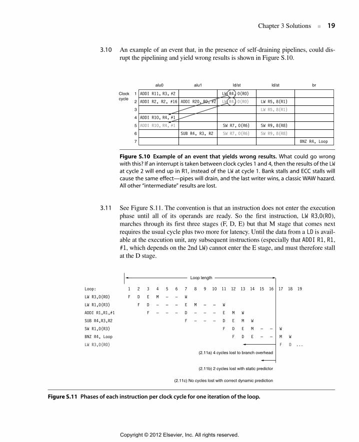
3.10 An example of an event that, in the presence of self-draining pipelines, could dis-rupt the pipelining and yield wrong results is shown in Figure S.10.
3.11 See Figure S.11. The convention is that an instruction does not enter the executionphase until all of its operands are ready. So the first instruction, LW R3,0(R0),marches through its first three stages (F, D, E) but that M stage that comes nextrequires the usual cycle plus two more for latency. Until the data from a LD is avail-able at the execution unit, any subsequent instructions (especially that ADDI R1, R1,#1, which depends on the 2nd LW) cannot enter the E stage, and must therefore stallat the D stage.
Figure S.10 Example of an event that yields wrong results. What could go wrongwith this? If an interrupt is taken between clock cycles 1 and 4, then the results of the LWat cycle 2 will end up in R1, instead of the LW at cycle 1. Bank stalls and ECC stalls willcause the same effect—pipes will drain, and the last writer wins, a classic WAW hazard.All other “intermediate” results are lost.
Figure S.11 Phases of each instruction per clock cycle for one iteration of the loop.
alu0
ADDI R10, R4, #1
ADDI R10, R4, #1
ADDI R11, R3, #2
ADDI R2, R2, #16
1
2
3
4
5
6
7
Clock cycle
alu1
ADDI R20, R0, #2
SUB R4, R3, R2
ld/st
LW R4, 0(R0)
LW R4, 0(R0) LW R5, 8(R1)
LW R5, 8(R1)
SW R9, 8(R8)
BNZ R4, Loop
SW R9, 8(R8)
SW R7, 0(R6)
SW R7, 0(R6)
ld/st br
Loop length
Loop:
LW R3,0(R0)
LW R1,0(R3)
ADDI R1,R1,#1
SUB R4,R3,R2
SW R1,0(R3)
BNZ R4, Loop
LW R3,0(R0)
(2.11a) 4 cycles lost to branch overhead
(2.11b) 2 cycles lost with static predictor
(2.11c) No cycles lost with correct dynamic prediction
1
F
2
D
F
3
E
D
F
4
M
–
–
5
–
–
–
6
–
–
–
7
W
E
D
F
8
M
–
–
9
–
–
–
10
–
–
–
11
W
E
D
F
12
M
E
D
F
13
W
M
E
D
14
W
M
E
15
–
–
16
–
–
17
W
M
F
18
W
D
19
...
Copyright © 2012 Elsevier, Inc. All rights reserved.

20 ■ Solutions to Case Studies and Exercises
a. 4 cycles lost to branch overhead. Without bypassing, the results of the SUBinstruction are not available until the SUB’s W stage. That tacks on an extra 4clock cycles at the end of the loop, because the next loop’s LW R1 can’t beginuntil the branch has completed.
b. 2 cycles lost w/ static predictor. A static branch predictor may have a heuristiclike “if branch target is a negative offset, assume it’s a loop edge, and loopsare usually taken branches.” But we still had to fetch and decode the branchto see that, so we still lose 2 clock cycles here.
c. No cycles lost w/ correct dynamic prediction. A dynamic branch predictorremembers that when the branch instruction was fetched in the past, it eventu-ally turned out to be a branch, and this branch was taken. So a “predicted taken”will occur in the same cycle as the branch is fetched, and the next fetch afterthat will be to the presumed target. If correct, we’ve saved all of the latencycycles seen in 3.11 (a) and 3.11 (b). If not, we have some cleaning up to do.
3.12 a. See Figure S.12.
Figure S.12 Instructions in code where register renaming improves performance.
LD
DIVD
MULTD
LD
ADDD
ADDD
ADDI
ADDI
SD
SUB
BNZ
F2,0(Rx)
F8,F2,F0
F2,F8,F2
F4,0(Ry)
F4,F0,F4
F10,F8,F2
Rx,Rx,#8
Ry,Ry,#8
F4,0(Ry)
R20,R4,Rx
R20,Loop
; reg renaming doesn’t really help here, due to
; true data dependencies on F8 and F2
; this LD is independent of the previous 3
; instrs and can be performed earlier than
; pgm order. It feeds the next ADDD, and ADDD
; feeds the SD below. But there’s a true data
; dependency chain through all, so no benefit
; This ADDD still has to wait for DIVD latency,
; no matter what you call their rendezvous reg
; rename for next loop iteration
; rename for next loop iteration
; This SD can start when the ADDD’s latency has
; transpired. With reg renaming, doesn’t have
; to wait until the LD of (a different) F4 has
; completed.
Copyright © 2012 Elsevier, Inc. All rights reserved.

Chapter 3 Solutions ■ 21
b. See Figure S.13. The number of clock cycles taken by the code sequence is 25.
c. See Figures S.14 and S.15. The bold instructions are those instructions thatare present in the RS, and ready for dispatch. Think of this exercise from theReservation Station’s point of view: at any given clock cycle, it can only“see” the instructions that were previously written into it, that have notalready dispatched. From that pool, the RS’s job is to identify and dispatchthe two eligible instructions that will most boost machine performance.
Figure S.13 Number of clock cycles taken by the code sequence.
Figure S.14 Candidates for dispatch.
alu0
ADDI Rx,Rx,#8
SUB R20,R4,Rx
MULTD F2,F8,F2
DIVD F8,F2,F0
BNZ R20,Loop
Branch shadow
ADDI Ry,Ry,#8
ADDD F4,F0,F4
ADDD F10,F8,F2
1
2
3
4
5
6
7
8
. . .
18
19
20
21
22
23
24
25
Clock cycle
Note: these ADDI’s aregenerating Rx,y for nextloop iteration, not this one.
Cycle op was dispatched to FU
alu1 ld/st
LD F2,0(Rx)
LD F4,0(Ry)
SD F4,0(Ry)
LD latency
ADDD latencyD
IVD
latency
MULTD latency
LD
DIVD
MULTD
LD
ADDD
ADDD
ADDI
ADDI
SD
SUB
BNZ
10
F2, 0(Rx)
F8,F2,F0
F2,F8,F2
F4, 0(Ry)
F4,F0,F4
F10,F8,F2
Rx,Rx,#8
Ry,Ry,#8
F4,0(Ry)
R20,R4,Rx
20,Loop
LD
DIVD
MULTD
LD
ADDD
ADDD
ADDI
ADDI
SD
SUB
BNZ
2
F2, 0(Rx)
F8,F2,F0
F2,F8,F2
F4, 0(Ry)
F4,F0,F4
F10,F8,F2
Rx,Rx,#8
Ry,Ry,#8
F4,0(Ry)
R20,R4,Rx
20,Loop
LD
DIVD
MULTD
LD
ADDD
ADDD
ADDI
ADDI
SD
SUB
BNZ
3
F2, 0(Rx)
F8,F2,F0
F2,F8,F2
F4, 0(Ry)
F4,F0,F4
F10,F8,F2
Rx,Rx,#8
Ry,Ry,#8
F4,0(Ry)
R20,R4,Rx
20,Loop
LD
DIVD
MULTD
LD
ADDD
ADDD
ADDI
ADDI
SD
SUB
BNZ
4
F2, 0(Rx)
F8,F2,F0
F2,F8,F2
F4, 0(Ry)
F4,F0,F4
F10,F8,F2
Rx,Rx,#8
Ry,Ry,#8
F4,0(Ry)
R20,R4,Rx
20,Loop
LD
DIVD
MULTD
LD
ADDD
ADDD
ADDI
ADDI
SD
SUB
BNZ
5 6
F2, 0(Rx)
F8,F2,F0
F2,F8,F2
F4, 0(Ry)
F4,F0,F4
F10,F8,F2
Rx,Rx,#8
Ry,Ry,#8
F4,0(Ry)
R20,R4,Rx
20,Loop
LD
DIVD
MULTD
LD
ADDD
ADDD
ADDI
ADDI
SD
SUB
BNZ
F2, 0(Rx)
F8,F2,F0
F2,F8,F2
F4, 0(Ry)
F4,F0,F4
F10,F8,F2
Rx,Rx,#8
Ry,Ry,#8
F4,0(Ry)
R20,R4,Rx
20,Loop
Candidates for dispatch in boldFirst 2 instructions appear in RS
Copyright © 2012 Elsevier, Inc. All rights reserved.
22 ■ Solutions to Case Studies and Exercises
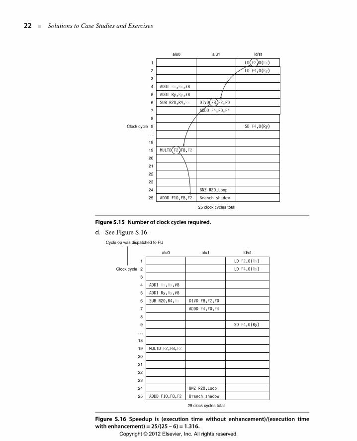
d. See Figure S.16.
Figure S.15 Number of clock cycles required.
Figure S.16 Speedup is (execution time without enhancement)/(execution timewith enhancement) = 25/(25 – 6) = 1.316.
alu0
ADDI Rx,Rx,#8
SUB R20,R4,Rx
MULTD F2,F8,F2
BNZ R20,Loop
Branch shadow
ADDI Ry,Ry,#8
ADDD F4,F0,F4
DIVD F8,F2,F0
ADDD F10,F8,F2
1
2
3
4
5
6
7
8
9
. . .
18
19
20
21
22
23
24
25
Clock cycle
25 clock cycles total
alu1 ld/st
LD F2,0(Rx)
LD F4,0(Ry)
SD F4,0(Ry)
alu0
ADDI Rx,Rx,#8
SUB R20,R4,Rx
MULTD F2,F8,F2
BNZ R20,Loop
Branch shadow
ADDI Ry,Ry,#8
ADDD F4,F0,F4
DIVD F8,F2,F0
ADDD F10,F8,F2
1
2
3
4
5
6
7
8
9
. . .
18
19
20
21
22
23
24
25
Clock cycle
25 clock cycles total
alu1 ld/st
LD F2,0(Rx)
LD F4,0(Ry)
SD F4,0(Ry)
Cycle op was dispatched to FU
Copyright © 2012 Elsevier, Inc. All rights reserved.
Chapter 3 Solutions ■ 23
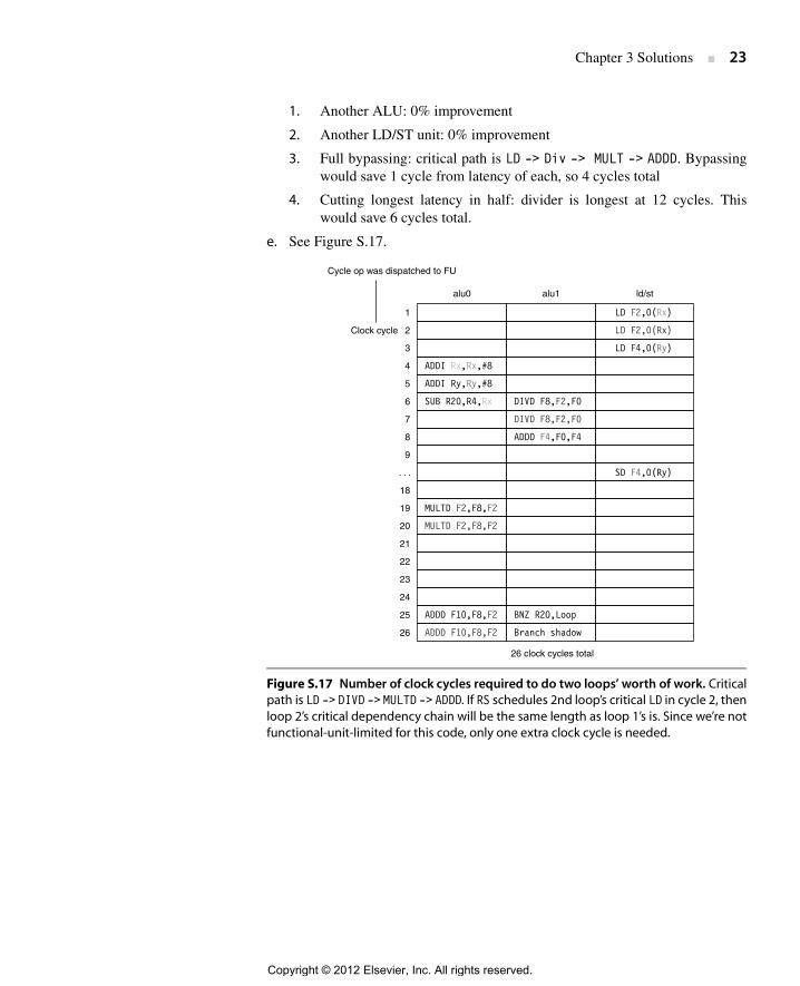
1. Another ALU: 0% improvement
2. Another LD/ST unit: 0% improvement
3. Full bypassing: critical path is LD -> Div -> MULT -> ADDD. Bypassingwould save 1 cycle from latency of each, so 4 cycles total
4. Cutting longest latency in half: divider is longest at 12 cycles. Thiswould save 6 cycles total.
e. See Figure S.17.
Figure S.17 Number of clock cycles required to do two loops’ worth of work. Criticalpath is LD -> DIVD -> MULTD -> ADDD. If RS schedules 2nd loop’s critical LD in cycle 2, thenloop 2’s critical dependency chain will be the same length as loop 1’s is. Since we’re notfunctional-unit-limited for this code, only one extra clock cycle is needed.
alu0
ADDI Rx,Rx,#8
SUB R20,R4,Rx
MULTD F2,F8,F2
BNZ R20,Loop
Branch shadow
ADDI Ry,Ry,#8
DIVD F8,F2,F0
ADDD F4,F0,F4
DIVD F8,F2,F0
ADDD F10,F8,F2
MULTD F2,F8,F2
ADDD F10,F8,F2
1
2
3
4
5
6
7
8
9
. . .
18
19
20
21
22
23
24
25
26
Clock cycle
26 clock cycles total
alu1 ld/st
LD F2,0(Rx)
LD F2,0(Rx)
LD F4,0(Ry)
SD F4,0(Ry)
Cycle op was dispatched to FU
Copyright © 2012 Elsevier, Inc. All rights reserved.
24 ■ Solutions to Case Studies and Exercises
Exercises
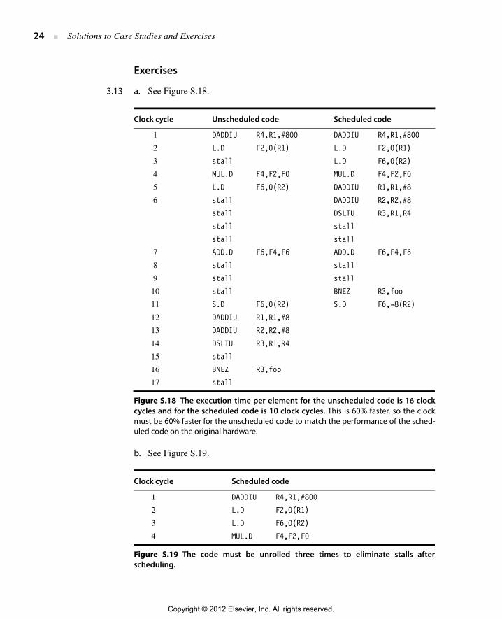
3.13 a. See Figure S.18.
b. See Figure S.19.
Clock cycle Unscheduled code Scheduled code
1 DADDIU R4,R1,#800 DADDIU R4,R1,#800
2 L.D F2,0(R1) L.D F2,0(R1)
3 stall L.D F6,0(R2)
4 MUL.D F4,F2,F0 MUL.D F4,F2,F0
5 L.D F6,0(R2) DADDIU R1,R1,#8
6 stall DADDIU R2,R2,#8
stall DSLTU R3,R1,R4
stall stall
stall stall
7 ADD.D F6,F4,F6 ADD.D F6,F4,F6
8 stall stall
9 stall stall
10 stall BNEZ R3,foo
11 S.D F6,0(R2) S.D F6,-8(R2)
12 DADDIU R1,R1,#8
13 DADDIU R2,R2,#8
14 DSLTU R3,R1,R4
15 stall
16 BNEZ R3,foo
17 stall
Figure S.18 The execution time per element for the unscheduled code is 16 clockcycles and for the scheduled code is 10 clock cycles. This is 60% faster, so the clockmust be 60% faster for the unscheduled code to match the performance of the sched-uled code on the original hardware.
Clock cycle Scheduled code
1 DADDIU R4,R1,#800
2 L.D F2,0(R1)
3 L.D F6,0(R2)
4 MUL.D F4,F2,F0
Figure S.19 The code must be unrolled three times to eliminate stalls afterscheduling.
Copyright © 2012 Elsevier, Inc. All rights reserved.

Chapter 3 Solutions ■ 25
c. See Figures S.20 and S.21.
Unrolled 6 times:
5 L.D F2,8(R1)
6 L.D F10,8(R2)
7 MUL.D F8,F2,F0
8 L.D F2,8(R1)
9 L.D F14,8(R2)
10 MUL.D F12,F2,F0
11 ADD.D F6,F4,F6
12 DADDIU R1,R1,#24
13 ADD.D F10,F8,F10
14 DADDIU R2,R2,#24
15 DSLTU R3,R1,R4
16 ADD.D F14,F12,F14
17 S.D F6,-24(R2)
18 S.D F10,-16(R2)
19 BNEZ R3,foo
20 S.D F14,-8(R2)
Figure S.19 Continued
CycleMemory reference 1
Memory reference 2 FP operation 1 FP operation 2
Integer opera-tion/branch
1 L.D F1,0(R1) L.D F2,8(R1)
2 L.D F3,16(R1) L.D F4,24(R1)
3 L.D F5,32(R1) L.D F6,40(R1) MUL.D F1,F1,F0 MUL.D F2,F2,F0
4 L.D F7,0(R2) L.D F8,8(R2) MUL.D F3,F3,F0 MUL.D F4,F4,F0
5 L.D F9,16(R2) L.D F10,24(R2) MUL.D F5,F5,F0 MUL.D F6,F6,F0
6 L.D F11,32(R2) L.D F12,40(R2)
7 DADDIU R1,R1,48
8 DADDIU R2,R2,48
Figure S.20 15 cycles for 34 operations, yielding 2.67 issues per clock, with a VLIW efficiency of 34 operationsfor 75 slots = 45.3%. This schedule requires 12 floating-point registers.
Copyright © 2012 Elsevier, Inc. All rights reserved.

26 ■ Solutions to Case Studies and Exercises
Unrolled 10 times:
9 ADD.D F7,F7,F1 ADD.D F8,F8,F2
10 ADD.D F9,F9,F3 ADD.D F10,F10,F4
11 ADD.D F11,F11,F5 ADD.D F12,F12,F6
12 DSLTUR3,R1,R4
13 S.D F7,-48(R2) S.D F8,-40(R2)
14 S.D F9,-32(R2) S.D F10,-24(R2)
15 S.D F11,-16(R2) S.D F12,-8(R2) BNEZ R3,foo
Figure S.20 Continued
CycleMemory reference 1
Memory reference 2 FP operation 1 FP operation 2
Integer operation/branch
1 L.D F1,0(R1) L.D F2,8(R1)
2 L.D F3,16(R1) L.D F4,24(R1)
3 L.D F5,32(R1) L.D F6,40(R1) MUL.D F1,F1,F0 MUL.D F2,F2,F0
4 L.D F7,48(R1) L.D F8,56(R1) MUL.D F3,F3,F0 MUL.D F4,F4,F0
5 L.D F9,64(R1) L.D F10,72(R1) MUL.D F5,F5,F0 MUL.D F6,F6,F0
6 L.D F11,0(R2) L.D F12,8(R2) MUL.D F7,F7,F0 MUL.D F8,F8,F0
7 L.D F13,16(R2) L.D F14,24(R2) MUL.D F9,F9,F0 MUL.D F10,F10,F0 DADDIU R1,R1,48
8 L.D F15,32(R2) L.D F16,40(R2) DADDIU R2,R2,48
9 L.D F17,48(R2) L.D F18,56(R2) ADD.D F11,F11,F1 ADD.D F12,F12,F2
10 L.D F19,64(R2) L.D F20,72(R2) ADD.D F13,F13,F3 ADD.D F14,F14,F4
11 ADD.D F15,F15,F5 ADD.D F16,F16,F6
12 ADD.D F17,F17,F7 ADD.D F18,F18,F8 DSLTU R3,R1,R4
13 S.D F11,-80(R2) S.D F12,-72(R2) ADD.D F19,F19,F9 ADD.D F20,F20,F10
14 S.D F13,-64(R2) S.D F14,-56(R2)
15 S.D F15,-48(R2) S.D F16,-40(R2)
16 S.D F17,-32(R2) S.D F18,-24(R2)
17 S.D F19,-16(R2) S.D F20,-8(R2) BNEZ R3,foo
Figure S.21 17 cycles for 54 operations, yielding 3.18 issues per clock, with a VLIW efficiency of 54 operations for85 slots = 63.5%. This schedule requires 20 floating-point registers.
Copyright © 2012 Elsevier, Inc. All rights reserved.

Chapter 3 Solutions ■ 27
3.14 a. See Figure S.22.
Iteration Instruction Issues atExecutes/Memory Write CDB at Comment
1 L.D F2,0(R1) 1 2 3 First issue
1 MUL.D F4,F2,F0 2 4 19 Wait for F2Mult rs [3–4]Mult use [5–18]
1 L.D F6,0(R2) 3 4 5 Ldbuf [4]
1 ADD.D F6,F4,F6 4 20 30 Wait for F4Add rs [5–20]Add use [21–29]
1 S.D F6,0(R2) 5 31 Wait for F6Stbuf1 [6–31]
1 DADDIU R1,R1,#8 6 7 8
1 DADDIU R2,R2,#8 7 8 9
1 DSLTU R3,R1,R4 8 9 10
1 BNEZ R3,foo 9 11 Wait for R3
2 L.D F2,0(R1) 10 12 13 Wait for BNEZLdbuf [11–12]
2 MUL.D F4,F2,F0 11 1419
34 Wait for F2Mult busyMult rs [12–19]Mult use [20–33]
2 L.D F6,0(R2) 12 13 14 Ldbuf [13]
2 ADD.D F6,F4,F6 13 35 45 Wait for F4Add rs [14–35]Add use [36–44]
2 S.D F6,0(R2) 14 46 Wait for F6Stbuf [15–46]
2 DADDIU R1,R1,#8 15 16 17
2 DADDIU R2,R2,#8 16 17 18
2 DSLTU R3,R1,R4 17 18 20
2 BNEZ R3,foo 18 20 Wait for R3
3 L.D F2,0(R1) 19 21 22 Wait for BNEZLdbuf [20–21]
3 MUL.D F4,F2,F0 20 2334
49 Wait for F2Mult busyMult rs [21–34]Mult use [35–48]
3 L.D F6,0(R2) 21 22 23 Ldbuf [22]
3 ADD.D F6,F4,F6 22 50 60 Wait for F4Add rs [23–49]Add use [51–59]
Figure S.22 Solution for exercise 3.14a.
Copyright © 2012 Elsevier, Inc. All rights reserved.

28 ■ Solutions to Case Studies and Exercises
b. See Figure S.23.
3 S.D F6,0(R2) 23 55 Wait for F6Stbuf [24–55]
3 DADDIU R1,R1,#8 24 25 26
3 DADDIU R2,R2,#8 25 26 27
3 DSLTU R3,R1,R4 26 27 28
3 BNEZ R3,foo 27 29 Wait for R3
Figure S.22 Continued
Iteration Instruction Issues atExecutes/Memory Write CDB at Comment
1 L.D F2,0(R1) 1 2 3
1 MUL.D F4,F2,F0 1 4 19 Wait for F2Mult rs [2–4]Mult use [5]
1 L.D F6,0(R2) 2 3 4 Ldbuf [3]
1 ADD.D F6,F4,F6 2 20 30 Wait for F4Add rs [3–20]Add use [21]
1 S.D F6,0(R2) 3 31 Wait for F6Stbuf [4–31]
1 DADDIU R1,R1,#8 3 4 5
1 DADDIU R2,R2,#8 4 5 6
1 DSLTU R3,R1,R4 4 6 7 INT busyINT rs [5–6]
1 BNEZ R3,foo 5 7 INT busyINT rs [6–7]
2 L.D F2,0(R1) 6 8 9 Wait for BEQZ
2 MUL.D F4,F2,F0 6 10 25 Wait for F2Mult rs [7–10]Mult use [11]
2 L.D F6,0(R2) 7 9 10 INT busyINT rs [8–9]
2 ADD.D F6,F4,F6 7 26 36 Wait for F4Add RS [8–26]Add use [27]
2 S.D F6,0(R2) 8 37 Wait for F6
2 DADDIU R1,R1,#8 8 10 11 INT busyINT rs [8–10]
Figure S.23 Solution for exercise 3.14b.
Copyright © 2012 Elsevier, Inc. All rights reserved.

Chapter 3 Solutions ■ 29
3.15 See Figure S.24.
2 DADDIU R2,R2,#8 9 11 12 INT busyINT rs [10–11]
2 DSLTU R3,R1,R4 9 12 13 INT busyINT rs [10–12]
2 BNEZ R3,foo 10 14 Wait for R3
3 L.D F2,0(R1) 11 15 16 Wait for BNEZ
3 MUL.D F4,F2,F0 11 17 32 Wait for F2Mult rs [12–17]Mult use [17]
3 L.D F6,0(R2) 12 16 17 INT busyINT rs [13–16]
3 ADD.D F6,F4,F6 12 33 43 Wait for F4Add rs [13–33]Add use [33]
3 S.D F6,0(R2) 14 44 Wait for F6INT rs full in 15
3 DADDIU R1,R1,#8 15 17 INT rs full and busyINT rs [17]
3 DADDIU R2,R2,#8 16 18 INT rs full and busyINT rs [18]
3 DSLTU R3,R1,R4 20 21 INT rs full
3 BNEZ R3,foo 21 22 INT rs full
Figure S.23 Continued
Instruction Issues at Executes/Memory Write CDB at
ADD.D F2,F4,F6 1 2 12
ADD R1,R1,R2 2 3 4
ADD R1,R1,R2 3 5 6
ADD R1,R1,R2 4 7 8
ADD R1,R1,R2 5 9 10
ADD R1,R1,R2 6 11 12 (CDB conflict)
Figure S.24 Solution for exercise 3.15.
Copyright © 2012 Elsevier, Inc. All rights reserved.
30 ■ Solutions to Case Studies and Exercises
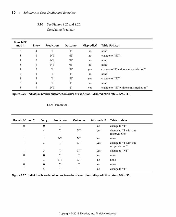
3.16 See Figures S.25 and S.26.
Correlating Predictor
Local Predictor
Branch PC mod 4 Entry Prediction Outcome Mispredict? Table Update
2 4 T T no none
3 6 NT NT no change to “NT”
1 2 NT NT no none
3 7 NT NT no none
1 3 T NT yes change to “T with one misprediction”
2 4 T T no none
1 3 T NT yes change to “NT”
2 4 T T no none
3 7 NT T yes change to “NT with one misprediction”
Figure S.25 Individual branch outcomes, in order of execution. Misprediction rate = 3/9 = .33.
Branch PC mod 2 Entry Prediction Outcome Mispredict? Table Update
0 0 T T no change to “T”
1 4 T NT yes change to “T with one misprediction”
1 1 NT NT no none
1 3 T NT yes change to “T with one misprediction”
1 3 T NT yes change to “NT”
0 0 T T no none
1 3 NT NT no none
0 0 T T no none
1 5 T T no change to “T”
Figure S.26 Individual branch outcomes, in order of execution. Misprediction rate = 3/9 = .33.
Copyright © 2012 Elsevier, Inc. All rights reserved.
Chapter 3 Solutions ■ 31
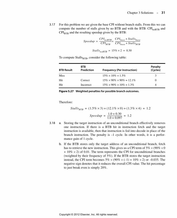
3.17 For this problem we are given the base CPI without branch stalls. From this we cancompute the number of stalls given by no BTB and with the BTB: CPInoBTB andCPIBTB and the resulting speedup given by the BTB:
To compute StallsBTB, consider the following table:
Therefore:
3.18 a. Storing the target instruction of an unconditional branch effectively removesone instruction. If there is a BTB hit in instruction fetch and the targetinstruction is available, then that instruction is fed into decode in place of thebranch instruction. The penalty is –1 cycle. In other words, it is a perfor-mance gain of 1 cycle.
b. If the BTB stores only the target address of an unconditional branch, fetchhas to retrieve the new instruction. This gives us a CPI term of 5% × (90% × 0+ 10% × 2) of 0.01. The term represents the CPI for unconditional branches(weighted by their frequency of 5%). If the BTB stores the target instructioninstead, the CPI term becomes 5% × (90% × (–1) + 10% × 2) or –0.035. Thenegative sign denotes that it reduces the overall CPI value. The hit percentageto just break even is simply 20%.
BTB ResultBTB Prediction Frequency (Per Instruction)
Penalty (Cycles)
Miss 15% × 10% = 1.5% 3
Hit Correct 15% × 90% × 90% = 12.1% 0
Hit Incorrect 15% × 90% × 10% = 1.3% 4
Figure S.27 Weighted penalties for possible branch outcomes.
SpeedupCPInoBTB
CPIBTB-------------------------
CPIbase Stallsbase+
CPIbase StallsBTB+---------------------------------------------------==
StallsnoBTB 15% 2× 0.30= =
StallsBTB 1.5% 3×( ) 12.1% 0×( ) 1.3% 4×( )+ + 1.2
Speedup1.0 0.30+1.0 0.097+--------------------------- 1.2
= =
= =
Copyright © 2012 Elsevier, Inc. All rights reserved.

32 ■ Solutions to Case Studies and Exercises
Case Study: Implementing a Vector Kernel on a Vector Processor and GPU
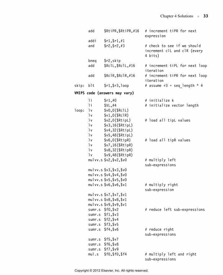
4.1 MIPS code (answers may vary)
li $r1,#0 # initialize kloop: l.s $f0,0($RtipL) # load all values for first
expressionl.s $f1,0($RclL)l.s $f2,4($RtipL)l.s $f3,4($RclL)l.s $f4,8($RtipL)l.s $f5,8($RclL)l.s $f6,12($RtipL)l.s $f7,12($RclL)l.s $f8,0($RtipR)l.s $f9,0($RclR)l.s $f10,4($RtipR)l.s $f11,4($RclR)l.s $f12,8($RtipR)l.s $f13,8($RclR)l.s $f14,12($RtipR)l.s $f15,12($RclR)mul.s $f16,$f0,$f1 # first four multipliesmul.s $f17,$f2,$f3mul.s $f18,$f4,$f5mul.s $f19,$f6,$f7add.s $f20,$f16,$f17 # accumulateadd.s $f20,$f20,$f18add.s $f20,$f20,$f19mul.s $f16,$f8,$f9 # second four multipliesmul.s $f17,$f10,$f11mul.s $f18,$f12,$f13mul.s $f19,$f14,$f15add.s $f21,$f16,$f17 # accumulateadd.s $f21,$f21,$f18add.s $f21,$f21,$f19mul.s $f20,$f20,$f21 # final multiplyst.s $f20,0($RclP) # store resultadd $RclP,$RclP,#4 # increment clP for next
expressionadd $RtiPL,$RtiPL,#16 # increment tiPL for next
expression
Chapter 4 Solutions
Copyright © 2012 Elsevier, Inc. All rights reserved.
Chapter 4 Solutions ■ 33
add $RtiPR,$RtiPR,#16 # increment tiPR for next expression
addi $r1,$r1,#1and $r2,$r2,#3 # check to see if we should
increment clL and clR (every4 bits)
bneq $r2,skipadd $RclL,$RclL,#16 # increment tiPL for next loop
iterationadd $RclR,$RclR,#16 # increment tiPR for next loop
iterationskip: blt $r1,$r3,loop # assume r3 = seq_length * 4
VMIPS code (answers may vary)
li $r1,#0 # initialize kli $VL,#4 # initialize vector length
loop: lv $v0,0($RclL)lv $v1,0($RclR)lv $v2,0($RtipL) # load all tipL valueslv $v3,16($RtipL)lv $v4,32($RtipL)lv $v5,48($RtipL)lv $v6,0($RtipR) # load all tipR valueslv $v7,16($RtipR)lv $v8,32($RtipR)lv $v9,48($RtipR)mulvv.s $v2,$v2,$v0 # multiply left
sub-expressionsmulvv.s $v3,$v3,$v0mulvv.s $v4,$v4,$v0mulvv.s $v5,$v5,$v0mulvv.s $v6,$v6,$v1 # multiply right
sub-expressionmulvv.s $v7,$v7,$v1mulvv.s $v8,$v8,$v1mulvv.s $v9,$v9,$v1sumr.s $f0,$v2 # reduce left sub-expressionssumr.s $f1,$v3sumr.s $f2,$v4sumr.s $f3,$v5sumr.s $f4,$v6 # reduce right
sub-expressionssumr.s $f5,$v7sumr.s $f6,$v8sumr.s $f7,$v9mul.s $f0,$f0,$f4 # multiply left and right
sub-expressions
Copyright © 2012 Elsevier, Inc. All rights reserved.

34 ■ Solutions to Case Studies and Exercises
mul.s $f1,$f1,$f5mul.s $f2,$f2,$f6mul.s $f3,$f3,$f7s.s $f0,0($Rclp) # store resultss.s $f1,4($Rclp)s.s $f2,8($Rclp)s.s $f3,12($Rclp)add $RtiPL,$RtiPL,#64 # increment tiPL for next
expressionadd $RtiPR,$RtiPR,#64 # increment tiPR for next
expressionadd $RclP,$RclP,#16 # increment clP for next
expressionadd $RclL,$RclL,#16 # increment clL for next
expressionadd $RclR,$RclR,#16 # increment clR for next
expressionaddi $r1,$r1,#1blt $r1,$r3,loop # assume r3 = seq_length
4.2 MIPS: loop is 41 instructions, will iterate 500 × 4 = 2000 times, so roughly 82000instructionsVMIPS: loop is also 41 instructions but will iterate only 500 times, so roughly20500 instructions
4.3 1. lv # clL2. lv # clR3. lv mulvv.s # tiPL 04. lv mulvv.s # tiPL 15. lv mulvv.s # tiPL 26. lv mulvv.s # tiPL 37. lv mulvv.s # tiPR 08. lv mulvv.s # tiPR 19. lv mulvv.s # tiPR 210. lv mulvv.s # tiPR 311. sumr.s12. sumr.s13. sumr.s14. sumr.s15. sumr.s16. sumr.s17. sumr.s18. sumr.s
18 chimes, 4 results, 15 FLOPS per result, 18/15 = 1.2 cycles per FLOP
Copyright © 2012 Elsevier, Inc. All rights reserved.
Chapter 4 Solutions ■ 35
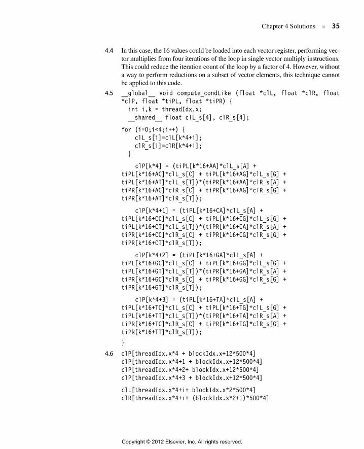
4.4 In this case, the 16 values could be loaded into each vector register, performing vec-tor multiplies from four iterations of the loop in single vector multiply instructions.This could reduce the iteration count of the loop by a factor of 4. However, withouta way to perform reductions on a subset of vector elements, this technique cannotbe applied to this code.
4.5 __global__ void compute_condLike (float *clL, float *clR, float*clP, float *tiPL, float *tiPR) { int i,k = threadIdx.x; __shared__ float clL_s[4], clR_s[4];
for (i=0;i<4;i++) { clL_s[i]=clL[k*4+i]; clR_s[i]=clR[k*4+i]; }
clP[k*4] = (tiPL[k*16+AA]*clL_s[A] + tiPL[k*16+AC]*clL_s[C] + tiPL[k*16+AG]*clL_s[G] + tiPL[k*16+AT]*clL_s[T])*(tiPR[k*16+AA]*clR_s[A] + tiPR[k*16+AC]*clR_s[C] + tiPR[k*16+AG]*clR_s[G] + tiPR[k*16+AT]*clR_s[T]);
clP[k*4+1] = (tiPL[k*16+CA]*clL_s[A] + tiPL[k*16+CC]*clL_s[C] + tiPL[k*16+CG]*clL_s[G] + tiPL[k*16+CT]*clL_s[T])*(tiPR[k*16+CA]*clR_s[A] + tiPR[k*16+CC]*clR_s[C] + tiPR[k*16+CG]*clR_s[G] + tiPR[k*16+CT]*clR_s[T]);
clP[k*4+2] = (tiPL[k*16+GA]*clL_s[A] + tiPL[k*16+GC]*clL_s[C] + tiPL[k*16+GG]*clL_s[G] + tiPL[k*16+GT]*clL_s[T])*(tiPR[k*16+GA]*clR_s[A] + tiPR[k*16+GC]*clR_s[C] + tiPR[k*16+GG]*clR_s[G] + tiPR[k*16+GT]*clR_s[T]);
clP[k*4+3] = (tiPL[k*16+TA]*clL_s[A] + tiPL[k*16+TC]*clL_s[C] + tiPL[k*16+TG]*clL_s[G] + tiPL[k*16+TT]*clL_s[T])*(tiPR[k*16+TA]*clR_s[A] + tiPR[k*16+TC]*clR_s[C] + tiPR[k*16+TG]*clR_s[G] + tiPR[k*16+TT]*clR_s[T]);
}
4.6 clP[threadIdx.x*4 + blockIdx.x+12*500*4]clP[threadIdx.x*4+1 + blockIdx.x+12*500*4]clP[threadIdx.x*4+2+ blockIdx.x+12*500*4]clP[threadIdx.x*4+3 + blockIdx.x+12*500*4]
clL[threadIdx.x*4+i+ blockIdx.x*2*500*4]clR[threadIdx.x*4+i+ (blockIdx.x*2+1)*500*4]
Copyright © 2012 Elsevier, Inc. All rights reserved.

36 ■ Solutions to Case Studies and Exercises
tipL[threadIdx.x*16+AA + blockIdx.x*2*500*16]tipL[threadIdx.x*16+AC + blockIdx.x*2*500*16]…
tipL[threadIdx.x*16+TT + blockIdx.x*2*500*16]
tipR[threadIdx.x*16+AA + (blockIdx.x*2+1)*500*16]tipR[threadIdx.x*16+AC +1 + (blockIdx.x*2+1)*500*16]…
tipR[threadIdx.x*16+TT +15+ (blockIdx.x*2+1)*500*16]
4.7
# compute address of clLmul.u64 %r1, %ctaid.x, 4000 # multiply block index by 4000mul.u64 %r2, %tid.x, 4 # multiply thread index by 4add.u64 %r1, %r1, %r2 # add productsld.param.u64 %r2, [clL] # load base address of clLadd.u64 %r1,%r2,%r2 # add base to offset
# compute address of clRadd.u64 %r2, %ctaid.x,1 # add 1 to block indexmul.u64 %r2, %r2, 4000 # multiply by 4000mul.u64 %r3, %tid.x, 4 # multiply thread index by 4add.u64 %r2, %r2, %r3 # add productsld.param.u64 %r3, [clR] # load base address of clRadd.u64 %r2,%r2,%r3 # add base to offset
ld.global.f32 %f1, [%r1+0] # move clL and clR into shared memoryst.shared.f32 [clL_s+0], %f1 # (unroll the loop)ld.global.f32 %f1, [%r2+0]st.shared.f32 [clR_s+0], %f1ld.global.f32 %f1, [%r1+4]st.shared.f32 [clL_s+4], %f1ld.global.f32 %f1, [%r2+4]st.shared.f32 [clR_s+4], %f1ld.global.f32 %f1, [%r1+8]st.shared.f32 [clL_s+8], %f1ld.global.f32 %f1, [%r2+8]st.shared.f32 [clR_s+8], %f1ld.global.f32 %f1, [%r1+12]st.shared.f32 [clL_s+12], %f1ld.global.f32 %f1, [%r2+12]st.shared.f32 [clR_s+12], %f1
# compute address of tiPL:mul.u64 %r1, %ctaid.x, 16000 # multiply block index by 4000mul.u64 %r2, %tid.x, 64 # multiply thread index by 16
floatsadd.u64 %r1, %r1, %r2 # add products
Copyright © 2012 Elsevier, Inc. All rights reserved.
Chapter 4 Solutions ■ 37
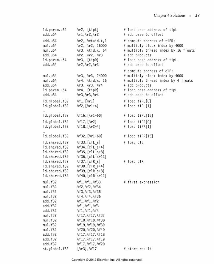
ld.param.u64 %r2, [tipL] # load base address of tipLadd.u64 %r1,%r2,%r2 # add base to offset
add.u64 %r2, %ctaid.x,1 # compute address of tiPR:mul.u64 %r2, %r2, 16000 # multiply block index by 4000mul.u64 %r3, %tid.x, 64 # multiply thread index by 16 floatsadd.u64 %r2, %r2, %r3 # add productsld.param.u64 %r3, [tipR] # load base address of tipLadd.u64 %r2,%r2,%r3 # add base to offset
# compute address of clP:mul.u64 %r3, %r3, 24000 # multiply block index by 4000mul.u64 %r4, %tid.x, 16 # multiply thread index by 4 floatsadd.u64 %r3, %r3, %r4 # add productsld.param.u64 %r4, [tipR] # load base address of tipLadd.u64 %r3,%r3,%r4 # add base to offset
ld.global.f32 %f1,[%r1] # load tiPL[0]ld.global.f32 %f2,[%r1+4] # load tiPL[1]…ld.global.f32 %f16,[%r1+60] # load tiPL[15]
ld.global.f32 %f17,[%r2] # load tiPR[0]ld.global.f32 %f18,[%r2+4] # load tiPR[1]…ld.global.f32 %f32,[%r1+60] # load tiPR[15]
ld.shared.f32 %f33,[clL_s] # load clLld.shared.f32 %f34,[clL_s+4]ld.shared.f32 %f35,[clL_s+8]ld.shared.f32 %f36,[clL_s+12]ld.shared.f32 %f37,[clR_s] # load clRld.shared.f32 %f38,[clR_s+4]ld.shared.f32 %f39,[clR_s+8]ld.shared.f32 %f40,[clR_s+12]
mul.f32 %f1,%f1,%f33 # first expressionmul.f32 %f2,%f2,%f34mul.f32 %f3,%f3,%f35mul.f32 %f4,%f4,%f36add.f32 %f1,%f1,%f2add.f32 %f1,%f1,%f3add.f32 %f1,%f1,%f4mul.f32 %f17,%f17,%f37mul.f32 %f18,%f18,%f38mul.f32 %f19,%f19,%f39mul.f32 %f20,%f20,%f40add.f32 %f17,%f17,%f18add.f32 %f17,%f17,%f19add.f32 %f17,%f17,%f20st.global.f32 [%r3],%f17 # store result
Copyright © 2012 Elsevier, Inc. All rights reserved.

38 ■ Solutions to Case Studies and Exercises
mul.f32 %f5,%f5,%f33 # second expressionmul.f32 %f6,%f6,%f34mul.f32 %f7,%f7,%f35mul.f32 %f8,%f8,%f36add.f32 %f5,%f5,%f6add.f32 %f5,%f5,%f7add.f32 %f5,%f5,%f8mul.f32 %f21,%f21,%f37mul.f32 %f22,%f22,%f38mul.f32 %f23,%f23,%f39mul.f32 %f24,%f24,%f40add.f32 %f21,%f21,%f22add.f32 %f21,%f21,%f23add.f32 %f21,%f21,%f24st.global.f32 [%r3+4],%f21 # store result
mul.f32 %f9,%f9,%f33 # third expressionmul.f32 %f10,%f10,%f34mul.f32 %f11,%11,%f35mul.f32 %f12,%f12,%f36add.f32 %f9,%f9,%f10add.f32 %f9,%f9,%f11add.f32 %f9,%f9,%f12mul.f32 %f25,%f25,%f37mul.f32 %f26,%f26,%f38mul.f32 %f27,%f27,%f39mul.f32 %f28,%f28,%f40add.f32 %f25,%f26,%f22add.f32 %f25,%f27,%f23add.f32 %f25,%f28,%f24st.global.f32 [%r3+8],%f25 # store result
mul.f32 %f13,%f13,%f33 # fourth expressionmul.f32 %f14,%f14,%f34mul.f32 %f15,%f15,%f35mul.f32 %f16,%f16,%f36add.f32 %f13,%f14,%f6add.f32 %f13,%f15,%f7add.f32 %f13,%f16,%f8mul.f32 %f29,%f29,%f37mul.f32 %f30,%f30,%f38mul.f32 %f31,%f31,%f39mul.f32 %f32,%f32,%f40add.f32 %f29,%f29,%f30add.f32 %f29,%f29,%f31add.f32 %f29,%f29,%f32st.global.f32 [%r3+12],%f29 # store result
Copyright © 2012 Elsevier, Inc. All rights reserved.

Chapter 4 Solutions ■ 39
4.8 It will perform well, since there are no branch divergences, all memory referencesare coalesced, and there are 500 threads spread across 6 blocks (3000 total threads),which provides many instructions to hide memory latency.
Exercises
4.9 a. This code reads four floats and writes two floats for every six FLOPs, soarithmetic intensity = 6/6 = 1.
b. Assume MVL = 64:
li $VL,44 # perform the first 44 opsli $r1,0 # initialize index
loop: lv $v1,a_re+$r1 # load a_relv $v3,b_re+$r1 # load b_remulvv.s $v5,$v1,$v3 # a+re*b_relv $v2,a_im+$r1 # load a_im
lv $v4,b_im+$r1 # load b_immulvv.s $v6,$v2,$v4 # a+im*b_imsubvv.s $v5,$v5,$v6 # a+re*b_re - a+im*b_imsv $v5,c_re+$r1 # store c_remulvv.s $v5,$v1,$v4 # a+re*b_immulvv.s $v6,$v2,$v3 # a+im*b_readdvv.s $v5,$v5,$v6 # a+re*b_im + a+im*b_resv $v5,c_im+$r1 # store c_imbne $r1,0,else # check if first iterationaddi $r1,$r1,#44 # first iteration,
increment by 44j loop # guaranteed next iteration
else: addi $r1,$r1,#256 # not first iteration, increment by 256
skip: blt $r1,1200,loop # next iteration?
c.
1. mulvv.s lv # a_re * b_re (assume already # loaded), load a_im
2. lv mulvv.s # load b_im, a_im*b_im3. subvv.s sv # subtract and store c _re4. mulvv.s lv # a_re*b_im, load next a_re vector5. mulvv.s lv # a_im*b_re, load next b_re vector6. addvv.s sv # add and store c_im
6 chimes
Copyright © 2012 Elsevier, Inc. All rights reserved.

40 ■ Solutions to Case Studies and Exercises
d. total cycles per iteration =
6 chimes × 64 elements + 15 cycles (load/store) × 6 + 8 cycles (multiply) ×4 + 5 cycles (add/subtract) × 2 = 516
cycles per result = 516/128 = 4
e.
1. mulvv.s # a_re*b_re2. mulvv.s # a_im*b_im3. subvv.s sv # subtract and store c_re4. mulvv.s # a_re*b_im5. mulvv.s lv # a_im*b_re, load next a_re6. addvv.s sv lv lv lv # add, store c_im, load next b_re,a_im,b_im
Same cycles per result as in part c. Adding additional load/store units did notimprove performance.
4.10 Vector processor requires:
■ (200 MB + 100 MB)/(30 GB/s) = 10 ms for vector memory access +
■ 400 ms for scalar execution.
Assuming that vector computation can be overlapped with memory access, totaltime = 410 ms.
The hybrid system requires:
■ (200 MB + 100 MB)/(150 GB/s) = 2 ms for vector memory access +
■ 400 ms for scalar execution +
■ (200 MB + 100 MB)/(10 GB/s) = 30 ms for host I/O
Even if host I/O can be overlapped with GPU execution, the GPU will require430 ms and therefore will achieve lower performance than the host.
4.11 a. for (i=0;i<32;i+=2) dot[i] = dot[i]+dot[i+1];for (i=0;i<16;i+=4) dot[i] = dot[i]+dot[i+2];for (i=0;i<8;i+=8) dot[i] = dot[i]+dot[i+4];for (i=0;i<4;i+=16) dot[i] = dot[i]+dot[i+8];for (i=0;i<2;i+=32) dot[i] = dot[i]+dot[i+16];dot[0]=dot[0]+dot[32];
b. li $VL,4addvv.s $v0(0),$v0(4)addvv.s $v0(8),$v0(12)addvv.s $v0(16),$v0(20)addvv.s $v0(24),$v0(28)addvv.s $v0(32),$v0(36)addvv.s $v0(40),$v0(44)addvv.s $v0(48),$v0(52)addvv.s $v0(56),$v0(60)
Copyright © 2012 Elsevier, Inc. All rights reserved.

Chapter 4 Solutions ■ 41
c. for (unsigned int s= blockDim.x/2;s>0;s/=2) {if (tid<s) sdata[tid]=sdata[tid]+sdata[tid+s]; __syncthreads();}
4.12 a. Reads 40 bytes and writes 4 bytes for every 8 FLOPs, thus 8/44 FLOPs/byte.
b. This code performs indirect references through the Ca and Cb arrays, as theyare indexed using the contents of the IDx array, which can only be performedat runtime. While this complicates SIMD implementation, it is still possibleto perform type of indexing using gather-type load instructions. The inner-most loop (iterates on z) can be vectorized: the values for Ex, dH1, dH2, Ca,and Cb could be operated on as SIMD registers or vectors. Thus this code isamenable to SIMD and vector execution.
c. Having an arithmetic intensity of 0.18, if the processor has a peak floating-point throughout > (30 GB/s) × (0.18 FLOPs/byte) = 5.4 GFLOPs/s, then thiscode is likely to be memory-bound, unless the working set fits well within theprocessor’s cache.
d. The single precision arithmetic intensity corresponding to the edge of the roofis 85/4 = 21.25 FLOPs/byte.
4.13 a. 1.5 GHz × .80 × .85 × 0.70 × 10 cores × 32/4 = 57.12 GFLOPs/s
b. Option 1:
1.5 GHz × .80 × .85 × .70 × 10 cores × 32/2 = 114.24 GFLOPs/s (speedup =114.24/57.12 = 2)
Option 2:
1.5 GHz × .80 × .85 × .70 × 15 cores × 32/4 = 85.68 GFLOPs/s (speedup =85.68/57.12 = 1.5)
Option 3:
1.5 GHz × .80 × .95 × .70 × 10 cores × 32/4 = 63.84 GFLOPs/s (speedup =63.84/57.12 = 1.11)
Option 3 is best.
4.14 a. Using the GCD test, a dependency exists if GCD (2,4) must divide 5 – 4. Inthis case, a loop-carried dependency does exist.
b. Output dependencies
S1 and S3 cause through A[i]
Anti-dependencies
S4 and S3 cause an anti-dependency through C[i]
Re-written code
for (i=0;i<100;i++) { T[i] = A[i] * B[i]; /* S1 */ B[i] = T[i] + c; /* S2 */ A1[i] = C[i] * c; /* S3 */ C1[i] = D[i] * A1[i]; /* S4 */}
Copyright © 2012 Elsevier, Inc. All rights reserved.
42 ■ Solutions to Case Studies and Exercises
True dependencies
S4 and S3 through A[i]
S2 and S1 through T[i]
c. There is an anti-dependence between iteration i and i+1 for array B. This canbe avoided by renaming the B array in S2.
4.15 a. Branch divergence: causes SIMD lanes to be masked when threads followdifferent control paths
b. Covering memory latency: a sufficient number of active threads can hidememory latency and increase instruction issue rate
c. Coalesced off-chip memory references: memory accesses should be orga-nized consecutively within SIMD thread groups
d. Use of on-chip memory: memory references with locality should take advan-tage of on-chip memory, references to on-chip memory within a SIMD threadgroup should be organized to avoid bank conflicts
4.16 This GPU has a peak throughput of 1.5 × 16 × 16 = 384 GFLOPS/s of single-precision throughput. However, assuming each single precision operation requiresfour-byte two operands and outputs one four-byte result, sustaining this throughput(assuming no temporal locality) would require 12 bytes/FLOP × 384 GFLOPs/s =4.6 TB/s of memory bandwidth. As such, this throughput is not sustainable, but canstill be achieved in short bursts when using on-chip memory.
4.17 Reference code for programming exercise:
#include <stdio.h>#include <stdlib.h>#include <sys/time.h>#include <cuda.h>
__global__ void life (unsigned char *d_board,int iterations) { int i,row,col,rows,cols; unsigned char state,neighbors;
row = blockIdx.y * blockDim.y + threadIdx.y; col = blockIdx.x * blockDim.x + threadIdx.x; rows = gridDim.y * blockDim.y; cols = gridDim.x * blockDim.x;
state = d_board[(row)*cols+(col)];
for (i=0;i<iterations;i++) { neighbors=0;
if (row!=0) {if (col!=0) if (d_board[(row-1)*cols+(col-1)]==1) neighbors++;if (d_board[(row-1)*cols+(col)]==1) neighbors++;if (col!=(cols-1)) if (d_board[(row-1)*cols+(col+1)]==1) neighbors++;
}
if (col!=0) if (d_board[(row)*cols+(col-1)]==1) neighbors++;
Copyright © 2012 Elsevier, Inc. All rights reserved.

Chapter 4 Solutions ■ 43
if (col!=(cols-1)) if (d_board[(row)*cols+(col+1)]==1) neighbors++;
if (row!=(rows-1)) {if (col!=0) if (d_board[(row+1)*cols+(col-1)]==1) neighbors++;if (d_board[(row+1)*cols+(col)]==1) neighbors++;if (col!=(cols-1)) if (d_board[(row+1)*cols+(col+1)]==1) neighbors++;
}
if (neighbors<2) state = 0;else if (neighbors==3) state = 1;else if (neighbors>3) state = 0;
__syncthreads();
d_board[(row)*cols+(col)]=state; }}
int main () { dim3 gDim,bDim; unsigned char *h_board,*d_board; int i,iterations=100;
bDim.y=16; bDim.x=32; bDim.z=1;
gDim.y=16; gDim.x=8; gDim.z=1;
h_board=(unsigned char *)malloc(sizeof(unsigned char)*4096*4096); cudaMalloc((void **)&d_board,sizeof(unsigned char)*4096*4096);
srand(56); for (i=0;i<4096*4096;i++) h_board[i]=rand()%2;
cudaMemcpy(d_board,h_board,sizeof(unsigned char)*4096*4096,cudaMemcpyHostToDevice);
life <<<gDim,bDim>>> (d_board,iterations);
cudaMemcpy(h_board,d_board,sizeof(unsigned char)*4096*4096,cudaMemcpyDeviceToHost);
free(h_board); cudaFree(d_board);}
Copyright © 2012 Elsevier, Inc. All rights reserved.
44 ■ Solutions to Case Studies and Exercises
Case Study 1: Single-Chip Multicore Multiprocessor
5.1 a. P0: read 120 P0.B0: (S, 120, 0020) returns 0020
b. P0: write 120 80 P0.B0: (M, 120, 0080)
P3.B0: (I, 120, 0020)
c. P3: write 120 80 P3.B0: (M, 120, 0080)
d. P1: read 110 P1.B2: (S, 110, 0010) returns 0010
e. P0: write 108 48 P0.B1: (M, 108, 0048)
P3.B1: (I, 108, 0008)
f. P0: write 130 78 P0.B2: (M, 130, 0078)
M: 110 0030 (writeback to memory)
g. P3: write 130 78 P3.B2: (M, 130, 0078)
5.2 a. P0: read 120, Read miss, satisfied by memory
P0: read 128, Read miss, satisfied by P1’s cache
P0: read 130, Read miss, satisfied by memory, writeback 110
Implementation 1: 100 + 40 + 10 + 100 + 10 = 260 stall cycles
Implementation 2: 100 + 130 + 10 + 100 + 10 = 350 stall cycles
b. P0: read 100, Read miss, satisfied by memory
P0: write 108 48, Write hit, sends invalidate
P0: write 130 78, Write miss, satisfied by memory, write back 110
Implementation 1: 100 + 15 + 10 + 100 = 225 stall cycles
Implementation 2: 100 + 15 + 10 + 100 = 225 stall cycles
c. P1: read 120, Read miss, satisfied by memory
P1: read 128, Read hit
P1: read 130, Read miss, satisfied by memory
Implementation 1: 100 + 0 + 100 = 200 stall cycles
Implementation 2: 100 + 0 + 100 = 200 stall cycles
d. P1: read 100, Read miss, satisfied by memory
P1: write 108 48, Write miss, satisfied by memory, write back 128
P1: write 130 78, Write miss, satisfied by memory
Implementation 1: 100 + 100 + 10 + 100 = 310 stall cycles
Implementation 2: 100 + 100 + 10 + 100 = 310 stall cycles
5.3 See Figure S.28
Chapter 5 Solutions
Copyright © 2012 Elsevier, Inc. All rights reserved.

Chapter 5 Solutions ■ 45
5.4 (Showing results for implementation 1)
a. P1: read 110, Read miss, P0’s cache
P3: read 110, Read miss, MSI satisfies in memory, MOSI satisfies in P0’scache
P0: read 110, Read hit
MSI: 40 + 10 + 100 + 0 = 150 stall cycles
MOSI: 40 + 10 + 40 + 10 + 0 = 100 stall cycles
b. P1: read 120, Read miss, satisfied in memory
P3: read 120, Read hit
P0: read 120, Read miss, satisfied in memory
Both protocols: 100 + 0 + 100 = 200 stall cycles
c. P0: write 120 80, Write miss, invalidates P3
P3: read 120, Read miss, P0’s cache
P0: read 120, Read hit
Both protocols: 100 + 40 + 10 + 0 = 150 stall cycles
Figure S.28 Protocol diagram.
Modified
CPU write hitCPU read hit
CPU write
Pla
ce w
rite
mis
s o
n b
us
Place
inva
lidat
e
on bus CPU w
rite
Place read miss on busCPU read
Write miss or invalidatefor this block
Write miss forthis block
Read miss
Invalidate for this block
Write m
iss for this block
Writeback block; abort m
emory access
CPU writePlace invalidate on bus
Writeback block; abort memory access
Wri
teb
ack
blo
ck;
abo
rt m
emo
ry a
cces
s
Owned
Invalid Shared
CPU read hit
CPU read hit
Copyright © 2012 Elsevier, Inc. All rights reserved.

46 ■ Solutions to Case Studies and Exercises
d. P0: write 108 88, Send invalidate, invalidate P3
P3: read 108, Read miss, P0’s cache
P0: write 108 98, Send invalidate, invalidate P3
Both protocols: 15 + 40 + 10 + 15 = 80 stall cycles
5.5 See Figure S.29
5.6 a. p0: read 100, Read miss, satisfied in memory, no sharers MSI: S, MESI: E
p0: write 100 40, MSI: send invalidate, MESI: silent transition from E to M
MSI: 100 + 15 = 115 stall cycles
MESI: 100 + 0 = 100 stall cycles
b. p0: read 120, Read miss, satisfied in memory, sharers both to S
p0: write 120 60, Both send invalidates
Both: 100 + 15 = 115 stall cycles
c. p0: read 100, Read miss, satisfied in memory, no sharers MSI: S, MESI: E
p0: read 120, Read miss, memory, silently replace 120 from S or E
Both: 100 + 100 = 200 stall cycles, silent replacement from E
Figure S.29 Diagram for a MESI protocol.
Modified
CPU write hitCPU read hit
CP
U w
rite
Pla
ce w
rite
mis
s o
n b
us
CPU writ
e
Place
inva
lidat
e
on bus
Place read miss on busCPU read, other shared block
Write miss or invalidatefor this block
CPU write hit
Writ
e m
iss
for
this
blo
ckW
rite
bac
k b
lock
;ab
ort
mem
ory
acc
ess
Writ
ebac
k blo
ck;
abort
mem
ory
acce
ss
Read
miss
Excl.
Invalid Shared
CPU read hit
CPU read hit
Rea
d m
iss
Place read miss on bus
CPU read, no shares
Write m
iss or invalidate for this block
Copyright © 2012 Elsevier, Inc. All rights reserved.

Chapter 5 Solutions ■ 47
d. p0: read 100, Read miss, satisfied in memory, no sharers MSI: S, MESI: E
p1: write 100 60, Write miss, satisfied in memory regardless of protocol
Both: 100 + 100 = 200 stall cycles, don’t supply data in E state (someprotocols do)
e. p0: read 100, Read miss, satisfied in memory, no sharers MSI: S, MESI: E
p0: write 100 60, MSI: send invalidate, MESI: silent transition from E to M
p1: write 100 40, Write miss, P0’s cache, writeback data to memory
MSI: 100 + 15 + 40 + 10 = 165 stall cycles
MESI: 100 + 0 + 40 + 10 = 150 stall cycles
5.7 a. Assume the processors acquire the lock in order. P0 will acquire it first, incur-ring 100 stall cycles to retrieve the block from memory. P1 and P3 will stalluntil P0’s critical section ends (ping-ponging the block back and forth) 1000cycles later. P0 will stall for (about) 40 cycles while it fetches the block toinvalidate it; then P1 takes 40 cycles to acquire it. P1’s critical section is 1000cycles, plus 40 to handle the write miss at release. Finally, P3 grabs the blockfor a final 40 cycles of stall. So, P0 stalls for 100 cycles to acquire, 10 to giveit to P1, 40 to release the lock, and a final 10 to hand it off to P1, for a total of160 stall cycles. P1 essentially stalls until P0 releases the lock, which will be100 + 1000 + 10 + 40 = 1150 cycles, plus 40 to get the lock, 10 to give it toP3, 40 to get it back to release the lock, and a final 10 to hand it back to P3.This is a total of 1250 stall cycles. P3 stalls until P1 hands it off the releasedlock, which will be 1150 + 40 + 10 + 1000 + 40 = 2240 cycles. Finally, P3gets the lock 40 cycles later, so it stalls a total of 2280 cycles.
b. The optimized spin lock will have many fewer stall cycles than the regularspin lock because it spends most of the critical section sitting in a spin loop(which while useless, is not defined as a stall cycle). Using the analysis belowfor the interconnect transactions, the stall cycles will be 3 read memory misses(300), 1 upgrade (15) and 1 write miss to a cache (40 + 10) and 1 write miss tomemory (100), 1 read cache miss to cache (40 + 10), 1 write miss to memory(100), 1 read miss to cache and 1 read miss to memory (40 + 10 + 100),followed by an upgrade (15) and a write miss to cache (40 + 10), and finally awrite miss to cache (40 + 10) followed by a read miss to cache (40 + 10) andan upgrade (15). So approximately 945 cycles total.
c. Approximately 31 interconnect transactions. The first processor to win arbi-tration for the interconnect gets the block on its first try (1); the other twoping-pong the block back and forth during the critical section. Because thelatency is 40 cycles, this will occur about 25 times (25). The first processordoes a write to release the lock, causing another bus transaction (1), and thesecond processor does a transaction to perform its test and set (1). The lastprocessor gets the block (1) and spins on it until the second processor releasesit (1). Finally the last processor grabs the block (1).
Copyright © 2012 Elsevier, Inc. All rights reserved.
48 ■ Solutions to Case Studies and Exercises
d. Approximately 15 interconnect transactions. Assume processors acquire thelock in order. All three processors do a test, causing a read miss, then a testand set, causing the first processor to upgrade and the other two to writemiss (6). The losers sit in the test loop, and one of them needs to get back ashared block first (1). When the first processor releases the lock, it takes awrite miss (1) and then the two losers take read misses (2). Both have theirtest succeed, so the new winner does an upgrade and the new loser takes awrite miss (2). The loser spins on an exclusive block until the winner releasesthe lock (1). The loser first tests the block (1) and then test-and-sets it, whichrequires an upgrade (1).
5.8 Latencies in implementation 1 of Figure 5.36 are used.
a. P0: write 110 80 Hit in P0’s cache, no stall cycles for either TSO or SC
P0: read 108 Hit in P0’s cache, no stall cycles for either TSO or SC
b. P0: write 100 80 Miss, TSO satisfies write in write buffer (0 stall cycles)SC must wait until it receives the data (100 stall cycles)
P0: read 108 Hit, but must wait for preceding operation: TSO = 0,SC = 100
c. P0: write 110 80 Hit in P0’s cache, no stall cycles for either TSO or SC
P0: write 100 90 Miss, TSO satisfies write in write buffer (0 stallcycles) SC must wait until it receives the data (100stall cycles)
d. P0: write 100 80 Miss, TSO satisfies write in write buffer (0 stallcycles) SC must wait until it receives the data (100 stall cycles)
P0: write 110 90 Hit, but must wait for preceding operation: TSO = 0, SC = 100
Case Study 2: Simple Directory-Based Coherence
5.9 a. P0,0: read 100 L1 hit returns 0x0010, state unchanged (M)
b. P0,0: read 128 L1 miss and L2 miss will replace B1 in L1 and B1 inL2 which has address 108.
L1 will have 128 in B1 (shared), L2 also will have it(DS, P0,0)
Memory directory entry for 108 will become <DS, C1>
Memory directory entry for 128 will become <DS, C0>
c, d, …, h: follow same approach
Copyright © 2012 Elsevier, Inc. All rights reserved.

Chapter 5 Solutions ■ 49
5.10 a. P0,0: write 100 80, Write hit only seen by P0,0
b. P0,0: write 108 88, Write “upgrade” received by P0,0; invalidate receivedby P3,1
c. P0,0: write 118 90, Write miss received by P0,0; invalidate received by P1,0
d. P1,0: write 128 98, Write miss received by P1,0.
5.11 a. See Figures S.30 and S.31
5.12 The Exclusive state (E) combines properties of Modified (M) and Shared (S).The E state allows silent upgrades to M, allowing the processor to write the blockwithout communicating this fact to memory. It also allows silent downgrades to I,allowing the processor to discard its copy with notifying memory. The memorymust have a way of inferring either of these transitions. In a directory-based system,this is typically done by having the directory assume that the node is in state M andforwarding all misses to that node. If a node has silently downgraded to I, then itsends a NACK (Negative Acknowledgment) back to the directory, which theninfers that the downgrade occurred. However, this results in a race with other mes-sages, which can cause other problems.
Figure S.30 Cache states.
Modified
CPU write hitCPU read hit
Sen
d w
rite
mis
s m
essa
ge
CPU writ
e
Send in
valid
ate
mes
sage
CPU readSend read message
Invalidate
CPU write
CPU write missWrite data backWrite miss
CPU writeSend invalidate message
Read missSend data
Fet
ch in
valid
ate
Wri
te d
ata
bac
k
Fetch
Writ
e dat
a bac
k
Owned
Invalid Shared
CPU read hit
CPU read missCPU write missWrite data backRead miss
CPU read missRead miss
CPU read hit
Write data back
Fetch invalidate
Invalidate
Copyright © 2012 Elsevier, Inc. All rights reserved.

50 ■ Solutions to Case Studies and Exercises
Case Study 3: Advanced Directory Protocol
5.13 a. P0,0: read 100 Read hit
b. P0,0: read 120 Miss, will replace modified data (B0) and get new linein shared state
P0,0: M MIA I ISD S Dir: DM {P0,0} DI {}
c. P0,0: write 120 80 Miss will replace modified data (B0) and get new linein modified state
P0,0: M MIA I IMAD IMA M
P3,1: S I
Dir: DS {P3,0} DM {P0,0}
d, e, f: steps similar to parts a, b, and c
5.14 a. P0,0: read 120 Miss, will replace modified data (B0) and get new linein shared state
P0,0: M MIA I ISD S
Figure S.31 Directory states.
Modified
Write missFetch invalidateData value responseSharers = {P}
Writ
e m
iss
Dat
a va
lue
rep
lyS
har
ers
={P
}
Writ
e m
iss
Send in
valid
ate
mes
sage
to s
harer
s
Data
valu
e re
ply
Sharer
s= {P}
Data value reply,Sharers = {P}
Read miss
Write missFetch invalidateData value responseSharers = {P}
Read missFetch; Data value replySharers = sharers + {P}
Dat
a w
rite
back
Sh
arer
s=
{}
Dat
a w
rite
back
Sh
arer
s=
shar
ers
– {P
}
Owned
Invalid Shared
Read missFetchData value responseSharers = sharers + {P}
Read missData value replySharers = sharers + {P}
Copyright © 2012 Elsevier, Inc. All rights reserved.
Chapter 5 Solutions ■ 51
P1,0: read 120 Miss, will replace modified data (B0) and get new linein shared state
P1,0: M MIA I ISD S
Dir: DS {P3,0} DS {P3,0; P0,0} DS {P3,0;P0,0; P1,0}
b. P0,0: read 120 Miss, will replace modified data (B0) and get new linein shared state
P0,0: M MIA I ISD S
P1,0: write 120 80 Miss will replace modified data (B0) and get new linein modified state
P1,0: M MIA I IMAD IMA M
P3,1: S I
Dir: DS {P3,1} DS {P3,0; P1,0} DM {P1,0}
c, d, e: steps similar to parts a and b
5.15 a. P0,0: read 100 Read hit, 1 cycle
b. P0,0: read 120 Read Miss, causes modified block replacement and issatisfied in memory and incurs 4 chip crossings(see underlined)
Latency for P0,0: Lsend_data + Ldata_msg + Lwrite_memory + Linv +L_ack + Lreq_msg + Lsend_msg + Lreq_msg + Lread_memory + Ldata_msg + Lrcv_data + 4 × chip crossings latency = 20 + 30 + 20 + 1 +4 + 15 + 6 + 15 + 100 + 30 + 15 + 4 × 20 = 336
c, d, e: follow same steps as a and b
5.16 All protocols must ensure forward progress, even under worst-case memory accesspatterns. It is crucial that the protocol implementation guarantee (at least with aprobabilistic argument) that a processor will be able to perform at least one mem-ory operation each time it completes a cache miss. Otherwise, starvation mightresult. Consider the simple spin lock code:
tas: DADDUI R2, R0, #1lockit: EXCH R2, 0(R1)BNEZ R2, lockit
If all processors are spinning on the same loop, they will all repeatedly issueGetM messages. If a processor is not guaranteed to be able to perform at least oneinstruction, then each could steal the block from the other repeatedly. In the worstcase, no processor could ever successfully perform the exchange.
Copyright © 2012 Elsevier, Inc. All rights reserved.

52 ■ Solutions to Case Studies and Exercises
5.17 a. The MSA state is essentially a “transient O” because it allows the processor toread the data and it will respond to GetShared and GetModified requests fromother processors. It is transient, and not a real O state, because memory willsend the PutM_Ack and take responsibility for future requests.
b. See Figures S.32 and S.33
State Read WriteReplace-ment INV
Forwarded_GetS
Forwarded_GetM
PutM_Ack Data Last ACK
I send GetS/IS
send GetM/IM
error sendAck/I
error error error error error
S do Read send GetM/IM
I sendAck/I
error error error error error
O do Read send GetM/OM
send PutM/OI
error send Data send Data/I error — —
M do Read do Write send PutM/MI
error send Data/O send Data/I error error error
IS z z z sendAck/ISI
error error error save Data, do Read/S
error
ISI z z z send Ack error error error save Data, do Read/I
error
IM z z z send Ack IMO IMIA error save Data do Write/M
IMI z z z error error error error save Data do Write, send Data/I
IMO z z z sendAck/IMI
— IMOI error save Data do Write, send Data/O
IMOI z z z error error error error save Data do Write, send Data/I
OI z z z error send Data send Data /I error error
MI z z z error send Data send Data /I error error
OM z z z error send Data send Data/IM error save Data do Write/M
Figure S.32 Directory protocol cache controller transitions.
State Read WriteReplacement(owner)
INV(nonowner)
DI send Data, add to sharers/DS
send Data, clear sharers, set owner/DM
error send PutM_Ack
DS send Data, add to sharers
send INVs to sharers, clear sharers, set owner, send Data/DM
error send PutM_Ack
DO forward GetS, add to sharers
forward GetM, send INVs to sharers, clear sharers, set owner/DM
send Data, send PutM_Ack/DS
send PutM_Ack
DM forward GetS, add to requester and owner to sharers/DO
forward GetM, send INVs to sharers, clear sharers, set owner
send Data, send PutM_Ack/DI
send PutM_Ack
Figure S.33 Directory controller transitions.
Copyright © 2012 Elsevier, Inc. All rights reserved.

Chapter 5 Solutions ■ 53
5.18 a. P1,0: read 100
P3,1: write 100 90
In this problem, both P0,1 and P3,1 miss and send requests that race to thedirectory. Assuming that P0,1’s GetS request arrives first, the directory willforward P0,1’s GetS to P0,0, followed shortly afterwards by P3,1’s GetM. Ifthe network maintains point-to-point order, then P0,0 will see the requests inthe right order and the protocol will work as expected. However, if the for-warded requests arrive out of order, then the GetX will force P0 to state I,causing it to detect an error when P1’s forwarded GetS arrives.
b. P1,0: read 100
P0,0: replace 100
P1,0’s GetS arrives at the directory and is forwarded to P0,0 before P0,0’sPutM message arrives at the directory and sends the PutM_Ack. However, ifthe PutM_Ack arrives at P0,0 out of order (i.e., before the forwarded GetS),then this will cause P0,0 to transition to state I. In this case, the forwardedGetS will be treated as an error condition.
Exercises
5.19 The general form for Amdahl’s Law is
all that needs to be done to compute the formula for speedup in this multiproces-sor case is to derive the new execution time.
The exercise states that for the portion of the original execution time that can usei processors is given by F(i,p). If we let Execution timeold be 1, then the relativetime for the application on p processors is given by summing the times requiredfor each portion of the execution time that can be sped up using i processors,where i is between 1 and p. This yields
Substituting this value for Execution timenew into the speedup equation makesAmdahl’s Law a function of the available processors, p.
5.20 a. (i) 64 processors arranged a as a ring: largest number of communicationhops = 32 communication cost = (100 + 10 × 32) ns = 420 ns.
(ii) 64 processors arranged as 8x8 processor grid: largest number of commu-nication hops = 14 communication cost = (100 + 10 × 14) ns = 240 ns.
(iii) 64 processors arranged as a hypercube: largest number of hops = 6 (log264) communication cost = (100 + 10 × 6) ns = 160 ns.
SpeedupExecution timeold
Execution timenew------------------------------------------------=
Execution timenewf i,p( )
i-------------
i 1=
p
∑=
Copyright © 2012 Elsevier, Inc. All rights reserved.

54 ■ Solutions to Case Studies and Exercises
b. Base CPI = 0.5 cpi
(i) 64 processors arranged a as a ring: Worst case CPI = 0.5 + 0.2/100 ×(420) = 1.34 cpi
(ii) 64 processors arranged as 8x8 processor grid: Worst case CPI = 0.5 + 0.2/100 × (240) = 0.98 cpi
(iii) 64 processors arranged as a hypercube: Worst case CPI CPI = 0.5 + 0.2/100 × (160) = 0.82 cpi
The average CPI can be obtained by replacing the largest number of communi-cations hops in the above calculation by h , the average numbers of communica-tions hops. That latter number depends on both the topology and the application.
c. Since the CPU frequency and the number of instructions executed did notchange, the answer can be obtained by the CPI for each of the topologies(worst case or average) by the base (no remote communication) CPI.
5.21 To keep the figures from becoming cluttered, the coherence protocol is split intotwo parts as was done in Figure 5.6 in the text. Figure S.34 presents theCPU portion of the coherence protocol, and Figure S.35 presents the bus portionof the protocol. In both of these figures, the arcs indicate transitions and the textalong each arc indicates the stimulus (in normal text) and bus action (in bold text)that occurs during the transition between states. Finally, like the text, we assume awrite hit is handled as a write miss.
Figure S.34 presents the behavior of state transitions caused by the CPU itself. Inthis case, a write to a block in either the invalid or shared state causes us to broad-cast a “write invalidate” to flush the block from any other caches that hold theblock and move to the exclusive state. We can leave the exclusive state througheither an invalidate from another processor (which occurs on the bus side of thecoherence protocol state diagram), or a read miss generated by the CPU (whichoccurs when an exclusive block of data is displaced from the cache by a secondblock). In the shared state only a write by the CPU or an invalidate from anotherprocessor can move us out of this state. In the case of transitions caused by eventsexternal to the CPU, the state diagram is fairly simple, as shown in Figure S.35.When another processor writes a block that is resident in our cache, we uncondi-tionally invalidate the corresponding block in our cache. This ensures that thenext time we read the data, we will load the updated value of the block frommemory. Also, whenever the bus sees a read miss, it must change the state of anexclusive block to shared as the block is no longer exclusive to a single cache.
The major change introduced in moving from a write-back to write-throughcache is the elimination of the need to access dirty blocks in another processor’scaches. As a result, in the write-through protocol it is no longer necessary to pro-vide the hardware to force write back on read accesses or to abort pending mem-ory accesses. As memory is updated during any write on a write-through cache, aprocessor that generates a read miss will always retrieve the correct informationfrom memory. Basically, it is not possible for valid cache blocks to be incoherentwith respect to main memory in a system with write-through caches.
Copyright © 2012 Elsevier, Inc. All rights reserved.

Chapter 5 Solutions ■ 55
Figure S.34 CPU portion of the simple cache coherency protocol for write-throughcaches.
Figure S.35 Bus portion of the simple cache coherency protocol for write-throughcaches.
CPUread
CPU read
CPU readmiss
CPU readhit or write
CPU writeInvalidate block CPU write
Invalidate block
Invalid
Exclusive(read/write)
Shared(read only)
Shared(read only)
Write missInvalidate block
Invalid
Exclusive(read/write)
Write missInvalidate block
Read miss
Copyright © 2012 Elsevier, Inc. All rights reserved.

56 ■ Solutions to Case Studies and Exercises
5.22 To augment the snooping protocol of Figure 5.7 with a Clean Exclusive state weassume that the cache can distinguish a read miss that will allocate a block destinedto have the Clean Exclusive state from a read miss that will deliver a Shared block.Without further discussion we assume that there is some mechanism to do so.
The three states of Figure 5.7 and the transitions between them are unchanged,with the possible clarifying exception of renaming the Exclusive (read/write)state to Dirty Exclusive (read/write).
The new Clean Exclusive (read only) state should be added to the diagram alongwith the following transitions.
■ from Clean Exclusive to Clean Exclusive in the event of a CPU read hit onthis block or a CPU read miss on a Dirty Exclusive block
■ from Clean Exclusive to Shared in the event of a CPU read miss on a Sharedblock or on a Clean Exclusive block
■ from Clean Exclusive to Shared in the event of a read miss on the bus for thisblock
■ from Clean Exclusive to Invalid in the event of a write miss on the bus for thisblock
■ from Clean Exclusive to Dirty Exclusive in the event of a CPU write hit onthis block or a CPU write miss
■ from Dirty Exclusive to Clean Exclusive in the event of a CPU read miss on aDirty Exclusive block
■ from Invalid to Clean Exclusive in the event of a CPU read miss on a DirtyExclusive block
■ from Shared to Clean Exclusive in the event of a CPU read miss on a DirtyExclusive block
Several transitions from the original protocol must change to accommodate the existence of the Clean Exclusive state. The following three transitions are those that change.
■ from Dirty Exclusive to Shared, the label changes to CPU read miss on aShared block
■ from Invalid to Shared, the label changes to CPU miss on a Shared block
■ from Shared to Shared, the miss transition label changes to CPU read miss ona Shared block
5.23 An obvious complication introduced by providing a valid bit per word is the needto match not only the tag of the block but also the offset within the block whensnooping the bus. This is easy, involving just looking at a few more bits. In addi-tion, however, the cache must be changed to support write-back of partial cacheblocks. When writing back a block, only those words that are valid should be writ-ten to memory because the contents of invalid words are not necessarily coherent
Copyright © 2012 Elsevier, Inc. All rights reserved.

Chapter 5 Solutions ■ 57
with the system. Finally, given that the state machine of Figure 5.7 is applied ateach cache block, there must be a way to allow this diagram to apply when statecan be different from word to word within a block. The easiest way to do this wouldbe to provide the state information of the figure for each word in the block. Doingso would require much more than one valid bit per word, though. Without replica-tion of state information the only solution is to change the coherence protocolslightly.
5.24 a. The instruction execution component would be significantly sped up becausethe out-of-order execution and multiple instruction issue allows the latency ofthis component to be overlapped. The cache access component would be sim-ilarly sped up due to overlap with other instructions, but since cache accessestake longer than functional unit latencies, they would need more instructionsto be issued in parallel to overlap their entire latency. So the speedup for thiscomponent would be lower.
The memory access time component would also be improved, but thespeedup here would be lower than the previous two cases. Because the mem-ory comprises local and remote memory accesses and possibly other cache-to-cache transfers, the latencies of these operations are likely to be very high(100’s of processor cycles). The 64-entry instruction window in this exampleis not likely to allow enough instructions to overlap with such long latencies.There is, however, one case when large latencies can be overlapped: whenthey are hidden under other long latency operations. This leads to a techniquecalled miss-clustering that has been the subject of some compiler optimiza-tions. The other-stall component would generally be improved because theymainly consist of resource stalls, branch mispredictions, and the like. Thesynchronization component if any will not be sped up much.
b. Memory stall time and instruction miss stall time dominate the execution forOLTP, more so than for the other benchmarks. Both of these components arenot very well addressed by out-of-order execution. Hence the OLTP workloadhas lower speedup compared to the other benchmarks with System B.
5.25 Because false sharing occurs when both the data object size is smaller than thegranularity of cache block valid bit(s) coverage and more than one data object isstored in the same cache block frame in memory, there are two ways to preventfalse sharing. Changing the cache block size or the amount of the cache block cov-ered by a given valid bit are hardware changes and outside the scope of this exer-cise. However, the allocation of memory locations to data objects is a softwareissue.
The goal is to locate data objects so that only one truly shared object occurs percache block frame in memory and that no non-shared objects are located in thesame cache block frame as any shared object. If this is done, then even with just asingle valid bit per cache block, false sharing is impossible. Note that shared,read-only-access objects could be combined in a single cache block and not con-tribute to the false sharing problem because such a cache block can be held bymany caches and accessed as needed without an invalidations to cause unneces-sary cache misses.
Copyright © 2012 Elsevier, Inc. All rights reserved.

58 ■ Solutions to Case Studies and Exercises
To the extent that shared data objects are explicitly identified in the programsource code, then the compiler should, with knowledge of memory hierarchydetails, be able to avoid placing more than one such object in a cache block framein memory. If shared objects are not declared, then programmer directives mayneed to be added to the program. The remainder of the cache block frame shouldnot contain data that would cause false sharing misses. The sure solution is to padwith block with non-referenced locations.
Padding a cache block frame containing a shared data object with unused mem-ory locations may lead to rather inefficient use of memory space. A cache blockmay contain a shared object plus objects that are read-only as a trade-off betweenmemory use efficiency and incurring some false-sharing misses. This optimiza-tion almost certainly requires programmer analysis to determine if it would beworthwhile. Generally, careful attention to data distribution with respect to cachelines and partitioning the computation across processors is needed.
5.26 The problem illustrates the complexity of cache coherence protocols. In this case,this could mean that the processor P1 evicted that cache block from its cache andimmediately requested the block in subsequent instructions. Given that the write-back message is longer than the request message, with networks that allow out-of-order requests, the new request can arrive before the write back arrives at the direc-tory. One solution to this problem would be to have the directory wait for the writeback and then respond to the request. Alternatively, the directory can send out anegative acknowledgment (NACK). Note that these solutions need to be thoughtout very carefully since they have potential to lead to deadlocks based on the partic-ular implementation details of the system. Formal methods are often used to checkfor races and deadlocks.
5.27 If replacement hints are used, then the CPU replacing a block would send a hint tothe home directory of the replaced block. Such hint would lead the home directoryto remove the CPU from the sharing list for the block. That would save an invali-date message when the block is to be written by some other CPU. Note that whilethe replacement hint might reduce the total protocol latency incurred when writinga block, it does not reduce the protocol traffic (hints consume as much bandwidthas invalidates).
5.28 a. Considering first the storage requirements for nodes that are caches under thedirectory subtree:
The directory at any level will have to allocate entries for all the cache blockscached under that directory’s subtree. In the worst case (all the CPU’s underthe subtree are not sharing any blocks), the directory will have to store asmany entries as the number of blocks of all the caches covered in the subtree.That means that the root directory might have to allocate enough entries toreference all the blocks of all the caches. Every memory block cached in adirectory will represented by an entry <block address, k-bit vector>, the k-bitvector will have a bit specifying all the subtrees that have a copy of the block.For example, for a binary tree an entry <m, 11> means that block m is cachedunder both branches of the tree. To be more precise, one bit per subtree would
Copyright © 2012 Elsevier, Inc. All rights reserved.

Chapter 5 Solutions ■ 59
be adequate if only the valid/invalid states need to be recorded; however torecord whether a block is modified or not, more bits would be needed. Notethat no entry is needed if a block is not cached under the subtree.
If the cache block has m bits (tag + index) then and s state bits need to bestored per block, and the cache can hold b blocks, then the directories atlevel L-1 (lowest level just above CPU’s) will have to hold k × b entries.Each entry will have (m + k × s) bits. Thus each directory at level L-1 willhave (mkb + k2bs) bits. At the next level of the hierarchy, the directorieswill be k times bigger. The number of directories at level i is ki.
To consider memory blocks with a home in the subtree cached outside thesubtree. The storage requirements per directory would have to be modified.Calculation outline:
Note that for some directory (for example the ones at level l-1) the numberof possible home nodes that can be cached outside the subtree is equal to(b × ( kl – x)), where kl is the total number of CPU’s, b is the number ofblocks per cache and x is the number of CPU’s under the directory’s sub-tree. It should be noted that the extra storage diminishes for directories inhigher levels of the tree (for example the directory at level 0 does notrequire any such storage since all the blocks have a home in that direc-tory’s subtree).
b. Simulation.
Figure S.36 Tree-based directory hierarchy (k-ary tree with l levels).
Root (Level 0)Directory
Level 1Directory
Level 1Directory
Level L-1Directory
k-10
CPU0 CPU1 CPUk-1
Copyright © 2012 Elsevier, Inc. All rights reserved.

60 ■ Solutions to Case Studies and Exercises
5.29 Test and set code using load linked and store conditional.
MOV R3, #1LL R2, 0(R1)SC R3, 0(R1)
Typically this code would be put in a loop that spins until a 1 is returned in R3.
5.30 Assume a cache line that has a synchronization variable and the data guarded bythat synchronization variable in the same cache line. Assume a two processor sys-tem with one processor performing multiple writes on the data and the other pro-cessor spinning on the synchronization variable. With an invalidate protocol, falsesharing will mean that every access to the cache line ends up being a miss resultingin significant performance penalties.
5.31 The monitor has to be place at a point through which all memory accesses pass.One suitable place will be in the memory controller at some point where accessesfrom the 4 cores converge (since the accesses are uncached anyways). The monitorwill use some sort of a cache where the tag of each valid entry is the addressaccessed by some load-linked instruction. In the data field of the entry, the corenumber that produced the load-linked access -whose address is stored in the tagfield- is stored.
This is how the monitor reacts to the different memory accesses.
■ Read not originating from a load-linked instruction:
❍ Bypasses the monitor progresses to read data from memory
■ Read originating from a load-linked instruction:
❍ Checks the cache, if there is any entry with whose address matches theread address even if there is a partial address match (for example, read[0:7] and read [4:11] overlap match in addresses [4:7]), the matching cacheentry is invalidated and a new entry is created for the new read (recordingthe core number that it belongs to). If there is no matching entry in thecache, then a new entry is created (if there is space in the cache). In eithercase the read progresses to memory and returns data to originating core.
■ Write not originating from a store-conditional instruction:
❍ Checks the cache, if there is any entry with whose address matches thewrite address even if there is a partial address match (for example, read[0:7] and write [4:11] overlap match in addresses [4:7]), the matchingcache entry is invalidated. The write progresses to memory and writes datato the intended address.
■ Write originating from a store-conditional instruction:
❍ Checks the cache, if there is any entry with whose address matches thewrite address even if there is a partial address match (for example, read[0:7] and write [4:11] overlap match in addresses [4:7]), the core numberin the cache entry is compared to the core that originated the write.
Copyright © 2012 Elsevier, Inc. All rights reserved.

Chapter 5 Solutions ■ 61
If the core numbers are the same, then the matching cache entry is invali-dated, the write proceeds to memory and returns a success signal to theoriginating core. In that case, we expect the address match to be perfect –not partial- as we expect that the same core will not issue load-linked/storeconditional instruction pairs that have overlapping address ranges.
If the core numbers differ, then the matching cache entry is invalidated, thewrite is aborted and returns a failure signal to the originating core. Thiscase signifies that synchronization variable was corrupted by another coreor by some regular store operation.
5.32 a. Because flag is written only after A is written, we would expect C to be 2000,the value of A.
b. Case 1: If the write to flag reached P2 faster than the write to A.
Case 2: If the read to A was faster than the read to flag.
c. Ensure that writes by P1 are carried out in program order and that memoryoperations execute atomically with respect to other memory operations.
To get intuitive results of sequential consistency using barrier instructions, abarrier need to be inserted in P1 between the write to A and the write to flag.
5.33 Inclusion states that each higher level of cache contains all the values present in thelower cache levels, i.e., if a block is in L1 then it is also in L2. The problem statesthat L2 has equal or higher associativity than L1, both use LRU, and both have thesame block size.
When a miss is serviced from memory, the block is placed into all the caches, i.e.,it is placed in L1 and L2. Also, a hit in L1 is recorded in L2 in terms of updatingLRU information. Another key property of LRU is the following. Let A and Bboth be sets whose elements are ordered by their latest use. If A is a subset of Bsuch that they share their most recently used elements, then the LRU element ofB must either be the LRU element of A or not be an element of A.
This simply states that the LRU ordering is the same regardless if there are 10entries or 100. Let us assume that we have a block, D, that is in L1, but not in L2.Since D initially had to be resident in L2, it must have been evicted. At the timeof eviction D must have been the least recently used block. Since an L2 evictiontook place, the processor must have requested a block not resident in L1 andobviously not in L2. The new block from memory was placed in L2 (causing theeviction) and placed in L1 causing yet another eviction. L1 would have pickedthe least recently used block to evict.
Since we know that D is in L1, it must be the LRU entry since it was the LRUentry in L2 by the argument made in the prior paragraph. This means that L1would have had to pick D to evict. This results in D not being in L1 which resultsin a contradiction from what we assumed. If an element is in L1 it has to be in L2(inclusion) given the problem’s assumptions about the cache.
Copyright © 2012 Elsevier, Inc. All rights reserved.
62 ■ Solutions to Case Studies and Exercises
5.34 Analytical models can be used to derive high-level insight on the behavior of thesystem in a very short time. Typically, the biggest challenge is in determining thevalues of the parameters. In addition, while the results from an analytical model cangive a good approximation of the relative trends to expect, there may be significanterrors in the absolute predictions.
Trace-driven simulations typically have better accuracy than analytical models,but need greater time to produce results. The advantages are that this approachcan be fairly accurate when focusing on specific components of the system (e.g.,cache system, memory system, etc.). However, this method does not model theimpact of aggressive processors (mispredicted path) and may not model theactual order of accesses with reordering. Traces can also be very large, often tak-ing gigabytes of storage, and determining sufficient trace length for trustworthyresults is important. It is also hard to generate representative traces from one classof machines that will be valid for all the classes of simulated machines. It is alsoharder to model synchronization on these systems without abstracting the syn-chronization in the traces to their high-level primitives.
Execution-driven simulation models all the system components in detail and isconsequently the most accurate of the three approaches. However, its speed ofsimulation is much slower than that of the other models. In some cases, the extradetail may not be necessary for the particular design parameter of interest.
5.35 One way to devise a multiprocessor/cluster benchmark whose performance getsworse as processors are added:
Create the benchmark such that all processors update the same variable or smallgroup of variables continually after very little computation.
For a multiprocessor, the miss rate and the continuous invalidates in between theaccesses may contribute more to the execution time than the actual computation,and adding more CPU’s could slow the overall execution time.
For a cluster organized as a ring communication costs needed to update the com-mon variables could lead to inverse linear speedup behavior as more processorsare added.
Copyright © 2012 Elsevier, Inc. All rights reserved.


Related Documents