P o w e r E l e c t r o n i c s P o w e r E l e c t r o n i c s Chapter 1 Power Electronic Devices (Part I)

Welcome message from author
This document is posted to help you gain knowledge. Please leave a comment to let me know what you think about it! Share it to your friends and learn new things together.
Transcript
Power ElectronicsPower Electronics
Chapter 1
Power Electronic Devices
(Part I)
Pow
erE
l ect
roni
cs
2
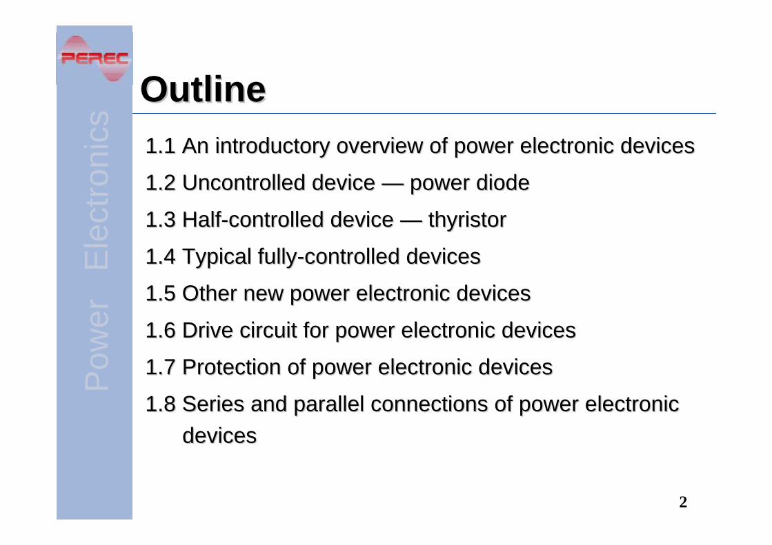
OutlineOutline1.1 An introductory overview of power electronic devices1.1 An introductory overview of power electronic devices
1.2 Uncontrolled device 1.2 Uncontrolled device —— power diodepower diode
1.3 Half1.3 Half--controlled device controlled device —— thyristorthyristor
1.4 Typical fully1.4 Typical fully--controlled devicescontrolled devices
1.5 Other new power electronic devices1.5 Other new power electronic devices
1.6 Drive circuit for power electronic devices1.6 Drive circuit for power electronic devices
1.7 Protection of power electronic devices1.7 Protection of power electronic devices
1.8 Series and parallel connections of power electronic 1.8 Series and parallel connections of power electronic devicesdevices

Pow
erE
l ect
roni
cs
3
The concept and featuresThe concept and features
Configuration of systems using power electronic devicesConfiguration of systems using power electronic devices
ClassificationsClassifications
Major topicsMajor topics
1.1 1.1 An introductory overview of power An introductory overview of power electronic deviceselectronic devices

Pow
erE
l ect
roni
cs
4
Power electronic devices:Power electronic devices:
In broad senseIn broad sense
Very often: Very often:
Major material used in power semiconductor devicesMajor material used in power semiconductor devices———— SiliconSilicon
are the electronic devices that can be directly used in the poweare the electronic devices that can be directly used in the power r processing circuits to convert or control electric power.processing circuits to convert or control electric power.
The concept of power electronic devicesThe concept of power electronic devices
power electronic devicespower electronic devices
Vacuum devices: Mercury arc Vacuum devices: Mercury arc rectifier rectifier thyratronthyratron, etc. . seldom , etc. . seldom in use todayin use today
Semiconductor devices: Semiconductor devices: major power electronic devicesmajor power electronic devices
Power electronic devices = Power semiconductor devicesPower electronic devices = Power semiconductor devices

Pow
erE
l ect
roni
cs
5
Features of power electronic devicesFeatures of power electronic devicesThe electric power that power electronic device The electric power that power electronic device deals with is usually much larger than that the deals with is usually much larger than that the information electronic device does.information electronic device does.
Usually working in switching states to reduce power Usually working in switching states to reduce power losseslosses
p=vi=0Off-state Current through the device is 0i=0
p=vi=0On-state Voltage across the device is 0v=0

Pow
erE
l ect
roni
cs
6
Features of power electronic devicesFeatures of power electronic devices
Need to be controlled by information electronic circuits.Need to be controlled by information electronic circuits.Very often, drive circuits are necessary to interface Very often, drive circuits are necessary to interface between information circuits and power circuits.between information circuits and power circuits.
Dissipated power loss usually larger than information Dissipated power loss usually larger than information electronic devices electronic devices —— special packaging and heat sink special packaging and heat sink are necessary.are necessary.

Pow
erE
l ect
roni
cs
7
Power losses on power semiconductor Power losses on power semiconductor devicesdevices
= conduction loss + turn= conduction loss + turn--off loss + offoff loss + off--state loss + turnstate loss + turn--on losson loss
O n - s ta te( c o n d u c t io n s ta te )
tu r n in g -o f f
O f f - s ta te( b lo c k in g s ta te )
tu r n in g- o n
t
t
t
v
i
p
Total power loss onTotal power loss onpower semiconductorpower semiconductor
Switching lossSwitching loss
(on(on--state loss)state loss)

Pow
erE
l ect
roni
cs
8
Configuration of systems using power Configuration of systems using power electronic deviceselectronic devices
Control circuit
detectioncircuit
drivecircuit
Power circuit(power stage,main circuit)
Control circuit (in a broad sense)
Power electronic system: Electric isolation:
optical, magnetic
Protection circuit is also very often used in power electronicsystem especially for the expensive power semiconductors.

Pow
erE
l ect
roni
cs
9
Terminals of a power electronic deviceTerminals of a power electronic device
C
E
G
A power electronic device must have at least two terminals to allow power circuit current flow through.
A power electronic device usually has a third terminal ——control terminal to control the states of the device.
Control signal from drive circuit must be connected between the Control signal from drive circuit must be connected between the control terminal and a fixed power circuit terminal (therefore control terminal and a fixed power circuit terminal (therefore
called common terminal ).called common terminal ).
Drive Circuit

Pow
erE
l ect
roni
cs
10
A classification of power electronic devicesA classification of power electronic devicesUncontrolled device: diodeUncontrolled device: diode(Uncontrollable device)(Uncontrollable device)
FullyFully--controlled device: Power MOSFET, IGBT,GTO, IGCTcontrolled device: Power MOSFET, IGBT,GTO, IGCT(Fully(Fully--controllable device)controllable device)
HalfHalf--controlled device:controlled device: thyristorthyristor(Half(Half--controllable device)controllable device)
has only two terminals and can not be controlled by control signal. The on and off states of the device are determined by the power circuit.
is turned-on by a control signal and turned-off by the power circuit
The on and off states of the device are controlled by control signals.

Pow
erE
l ect
roni
cs
11
Other classificationsOther classifications
power electronic devicespower electronic devicesPulsePulse--triggered devicestriggered devices
LevelLevel--sensitive (levelsensitive (level--triggered) devicestriggered) devices
power electronic devicespower electronic devices
power electronic devicespower electronic devicesCurrentCurrent--driven (currentdriven (current--controlled) devicescontrolled) devices
VoltageVoltage--driven (voltagedriven (voltage--controlled) devices controlled) devices (Field(Field--controlled devices)controlled devices)
UnipolarUnipolar devices (Majority carrier devices)devices (Majority carrier devices)
Composite devicesComposite devices
Bipolar devices (Minority carrier devices)Bipolar devices (Minority carrier devices)

Pow
erE
l ect
roni
cs
12
Appearance, structure, and symbol Appearance, structure, and symbol Physics of operationPhysics of operation
CharacteristicsCharacteristics
SpecificationSpecificationSpecial issuesSpecial issuesDevices of the same familyDevices of the same family
Major topics for each deviceMajor topics for each device
Switching characteristicsSwitching characteristics
Static characteristicsStatic characteristics

Pow
erE
l ect
roni
cs
13
Passive components in power electronic Passive components in power electronic circuitcircuit
Transformer, inductor, capacitor and resistor:Transformer, inductor, capacitor and resistor:these are passive components in a power electronic these are passive components in a power electronic
circuit since they can not be controlled by control signal and circuit since they can not be controlled by control signal and their characteristics are usually constant and linear.their characteristics are usually constant and linear.
The requirements for these passive components by power The requirements for these passive components by power electronic circuits could be very different from those by electronic circuits could be very different from those by ordinary circuits.ordinary circuits.
Pow
erE
l ect
roni
cs
14
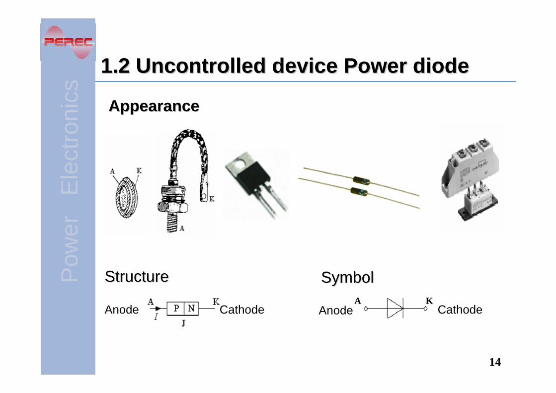
1.2 Uncontrolled device Power diode1.2 Uncontrolled device Power diode
AppearanceAppearance
StructureStructure SymbolSymbol
CathodeAnodeKKAA
Anode Cathode

Pow
erE
l ect
roni
cs
15
PN junctionPN junction
-。 -。 -。
-。 -。 -。
-。 -。 -。
-。 -。 -。
-。 -。 -。
+· +· +·
+· +· +·
+· +· +·
+·+· +
·
+· +· +·
+-
+-
+-
+-
+-
p region n region
Direction ofinner electric field
Space charge region
(depletion region,potential barrier
region)
Semiconductor (Column IV element, Semiconductor (Column IV element, SiSi))Electrons and holes.Electrons and holes.Pure semiconductor (intrinsic semiconductor)Pure semiconductor (intrinsic semiconductor)Doping, pDoping, p--type semiconductor. Ntype semiconductor. N--type semiconductortype semiconductorPN junctionPN junctionEquilibrium of diffusion and driftEquilibrium of diffusion and drift

Pow
erE
l ect
roni
cs
16
PN junction with voltage applied in the PN junction with voltage applied in the forward directionforward direction
V
+
+
+
+
+
--
-
-
-
np
Wo
W+ -

Pow
erE
l ect
roni
cs
17
PN junction with voltage applied in the reverse PN junction with voltage applied in the reverse directiondirection
+- V+
+
+
+
+
--
-
-
-
-
-
-
+
+
+
np
Wo
W
Effective directionof electronic field

Pow
erE
l ect
roni
cs
18
Construction of a practical power diodeConstruction of a practical power diode
Features different from lowFeatures different from low--power (information electronic) diodespower (information electronic) diodes–– Larger size–– Vertically oriented structure–– n drift region (p-i-n diode)–– Conductivity modulation
250μm
Breakdown voltage dependent
10 μmp
Nd =10 cmn substrate -319
Na =10 cm-319+
n epi Nd =10 cm -314
p
Nd =10 cmn substrate -319+
Na =10 cm-319+
n epi- Nd =10 cm -314
iAnode
Cathode
+
-
V
-
Pow
erE
l ect
roni
cs
19
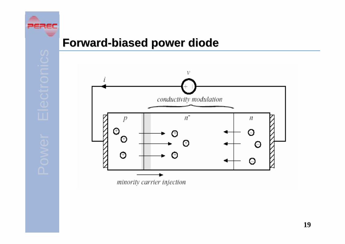
ForwardForward--biased power diodebiased power diode

Pow
erE
l ect
roni
cs
20
ReverseReverse--biased power diodebiased power diode
BreakdownBreakdown–– Avalanche breakdown–– Thermal breakdown

Pow
erE
l ect
roni
cs
21
The positive and negative charge in the depletion region is The positive and negative charge in the depletion region is variable with the changing of external voltage.variable with the changing of external voltage.——––Junction capacitor CJunction capacitor CJJ ..
Junction capacitor CJunction capacitor CJJ
Junction capacitor influences the switching characteristics of Junction capacitor influences the switching characteristics of power diode. power diode.
Junction capacitorJunction capacitor
Diffusion capacitor Diffusion capacitor CCDD
Potential barrier capacitor Potential barrier capacitor CCBB

Pow
erE
l ect
roni
cs
22
Static characteristics of power diodeStatic characteristics of power diode
The IThe I--V characteristic of power diode V characteristic of power diode
I
O
IF
UTO UF U
Pow
erE
l ect
roni
cs
23
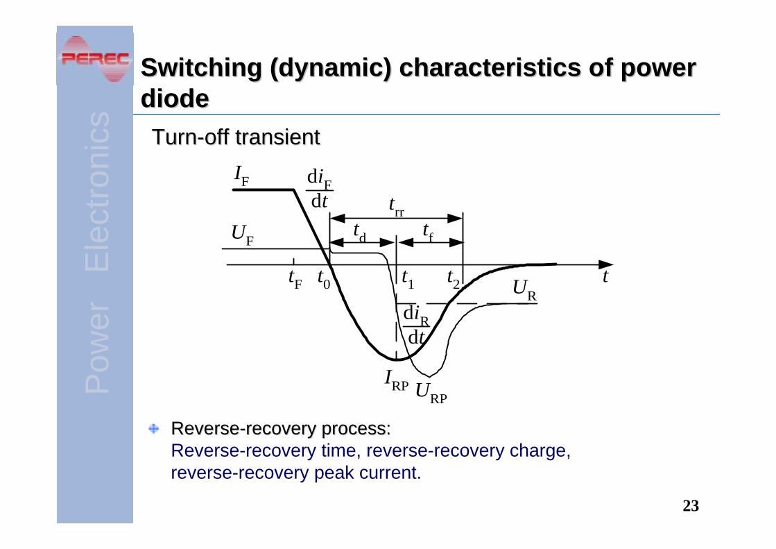
Switching (dynamic) characteristics of power Switching (dynamic) characteristics of power diodediode
ReverseReverse--recovery process:recovery process:Reverse-recovery time, reverse-recovery charge, reverse-recovery peak current.
TurnTurn--off transientoff transientIF
UF
tF t0
trrtd tf
t1 t2 tUR
URPIRP
diFdt
diRdt
Pow
erE
l ect
roni
cs
24
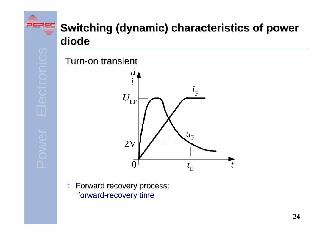
Switching (dynamic) characteristics Switching (dynamic) characteristics of power of power diodediode
Forward recovery process:Forward recovery process:forward-recovery time
TurnTurn--on transienton transient
UFP
ui
iF
uF
tfr t0
2V
Pow
erE
l ect
roni
cs
25
Specifications of power diodeSpecifications of power diode
Average rectified forward current IAverage rectified forward current IF(AV)F(AV)
Forward voltage UForward voltage UFF
Peak repetitive reverse voltage UPeak repetitive reverse voltage URRMRRM
Maximum junction temperature TMaximum junction temperature TJMJM
ReverseReverse--recovery time recovery time ttrrrr

Pow
erE
l ect
roni
cs
26
Types of power diodesTypes of power diodes
General purpose diode (rectifier diode):General purpose diode (rectifier diode):
Fast recovery diodeFast recovery diode
SchottkySchottky diode (diode (SchottkySchottky barrier diodebarrier diode--SBD)SBD)
standard recovery
Reverse recovery time and charge specified. trr is usually less than 1μs, for many less than 100 ns —— ultra-fast recovery diode.
– A majority carrier device– Essentially no recovered charge, and lower forward voltage.– Restricted to low voltage (less than 200V)

Pow
erE
l ect
roni
cs
27
Examples of commercial power diodesExamples of commercial power diodes

Pow
erE
l ect
roni
cs
28
History and applications of power diodeHistory and applications of power diode
Applied in industries starting 1950sApplied in industries starting 1950s
Still inStill in--use today. Usually working with controlled use today. Usually working with controlled devices as necessary componentsdevices as necessary components
In many circumstances fast recovery diodes or In many circumstances fast recovery diodes or schottkyschottky diodes have to be used instead of general diodes have to be used instead of general purpose diodes.purpose diodes.

Pow
erE
l ect
roni
cs
29
1.3 Half1.3 Half--controlled devicecontrolled device——ThyristorThyristor
Another name: SCRAnother name: SCR——silicon controlled rectifiersilicon controlled rectifier
ThyristorThyristor Opened the power electronics eraOpened the power electronics era–– 1956, invention, Bell Laboratories1956, invention, Bell Laboratories–– 1957, development of the 1st product, GE1957, development of the 1st product, GE–– 1958, 1st commercialized product, GE1958, 1st commercialized product, GE–– ThyristorThyristor replaced vacuum devices in almost every power replaced vacuum devices in almost every power
processing area.processing area.
Still in use in high power situation. Still in use in high power situation. ThyristorThyristor till has the till has the highest powerhighest power--handling capability. handling capability.
HistoryHistory

Pow
erE
l ect
roni
cs
30
Appearance and symbol of Appearance and symbol of thyristorthyristor
SymbolSymbolAppearanceAppearance
KG
A
CathodeCathode
AnodeAnodeGateGate
Pow
erE
l ect
roni
cs
31
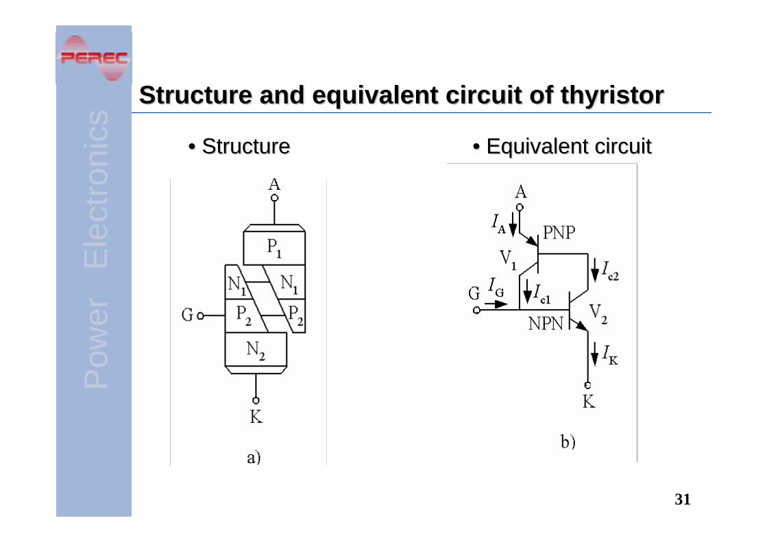
Structure and equivalent circuit of Structure and equivalent circuit of thyristorthyristor
•• StructureStructure •• Equivalent circuitEquivalent circuit
Pow
erE
l ect
roni
cs
32
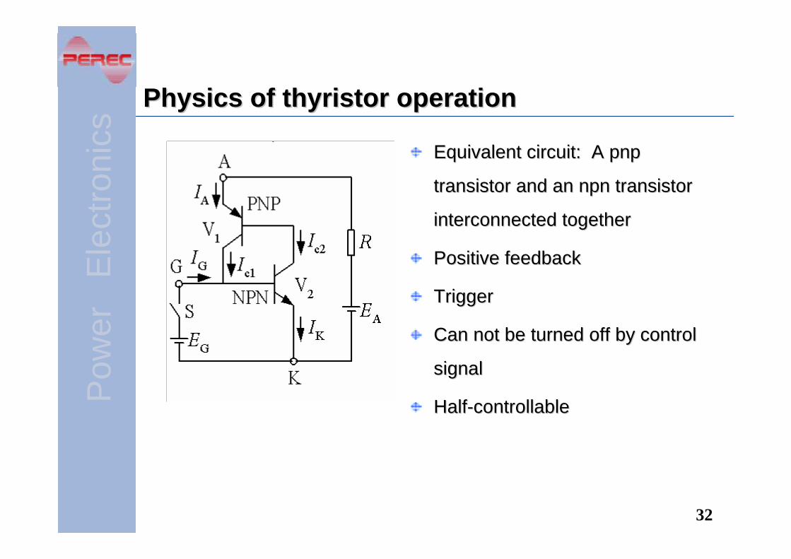
Physics of Physics of thyristorthyristor operationoperation
Equivalent circuit: A Equivalent circuit: A pnppnp
transistor and an transistor and an npnnpn transistor transistor
interconnected togetherinterconnected together
Positive feedbackPositive feedback
TriggerTrigger
Can not be turned off by control Can not be turned off by control
signalsignal
HalfHalf--controllablecontrollable

Pow
erE
l ect
roni
cs
33
Quantitative description of Quantitative description of thyristorthyristor operationoperation
IIc1c1==αα11 IIAA ++ IICBO1CBO1 ((11--11))
IIc2c2==αα22 IIKK ++ IICBO2CBO2 ((11--22))
IIKK==IIAA++IIG G ((11--33))
IIAA==IIcc11++IIcc2 2 ((11--44))
)(1 21
CBO2CBO1G2A αα
α+−
++=
IIII ((11--55))
When IWhen IGG=0, =0, αα11+α+α22 is small.is small.When IWhen IGG>0, >0, αα11+α+α22 will approach 1, Iwill approach 1, IAA will be very large.will be very large.

Pow
erE
l ect
roni
cs
34
Other methods to trigger Other methods to trigger thyristorthyristor onon
High voltage across anode and cathodeHigh voltage across anode and cathode——avalanche breakdownavalanche breakdown
High rising rate of anode High rising rate of anode voltagtevoltagte —— du/dtdu/dt too hightoo high
High junction temperatureHigh junction temperature
Light activationLight activation

Pow
erE
l ect
roni
cs
35
Static characteristics of Static characteristics of thyristorthyristor
Blocking when reverse Blocking when reverse biased, no matter if there biased, no matter if there is gate current appliedis gate current appliedConducting only when Conducting only when forward biased and there forward biased and there is triggering current is triggering current applied to the gateapplied to the gateOnce triggered on, will be Once triggered on, will be latched on conducting latched on conducting even when the gate even when the gate current is no longer current is no longer applied applied Turning off: decreasing Turning off: decreasing current to be near zero current to be near zero with the effect of external with the effect of external power circuitpower circuitGate IGate I--V characteristicsV characteristics
O UAk
IA
IH
IG2
IG1
IG=0
Ubo
UDSM
UDRM
URRM
URSM
forward forward conductingconducting
avalanche avalanche breakdownbreakdown
reverse reverse blockingblocking
increasing IG
forward forward blockingblocking

Pow
erE
l ect
roni
cs
36
Switching characteristics of Switching characteristics of thyristorthyristor
TurnTurn--on transienton transient–– Delay time tDelay time tdd
–– Rise time Rise time ttrr
–– TurnTurn--on time on time ttgtgt
TurnTurn--off transient off transient –– Reverse recovery Reverse recovery
time time ttrrrr
–– Forward recovery Forward recovery time time ttgrgr
–– TurnTurn--off time off time ttqq
100%90%
10%
uAK
t
tO
0 td tr
trr tgrURRM
IRM
iA
Pow
erE
l ect
roni
cs
37
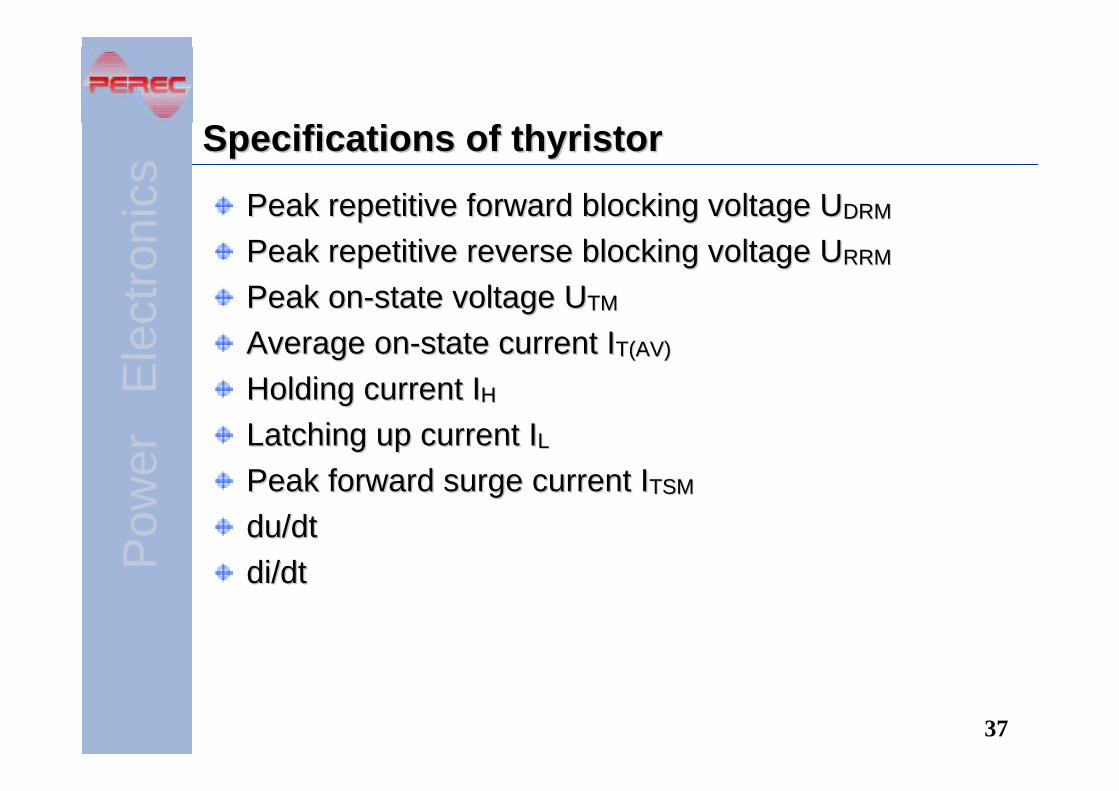
Specifications of Specifications of thyristorthyristor
Peak repetitive forward blocking voltage UPeak repetitive forward blocking voltage UDRMDRM
Peak repetitive reverse blocking voltage UPeak repetitive reverse blocking voltage URRMRRM
Peak onPeak on--state voltage Ustate voltage UTMTM
Average onAverage on--state current Istate current IT(AV)T(AV)
Holding current IHolding current IHH
Latching up current ILatching up current ILL
Peak forward surge current IPeak forward surge current ITSMTSM
du/dtdu/dtdi/dtdi/dt

Pow
erE
l ect
roni
cs
38
The family of The family of thyristorsthyristorsFast switching Fast switching thyristorthyristor——FSTFSTTriode AC switchTriode AC switch——TRIAC TRIAC (Bi(Bi--directional triode directional triode thyristorthyristor))
ReverseReverse--conductingconducting thyristor thyristor LightLight--triggered (triggered (activitedactivited)) thyristorthyristor——RCT RCT ——LTTLTT
I
O U
IG=0
KG
A
A
G
K
G
K
A
G
T1
T2

Pow
erE
l ect
roni
cs
39
1.4 Typical fully1.4 Typical fully--controlled devicescontrolled devices1.4.1 Gate1.4.1 Gate--turnturn--off off thyristorthyristor ——GTOGTO1.4.2 Giant transistor 1.4.2 Giant transistor ——GTRGTR1.4.3 Power metal1.4.3 Power metal--oxideoxide--semiconductor field effect semiconductor field effect
transistor transistor —— Power MOSFETPower MOSFET1.4.4 Insulated1.4.4 Insulated--gate bipolar transistor gate bipolar transistor ——IGBTIGBT
FeaturesFeatures
–– Begin to be used in large amount in 1980sBegin to be used in large amount in 1980s–– GTR is obsolete and GTO is also seldom used today. GTR is obsolete and GTO is also seldom used today. –– IGBT and power MOSFET are the two major power IGBT and power MOSFET are the two major power
semiconductor devices nowadays. semiconductor devices nowadays.
ApplicationsApplications
–– IC fabrication technology, fullyIC fabrication technology, fully--controllable, high frequencycontrollable, high frequency
Pow
erE
l ect
roni
cs
40
A
G K G GK
N1
P1
N2N2 P2
b)a)
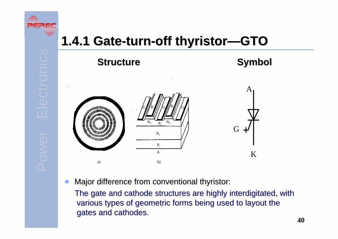
1.4.1 Gate1.4.1 Gate--turnturn--off off thyristorthyristor——GTOGTO
Major difference from conventional Major difference from conventional thyristorthyristor::The gate and cathode structures are highly The gate and cathode structures are highly interdigitatedinterdigitated, with , with various types of geometric forms being used to layout the various types of geometric forms being used to layout the gates and cathodes.gates and cathodes.
StructureStructure SymbolSymbol
G
K
A

Pow
erE
l ect
roni
cs
41
Physics of GTO operationPhysics of GTO operationThe basic operation of GTO is the The basic operation of GTO is the same as that of the conventional same as that of the conventional thyristorthyristor. .
The principal differences lie in the The principal differences lie in the modifications in the structure to modifications in the structure to achieve gate turnachieve gate turn--off capability. off capability. –– Large Large αα22
–– αα11++αα22 is just a little larger than is just a little larger than the critical value 1. the critical value 1.
–– Short distance from gate to Short distance from gate to cathode makes it possible to cathode makes it possible to drive current out of gate.drive current out of gate.
R
NPN
PNP
A
G
S
K
EG
IG
EAIK
Ic2Ic1
IA
V1
V2

Pow
erE
l ect
roni
cs
42
Characteristics of GTOCharacteristics of GTOStatic characteristicStatic characteristic–– Identical to conventional Identical to conventional thyristorthyristor in the forward directionin the forward direction–– Rather low reverse breakdown voltage (20Rather low reverse breakdown voltage (20--30V)30V)
Switching characteristicSwitching characteristic
O t
0 t
iG
iAIA
90%IA
10%IA
tttftstd tr
t0 t1 t2 t3 t4 t5 t6

Pow
erE
l ect
roni
cs
43
Specifications of GTOSpecifications of GTO
Most GTO specifications have the same meanings Most GTO specifications have the same meanings as those of conventional as those of conventional thyristorthyristor..
Specifications different from Specifications different from thyristorthyristor’’ss–– Maximum controllable anode current IMaximum controllable anode current IATOATO
–– Current turnCurrent turn--off gain off gain ββoffoff
–– TurnTurn--on time ton time tonon
–– TurnTurn--off time off time ttoffoff

Pow
erE
l ect
roni
cs
44
1.4.2 Giant Transistor1.4.2 Giant Transistor——GTRGTRGTR is actually the bipolar junction transistor that can handle GTR is actually the bipolar junction transistor that can handle high voltage and large current. high voltage and large current. So GTR is also called power BJT, or just BJT.So GTR is also called power BJT, or just BJT.
Basic structureBasic structure SymbolSymbol
b
e
c

Pow
erE
l ect
roni
cs
45
Structures of GTR different from its Structures of GTR different from its informationinformation--processing counterpartprocessing counterpart
MultipleMultiple--emitter structureemitter structure Darlington configurationDarlington configuration

Pow
erE
l ect
roni
cs
46
Physics of GTR operationPhysics of GTR operation
Same as information BJT deviceSame as information BJT device
holes
electronsEb
Ec
ib
ic=βib
ie=(1+β )ib

Pow
erE
l ect
roni
cs
47
Static characteristics of GTRStatic characteristics of GTR
cut-off region
Amplifying (active) region
O
I
ib3
ib2
ib1ib1<ib2<ib3
Uce
Satu
ratio
n re
gion

Pow
erE
l ect
roni
cs
48
Switching characteristics of GTRSwitching characteristics of GTR
TurnTurn--on transienton transient–– TurnTurn--on delay time ton delay time tdd
–– Rise time Rise time ttrr
–– TurnTurn--on time ton time tonon
TurnTurn--off transientoff transient–– Storage time Storage time ttss
–– Falling time Falling time ttff
–– TurnTurn--off timeoff time ttoffoff
ib Ib
1
Ib
2
Icsic
0
0
90%Ib1
10%Ib1
90%Ics
10%Ics
t0 t1 t2 t3 t4 t5 t
t
toffts tf
ton
trtd

Pow
erE
l ect
roni
cs
49
Second breakdown of GTRSecond breakdown of GTR

Pow
erE
l ect
roni
cs
50
Safe operating area (SOA) of GTRSafe operating area (SOA) of GTR
S O A
O
I c
I c MP S B
P c M
U c eU c e M

Pow
erE
l ect
roni
cs
51
1.4.3 Power metal1.4.3 Power metal--oxideoxide--semiconductor field semiconductor field effect transistoreffect transistor——Power MOSFETPower MOSFET
Basic structureBasic structure SymbolSymbol
G
S
D
P channel
A classification A classification
Field Effect Field Effect TransistorTransistor(FET)(FET)
MetalMetal--onsideonside--semiconductor FET (MOSFET)semiconductor FET (MOSFET) Power MOSFETPower MOSFET
Junction FET (JFET)Junction FET (JFET) Static induction transistor (SIT)Static induction transistor (SIT)
n channeln channelp channelp channel
G
S
D
N channel
Pow
erE
l ect
roni
cs
52
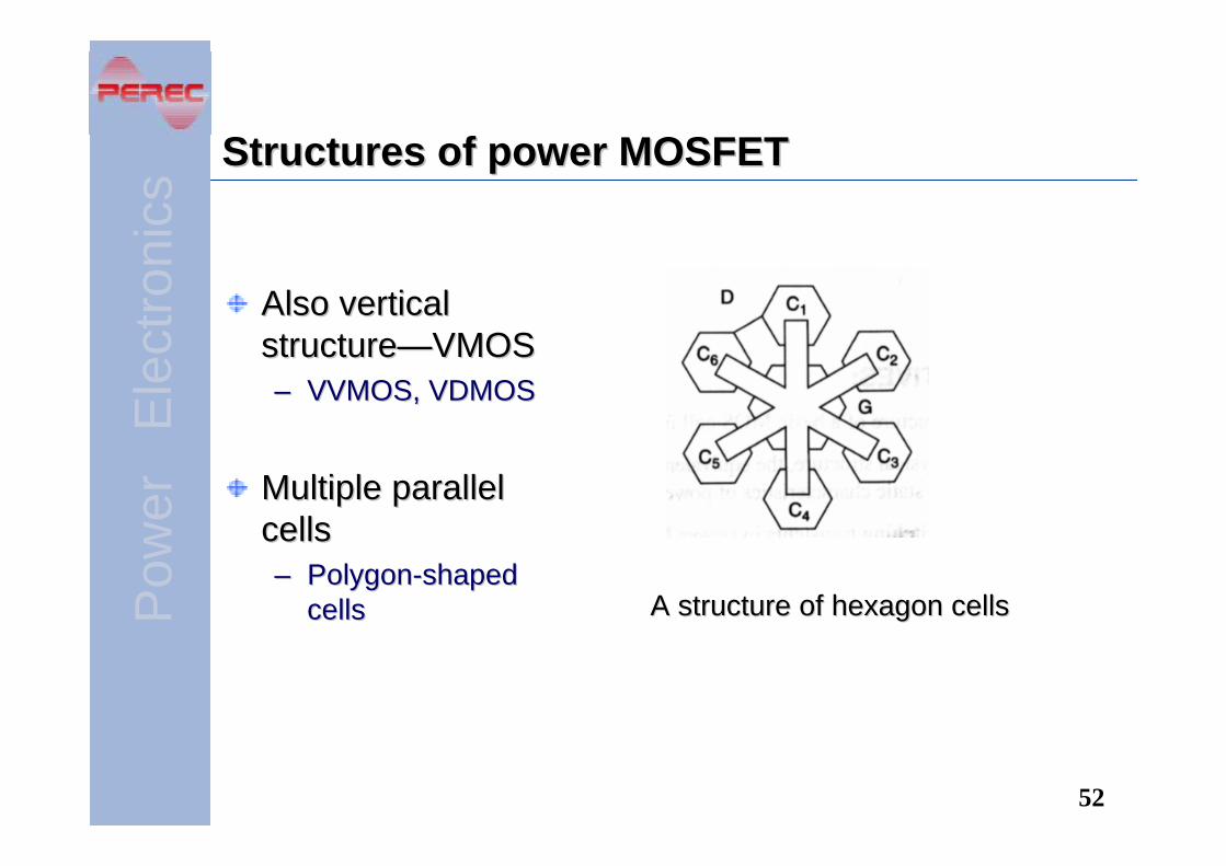
Structures of power MOSFETStructures of power MOSFET
Also vertical Also vertical structurestructure——VMOSVMOS–– VVMOS, VDMOSVVMOS, VDMOS
Multiple parallel Multiple parallel cellscells–– PolygonPolygon--shaped shaped
cellscells A structure of hexagon cellsA structure of hexagon cells
Pow
erE
l ect
roni
cs
53
Physics of MOSFET operationPhysics of MOSFET operation
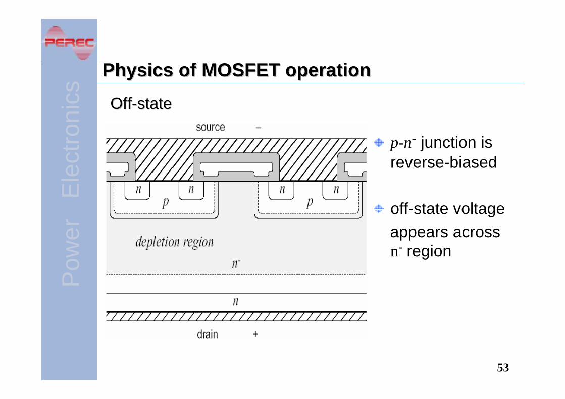
p-n- junction is reverse-biased
off-state voltageappears across n- region
OffOff--statestate

Pow
erE
l ect
roni
cs
54
Physics of MOSFET operationPhysics of MOSFET operation
p-n- junction is slightly reverse biasedpositive gate voltage induces conducting channeldrain current flows through n- region and conducting channelon resistance = total resistances of n- region, conducting channel,source and drain contacts, etc.
OnOn--statestate
Pow
erE
l ect
roni
cs
55
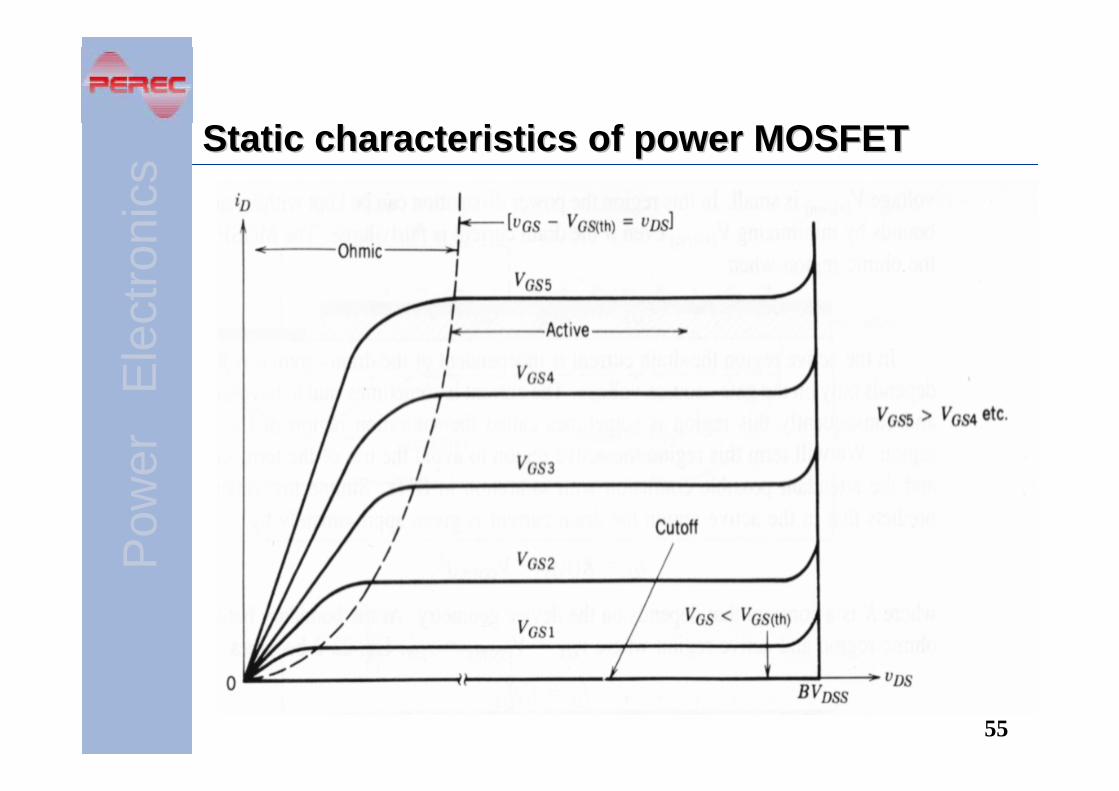
Static characteristics of power MOSFETStatic characteristics of power MOSFET

Pow
erE
l ect
roni
cs
56
Switching characteristics of power MOSFETSwitching characteristics of power MOSFET
RsRG RF
RL
iD
uGSup
iD
+UE
iDO
O
O
up
t
t
t
uGSuGSPuT
td(on) trtd(off) tf
TurnTurn--on transienton transient–– TurnTurn--on delay time ton delay time td(on)d(on)
–– Rise time Rise time ttrr
TurnTurn--off transientoff transient
–– TurnTurn--off delay time toff delay time td(off)d(off)
–– Falling time Falling time ttff

Pow
erE
l ect
roni
cs
57
Specifications of power MOSFETSpecifications of power MOSFET
DrainDrain--source breakdown voltage Usource breakdown voltage UDSDS
Continuous drain current IContinuous drain current IDD
Peak pulsed drain current IPeak pulsed drain current IDMDM
On (OnOn (On--state) resistance Rstate) resistance RDS(on)DS(on)
InterInter--terminal capacitancesterminal capacitances–– Short circuit input capacitance Short circuit input capacitance CCississ== CCGSGS++ CCGDGD
–– Reverse transfer capacitance Reverse transfer capacitance CCrssrss== CCGDGD
–– Short circuit output capacitance Short circuit output capacitance CCossoss== CCDSDS++ CCGDGD
SOA of power MOSFETSOA of power MOSFET–– No second breakdownNo second breakdown

Pow
erE
l ect
roni
cs
58
Examples of commercial power MOSFETExamples of commercial power MOSFET

Pow
erE
l ect
roni
cs
59
Features and applications of power MOSFETFeatures and applications of power MOSFET
VoltageVoltage--driven device, simple drive circuitdriven device, simple drive circuitMajorityMajority--carrier device, fast switching speed, high carrier device, fast switching speed, high operating frequency (could be hundreds of kHz)operating frequency (could be hundreds of kHz)MajorityMajority--carrier device, better thermal stabilitycarrier device, better thermal stabilityOnOn--resistance increases rapidly with rated blocking resistance increases rapidly with rated blocking voltagevoltage–– Usually used at voltages less than 500V and power less Usually used at voltages less than 500V and power less
than 10kWthan 10kW–– 1000V devices are available, but are useful only at low 1000V devices are available, but are useful only at low
power levels(100W)power levels(100W)
Part number is selected on the basis of onPart number is selected on the basis of on--resistance rather than current ratingresistance rather than current rating

Pow
erE
l ect
roni
cs
60
The body diode of power MOSFETThe body diode of power MOSFET
The body diodeThe body diode Equivalent circuitEquivalent circuit
Pow
erE
l ect
roni
cs
61
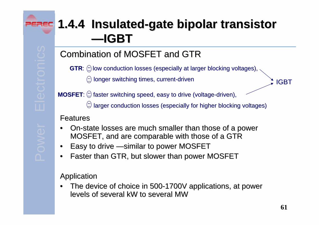
1.4.4 1.4.4 InsulatedInsulated--gate bipolar transistor gate bipolar transistor ——IGBTIGBT
FeaturesFeatures•• OnOn--state losses are much smaller than those of a power state losses are much smaller than those of a power
MOSFET, and are comparable with those of a GTRMOSFET, and are comparable with those of a GTR•• Easy to drive Easy to drive ——similar to power MOSFETsimilar to power MOSFET•• Faster than GTR, but slower than power MOSFETFaster than GTR, but slower than power MOSFET
ApplicationApplication•• The device of choice in 500The device of choice in 500--1700V applications, at power 1700V applications, at power
levels of several kW to several MWlevels of several kW to several MW
Combination of MOSFET and GTRCombination of MOSFET and GTRGTRGTR: low conduction losses (especially at larger blocking volta: low conduction losses (especially at larger blocking voltages),ges),
longer switching times, currentlonger switching times, current--drivendriven
MOSFETMOSFET: faster switching speed, easy to drive (voltage: faster switching speed, easy to drive (voltage--driven),driven),
larger conduction losses (especially for hilarger conduction losses (especially for higher blocking voltages)gher blocking voltages)
IGBTIGBT

Pow
erE
l ect
roni
cs
62
Structure and operation principle of IGBTStructure and operation principle of IGBT
Basic structureBasic structure Also multiple cell structureAlso multiple cell structureBasic structure similar to Basic structure similar to power MOSFET, except power MOSFET, except extra p regionextra p regionOnOn--state: minority carriers state: minority carriers are injected into drift region, are injected into drift region, leading to conductivity leading to conductivity modulationmodulationcompared with power compared with power MOSFET: slower switching MOSFET: slower switching times, lower ontimes, lower on--resistance, resistance, useful at higher voltages useful at higher voltages (up to 1700V)(up to 1700V)
E G
C
N+N-
a)
PN+ N+PN+ N+
P+
Emitter Gate
Collector
Injecting layerBuffer layerDrift regionJ3 J2
J1

Pow
erE
l ect
roni
cs
63
Equivalent circuit and circuit symbol of IGBTEquivalent circuit and circuit symbol of IGBT
Equivalent circuitEquivalent circuit Circuit symbolCircuit symbol
G
E
C
+
-
+-
+
-
ID RN
IC
VJ1
IDRon
Drift regionresistance
G
C
E
Pow
erE
l ect
roni
cs
64
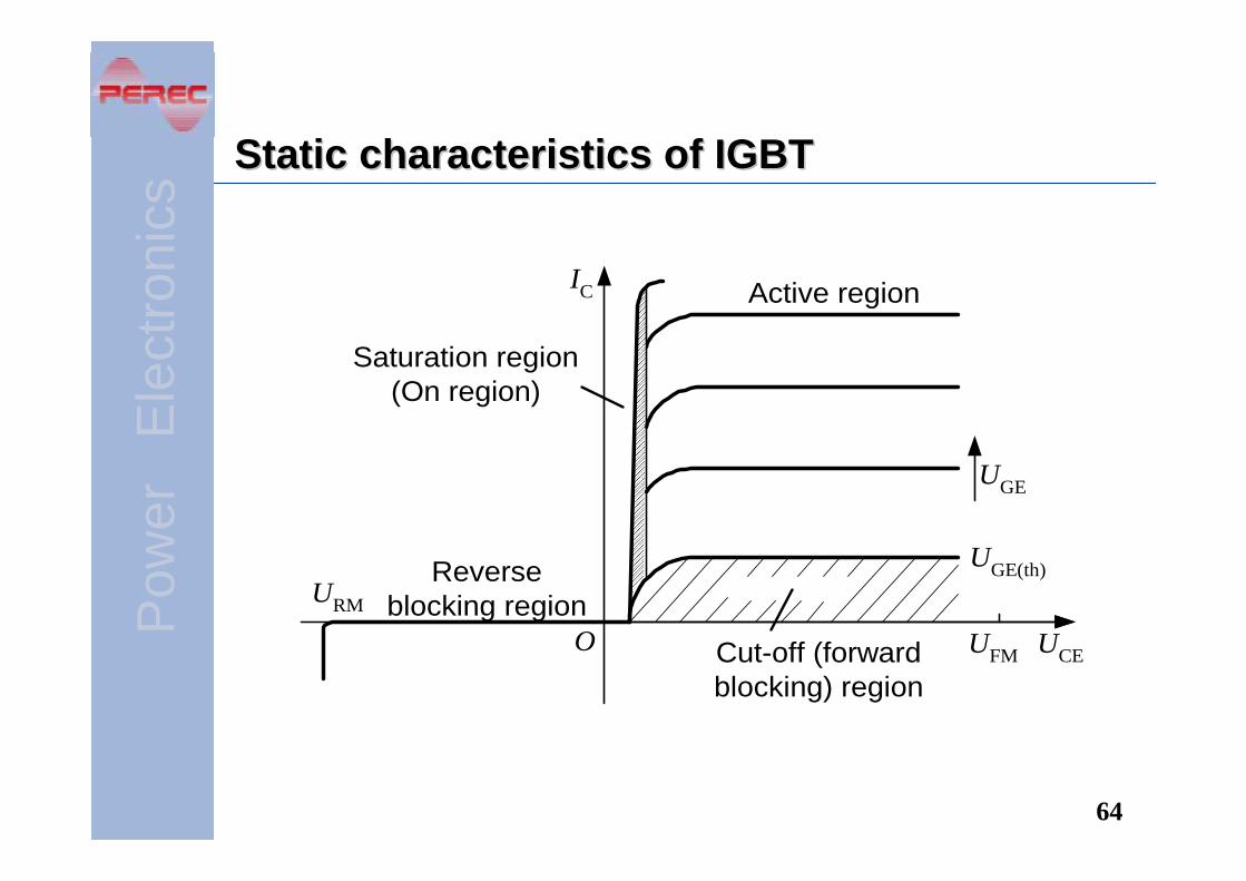
Static characteristics of IGBTStatic characteristics of IGBT
O
Active region
Cut-off (forwardblocking) region
Saturation region(On region)
Reverseblocking region
IC
URM
UFM UCE
UGE(th)
UGE

Pow
erE
l ect
roni
cs
65
Switching characteristics of IGBTSwitching characteristics of IGBT
IGBT turn-on is similar to power MOSFET turn-on
The major difference between IGBT turn-off and power MOSFET turn-off:– There is current
tailing in the IGBT turn-off due to the stored charge in the drift region.
t
t
t
10%
90%
10%
90%
UCE
IC
0
O
0
UGE UGEM
ICM
UCEM
tfv1 tfv2
toffton
tfi1 tfi2
td(off) tftd(on) tr
UCE(on)
UGEM
UGEM
ICM
ICMcurrent tail
Pow
erE
l ect
roni
cs
66
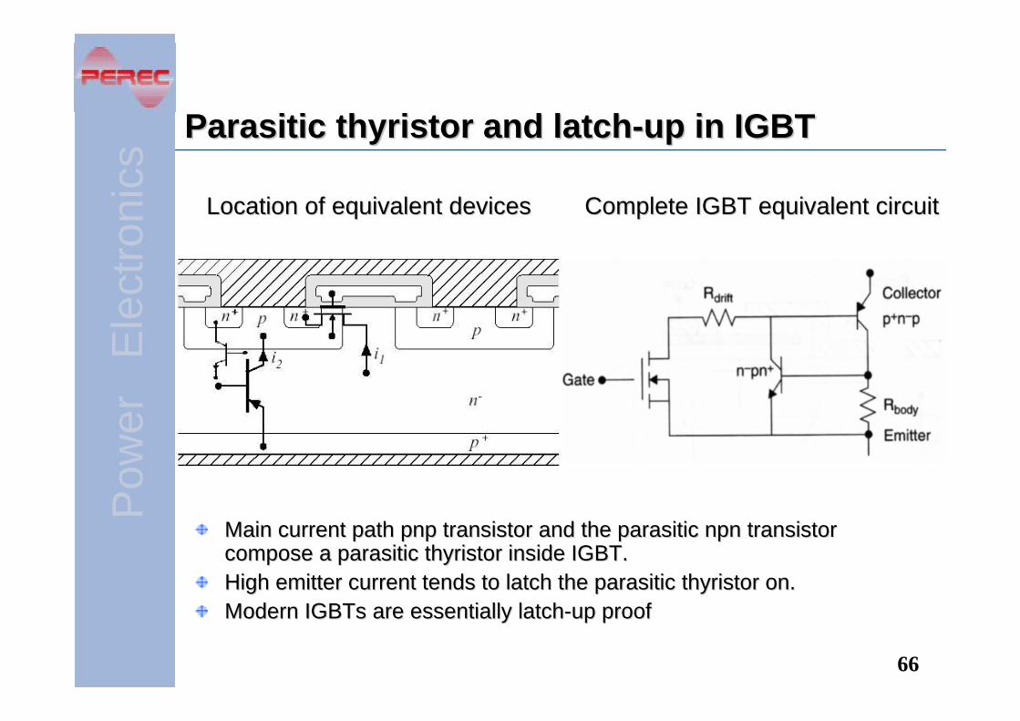
Parasitic Parasitic thyristorthyristor and latchand latch--up in IGBTup in IGBT
Main current path Main current path pnppnp transistor and the parasitic transistor and the parasitic npnnpn transistor transistor compose a parasitic compose a parasitic thyristorthyristor inside IGBT.inside IGBT.High emitter current tends to latch the parasitic High emitter current tends to latch the parasitic thyristorthyristor on.on.Modern Modern IGBTsIGBTs are essentially latchare essentially latch--up proofup proof
Location of equivalent devicesLocation of equivalent devices Complete IGBT equivalent circuitComplete IGBT equivalent circuit

Pow
erE
l ect
roni
cs
67
Specifications of IGBTSpecifications of IGBT
CollectorCollector--emitter breakdown voltage Uemitter breakdown voltage UCESCES
Continuous collector current IContinuous collector current ICC
Peak pulsed collector current IPeak pulsed collector current ICMCM
Maximum power dissipation PMaximum power dissipation PCMCM
Other issues:Other issues:SOA of IGBTSOA of IGBT–– The IGBT has a rectangular SOA with similar shape to the The IGBT has a rectangular SOA with similar shape to the
power MOSFET.power MOSFET.
Usually fabricated with an antiUsually fabricated with an anti--parallel fast diodeparallel fast diode

Pow
erE
l ect
roni
cs
68
Examples of commercial IGBTExamples of commercial IGBT

Pow
erE
l ect
roni
cs
69
1.5 Other new power electronic devices1.5 Other new power electronic devicesStatic induction transistor Static induction transistor ——SITSIT
Static induction Static induction thyristorthyristor ——SITHSITH
MOS controlled MOS controlled thyristorthyristor —— MCTMCT
Integrated gateIntegrated gate--commutated commutated thyristorthyristor ——IGCTIGCT
Power integrated circuit and power modulePower integrated circuit and power module

Pow
erE
l ect
roni
cs
70
Static induction transistorStatic induction transistor——SITSIT
Another name: power junction field effect Another name: power junction field effect transistortransistor——power JFETpower JFET
FeaturesFeatures–– MajorMajor--carrier devicecarrier device–– Fast switching, comparable to power MOSFETFast switching, comparable to power MOSFET–– Higher powerHigher power--handling capability than power MOSFEThandling capability than power MOSFET–– Higher conduction losses than power MOSFETHigher conduction losses than power MOSFET–– NormallyNormally--on device, not convenient (could be made on device, not convenient (could be made
normallynormally--off, but with even higher onoff, but with even higher on--state losses)state losses)

Pow
erE
l ect
roni
cs
71
Static induction Static induction thyristorthyristor——SITHSITH
other namesother names–– Field controlled Field controlled thyristorthyristor——FCTFCT–– Field controlled diodeField controlled diode
FeaturesFeatures–– MinorityMinority--carrier device, a JFET structure with an additional carrier device, a JFET structure with an additional
injecting layerinjecting layer–– PowerPower--handling capability similar to GTOhandling capability similar to GTO–– Faster switching speeds than GTOFaster switching speeds than GTO–– NormallyNormally--on device, not convenient (could be made on device, not convenient (could be made
normallynormally--off, but with even higher onoff, but with even higher on--state losses)state losses)
Pow
erE
l ect
roni
cs
72
MOS controlled MOS controlled thyristorthyristor——MCTMCT
Essentially a GTO with integrated MOSEssentially a GTO with integrated MOS--driven driven gates controlling both turngates controlling both turn--on and turnon and turn--off that off that potentially will significantly simply the design of potentially will significantly simply the design of circuits using GTO.circuits using GTO.
The difficulty is how to design a MCT that can be The difficulty is how to design a MCT that can be turned on and turned off equally well. turned on and turned off equally well.
Once believed as the most promising device, but Once believed as the most promising device, but still not commercialized in a large scale. The future still not commercialized in a large scale. The future remains uncertain. remains uncertain.

Pow
erE
l ect
roni
cs
73
Integrated gateIntegrated gate--commutated commutated thyristorthyristor —— IGCTIGCT
The newest member of the power semiconductor The newest member of the power semiconductor family, introduced in 1997 by ABBfamily, introduced in 1997 by ABBActually the close integration of GTO and the gate Actually the close integration of GTO and the gate drive circuit with multiple drive circuit with multiple MOSFETsMOSFETs in parallel in parallel providing the gate currentsproviding the gate currentsShort name: GCTShort name: GCTConduction drop, gate driver loss, and switching Conduction drop, gate driver loss, and switching speed are superior to GTOspeed are superior to GTOCompeting with IGBT and other new devices to Competing with IGBT and other new devices to replace GTO replace GTO
Pow
erE
l ect
roni
cs
74
Power integrated circuit and power modulePower integrated circuit and power module
Two major challengesTwo major challenges–– Electrical isolation of highElectrical isolation of high--voltage components from lowvoltage components from low--
voltage componentsvoltage components–– Thermal managementThermal management——power devices usually at higher power devices usually at higher
temperatures than lowtemperatures than low--voltage devicesvoltage devices
Integration of power electronic devices
Monolithic integration:Monolithic integration:power integrated circuitpower integrated circuit
Packaging integration: Packaging integration: power modulepower module
Smart power integrated circuit(Smart power IC, SPIC, Smart switch)
High voltage integrated circuit (HVIC)
Ordinary power module:just power devices packaged together
Integrated power electronics Module(IPEM): power devices, drive circuit, protection circuit, control circuit
Intelligent power module (IPM):power devices, drive circuit, protection circuit

Pow
erE
l ect
roni
cs
75
Review of device classificationsReview of device classifications
power electronicpower electronicdevicesdevices
PulsePulse--triggered devices: triggered devices: thyristorthyristor, GTO , GTO
LevelLevel--sensitive (Levelsensitive (Level--triggered) devices: triggered) devices: GTR,power MOSFET, IGBT, SIT, SITH, GTR,power MOSFET, IGBT, SIT, SITH, MCT, IGCTMCT, IGCT
power electronicpower electronicdevicesdevices
power electronicpower electronicdevicesdevices
CurrentCurrent--driven (currentdriven (current--controlled) devices:controlled) devices:thyristor, GTO, GTRVoltageVoltage--driven (voltagedriven (voltage--controlled) devices controlled) devices (Field(Field--controlled devices):power MOSFET, controlled devices):power MOSFET, IGBT, SIT, SITH, MCT, IGCTIGBT, SIT, SITH, MCT, IGCT
UniUni--polar devices (Majority carrier devices): polar devices (Majority carrier devices): SBD, power MOSFET, SITSBD, power MOSFET, SIT
Composite devices: IGBT, SITH, MCTComposite devices: IGBT, SITH, MCT
Bipolar devices (MinorityBipolar devices (Minority carrier devices): carrier devices): ordinary power diode, ordinary power diode, thyristorthyristor, GTO, GTR, , GTO, GTR, IGCT, IGBT, SITH, MCTIGCT, IGBT, SITH, MCT

Pow
erE
l ect
roni
cs
76
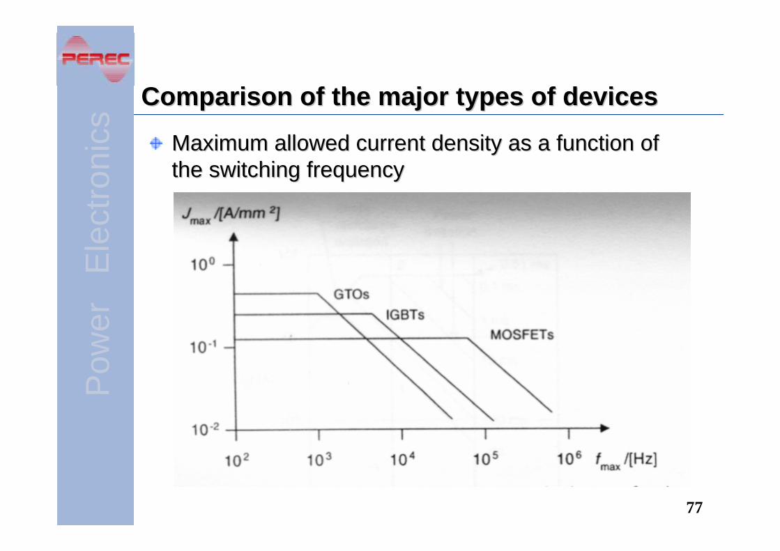
Comparison of the major types of devicesComparison of the major types of devices
PowerPower--handling capabilityhandling capability
Pow
erE
l ect
roni
cs
77
Comparison of the major types of devicesComparison of the major types of devices
Maximum allowed current density as a function of Maximum allowed current density as a function of the switching frequencythe switching frequency
Related Documents