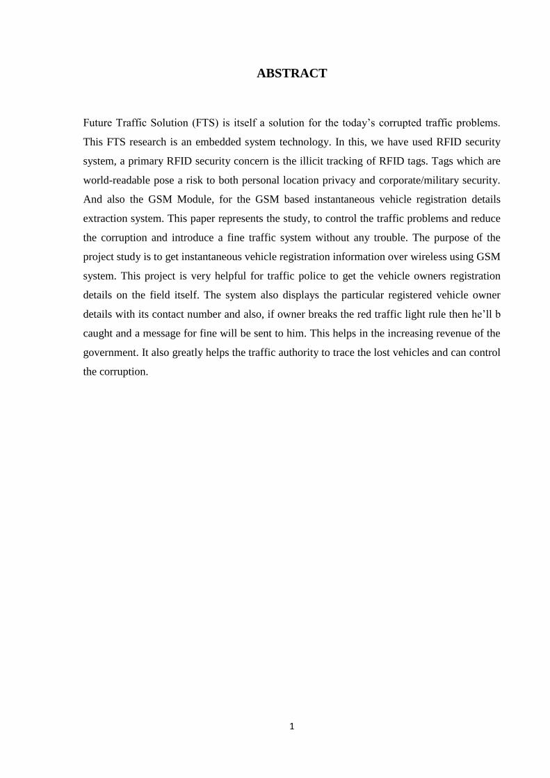
1 ABSTRACT Future Traffic Solution (FTS) is itself a solution for the today’s corrupted traffic problems. This FTS research is an embedded system technology. In this, we have used RFID security system, a primary RFID security concern is the illicit tracking of RFID tags. Tags which are world-readable pose a risk to both personal location privacy and corporate/military security. And also the GSM Module, for the GSM based instantaneous vehicle registration details extraction system. This paper represents the study, to control the traffic problems and reduce the corruption and introduce a fine traffic system without any trouble. The purpose of the project study is to get instantaneous vehicle registration information over wireless using GSM system. This project is very helpful for traffic police to get the vehicle owners registration details on the field itself. The system also displays the particular registered vehicle owner details with its contact number and also, if owner breaks the red traffic light rule then he’ll b caught and a message for fine will be sent to him. This helps in the increasing revenue of the government. It also greatly helps the traffic authority to trace the lost vehicles and can control the corruption.

Welcome message from author
This document is posted to help you gain knowledge. Please leave a comment to let me know what you think about it! Share it to your friends and learn new things together.
Transcript
1
ABSTRACT
Future Traffic Solution (FTS) is itself a solution for the today’s corrupted traffic problems.
This FTS research is an embedded system technology. In this, we have used RFID security
system, a primary RFID security concern is the illicit tracking of RFID tags. Tags which are
world-readable pose a risk to both personal location privacy and corporate/military security.
And also the GSM Module, for the GSM based instantaneous vehicle registration details
extraction system. This paper represents the study, to control the traffic problems and reduce
the corruption and introduce a fine traffic system without any trouble. The purpose of the
project study is to get instantaneous vehicle registration information over wireless using GSM
system. This project is very helpful for traffic police to get the vehicle owners registration
details on the field itself. The system also displays the particular registered vehicle owner
details with its contact number and also, if owner breaks the red traffic light rule then he’ll b
caught and a message for fine will be sent to him. This helps in the increasing revenue of the
government. It also greatly helps the traffic authority to trace the lost vehicles and can control
the corruption.

2
Chapter 1
INTRODUCTION
Traffic lights, also known as traffic signals, traffic lamps, signal lights, stop
lights and robots, and also known technically as traffic control signals are signalling devices
positioned at road intersections, pedestrian crossings and other locations to control competing
flows of traffic. Traffic lights were first installed in 1868 in London and are now used all over
the world. Traffic lights alternate the right of way accorded to road users by displaying lights
of a standard colour (red, yellow, and green) following a universal colour code. In the typical
sequence of colour phases:
The green light allows traffic to proceed in the direction denoted, if it is safe to do so.
The yellow light denoting prepare to stop short of the intersection, if it is safe to do so.
The red signal prohibits any traffic from proceeding.
1.1 HISTORY:
On 10 December 1868, the first traffic lights were installed outside the British Houses of
Parliament in London to control the traffic in Bridge Street, Great George Street and
Parliament Street. They were promoted by the railway engineer J. P. Knight and constructed
by the railway signal engineers of Saxby & Farmer. The design combined
three semaphore arms with red and green gas lamps for night-time use, on a pillar, operated
by a police constable. The gas lantern was turned with a lever at its base so that the
appropriate light faced traffic. Although it was said to be successful at controlling traffic, its
operational life was brief. It exploded on 2 January 1869, as a result of a leak in one of the
gas lines underneath the pavement, injuring or killing the policeman who was operating it.
With doubts about its safety, the concept was abandoned until electric signals became
available. The first electric traffic light was developed in 1912 by Lester Wire, an American
policeman of Salt Lake City, Utah, who also used red-green lights. On 5 August 1914,
the American Traffic Signal Company installed a traffic signal system on the corner of East
105th Street and Euclid Avenue in Cleveland, Ohio. It had two colours, red and green, and
a buzzer, based on the design of James Hoge, to provide a warning for colour changes. The
3
design by James Hoge allowed police and fire stations to control the signals in case of
emergency. The first four-way, three-color traffic light was created by police officer William
Potts in Detroit, Michigan in 1920. Ashville, Ohio claims to be the home of the oldest
working traffic light in the United States, used at an intersection of public roads from 1932 to
1982 when it was moved to a local museum. The first interconnected traffic signal system
was installed in Salt Lake City in 1917, with six connected intersections controlled
simultaneously from a manual switch. Automatic control of interconnected traffic lights was
introduced March 1922 in Houston, Texas. The first traffic lights in England were deployed
in Piccadilly Circus in 1926. Toronto, Ontario was the first city to computerize its entire
traffic signal system, which it accomplished in 1963. Countdown timers on traffic lights were
introduced in the 1990s. Though uncommon in most American urban areas, timers are used in
some other Western Hemisphere countries. Timers are useful for drivers/pedestrians to plan if
there is enough time to attempt to cross the intersection before the light turns red and
conversely, the amount of time before the light turns green.
1.2 TRAFFIC LIGHT SEQUENCE:
i) In Britain, normal traffic lights follow this sequence:
Red (stop)
Red and amber (stop, indicating it will turn green)
Green (proceed with caution)
Amber (stop if possible to do so)
ii) In Australia, the light sequence is:
Green man: Cross the intersection
Flashing red man: Continue to cross if already in the intersection, but do not start to cross
Red man: Do not cross
iii) In Europe, the light sequence is:

4
Green: Cross.
Yellow/Orange: Continue to cross only if unable to stop safely.
Flashing Yellow/Orange: Cross with caution (usually used when lights are out of order or
shut down).
Red: Do not cross
iv) In Germany, the light sequence is:
Green: Cross.
Orange: Continue to cross only if unable to stop safely.
Flashing Orange: Cross with caution, obey to signage. (Used when lights are out of order
or shut down).
Red: Do not cross.
Red and Orange: Do not cross, prepare for Green.
v) In China, the light sequence is:
Blue/White: Cross.
Yellow: Do not cross.
Flashing Yellow: Do not cross.
Red/Orange: Do not cross.
1.3 FUTURE TRAFFIC CONTROL:
Future Traffic Control Module is itself a solution for the today’s corrupted traffic problems.
This FTS research is an embedded system technology. In this, we have used RFID security
system, a primary RFID security concern is the illicit tracking of RFID tags. Tags which are
world-readable pose a risk to both personal location privacy and corporate/military security.
And also the GSM Module, for the GSM based instantaneous vehicle registration details
extraction system. This paper represents the study, to control the traffic problems and reduce
the corruption and introduce a fine traffic system without any trouble. The purpose of the
5
project study is to get instantaneous vehicle registration information over wireless using GSM
system. This project is very helpful for traffic police to get the vehicle owners registration
details on the field itself. The system also displays the particular registered vehicle owner
details with its contact number and also, if owner breaks the red traffic light rule then he’ll b
caught and a message for fine will be sent to him. This helps in the increasing revenue of the
government. It also greatly helps the traffic authority to trace the lost vehicles and can control
the corruption.
1.4 ADVANTAGES OF FTC:
i) Less breaking of traffic signal rules.
ii) No corruption.
iii) Completely automatic system.
iv) No bribe consumption by the traffic police man.

6
Chapter 2
COMPONENTS
There are different components in this project, and those components are shown below:
1) Microcontroller AT89S52
2) Power Supply Adapter (12v dc)
3) PCB Connector for Adapter
4) Regulator (7805)
5) Crystal oscillator (11.0592 MHz)
6) Capacitor (10µf, 1000µf, 33pf, 104)
7) Resistor (8k2, 330Ω)
8) LED (Red, Green, Yellow)
9) Push Button
10) Variable Resistor (20k)
11) Relement Connector (1 to 1), (8 to 8), (3 to 3)
12) LCD 16*2
13) RFID Reader
14) RFID Tags
15) Bug Strip (male & female)
16) Ribbon Wire (1 meter)
17) Soldering Iron, Flux, Soldering Wire
18) PCB (Zero PCB) OR PCB (Vega kit)
2.1 MICROCONTROLLER AT89S52:
8051 is the name of a big family of microcontrollers. The device which we used in our
project was the 'AT89S52' which is a typical 8051 microcontroller manufactured by Atmel™.
The block diagram provided by Atmel™ in their datasheet that showed the architecture of
89S52 device seemed a bit complicated. A simpler architecture can be represented below.
The 89S52 has 4 different ports, each one having 8 Input/output lines providing a total of 32
I/O lines. Those ports can be used to output DATA and orders do other devices, or to read the
state of a sensor, or a switch. Most of the ports of the 89S52 have 'dual function' meaning that
7
they can be used for two different functions. The first one is to perform input/output
operations and the second one is used to implement special features of the microcontroller
like counting external pulses, interrupting the execution of the program according to external
events, performing serial data transfer or connecting the chip to a computer to update the
software. Each port has 8 pins, and will be treated from the software point of view as an 8-bit
variable called 'register', each bit being connected to a different Input/output pin. There are
two different memory types: RAM and EEPROM. Shortly, RAM is used to store variable
during program execution, while the EEPROM memory is used to store the program itself,
that's why it is often referred to as the 'program memory'. It is clear that the CPU (Central
Processing Unit) is the heart of the micro controllers. It is the CPU that will Read the
program from the FLASH memory and execute it by interacting with the different
peripherals. Diagram below shows the pin configuration of the 89S52, where the function of
each pin is written next to it, and, if it exists, the dual function is written between brackets.
Note that the pins that have dual functions can still be used normally as an input/output pin.
Unless the program uses their dual functions, all the 32 I/O pins of the microcontroller are
configured as input/output pins [1, 2, 3].
2.1.1 FEATURES:
i) Compatible with MCS-51® Products
ii) 8K Bytes of In-System Programmable (ISP) Flash Memory
– Endurance: 1000 Write/Erase Cycles
iii) 4.0V to 5.5V Operating Range
iv) Fully Static Operation: 0 Hz to 33 MHz
v) Three-level Program Memory Lock
vi) 256 x 8-bit Internal RAM
vii) 32 Programmable I/O Lines
viii) Three 16-bit Timer/Counters
ix) Eight Interrupt Sources
x) Full Duplex UART Serial Channel
xi) Low-power Idle and Power-down Modes
xii) Interrupt Recovery from Power-down Mode

8
xiii) Watchdog Timer
xiv) Dual Data Pointer
xv) Power-off Flag
FIG. 2.1-PIN DIAGRAM OF AT89S52
9
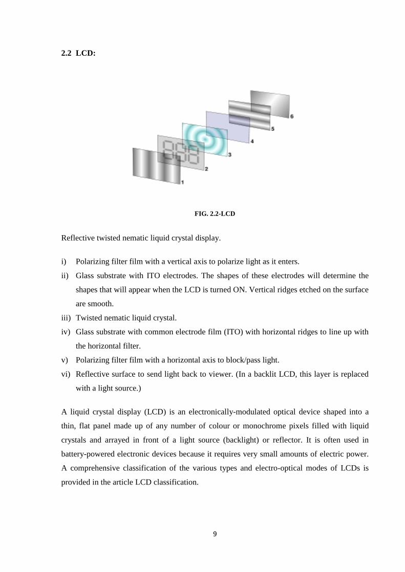
2.2 LCD:
FIG. 2.2-LCD
Reflective twisted nematic liquid crystal display.
i) Polarizing filter film with a vertical axis to polarize light as it enters.
ii) Glass substrate with ITO electrodes. The shapes of these electrodes will determine the
shapes that will appear when the LCD is turned ON. Vertical ridges etched on the surface
are smooth.
iii) Twisted nematic liquid crystal.
iv) Glass substrate with common electrode film (ITO) with horizontal ridges to line up with
the horizontal filter.
v) Polarizing filter film with a horizontal axis to block/pass light.
vi) Reflective surface to send light back to viewer. (In a backlit LCD, this layer is replaced
with a light source.)
A liquid crystal display (LCD) is an electronically-modulated optical device shaped into a
thin, flat panel made up of any number of colour or monochrome pixels filled with liquid
crystals and arrayed in front of a light source (backlight) or reflector. It is often used in
battery-powered electronic devices because it requires very small amounts of electric power.
A comprehensive classification of the various types and electro-optical modes of LCDs is
provided in the article LCD classification.

10
FIG2.3-LCD ALARM CLOCK
Each pixel of an LCD typically consists of a layer of molecules aligned between two
transparent electrodes, and two polarizing filters, the axes of transmission of which are (in
most of the cases) perpendicular to each other. With no actual liquid crystal between the
polarizing filters, light passing through the first filter would be blocked by the second
(crossed) polarizer. The surface of the electrodes that are in contact with the liquid crystal
material are treated so as to align the liquid crystal molecules in a particular direction. This
treatment typically consists of a thin polymer layer that is unidirectionally rubbed using, for
example, a cloth. The direction of the liquid crystal alignment is then defined by the direction
of rubbing. Electrodes are made of a transparent conductor called Indium Tin Oxide (ITO).
Before applying an electric field, the orientation of the liquid crystal molecules is determined
by the alignment at the surfaces. In a twisted nematic device (still the most common liquid
crystal device), the surface alignment directions at the two electrodes are perpendicular to
each other, and so the molecules arrange themselves in a helical structure, or twist. This
reduces the rotation of the polarization of the incident light, and the device appears grey. If
the applied voltage is large enough, the liquid crystal molecules in the centre of the layer are
almost completely untwisted and the polarization of the incident light is not rotated as it
passes through the liquid crystal layer. This light will then be mainly polarized perpendicular
to the second filter, and thus be blocked and the pixel will appear black. By controlling the
voltage applied across the liquid crystal layer in each pixel, light can be allowed to pass
through in varying amounts thus constituting different levels of gray. The optical effect of a
twisted nematic device in the voltage-on state is far less dependent on variations in the device

11
thickness than that in the voltage-off state. Because of this, these devices are usually operated
between crossed polarisers such that they appear bright with no voltage (the eye is much
more sensitive to variations in the dark state than the bright state). These devices can also be
operated between parallel polarisers, in which case the bright and dark states are reversed.
The voltage-off dark state in this configuration appears blotchy, however, because of small
variations of thickness across the device. Both the liquid crystal material and the alignment
layer material contain ionic compounds. If an electric field of one particular polarity is
applied for a long period of time, this ionic material is attracted to the surfaces and degrades
the device performance. This is avoided either by applying an alternating current or by
reversing the polarity of the electric field as the device is addressed (the response of the liquid
crystal layer is identical, regardless of the polarity of the applied field).
2.2.1 INTERFACING 16×2 LCD WITH 8051:
LCD display is an inevitable part in almost all embedded projects and this is about interfacing
16×2 LCD with 8051 microcontroller. Many guys find it hard to interface LCD module with
the 8051 but the fact is that if you learn it properly, it’s a very easy job and by knowing it you
can easily design embedded projects like digital voltmeter / ammeter, digital clock, home
automation displays, status indicator display, digital code locks, digital speedometer/
odometer, display for music players etc. Thoroughly going through this article will make you
able to display any text (including the extended characters) on any part of the 16×2 display
screen. In order to understand the interfacing first you have to know about the 16×2 LCD
module [1].
2.2.2 16×2 LCD MODULES:
16×2 LCD module is a very common type of LCD module that is used in 8051 based
embedded projects. It consists of 16 rows and 2 columns of 5×7 or 5×8 LCD dot matrices.
The module are talking about here is type number JHD162A which is a very popular one. It is
available in a 16 pin package with back light, contrast adjustment function and each dot
matrix has 5×8 dot resolution. The pin numbers, their name and corresponding functions are
shown in the table below.
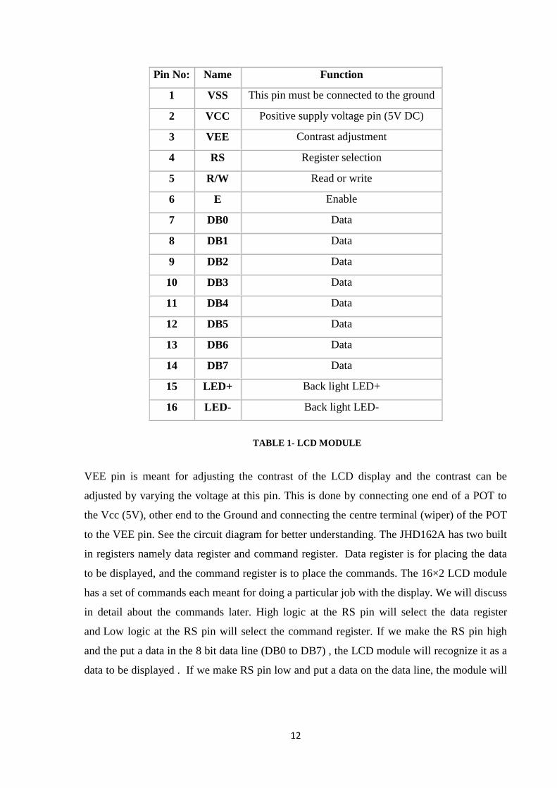
12
Pin No: Name Function
1 VSS This pin must be connected to the ground
2 VCC Positive supply voltage pin (5V DC)
3 VEE Contrast adjustment
4 RS Register selection
5 R/W Read or write
6 E Enable
7 DB0 Data
8 DB1 Data
9 DB2 Data
10 DB3 Data
11 DB4 Data
12 DB5 Data
13 DB6 Data
14 DB7 Data
15 LED+ Back light LED+
16 LED- Back light LED-
TABLE 1- LCD MODULE
VEE pin is meant for adjusting the contrast of the LCD display and the contrast can be
adjusted by varying the voltage at this pin. This is done by connecting one end of a POT to
the Vcc (5V), other end to the Ground and connecting the centre terminal (wiper) of the POT
to the VEE pin. See the circuit diagram for better understanding. The JHD162A has two built
in registers namely data register and command register. Data register is for placing the data
to be displayed, and the command register is to place the commands. The 16×2 LCD module
has a set of commands each meant for doing a particular job with the display. We will discuss
in detail about the commands later. High logic at the RS pin will select the data register
and Low logic at the RS pin will select the command register. If we make the RS pin high
and the put a data in the 8 bit data line (DB0 to DB7) , the LCD module will recognize it as a
data to be displayed . If we make RS pin low and put a data on the data line, the module will
13
recognize it as a command. R/W pin is meant for selecting between read and write modes.
High level at this pin enables read mode and low level at this pin enables write mode. E pin is
for enabling the module. A high to low transition at this pin will enable the module. DB0 to
DB7 are the data pins. The data to be displayed and the command instructions are placed on
these pins. LED+ is the anode of the back light LED and this pin must be connected to Vcc
through a suitable series current limiting resistor. LED- is the cathode of the back light LED
and this pin must be connected to ground.
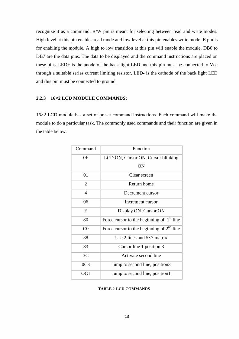
2.2.3 16×2 LCD MODULE COMMANDS:
16×2 LCD module has a set of preset command instructions. Each command will make the
module to do a particular task. The commonly used commands and their function are given in
the table below.
Command Function
0F LCD ON, Cursor ON, Cursor blinking
ON
01 Clear screen
2 Return home
4 Decrement cursor
06 Increment cursor
E Display ON ,Cursor ON
80 Force cursor to the beginning of 1st line
C0 Force cursor to the beginning of 2nd
line
38 Use 2 lines and 5×7 matrix
83 Cursor line 1 position 3
3C Activate second line
0C3 Jump to second line, position3
OC1 Jump to second line, position1
TABLE 2-LCD COMMANDS
14
2.2.4 LCD INITIALIZATION:
The steps that have to be done for initializing the LCD display is given below and these steps
are common for almost all applications.
i) Send 38H to the 8 bit data line for initialization
ii) Send 0FH for making LCD ON, cursor ON and cursor blinking ON.
iii) Send 06H for incrementing cursor position.
iv) Send 01H for clearing the display and return the cursor.
2.2.5 SENDING DATA TO THE LCD:
The steps for sending data to the LCD module are given below. It have been already
discussed that the LCD module has pins namely RS, R/W and E. It is the logic state of these
pins that make the module to determine whether a given data input is a command or data to
be displayed.
i) Make R/W low.
ii) Make RS=0 if data byte is a command and make RS=1 if the data byte is a data to be
displayed.
iii) Place data byte on the data register.
iv) Pulse E from high to low.
v) Repeat above steps for sending another data.
2.3 RFID:
Radio-frequency identification (RFID) is the use of an object (typically referred to as an
RFID tag) applied to or incorporated into a product, animal, or person for the purpose of
identification and tracking using radio waves. Some tags can be read from several meters
away and beyond the line of sight of the reader. Most RFID tags contain at least two parts.
One is an integrated circuit for storing and processing information, modulating and
demodulating a radio-frequency (RF) signal, and other specialized functions. The second is

15
an antenna for receiving and transmitting the signal. There are generally three types of RFID
tags: active RFID tags, which contain a battery and can transmit signals autonomously.
Passive RFID tags, which have no battery and require an external source to provoke signal
transmission. Battery assisted passive (BAP) which require an external source to wake up but
have significant higher forward link capability providing great read range. Today, RFID is
used in enterprise supply chain management to improve the efficiency of inventory tracking
and management.
2.3.1 HISTORY AND TECHNOLOGY BACKGROUND:
In 1946 Léon Theremin invented an espionage tool for the Soviet Union which retransmitted
incident radio waves with audio information. Sound waves vibrated a diaphragm which
slightly altered the shape of the resonator, which modulated the reflected radio frequency.
FIG 2.4-AN RFID TAG
Even though this device was a covert listening device, not an identification tag, it is
considered to be a predecessor of RFID technology, because it was likewise passive, being
energized and activated by electromagnetic waves from an outside source. Similar
technology, such as the IFF transponder invented in the United Kingdom in 1939, was
routinely used by the allies in World War II to identify aircraft as friend or foe. Transponders
are still used by most powered aircraft to this day. Another early work exploring RFID is the
landmark 1948 paper by Harry Stockman, titled "Communication by Means of Reflected
Power" (Proceedings of the IRE, pp 1196–1204, October 1948). Stockman predicted that "...
considerable research and development work has to be done before the remaining basic

16
problems in reflected-power communication are solved, and before the field of useful
applications is explored. "Mario Cardullo's U.S. Patent 3,713,148 in 1973 was the first true
ancestor of modern RFID; a passive radio transponder with memory. The initial device was
passive, powered by the interrogating signal, and was demonstrated in 1971 to the New York
Port Authority and other potential users and consisted of a transponder with 16 bit memory
for use as a toll device. The basic Cardullo patent covers the use of RF, sound and light as
transmission media. The original business plan presented to investors in 1969 showed uses in
transportation (automotive vehicle identification, automatic toll system, electronic license
plate, electronic manifest, vehicle routing, vehicle performance monitoring), banking
(electronic check book, electronic credit card), security (personnel identification, automatic
gates, surveillance) and medical (identification, patient history). A very early demonstration
of reflected power (modulated backscatter) RFID tags, both passive and semi-passive, was
performed by Steven Deep, Alfred Koelle, and Robert Freyman at the Los Alamos National
Laboratory in 1973. The portable system operated at 915 MHz and used 12-bit tags. This
technique is used by the majority of today's UHFID and microwave RFID tags. The first
patent to be associated with the abbreviation RFID was granted to Charles Walton in 1983
U.S. Patent 4,384,288. The largest deployment of active RFID is the US Department of
Defence use of Savi active tags on every one of its more than a million shipping containers
that travel outside of the continental United States (CONUS). The largest passive RFID
deployment is the Defence Logistics Agency (DLA) deployment across 72 facilities
implemented by ODIN who also performed the global roll-out for Airbus consisting of 13
projects across the globe.
2.3.2 MINIATURIZATION:
RFID is the technology which makes it easy to conceal or incorporate them in other items.
For example, in 2009 researchers at Bristol University successfully glued RFID micro
transponders to live ants in order to study their behaviour. This trend towards increasingly
miniaturized RFID is likely to continue as technology advances. However, the ability to read
at distance is limited by the inverse-square law. Hitachi holds the record for the smallest
RFID chip, at 0.05mm x 0.05mm. The Mu chip tags are 64 times smaller than the new RFID
tags. Manufacture is enabled by using the Silicon-on-Insulator (SOI) process. These "dust"
17
sized chips can store 38-digit numbers using 128-bit Read Only Memory (ROM). A major
challenge is the attachment of the antennas, thus limiting read range to only millimetres.
Potential alternatives to the radio frequencies (0.125–0.1342, 0.140–0.1485, 13.56, and 840–
960 MHz) used are seen in optical RFID (or OPID) at 333 THz (900 nm), 380 THz (788 nm),
750 THz (400 nm). The awkward antennas of RFID can be replaced with photovoltaic
components and IR-LEDs on the ICs [4].
2.4 GSM:
GSM/GPRS module is used to establish communication between a computer and a GSM-
GPRS system. Global System for Mobile communication (GSM) is an architecture used for
mobile communication in most of the countries. Global Packet Radio Service (GPRS) is an
extension of GSM that enables higher data transmission rate. GSM/GPRS module consists of
a GSM/GPRS modem assembled together with power supply circuit and communication
interfaces (like RS-232, USB, etc) for computer. The MODEM is the soul of such modules.
Wireless MODEMs are the MODEM devices that generate, transmit or decode data from a
cellular network, for establishing communication between the cellular network and the
computer. These are manufactured for specific cellular network (GSM/UMTS/CDMA) or
specific cellular data standard (GSM/UMTS/GPRS/EDGE/HSDPA) or technology
(GPS/SIM). Wireless MODEMs like other MODEM devices use serial communication to
interface with and need Hayes compatible AT commands for communication with the
computer (any microprocessor or microcontroller system). GSM/GPRS MODEM is a class of
wireless MODEM devices that are designed for communication of a computer with the GSM
and GPRS network. It requires a SIM (Subscriber Identity Module) card just like mobile
phones to activate communication with the network. Also they have IMEI (International
Mobile Equipment Identity) number similar to mobile phones for their identification. A
GSM/GPRS MODEM can perform the following operations:
i) Receive, send or delete SMS messages in a SIM.
ii) Read, add, search phonebook entries of the SIM.
iii) Make, Receive, or reject a voice call.
18
The MODEM needs AT commands, for interacting with processor or controller, which are
communicated through serial communication. These commands are sent by the
controller/processor. The MODEM sends back a result after it receives a command. Different
AT commands supported by the MODEM can be sent by the processor/controller/computer
to interact with the GSM and GPRS cellular network. A GSM/GPRS module assembles a
GSM/GPRS modem with standard communication interfaces like RS-232 (Serial Port), USB
etc., so that it can be easily interfaced with a computer or a microprocessor / microcontroller
based system. The power supply circuit is also built in the module that can be activated by
using a suitable adaptor. Throughout the evolution of cellular telecommunications, various
systems have been developed without the benefit of standardized specifications. This
presented many problems directly related to compatibility, especially with the development
of digital radio technology. The GSM standard is intended to address these problems. From
1982 to 1985 discussions were held to decide between building an analog or digital system.
After multiple field tests, a digital system was adopted for GSM. The next task was to decide
between a narrow or broadband solution. In May 1987, the narrowband time division multiple
access (TDMA) solution was chosen.
2.4.1 THE GSM NETWORK:
GSM provides recommendations, not requirements. The GSM specifications define the
functions and interface requirements in detail but do not address the hardware. The reason for
this is to limit the designers as little as possible but still to make it possible for the operators
to buy equipment from different suppliers. The GSM network is divided into three major
systems: the switching system (SS), the base station system (BSS), and the operation and
support system (OSS). The basic GSM network elements are shown in Figure.
2.4.1.1 THE SWITCHING SYSTEM
The switching system (SS) is responsible for performing call processing and subscriber-
related functions. The switching system includes the following functional units:
19
i) HOME LOCATION REGISTERS (HLR)—The HLR is a database used for storage
and management of subscriptions. The HLR is considered the most important database,
as it stores permanent data about subscribers, including a subscriber's service profile,
location information, and activity status. When an individual buys a subscription from
one of the PCS operators, he or she is registered in the HLR of that operator.
ii) MOBILE SERVICES SWITCHING CENTRE (MSC)—The MSC performs the
telephony switching functions of the system. It controls calls to and from other telephone
and data systems. It also performs such functions as toll ticketing, network interfacing,
common channel signalling, and others.
iii) VISITOR LOCATION REGISTERS (VLR)—The VLR is a database that contains
temporary information about subscribers that is needed by the MSC in order to service
visiting subscribers. The VLR is always integrated with the MSC. When a mobile station
roams into a new MSC area, the VLR connected to that MSC will request data about the
mobile station from the HLR. Later, if the mobile station makes a call, the VLR will have
the information needed for call setup without having to interrogate the HLR each time.
iv) AUTHENTICATION CENTRE (AUC)—A unit called the AUC provides
authentication and encryption parameters that verify the user's identity and ensure the
confidentiality of each call. The AUC protects network operators from different types of
fraud found in today's cellular world.
v) EQUIPMENT IDENTITY REGISTER (EIR)—The EIR is a database that contains
information about the identity of mobile equipment that prevents calls from stolen,
unauthorized, or defective mobile stations. The AUC and EIR are implemented as stand-
alone nodes or as a combined AUC/EIR node.
2.4.1.2 THE BASE STATION SYSTEM (BSS):
All radio-related functions are performed in the BSS, which consists of base station
controllers (BSCs) and the base transceiver stations (BTSs).

20
i) BSC- The BSC provides all the control functions and physical links between the MSC
and BTS. It is a high-capacity switch that provides functions such as handover, cell
configuration data, and control of radio frequency (RF) power levels in base transceiver
stations. A number of BSCs are served by an MSC.
ii) BTS- The BTS handles the radio interface to the mobile station. The BTS is the radio
equipment (transceivers and antennas) needed to service each cell in the network. A
group of BTSs are controlled by a BSC [5].
FIG. 2.5-GSM

21
2.5 REGULATOR 7805:
The series of fixed-voltage integrated-circuit voltage regulators is designed for a wide range
of applications. These applications include on-card regulation for elimination of noise and
distribution problems associated with single-point regulation. Each of these regulators can
deliver up to 1.5 A of output current. The internal current-limiting and thermal-shutdown
features of these regulators essentially make them immune to overload. In addition to use as
fixed-voltage regulators, these devices can be used with external components to obtain
adjustable output voltages and currents, and also can be used as the power-pass element in
precision regulators. 7805 is a voltage regulator integrated circuit. It is a member of 78xx
series of fixed linear voltage regulator ICs. The voltage source in a circuit may have
fluctuations and would not give the fixed voltage output. The voltage regulator IC maintains
the output voltage at a constant value. The xx in 78xx indicates the fixed output voltage it is
designed to provide. 7805 provides +5V regulated power supply. Capacitors of suitable
values can be connected at input and output pins depending upon the respective voltage
levels.
FIG. 2.6-PIN DIAGRAM
2.5.1 PIN DESCRIPTION:
Pin No Function Name
1 Input voltage (5V-18V) Input
2 Ground (0V) Ground
3 Regulated output; 5V (4.8V-5.2V) Output
22
2.6 CRYSTAL OSCILLATOR:
A crystal oscillator is an electronic oscillator circuit that uses the mechanical resonance of a
vibrating crystal of piezoelectric material to create an electrical signal with a very precise
frequency. This frequency is commonly used to keep track of time, to provide a stable clock
signal for digital integrated circuit and to stabilize frequencies for radio transmitter and
receivers. The most common type of piezoelectric resonator used in the quartz crystal, so
oscillator circuit incorporating them became known as crystal oscillator, but other
piezoelectric material including polycrystalline ceramic is used in similar circuit.
FIG. 2.7-CRYSTAL OSCILLATOR
23
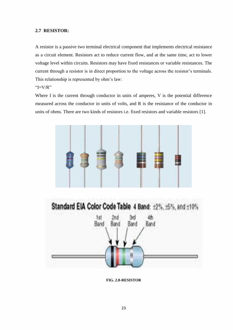
2.7 RESISTOR:
A resistor is a passive two terminal electrical component that implements electrical resistance
as a circuit element. Resistors act to reduce current flow, and at the same time, act to lower
voltage level within circuits. Resistors may have fixed resistances or variable resistances. The
current through a resistor is in direct proportion to the voltage across the resistor’s terminals.
This relationship is represented by ohm’s law:
“I=V/R”
Where I is the current through conductor in units of amperes, V is the potential difference
measured across the conductor in units of volts, and R is the resistance of the conductor in
units of ohms. There are two kinds of resistors i.e. fixed resistors and variable resistors [1].
FIG. 2.8-RESISTOR

24
COLOR
1ST
BAND
2ND
BAND
3RD
BAND
4TH
BAND
Black 0 0 100
Brown 1 1 101
Red 2 2 102
2%
Orange 3 3 103
Yellow 4 4 104
Green 5 5 105
Blue 6 6 106
Violet 7 7 107
Gray 8 8 108
White 9 9 109
Gold 10-1
5%
Silver 10-2
10%
TABLE 3-COLOUR CODE
2.8 CAPACITOR:
A capacitor consists of two conductors separated by a non-conductive region. The non-
conductive region is called the dielectric. In simpler terms, the dielectric is just an electrical
insulator. Examples of dielectric media are glass, air, paper, vacuum, and even
a semiconductor depletion region chemically identical to the conductors. A capacitor is
assumed to be self-contained and isolated, with no net electric charge and no influence from
any external electric field. The conductors thus hold equal and opposite charges on their
facing surfaces, and the dielectric develops an electric field. In SI units, a capacitance of
one farad means that one coulomb of charge on each conductor causes a voltage of
one volt across the device. An ideal capacitor is wholly characterized by a
constant capacitance C, defined as the ratio of charge ±Q on each conductor to the
voltage V between them:
Because the conductors (or plates) are close together, the opposite charges on the conductors
attract one another due to their electric fields, allowing the capacitor to store more charge for
a given voltage than if the conductors were separated, giving the capacitor a large
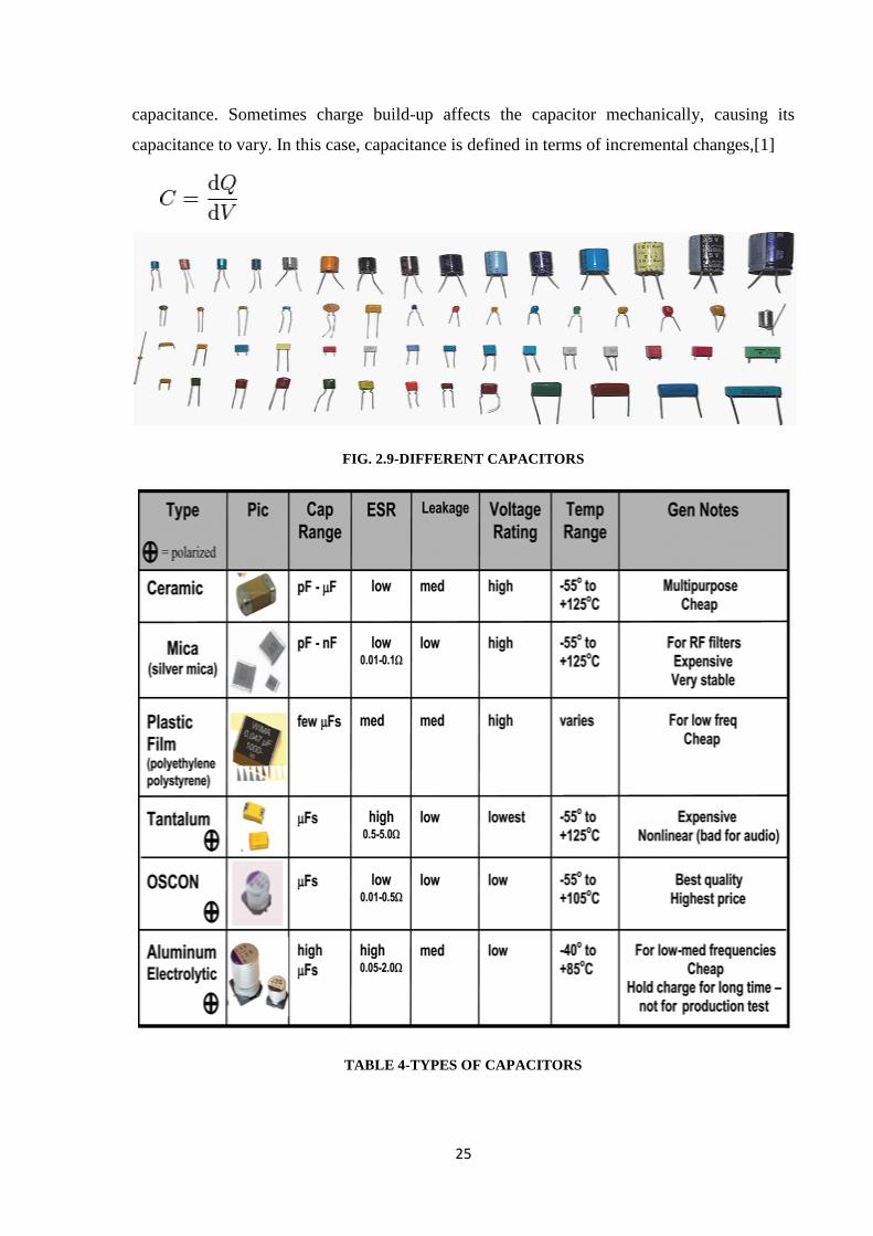
25
capacitance. Sometimes charge build-up affects the capacitor mechanically, causing its
capacitance to vary. In this case, capacitance is defined in terms of incremental changes,[1]
FIG. 2.9-DIFFERENT CAPACITORS
TABLE 4-TYPES OF CAPACITORS

26
2.9 LEDs:
FIG. 2.10-LED SYMBOL
2.9.1 THEORY:
A Light emitting diode (LED) is essentially a pn junction diode. When carriers are injected
across a forward-biased junction, it emits incoherent light. Most of the commercial LEDs are
realized using a highly doped n and a p Junction.
FIG.2.11-P-N+ JUNCTION UNDER UNBIASED AND BIASED CONDITIONS. (PN JUNCTION
DEVICES AND LIGHT EMITTING DIODES BY SAFA KASAP).
To understand the principle, let’s consider an unbiased pn+ junction (Figure1 shows the pn+
energy band diagram). The depletion region extends mainly into the p-side. There is a
potential barrier from Ec on the n-side to the Ec on the p-side, called the built-in voltage, V0.

27
This potential barrier prevents the excess free electrons on the n+ side from diffusing into the
p side. When a Voltage V is applied across the junction, the built-in potential is reduced from
V0 to V0 – V. This allows the electrons from the n+ side to get injected into the p-side. Since
Electrons are the minority carriers in the p-side, this process is called minority carrier
injection. But the hole injection from the p side to n+ side is very less and so the current is
primarily due to the flow of electrons into the p-side. These electrons injected into the p-side
recombine with the holes. This recombination results in spontaneous emission of photons
(light). This effect is called injection Electro luminescence. These photons should be allowed
to escape from the device without being reabsorbed. The recombination can be classified into
the following two kinds:
i) Direct recombination
ii) Indirect recombination
i) DIRECT RECOMBINATION:
In direct band gap materials, the minimum energy of the conduction band lies directly above
the maximum energy of the valence band in momentum space energy (Figure 2 shows the E-
k plot (see Appendix 2) of a direct band gap material). In this material, free electrons at the
bottom of the conduction band can recombine directly with free holes at the top of the
valence band, as the momentum of the two particles is the same. This transition from
conduction band to valence band involves photon emission (takes care of the principle of
energy conservation). This is known as direct recombination. Direct recombination occurs
spontaneously. GaAs is an example of a direct band-gap material.
FIG.2.12-DIRECT BANDGAP AND DIRECT RECOMBINATION

28
ii) INDIRECT RECOMBINATION:
In the indirect band gap materials, the minimum energy in the conduction band is shifted by a
k-vector relative to the valence band. The k-vector difference represents a difference in
momentum. Due to this difference in momentum, the probability of direct electronhole
recombination is less. In these materials, additional dopants(impurities) are added which form
very shallow donor states. These donor states capture the free electrons locally; provides the
necessary momentum shift for recombination. These donor states serve as the recombination
centers. This is called Indirect (non-radiative) Recombination. Figure3 shows the E-k plot of
an indirect band gap material and an example of how Nitrogen serves as a recombination
center in GaAsP. In this case it creates a donor state, when SiC is doped with Al, it
recombination takes place through an acceptor level. The indirect recombination should
satisfy both conservation energy, and momentum. Thus besides a photon emission, phonon
emission or absorption has to take place. GaP is an example of an indirect band-gap material.
FIG.2.13-INDIRECT BANDGAP AND NONRADIATIVE RECOMBINATION
The wavelength of the light emitted, and hence the color, depends on the band gap energy
of the materials forming the p-n junction. The emitted photon energy is approximately equal
to the band gap energy of the semiconductor. The following equation relates the wavelength
and the energy band gap.
29
hν = Eg
hc/λ = Eg
λ = hc/ Eg
Where h is Plank’s constant, c is the speed of the light and Eg is the energy band gap Thus, a
semiconductor with a 2 eV band-gap emits light at about 620 nm, in the red. A 3 eV band-gap
material would emit at 414 nm, in the violet. Appendix 4 shows a list of semiconductor
materials and the corresponding colors.
2.9.2 LED MATERIALS:
An important class of commercial LEDs that cover the visible spectrum are the III-V. ternary
alloys based on alloying GaAs and GaP which are denoted by GaAs1-yPy. In GaAlP is an
example of a quarternary (four element) III-V alloy with a direct bandgap. The LEDs realized
using two differently doped semiconductors that are the same material is called a
homojunction. When they are realized using different bandgap materials they are called a
heterostructure device. A heterostructure LED is brighter than a Homo Junction LED.
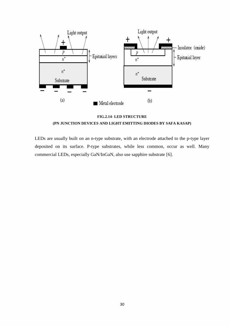
2.9.3 LED STRUCTURE:
The LED structure plays a crucial role in emitting light from the LED surface. The LEDs are
structured to ensure most of the recombination takes place on the surface by the following
two ways.
i) By increasing the doping concentration of the substrate, so that additional free minority
charge carriers electrons move to the top, recombine and emit light at the surface.
ii) By increasing the diffusion length L = √ Dτ, where D is the diffusion coefficient and τ is
the carrier life time. But when increased beyond a critical length there is a chance of re-
absorption of the photons into the device.
The LED has to be structured so that the photons generated from the device are emitted
without being reabsorbed. One solution is to make the p layer on the top thin, enough to
create a depletion layer. Following picture shows the layered structure. There are different
ways to structure the dome for efficient emitting.
30
FIG.2.14- LED STRUCTURE
(PN JUNCTION DEVICES AND LIGHT EMITTING DIODES BY SAFA KASAP)
LEDs are usually built on an n-type substrate, with an electrode attached to the p-type layer
deposited on its surface. P-type substrates, while less common, occur as well. Many
commercial LEDs, especially GaN/InGaN, also use sapphire substrate [6].

31
Chapter 3
HARDWARE DESCRIPTION
3.1 CIRCUIT DIAGRAM:
FIG. 3.1-CIRCUIT DIAGRAM OF FTC
In this circuit diagram, we have a Microcontroller AT89S52. It is interfaced with the RFID
reader, RFID tag, LEDs, LCD, Power Supply and GSM Module. The AT89S52 is a 40 pin
microcontroller it has P0, P1, P2 and P3 ports. The LCD is connected at the P2 port of the
microcontroller. Reset, receiver and transmitter are at pin no. 9, 10 and 11 of the
microcontroller respectively. LEDs are connected at the pin no. 1, 2 and 3. The power supply
is given through RFID reader module, the transmitter of RFID reader module is connected to
the receiver of the microcontroller. The GSM is further connected with the microcontroller;
the transmitter of microcontroller is connected with the receiver of the GSM module. And by
all this connection system works.
32
3.2 WORKING:
In this project, there is depiction of Traffic Signal Lights. Here in this, a RFID reader is
placed over the traffic light stamp, and this the reader is deactivated in the green and yellow
signal and when the signal is red i.e. the prohibition of vehicles to move forward. If vehicle
crosses the red signal, means he breaks the rules then RFID reader reads the high security
number plate of the vehicle there is encrypted unique id in that number plate. Now, that
unique id is transmitted to the microcontroller and its received by the receiver of
microcontroller and then transmitted to GSM module and from there, using SIM card the
unique id is sent to the control room where the database of unique id is saved. From there the
further enquiry takes place according to the norms and rules.

33
Chapter 4
SOFTWARE DESCRIPTION
4.1 INTRODUCTION TO MICRO VISION KEIL:
It is possible to create the source files in a text editor such as Notepad, run the Compiler on
each C source file, specifying a list of controls, run the Assembler on each Assembler source
file, specifying another list of controls, run either the Library Manager or Linker (again
specifying a list of controls) and finally running the Object-HEX Converter to convert the
Linker output file to an Intel Hex File. Once that has been completed the Hex File can be
downloaded to the target hardware and debugged. Alternatively KEIL can be used to create
source files; automatically compile, link and covert using options set with an easy to use user
interface and finally simulate or perform debugging on the hardware with access to C
variables and memory. Unless you have to use the tolls on the command line, the choice is
clear. KEIL Greatly simplifies the process of creating and testing an embedded application.
4.1.1 PROJECTS:
The user of KEIL centres on “projects”. A project is a list of all the source files required to
build a single application, all the tool options which specify exactly how to build the
application, and – if required – how the application should be simulated. A project contains
enough information to take a set of source files and generate exactly the binary code required
for the application. Because of the high degree of flexibility required from the tools, there are
many options that can be set to configure the tools to operate in a specific manner. It would
be tedious to have to set these options up every time the application is being built; therefore
they are stored in a project file. Loading the project file into KEIL informs KEIL which
source files are required, where they are, and how to configure the tools in the correct way.
KEIL can then execute each tool with the correct options. It is also possible to create new
projects in KEIL. Source files are added to the project and the tool options are set as required.
The project can then be saved to preserve the settings.
34
The project also stores such things as which windows were left open in the
simulator/debugger, so when a project is reloaded and the simulator or debugger started, all
the desired windows are opened. KEIL project files have the extension.
4.1.2 SIMULATOR/DEBUGGER :
The simulator/ debugger in KEIL can perform a very detailed simulation of a micro controller
along with external signals. It is possible to view the precise execution time of a single
assembly instruction, or a single line of C code, all the way up to the entire application,
simply by entering the crystal frequency. A window can be opened for each peripheral on the
device, showing the state of the peripheral. This enables quick trouble shooting of mis-
configured peripherals. Breakpoints may be set on either assembly instructions or lines of C
code, and execution may be stepped through one instruction or C line at a time. The contents
of all the memory areas may be viewed along with ability to find specific variables. In
addition the registers may be viewed allowing a detailed view of what the microcontroller is
doing at any point in time.
The Keil Software 8051 development tools listed below are the programs you use to compile
your C code, assemble your assembler source files, link your program together, create HEX
files, and debug your target program. µVision2 for Windows™ Integrated Development
Environment: combines Project Management, Source Code Editing, and Program Debugging
in one powerful environment.
i) C51 ANSI Optimizing C Cross Compiler: creates relocatable object modules from your
C source code,
ii) A51 Macro Assembler: creates relocatable object modules from your 8051
assembler source code,
iii) BL51 Linker/Locator: combines relocatable object modules created by the compiler and
assembler into the final absolute object module,
iv) LIB51 Library Manager: combines object modules into a library, which may be used by
the linker,
v) OH51 Object-HEX Converter: creates Intel HEX files from absolute object modules.
35
4.1.3 CONCEPT OF COMPILER:
Compilers are programs used to convert a High Level Language to object code. Desktop
compilers produce an output object code for the underlying microprocessor, but not for other
microprocessors. I.E the programs written in one of the HLL like ‘C’ will compile the code to
run on the system for a particular processor like x86 (underlying microprocessor in the
computer). For example compilers for Dos platform is different from the Compilers for Unix
platform. So if one wants to define a compiler then compiler is a program that
translates source code into object code. The compiler derives its name from the way it works,
looking at the entire piece of source code and collecting and reorganizing the instruction. See
there is a bit little difference between compiler and an interpreter. Interpreter just interprets
whole program at a time while compiler analyzes and execute each line of source code in
succession, without looking at the entire program. The advantage of interpreters is that they
can execute a program immediately. Secondly programs produced by compilers run much
faster than the same programs executed by an interpreter. However compilers require some
time before an executable program emerges. Now as compilers translate source code into
object code, which is unique for each type of computer, many compilers are available for the
same language.
4.1.4 CONCEPT OF CROSS COMPILER:
A cross compiler is similar to the compilers but we write a program for the target processor
(like 8051 and its derivatives) on the host processors (like computer of x86). It means being
in one environment you are writing a code for another environment is called cross
development. And the compiler used for cross development is called cross compiler. So the
definition of cross compiler is a compiler that runs on one computer but produces object
code for a different type of computer. Cross compilers are used to generate software that can
run on computers with a new architecture or on special-purpose devices that cannot host their
own compilers. Cross compilers are very popular for embedded development, where the
target probably couldn't run a compiler. Typically an embedded platform has restricted RAM,
no hard disk, and limited I/O capability. Code can be edited and compiled on a fast host
machine (such as a PC or Unix workstation) and the resulting executable code can then be
36
downloaded to the target to be tested. Cross compilers are beneficial whenever the host
machine has more resources (memory, disk, I/O etc) than the target. Keil C Compiler is one
such compiler that supports a huge number of host and target combinations. It supports as a
target to 8 bit microcontrollers like Atmel and Motorola etc.
4.1.4.1 ADVANTAGES OF CROSS COMPILER:
There are several advantages of using cross compiler. Some of them are described as follows
i) By using this compilers not only can development of complex embedded systems be
completed in a fraction of the time, but reliability is improved, and maintenance is easy.
ii) Knowledge of the processor instruction set is not required.
iii) A rudimentary knowledge of the 8051’s memory architecture is desirable but not
necessary.
iv) Register allocation and addressing mode details are managed by the compiler.
v) The ability to combine variable selection with specific operations improves program
readability.
vi) Keywords and operational functions that more nearly resemble the human thought
process can be used.
vii) Program development and debugging times are dramatically reduced when compared to
assembly language programming.
viii) The library files that are supplied provide many standard routines (such as formatted
output, data conversions, and floating-point arithmetic) that may be incorporated into
your application.
ix) Existing routine can be reused in new programs by utilizing the modular programming
techniques available with C.
x) The C language is very portable and very popular. C compilers are available for almost
all target systems. Existing software investments can be quickly and easily converted
from or adapted to other processors or environments.
Now after going through the concept of compiler and cross compilers lets we start with Keil
C cross compiler.

37
4.1.5 KEIL C CROSS COMPILER:
Keil is a German based Software development company. It provides several development
tools like
i) IDE (Integrated Development environment)
ii) Project Manager
iii) Simulator
iv) Debugger
v) C Cross Compiler , Cross Assembler, Locator/Linker
Keil Software provides you with software development tools for the 8051 family of
microcontrollers. With these tools, you can generate embedded applications for the multitude
of 8051 derivatives. Keil provides following tools for 8051 development.
i) C51 Optimizing C Cross Compiler,
ii) A51 Macro Assembler,
iii) 8051 Utilities (linker, object file converter, library manager),
iv) Source-Level Debugger/Simulator,
v) µVision for Windows Integrated Development Environment.
The keil 8051 tool kit includes three main tools, assembler, compiler and linker. An
assembler is used to assemble your 8051 assembly program. A compiler is used to compile
your C source code into an object file. A linker is used to create an absolute object module
suitable for your in-circuit emulator.
8052 project development cycle; these are the steps to develop 8051 project using keil
i) Create source files in C or assembly.
ii) Compile or assemble source files.
iii) Correct errors in source files.
iv) Link object files from compiler and assembler.
v) Test linked application.
38
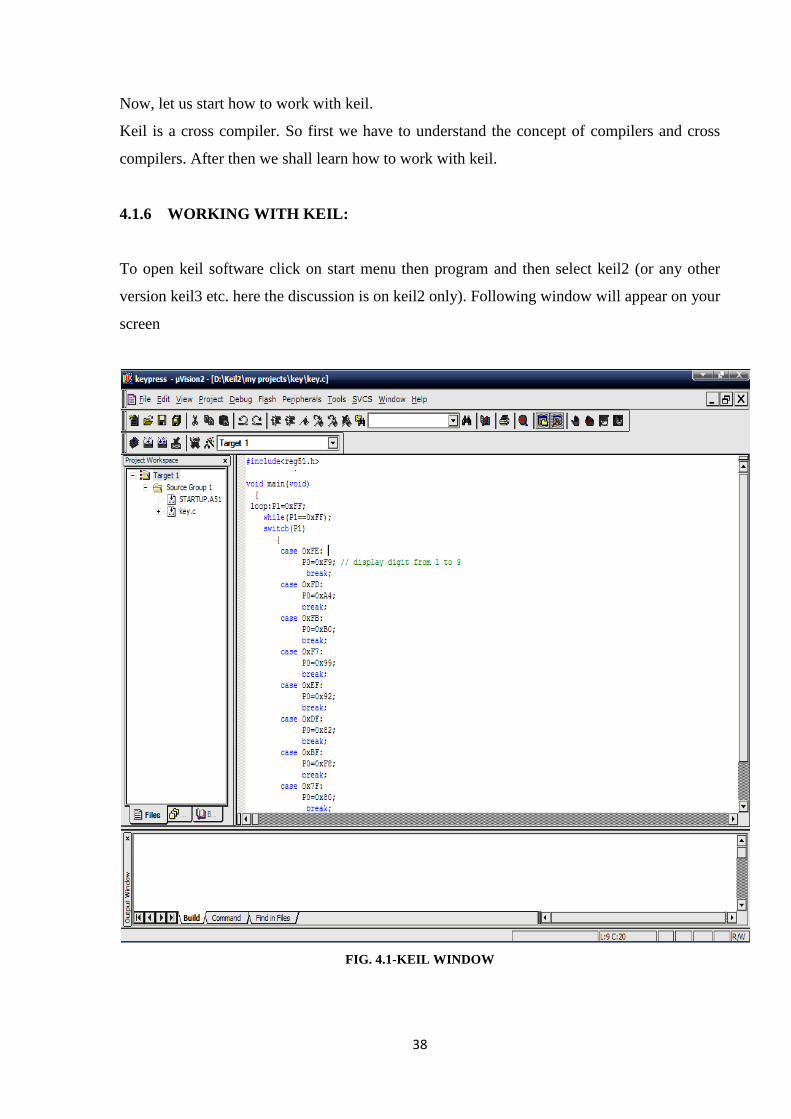
Now, let us start how to work with keil.
Keil is a cross compiler. So first we have to understand the concept of compilers and cross
compilers. After then we shall learn how to work with keil.
4.1.6 WORKING WITH KEIL:
To open keil software click on start menu then program and then select keil2 (or any other
version keil3 etc. here the discussion is on keil2 only). Following window will appear on your
screen
FIG. 4.1-KEIL WINDOW

39
You can see three different windows in this screen.
i) Project work space window, It is for showing all the related files connected with your
project.
ii) Editing window, It is the place where you will edit the code.
iii) Output window, It will show the output when you compile or build or run your project.
Now to start with new project follow the steps:
1) Click on project menu and select new project
2) You will be asked to create new project in specific directory
3) Just move to your desired directory and there create a new folder for your project named
"first". Here I am creating new project in d:\keil2\myprojects\first as shown in figure
FIG. 4.2-PROJECT MENU
4) Give the name of project as "test". By default it will be saved as *.v2 extension.

40
5) Now you will be asked to chose your target device for which you want to write the
program.
6) Scroll down the cursor and select generic from list. expand the list and select 8051 (all
variants)
FIG. 4.3-TARGET WINDOW
when you click OK, you will be asked to add startup code and file to your project folder.
click yes. Now on your screen expand target1 list fully. You will see following window

41
FIG. 4.4-TARGET LIST
7) Now click on file menu and select new file. editor window will open. Now you can start
writing your code.
8) As you start writing program in C, same way here also you have to first include the
header file. Because our target is 8051 our header file will be "reg51.h"
42
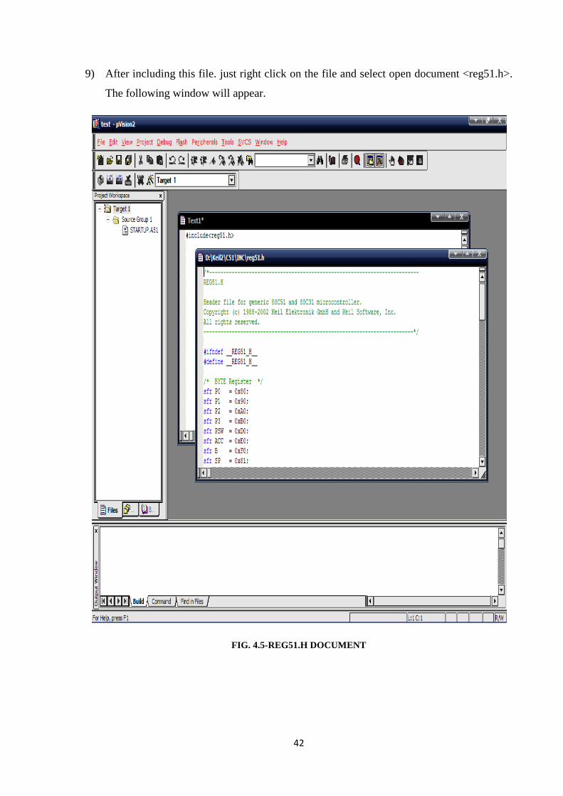
9) After including this file. just right click on the file and select open document <reg51.h>.
The following window will appear.
FIG. 4.5-REG51.H DOCUMENT
43
10) If you scroll down cursor you will see that all the SFRs like P0-P3, TCON, TMOD,
ACC, bit registers and byte registers are already defined in this header file. so one can
directly use these register names in coding
11) Now you can write your program same as c language starting with void main()
12) After completing the code save the file in project folder with ".c" extension.
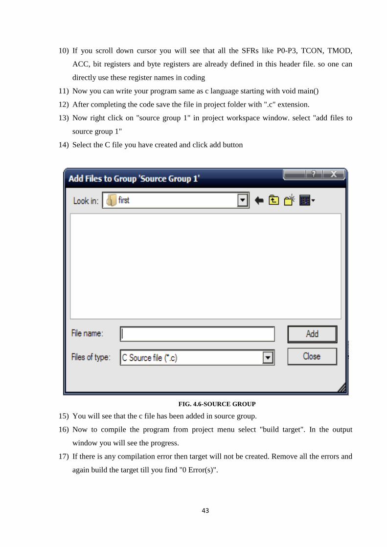
13) Now right click on "source group 1" in project workspace window. select "add files to
source group 1"
14) Select the C file you have created and click add button
FIG. 4.6-SOURCE GROUP
15) You will see that the c file has been added in source group.
16) Now to compile the program from project menu select "build target". In the output
window you will see the progress.
17) If there is any compilation error then target will not be created. Remove all the errors and
again build the target till you find "0 Error(s)".
44
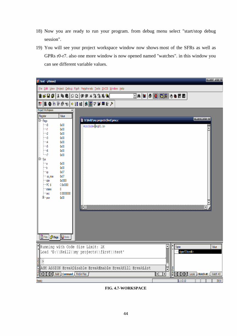
18) Now you are ready to run your program. from debug menu select "start/stop debug
session".
19) You will see your project workspace window now shows most of the SFRs as well as
GPRs r0-r7. also one more window is now opened named "watches". in this window you
can see different variable values.
FIG. 4.7-WORKSPACE
45
20) To add variable in watch window goto "watch#1" tab. then type F2 to edit and type the
name of your variable.
21) If you want to see the output on ports go to peripheral menu and select I/O ports. select
the desire port. you can give input to port pins by checking or unchecking any check box.
here the check mark means digit 1 and no check mark means 0. the output on the pin will
be shown in same manner.
22) To run the program you can use any of the option provided "go", "step by step", "step
forward", "step ove" etc.
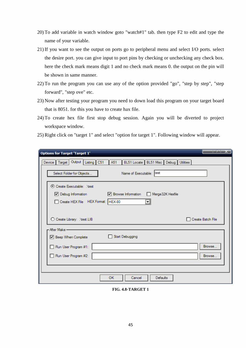
23) Now after testing your program you need to down load this program on your target board
that is 8051. for this you have to create hax file.
24) To create hex file first stop debug session. Again you will be diverted to project
workspace window.
25) Right click on "target 1" and select "option for target 1". Following window will appear.
FIG. 4.8-TARGET 1
46
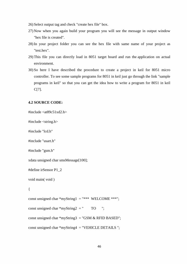
26) Select output tag and check "create hex file" box.
27) Now when you again build your program you will see the message in output window
"hex file is created".
28) In your project folder you can see the hex file with same name of your project as
"test.hex".
29) This file you can directly load in 8051 target board and run the application on actual
environment.
30) So here I have described the procedure to create a project in keil for 8051 micro
controller. To see some sample programs for 8051 in keil just go through the link "sample
programs in keil" so that you can get the idea how to write a program for 8051 in keil
C[7].
4.2 SOURCE CODE:
#include <at89c51xd2.h>
#include <string.h>
#include "lcd.h"
#include "usart.h"
#include "gsm.h"
xdata unsigned char smsMessage[100];
#define irSensor P1_2
void main( void )
const unsigned char *myString1 = "*** WELCOME ***";
const unsigned char *myString2 = " TO ";
const unsigned char *myString3 = "GSM & RFID BASED";
const unsigned char *myString4 = "VEHICLE DETAILS ";
47
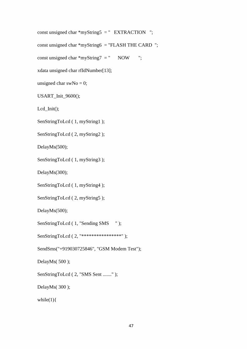
const unsigned char *myString5 = " EXTRACTION ";
const unsigned char *myString6 = "FLASH THE CARD ";
const unsigned char *myString7 = " NOW ";
xdata unsigned char rfIdNumber[13];
unsigned char swNo = 0;
USART_Init_9600();
Lcd_Init();
SenStringToLcd ( 1, myString1 );
SenStringToLcd ( 2, myString2 );
DelayMs(500);
SenStringToLcd ( 1, myString3 );
DelayMs(300);
SenStringToLcd ( 1, myString4 );
SenStringToLcd ( 2, myString5 );
DelayMs(500);
SenStringToLcd ( 1, "Sending SMS " );
SenStringToLcd ( 2, "****************" );
SendSms("+919030725846", "GSM Modem Test");
DelayMs( 500 );
SenStringToLcd ( 2, "SMS Sent ......." );
DelayMs( 300 );
while(1)
48
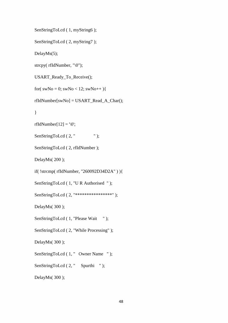
SenStringToLcd ( 1, myString6 );
SenStringToLcd ( 2, myString7 );
DelayMs(5);
strcpy( rfIdNumber, "\0");
USART_Ready_To_Receive();
for( swNo = 0; swNo < 12; swNo++ )
rfIdNumber[swNo] = USART_Read_A_Char();
rfIdNumber[12] = '\0';
SenStringToLcd ( 2, " " );
SenStringToLcd ( 2, rfIdNumber );
DelayMs( 200 );
if( !strcmp( rfIdNumber, "260092D34D2A" ) )
SenStringToLcd ( 1, "U R Authorised " );
SenStringToLcd ( 2, "****************" );
DelayMs( 300 );
SenStringToLcd ( 1, "Please Wait " );
SenStringToLcd ( 2, "While Processing" );
DelayMs( 300 );
SenStringToLcd ( 1, " Owner Name " );
SenStringToLcd ( 2, " Spurthi " );
DelayMs( 300 );

49
SenStringToLcd ( 1, " Vehicle No " );
SenStringToLcd ( 2, " AP 29 AD 9623 " );
DelayMs( 300 );
SenStringToLcd ( 1, "Colour: Black " );
SenStringToLcd ( 2, "Model : Pleasure" );
DelayMs( 300 );
while( irSensor == 0 );
SenStringToLcd ( 1, "Detected Signal " );
SenStringToLcd ( 2, "Breaking..... " );
DelayMs( 300 );
SenStringToLcd ( 1, "Sending SMS " );
SenStringToLcd ( 2, "****************" );
strcpy( smsMessage, "Name: Spurthi, Reg No: AP29 AD 9623, Colour: Black, Model:
Pleasure" );
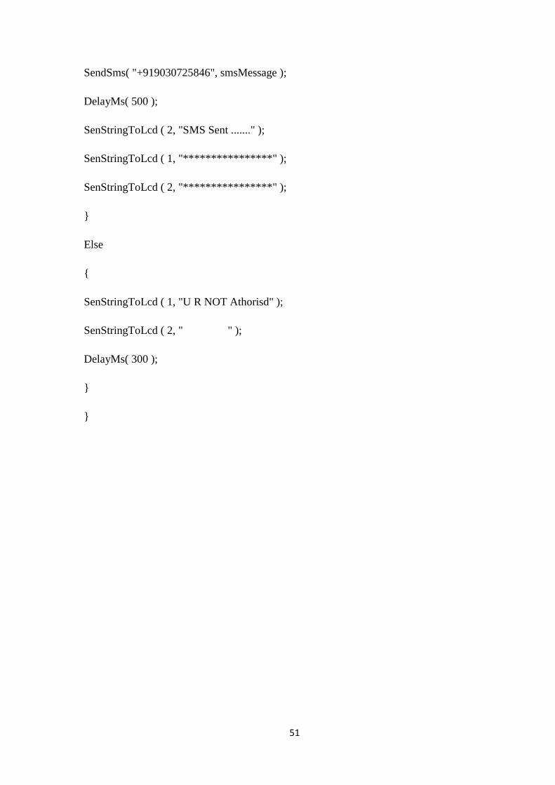
SendSms( "+919030725846", smsMessage );
DelayMs( 500 );
SenStringToLcd ( 2, "SMS Sent ......." );
SenStringToLcd ( 1, "****************”);
SenStringToLcd ( 2, "****************" );
else if( !strcmp( rfIdNumber, "26009354C524" ) )
SenStringToLcd ( 1, "U R Authorised " );
50
SenStringToLcd ( 2, "****************" );
DelayMs( 300 );
SenStringToLcd ( 1, "Please Wait " );
SenStringToLcd ( 2, "While Processing" );
DelayMs( 300 );
SenStringToLcd ( 1, " Owner Name " );
SenStringToLcd ( 2, " Bhavani " );
DelayMs( 300 );
SenStringToLcd ( 1, " Vehicle No " );
SenStringToLcd ( 2, " AP 31 BE 5684 " );
DelayMs( 300 );
SenStringToLcd ( 1, "Colour: Red " );
SenStringToLcd ( 2, "Model : Scooty " );
DelayMs( 300 );
while( irSensor == 0 );
SenStringToLcd ( 1, "Detected Signal " );
SenStringToLcd ( 2, "Breaking..... " );
DelayMs( 300 );
SenStringToLcd ( 1, "Sending SMS " );
SenStringToLcd ( 2, "****************" );
strcpy( smsMessage, "Name: Bhavani, Reg No: AP31 BE 5684, Colour: Red, Model:
Scooty" );
51
SendSms( "+919030725846", smsMessage );
DelayMs( 500 );
SenStringToLcd ( 2, "SMS Sent ......." );
SenStringToLcd ( 1, "****************" );
SenStringToLcd ( 2, "****************" );
Else
SenStringToLcd ( 1, "U R NOT Athorisd" );
SenStringToLcd ( 2, " " );
DelayMs( 300 );
52
CONCLUSION
The purpose of the project to get instantaneous vehicle registration information over wireless
using GSM is successfully done. This project is very helpful for traffic police to get the
vehicle owners registration details on the field itself. The system also displays the number of
vehicle which breaks the traffic rules and traffic signal can be traced easily and on informing
the recent fines are paid by that particular registered vehicle owner. This helps in the
increasing revenue of the government. It also greatly helps the traffic authority to trace the
lost vehicles. If this system is applicable then the traffic rules system are strictly followed
then the traffic of Indian system will be uniform and completely managed without corruption.
Even though there will be no bribe system to the traffic police man, to the officers.and we can
have non corrupted traffic system.

53
REFERENCES
[1] 8051 Microcontroller and Embedded Systems, by Muhammad Ali Mazidi.
[2] http://elprojects.blogspot.in/2010/06/microcontroller-at89s52-description.html.
[3] http://www.atmel.in/Images/doc1919.pdf.
[4] Elisabeth Ilie-Zudor1, Zsolt Kemény2, Péter Egri3, László Monostori4, The RFID
technology and its current applications, computer and automation research institute,
hungarian academy of sciences, kende u. 13–17, 1111, budapest, department of
production informatics, management and control, bme, hungary.
[5] http://web.itu.edu.tr/~pazarci/WandelGoltermann_gsm.pdf (GSM).
[6] http://www.ele.uri.edu/courses/ele432/spring08/LEDs.pdf.
[7] http://www.keil.com/product/brochures/uv4.pdf.(keil software).

54
LIST OF FIGURES
FIG. NO.
NAME
PAGE NO.
2.1 PIN DIAGRAM OF AT89S52 8
2.2 LCD 9
2.3 LCD ALARM CLOCK 10
2.4 AN RFID TAG 15
2.5 GSM 20
2.6 PIN DIAGRAM 21
2.7 CRYSTAL OSCILLATOR 22
2.8 RESISTORS 23
2.9 DIFFERENT CAPACITORS 25
2.10 LED SYMBOL 27
2.11 JUNCTION UNDER BIASED AND UNBIASED CONDITION 27
2.12 DIRECT BANDGAP AND DIRECT RECOMBINATION 28
2.13 DIRECT BANDGAP AND NON RADIATIVE
RECOMBINATION
29
2.14 LED STRUCTURE 31
3.1 CIRCUIT DIAGRAM OF FTC 32
4.1 KEIL WINDOW 39
4.2 PROJECT MENU 40
4.3 TARGET WINDOW 41
4.4 TARGET LIST 42
4.5 REG. 51.H DOCUMENT 43
4,6 SOURCE GROUP 44
4.7 WORKSPACE 45
4.8 TARGET 1 46

55
LIST OF TABLES
TABLE NO.
NAME
PAGE NO.
1 LCD MODULE 12
2 LCD COMMANDS 13
3 COLOUR CODE 24
4 TYPES OF CAPACITOR 26
Related Documents