Microelectronic Circuits, Sixth Edition Sedra/Smith Copyright © 2011 by Oxford University Press, Inc. C H A P T E R 15 Advanced MOS and Bipolar Logic Circuits

Welcome message from author
This document is posted to help you gain knowledge. Please leave a comment to let me know what you think about it! Share it to your friends and learn new things together.
Transcript

Microelectronic Circuits, Sixth Edition Sedra/Smith Copyright © 2011 by Oxford University Press, Inc.
C H A P T E R 15
Advanced MOS and Bipolar Logic Circuits
Microelectronic Circuits, Sixth Edition Sedra/Smith Copyright © 2011 by Oxford University Press, Inc.
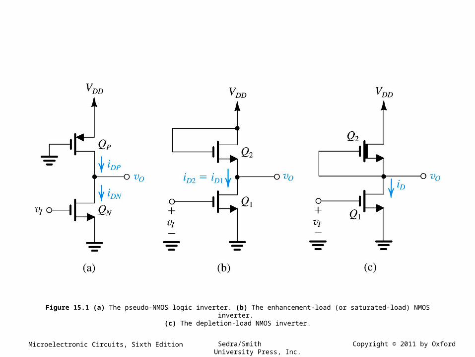
Figure 15.1 (a) The pseudo-NMOS logic inverter. (b) The enhancement-load (or saturated-load) NMOS inverter. (c) The depletion-load NMOS inverter.
3
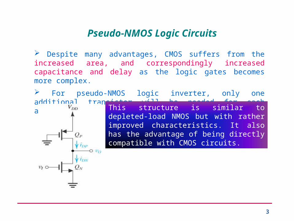
Pseudo-NMOS Logic Circuits
Despite many advantages, CMOS suffers from the increased area, and correspondingly increased capacitance and delay as the logic gates becomes more complex.
For pseudo-NMOS logic inverter, only one additional transistor will be needed for each additional gate input.
This structure is similar to depleted-load NMOS but with rather improved characteristics. It also has the advantage of being directly compatible with CMOS circuits.

4
Static Operation of A Pseudo-NMOS Logic Inverter (1)
The obvious disadvantage of the inverter is the non-zero VOL for VI=VDD (point E). It causes the static power dissipation to be PD= Isat X VDD.
These 2 parameters approach zero for conventional CMOS inverter.
Figure 15.2 Graphical construction to determine the VTC of the inverter in Fig. 15.1(a).

5
Static Operation of A Pseudo-NMOS Logic Inverter (2)
VTC for the pseudo-NMOS inverter.
Figure 15.3 VTC for the pseudo-NMOS inverter. This curve is plotted for VDD = 5
V, Vtn = −Vtp = 1 V, and r = 9.

6
Static Operation of A Pseudo-NMOS Logic Inverter (3)
Important parameters of the pseudo-NMOS inverter.
The larger the value of r, the lower VOL is and the wider the noise margins are. However, the larger r increases the asymmetry in the dynamic response and makes the gate larger for a given (W/L)P.
Ratioed (Pseudo-NMOS) vs. Ratioless (complementary CMOS) logic circuit.

7
Dynamic Operation of A Pseudo-NMOS Logic Inverter
The tPHL and tPLH of the pseudo-NMOS inverter are
The approximation establishes for a large value of r
Since kp is r times smaller than kn, tPLH will be r times larger than tPHL. Thus the circuit exhibits an asymmetrical delay performance.

8
Gate Circuit of A Pseudo-NMOS Logic
4-input pseudo-NMOS NOR and NAND gates are shown below. Note that each requires only 5 transistors compared to 8 used in complementary CMOS.
NOR type consumes less area than NAND type. Pseudo-NMOS is suited for applications in which the output remains high most of the time.
Figure 15.4 NOR and NAND gates of the pseudo-NMOS type.

9
Pass-Transistor Logic Circuits (1)
A simple approach for implementing logic functions utilizes series and parallel combinations of switches that are controlled by input variables to connect the input and output nodes.
Each of the switches can be implemented either by a single NMOS transistor or by a pair of CMOS transistors connected in CMOS transmission gate configuration.
CMOS transmission gate
Y=AC
Figure 15.5 Conceptual pass-transistor logic gates. (a) Two switches, controlled by the input variables B and C, when connected in series in the path between the input node to which an input variable A is applied and the output node (with an implied load to ground) realize the
function Y = ABC. (b) When the two switches are connected in parallel, the function realized is Y = A(B + C).
Figure 15.6 Two possible implementations of a voltage-controlled switch connecting nodes A and Y: (a) single NMOS transistor and (b) CMOS transmission gate.

10
Pass-Transistor Logic Circuits (2)
An essential requirement in the design of pass-transistor logic is ensuring that every circuit node has at all times a low-resistance path to VDD or to ground.
If B is high, S1 closes and Y=A.
Y will be VDD if A is high or ground if A is low.
If B is low, S1 opens and Y becomes a high-impedance node.
If voltage of Y is initially zero, it will remain so.
If voltage of Y is initially high at VDD, then the inevitable leakage current will discharge the C and can no longer be considered a static circuit.
Figure 15.7 A basic design requirement of PTL circuits is that every node have, at all times, a low resistancepath to either ground or VDD. Such a path does not exist in (a) when B is low and S1 is open. It is provided in
(b) through switch S2.

11
Pass-Transistor Logic Circuits (3)
The problem can be easily solved by establishing for node Y a low-resistance path that is activated when B goes low.
Another switch, S2, controlled by B is connected between Y and ground. When B goes low, S2 closes and establishes a low-resistance path between Y and ground.
Figure 15.7 A basic design requirement of PTL circuits is that every node have, at all times, a low resistancepath to either ground or VDD. Such a path does not exist in (a) when B is low and S1 is open. It is provided in
(b) through switch S2.
12
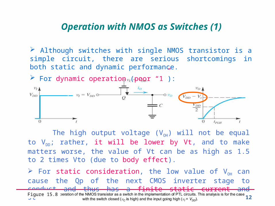
Operation with NMOS as Switches (1)
Although switches with single NMOS transistor is a simple circuit, there are serious shortcomings in both static and dynamic performance.
For dynamic operation (poor “1”):
The high output voltage (VOH) will not be equal to VDD; rather, it will be lower by Vt, and to make matters worse, the value of Vt can be as high as 1.5 to 2 times Vto (due to body effect).
For static consideration, the low value of VOH can cause the Qp of the next CMOS inverter stage to conduct and thus has a finite static current and static power dissipation.
Figure 15.8

13
Operation with NMOS as Switches (2)
Operation of the NMOS switch as the input goes low is shown below.
It results in a “good 0”. Note that the drain of an NMOS transistor is always higher in voltage than the source; correspondingly, the drain and source terminals interchange roles in comparison to previous case.

14
Operation with NMOS as Switches (3)
2 methods are proposed to solve the aforementioned signal-level loss (VOH=VDD-Vt) problem.
Circuit–based technology.
Process technology. If the Vt can be reduced, the signal-level loss would become less significant. Device with Vt=0 is known as natural device.
If vO1 is high but not equal to VDD
vO2 is low
QR turns on
supplying a current to charge C to VDD.
This arrangement of QR is somewhat involved since it creates the “positive-feedback” loop around the CMOS inverter. Fortunately, it is the “weak PMOS”.
Figure 15.10 The use of transistor QR, connected in a feedback loop around the CMOS inverter, to restore the VOH level, produced by Q1, to VDD.

Microelectronic Circuits, Sixth Edition Sedra/Smith Copyright © 2011 by Oxford University Press, Inc.
Figure 15.11 The CMOS transmission gate and its circuit symbol.

Microelectronic Circuits, Sixth Edition Sedra/Smith Copyright © 2011 by Oxford University Press, Inc.
Figure 14.12 Operation of the transmission gate as a switch in PTL circuits with (a) vI high and (b) vI low.Figure 15.12

17
Operation with CMOS Transmission Gate as Switches (1)
Great improvement in static and dynamic performance are obtained when the switches are implemented with CMOS transmission gate.
Qn will stop conducting when vo= VDD-Vtn
Qp will enter triode region at vo= |Vtp|, but will continue to conduct until C is fully charged and vo= VDD.
Qp provides the gate with a good “1”. tPLH will be lower than that in the case of single NMOS switch
due to additional current available from Qp. Additional Qp, however, adds the value of C.

18
Operation with CMOS Transmission Gate as Switches (2)
With vI goes from high to low, the output waveform is shown below.
Qp will cease conduction when vo falls to |Vtp|.
Qn, however, will continue to conduct until C is fully discharged and vo = VOL = 0V.
The transmission gates provide far superior performance than single NMOS switches. The price paid is increased circuit complexity, area and capacitance.

Microelectronic Circuits, Sixth Edition Sedra/Smith Copyright © 2011 by Oxford University Press, Inc.

Microelectronic Circuits, Sixth Edition Sedra/Smith Copyright © 2011 by Oxford University Press, Inc.
Figure 15.14 (a) A transmission gate connects the output of a CMOS inverter to the input of another. (b) Equivalent circuit for the purpose
of analyzing the propagation delay of the circuit in (a).
Microelectronic Circuits, Sixth Edition Sedra/Smith Copyright © 2011 by Oxford University Press, Inc.
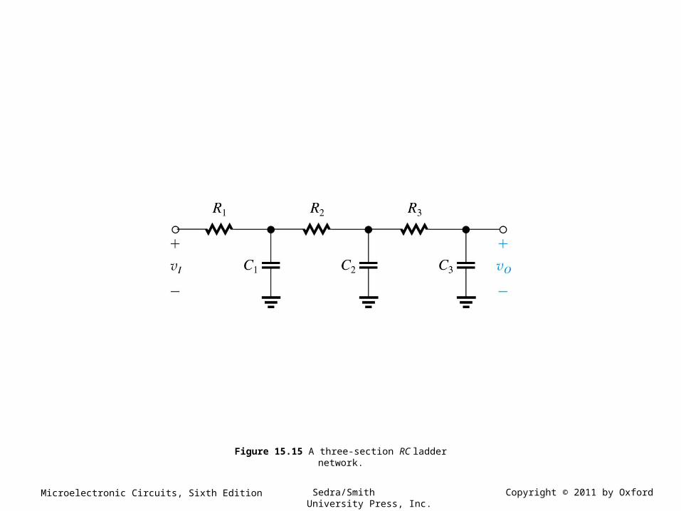
Figure 15.15 A three-section RC ladder network.

22
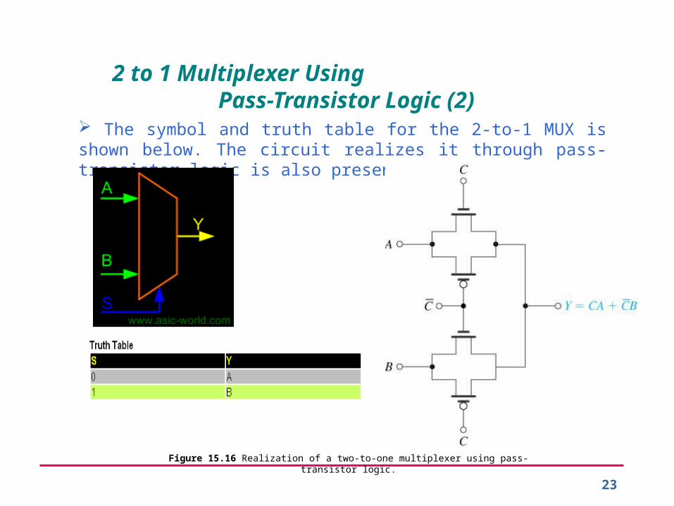
2 to 1 Multiplexer Using Pass-Transistor Logic (1)
A multiplexer (MUX) is a digital switches which connects data from one of n sources to the output. A number of select inputs determine which data source is connected to the output.
23
2 to 1 Multiplexer Using Pass-Transistor Logic (2)
The symbol and truth table for the 2-to-1 MUX is shown below. The circuit realizes it through pass-transistor logic is also presented.
Figure 15.16 Realization of a two-to-one multiplexer using pass-transistor logic.

24
Exclusive-OR Realization Using Pass-Transistor Logic
Only 8 transistors (4 for inverter and 4 for transmission gates) are required for XOR realization.
Note that 12 transistors are needed by using complementary CMOS.
12 transistors8 transistors
Figure 15.17 Realization of the XOR function using pass-transistor logic.

Microelectronic Circuits, Sixth Edition Sedra/Smith Copyright © 2011 by Oxford University Press, Inc.
Figure 15.18 An example of a pass-transistor logic gate utilizing both the input variables and their complements. This type of circuit is therefore known as complementary pass-transistor logic, or CPL. Note that both the output function and its complement are generated.
An example of a pass-transistor logic gate utilizing both the input variables and their complements. This type of circuit is therefore known as complementary pass-transistor logic or CPL. Note that both the output function and its complement are generated.
Complementary Pass-Transistor Logic

26
Dynamic MOS Logic Circuits
The logic circuits we have studied thus far are of the static type. That is, every node has a low resistance path to VDD or ground (the voltage of each node is well defined at all times). No node is left floating. Dynamic logic circuits rely on the storage of signal voltages on parasitic capacitance at certain nodes. It needs to be periodically refreshed; thus the clock with specified minimum frequency is essential.
Features of various logic-circuit styles we have studied. Complementary CMOS: pros easy to design, strong noise immunity, no static power,
equal propagation delay in both directions. cons requirement of 2 transistors for each additional gate input. Pseudo-NMOS: It reduces the number of required transistors at the
expense of static power dissipation. Pass-transistor logic: It requires the use of complementary inverters to
restore signal level. Dynamic logic: It maintains the low device count of Pseudo-NMOS
while reducing the static power to zero.
27
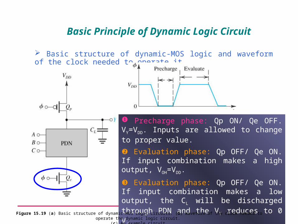
Basic Principle of Dynamic Logic Circuit
Basic structure of dynamic-MOS logic and waveform of the clock needed to operate it.
Precharge phase: Qp ON/ Qe OFF. VY=VDD. Inputs are allowed to change to proper value.
Evaluation phase: Qp OFF/ Qe ON. If input combination makes a high output, VOH=VDD.
Evaluation phase: Qp OFF/ Qe ON. If input combination makes a low output, the CL will be discharged through PDN and the VY reduces to 0 V.
Figure 15.19 (a) Basic structure of dynamic-MOS logic circuits. (b) Waveform of the clock needed to operate the dynamic logic circuit. (c) An example circuit.

28
An Example of Dynamic Logic Circuit
Sizing of the PDN transistors often follows the same procedure employed in the design of static CMOS.
For Qp, we select a W/L ratio large enough to ensure that CL will be fully charged during precharge interval. The size of Qp should be small so that CL will not be increased.
Figure 15.19 (a) Basic structure of dynamic-MOS logic circuits. (b) Waveform of the clock needed to operate the dynamic logic circuit. (c) An example circuit.

Microelectronic Circuits, Sixth Edition Sedra/Smith Copyright © 2011 by Oxford University Press, Inc.
Figure 15.20 Circuits for Example 15.3.

30
Non-Ideal Effects (1)
4 major sources of non-ideal operation of dynamic logic circuits are: Noise margins:
since VIL~VIH~Vtn, NML=Vtn; NMH=VDD-Vtn
The noise margins are far from equal and NML is rather low. Output voltage decay due to leakage effects:
Without a path to ground through the PDN, the output voltage will remain high at VDD. In practice, leakage current will cause CL to discharge and the main source of such leakage is the reversed-biased junction leakage current (double for every 10oC).
The circuit will malfunction if the clock is operating at a very low frequency and the output is not refreshed periodically.
reversed-biased junction leakage current
31
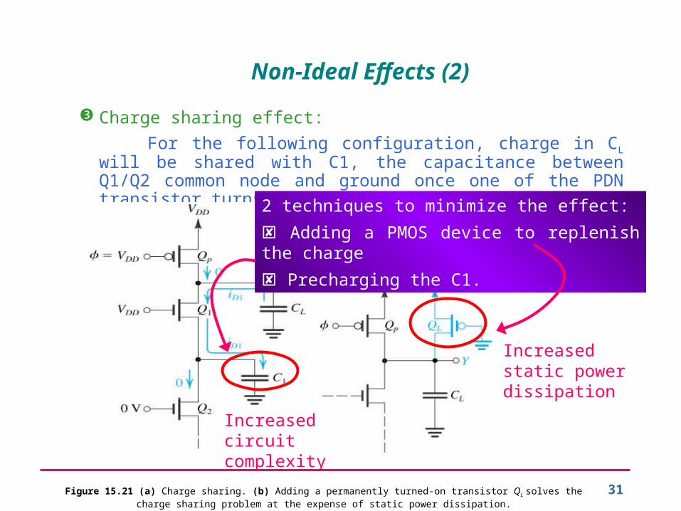
Non-Ideal Effects (2)
Charge sharing effect:
For the following configuration, charge in CL will be shared with C1, the capacitance between Q1/Q2 common node and ground once one of the PDN transistor turns on.
2 techniques to minimize the effect:
Adding a PMOS device to replenish the charge
Precharging the C1.
Increased static power dissipation
Increased circuit complexity
Figure 15.21 (a) Charge sharing. (b) Adding a permanently turned-on transistor QL solves the charge sharing problem at the expense of static power dissipation.
32
Non-Ideal Effects (3)
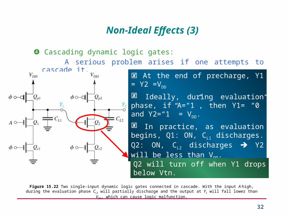
Cascading dynamic logic gates: A serious problem arises if one attempts to cascade it.
At the end of precharge, Y1 = Y2 =VDD
Ideally, during evaluation phase, if A=“1”, then Y1= “0” and Y2=“1” = VDD.
In practice, as evaluation begins, Q1: ON, CL1 discharges. Q2: ON, CL2 discharges Y2 will be less than VDD.
Q2 will turn off when Y1 drops below Vtn.
Figure 15.22 Two single-input dynamic logic gates connected in cascade. With the input A high, during the evaluation phase CL2 will partially discharge and the output at Y2 will fall lower than VDD, which can cause logic malfunction.

Microelectronic Circuits, Sixth Edition Sedra/Smith Copyright © 2011 by Oxford University Press, Inc.
Figure E 15.10

34
Non-Ideal Effects (4)
Domino CMOS logic gates: The aforementioned problem when cascading the logics can be
solved by the Domino CMOS logic gate.
2 single-input Domino CMOS logic gates connected in cascade.
Figure 15.23 The Domino CMOS logic gate. The circuit consists of a dynamic-MOS logic gate with a static-CMOS inverter connected to the output. During evaluation, Y either will remain low (at 0 V) or will make one 0-to-1 transition (to VDD).
35
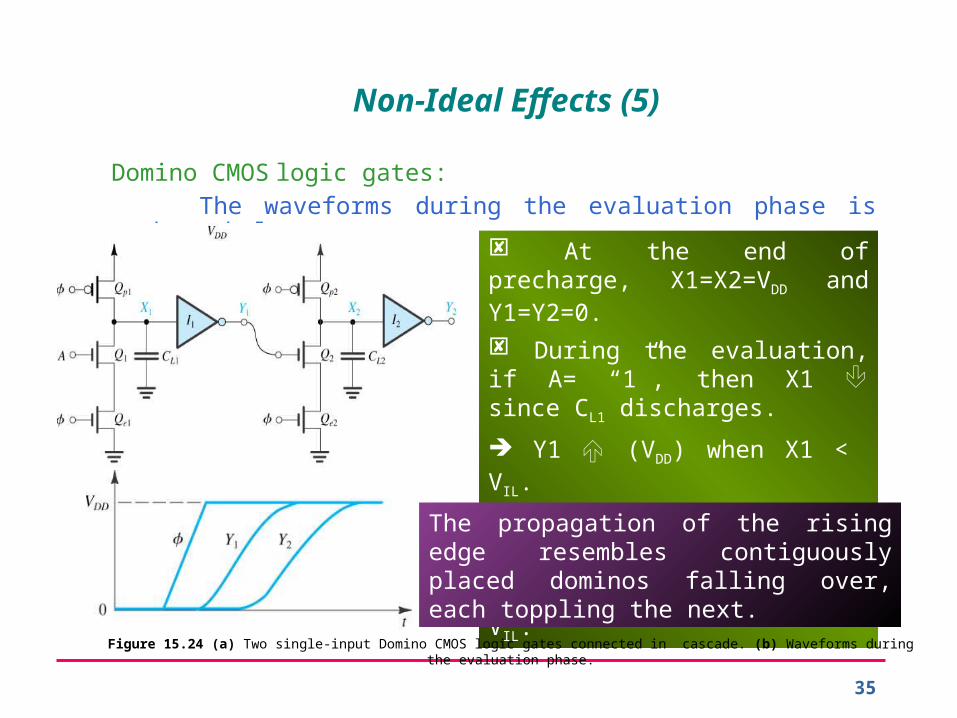
Non-Ideal Effects (5)
Domino CMOS logic gates: The waveforms during the evaluation phase is shown below.
At the end of precharge, X1=X2=VDD and Y1=Y2=0.
During the evaluation, if A= “1”, then X1 since CL1 discharges.
Y1 (VDD) when X1 < VIL.
X2 since CL2 discharges.
Y2 (VDD) when X2 < VIL.
The propagation of the rising edge resembles contiguously placed dominos falling over, each toppling the next.
Figure 15.24 (a) Two single-input Domino CMOS logic gates connected in cascade. (b) Waveforms during the evaluation phase.

36
Emitter-Coupled Logic –(1)
The high speed is achieved by operating all transistors out of saturation to avoid storage time delays. In addition, the logic swing signal swings relatively small (~0.8V) to reduce the charging and discharging time.
When vI is greater than VR by about 4 VT vO1 = VCC –I x RC
vO2 = VCC.
When vI is smaller than VR by about 4 VT vO1 = VCC
vO2 = VCC –I x RC
Figure 15.25 The basic element of ECL is the differential pair. Here, VR is a reference voltage.

37
Emitter-Coupled Logic –(2)
Important features of ECL: The differential nature of the circuit makes it less susceptible to picked-up noise.
The current drawn from the power supply remains constant during switching which produces no current spikes.
The output signal levels are both referenced to VCC and can be made particularly stable with VCC = 0V.
Some means has to be provided to make the output signal levels compatible with those at the input so that one gate can drive another.
The availability of complementary output considerably simplifies logic design with ECL.

38
Emitter-Coupled Logic –(3)
ECL Families: ECL 100K: tp ~ 0.75 ns and PD ~ 40 mW DP = 30 pJ.
ECL 10K : tp ~ 2 ns and PD ~ 25 mW DP = 50 pJ. Slightly slower than ECL 100K but is easier to use. Rise and fall times are deliberately made longer (edge speed 3.5
ns for ECL 10K vs. 1 ns for ECL 100K) to reduce signal coupling. A variant of ECL has become popular in VLSI applications.

Microelectronic Circuits, Sixth Edition Sedra/Smith Copyright © 2011 by Oxford University Press, Inc.
Figure E15.12
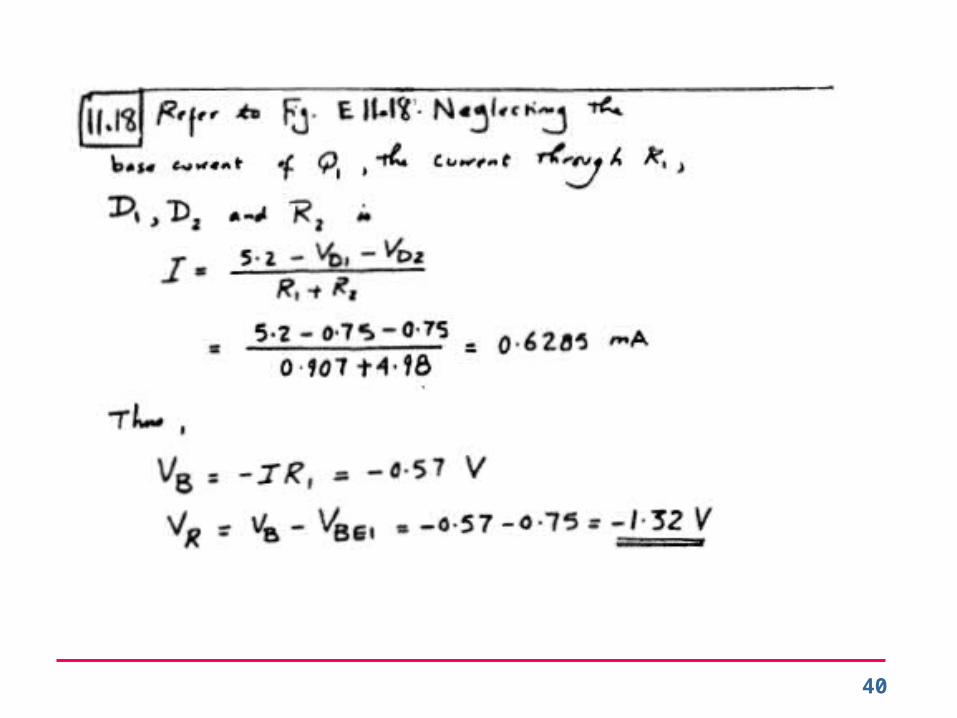
40

Microelectronic Circuits, Sixth Edition Sedra/Smith Copyright © 2011 by Oxford University Press, Inc.
Figure 15.26 Basic circuit of the ECL 10K logic-gate family.
42
Emitter-Coupled Logic –(5)
The bias network. The network generates a reference voltage VR of –1.32V at room temperature. VR is made to change with temperature in a predetermined manner so as to keep the noise margins almost constant.
VR is also made relatively insensitive to variations in the power supply voltage VEE.
Differential input stage Paralleling input transistors (QA and QB) are used to implement OR and NOR functions. Current in RE remains approximately constant over the normal range of operation. Resistances are used to connect each input terminal to the negative supply can leave unused inputs open.

43
Emitter-Coupled Logic –(6)
Emitter-follower output On-chip loads are not included since that gate drives a transmission line terminated at the other end in most of high-speed logic.
Emitter followers shift the level by one vBE drop the shifted levels are centered around VR.
Provide low output resistance and large current driving capability. Use of separate power-supply prevents the coupling of power-supply spikes from the output circuit to the gate circuit.
Figure 15.27 The proper way to connect high-speed logic gates such as ECL. Properly terminating the transmission line connecting the two gates eliminates the “ringing” that would otherwise corrupt the logic signals. (See Section 15.4.6.)
Microelectronic Circuits, Sixth Edition Sedra/Smith Copyright © 2011 by Oxford University Press, Inc.
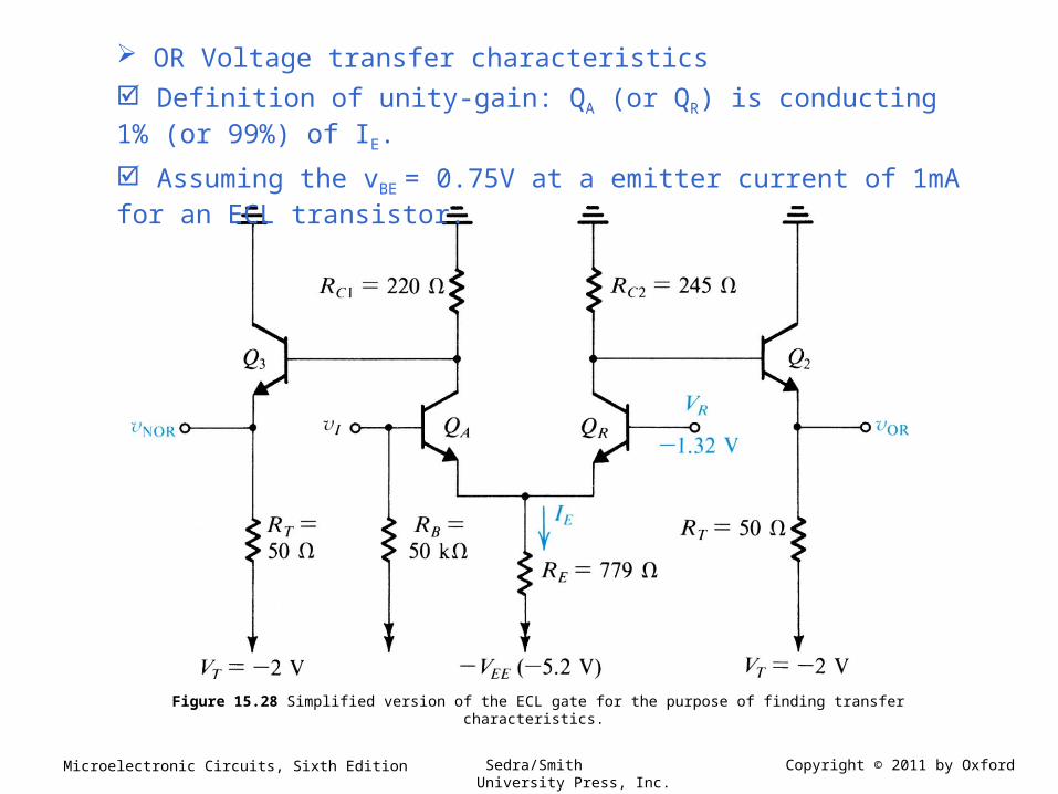
Figure 15.28 Simplified version of the ECL gate for the purpose of finding transfer characteristics.
OR Voltage transfer characteristics
Definition of unity-gain: QA (or QR) is conducting 1% (or 99%) of IE.
Assuming the vBE = 0.75V at a emitter current of 1mA for an ECL transistor.

45
Emitter-Coupled Logic –(8)
OR Voltage transfer characteristics.
Figure 15.30 Circuit for determining VOH.
Microelectronic Circuits, Sixth Edition Sedra/Smith Copyright © 2011 by Oxford University Press, Inc.
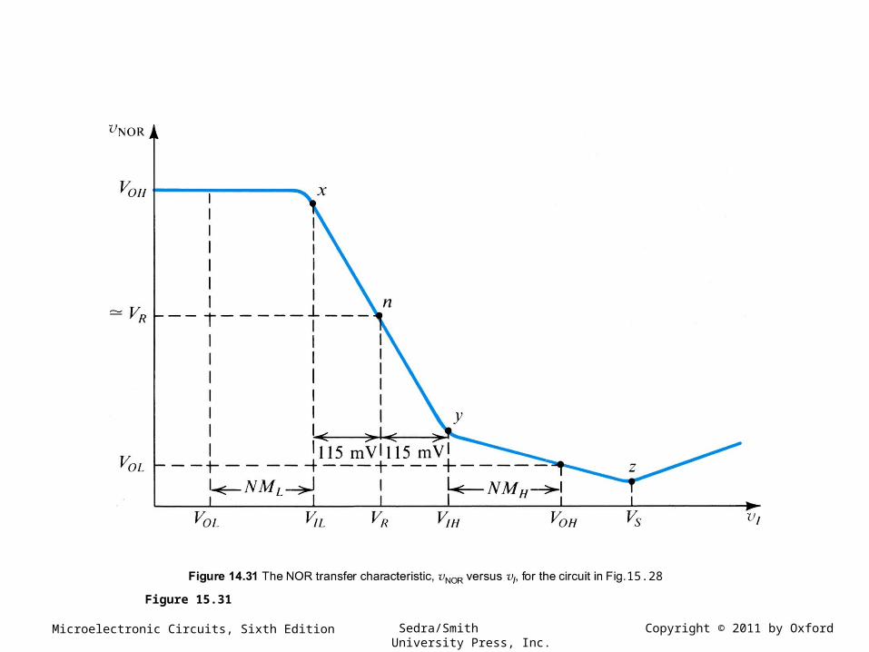
Figure 15.31
15.28

47
Emitter-Coupled Logic –(9)
NOR Voltage transfer characteristics.
Figure 15.31

48
Emitter-Coupled Logic –(10)
Circuit for finding, vNOR versus vI for the range vI > VIH.
vI > VIH, QA operates in the active mode.
At point z, QA saturates. Further increments in vI cause the collector voltage to increase.
Figure 15.32
49
Emitter-Coupled Logic –(11)
Manufacturers’ Specifications
VILmax: -1.475 V VIHmin = -1.105 V
VOLmax: -1.630V VOHmin = -0.980V
Fan-Out
IIL = (-1.77+5.2)/50 = 69μA; IIH = (-0.88+5.2)/50 + 4/101 = 126μA
Input currents are small and output resistance is small
fan-out of ECL is not limited by logic-level. The fan-out is limited by considerations of circuit speed. Speed The speed is measured by the delay of its basic gate and by the rise and fall time of the output waveforms. The ECL gate shows shorter rise time than its fall time by using emitter follower as the output stage.
50
Emitter-Coupled Logic –(12)
Signal Transmission ECL is particularly sensitive to ringing because the signal levels are so small. One solution is to keep the wires very “short” with respect to the signal rise/fall time the reflections return while the input is still rising/falling. If greater lengths are needed, then transmission lines must be used the reflection is suppressed with proper termination.

Microelectronic Circuits, Sixth Edition Sedra/Smith Copyright © 2011 by Oxford University Press, Inc.
Figure 15.33 Equivalent circuit for determining the temperature coefficient of the reference voltage VR.
Microelectronic Circuits, Sixth Edition Sedra/Smith Copyright © 2011 by Oxford University Press, Inc.
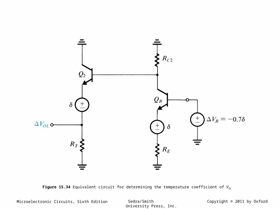
Figure 15.34 Equivalent circuit for determining the temperature coefficient of VOL

Microelectronic Circuits, Sixth Edition Sedra/Smith Copyright © 2011 by Oxford University Press, Inc.
Figure 15.35 Equivalent circuit for determining the temperature coefficient of VOH.

54
Emitter-Coupled Logic –(13)
Wired-OR Capability The emitter follower output stage of the ECL family allows wired-OR for logic design. The OR function is implemented by wiring the output of several gates in parallel.
The applications of ECL include supercomputers, as well as high speed and high frequency communication system.
Figure 15.36 The wired-OR capability of ECL.

Microelectronic Circuits, Sixth Edition Sedra/Smith Copyright © 2011 by Oxford University Press, Inc.
Figure 15.37 Development of the BiCMOS inverter circuit. (a) The basic concept is to use an additional bipolar transistor to increase the output current drive of each of QN and QP of the CMOS inverter. (b) The circuit in (a) can be thought of as utilizing these composite devices.
(c) To reduce the turn-off times of Q1 and Q2, “bleeder resistors” R1 and R2 are added. (d) Implementation of the circuit in (c) using NMOS transistors to realize the resistors. (e) An improved version of the circuit in (c) obtained by connecting the lower end of R1 to the output node.

Microelectronic Circuits, Sixth Edition Sedra/Smith Copyright © 2011 by Oxford University Press, Inc.
Figure 15.38 Equivalent circuits for charging and discharging a load capacitance C. Note that C includes all the capacitances present at the output node.

Microelectronic Circuits, Sixth Edition Sedra/Smith Copyright © 2011 by Oxford University Press, Inc.
Figure 15.39 A BiCMOS two-input NAND gate.
Related Documents