LM5180 GNDB LDO 10 F GND1 MUX SN74LV4052A TX1 RX1 TX1 RX1 Backplane ASIC LDO TPS7A47 ¤™$’& ADS122U04 TX1 RX1 ISO7721 TPS26625 eFuse 25 mA + OVP GND1 AVDD DVDD GND1 GND1 GNDB V1+ = 25V GND1 Burden TPS26625 eFuse 25 mA + OVP GND2 10 F Vout4 AIN4 Vout1 AIN1 LDO TPS7A47 ¤™$’& ADS122U04 TX1 RX1 ISO7721 AVDD DVDD GND2 GND2 GNDB TX4 UART Burden REF REF GNDB GNDB VIN 4-20 mA Loop 4-20 mA Loop 3.3 V GNDB GND 10 μF UART GND2 TR1/1 RX4 TR1/4 1 TIDUEN8 – April 2019 Submit Documentation Feedback Copyright © 2019, Texas Instruments Incorporated Channel-to-Channel Isolated Analog Input Module Reference Design Design Guide: TIDA-010048 Channel-to-Channel Isolated Analog Input Module Reference Design Description This reference design is a four channel-to-channel, isolated 4–20 mA, current-loop analog input module. The design includes a short circuit, overcurrent, and overvoltage limit function for condition monitoring sensor and module applications. The major features of this analog input module include channel isolation, a multi-channel analog input module powered up by a single flyback converter using TI´s LM5180 device, a power supply to 2-wire transmitter and short-circuit protection circuit. This design can also support a four- channel analog input module. Resources TIDA-010048 Design Folder LM5180 Product Folder ADS122U04 Product Folder TPS2662 Product Folder ISO7721 Product Folder TPS7A47 Product Folder TVS3300 Product Folder SN74LV4052A Product Folder ASK Our E2E™ Experts Features • 1 to 4 channel-to-channel isolated analog input module. • Supply for field transmitters with output power limitation (short limited to 25mA) • Transmitter supply: 25 ±1V, IOUT < 25-mA peak • Input protected against miswiring • UART interface 24b ΔΣADC to reduce BOM size and cost Applications • Mixed module (AI,AO,DI,DO) • Analog input module An IMPORTANT NOTICE at the end of this TI reference design addresses authorized use, intellectual property matters and other important disclaimers and information.

Welcome message from author
This document is posted to help you gain knowledge. Please leave a comment to let me know what you think about it! Share it to your friends and learn new things together.
Transcript

LM5180
GNDB LDO
10 �F
GND1
MUXSN74LV4052A
TX1
RX1
TX1
RX1Backplane
ASIC
LDOTPS7A47
¨�$'& ADS122U04
TX1
RX1ISO7721
TPS26625eFuse
25 mA +OVP
GND1
AVDD DVDD
GND1GND1
GNDB
V1+ = 25V
GND1
Burden
TPS26625eFuse
25 mA +OVP
GND2
10 �F
Vout4
AIN4
Vout1
AIN1
LDOTPS7A47
¨�$'& ADS122U04
TX1
RX1ISO7721
AVDD DVDD
GND2GND2GNDB
TX4
UART
BurdenREF
REF
GNDB GNDB
VIN 4-20 mALoop
4-20 mALoop
3.3 VGNDB
GND10 µF
UART
GND2
TR1/1
RX4
TR1/4
1TIDUEN8–April 2019Submit Documentation Feedback
Copyright © 2019, Texas Instruments Incorporated
Channel-to-Channel Isolated Analog Input Module Reference Design
Design Guide: TIDA-010048Channel-to-Channel Isolated Analog Input ModuleReference Design
DescriptionThis reference design is a four channel-to-channel,isolated 4–20 mA, current-loop analog input module.The design includes a short circuit, overcurrent, andovervoltage limit function for condition monitoringsensor and module applications. The major features ofthis analog input module include channel isolation, amulti-channel analog input module powered up by asingle flyback converter using TI´s LM5180 device, apower supply to 2-wire transmitter and short-circuitprotection circuit. This design can also support a four-channel analog input module.
Resources
TIDA-010048 Design FolderLM5180 Product FolderADS122U04 Product FolderTPS2662 Product FolderISO7721 Product FolderTPS7A47 Product FolderTVS3300 Product FolderSN74LV4052A Product Folder
ASK Our E2E™ Experts
Features• 1 to 4 channel-to-channel isolated analog input
module.• Supply for field transmitters with output power
limitation (short limited to 25mA)• Transmitter supply: 25 ±1V, IOUT < 25-mA peak• Input protected against miswiring• UART interface 24b ΔΣADC to reduce BOM size
and cost
Applications• Mixed module (AI,AO,DI,DO)• Analog input module
An IMPORTANT NOTICE at the end of this TI reference design addresses authorized use, intellectual property matters and otherimportant disclaimers and information.

Field Transmitter(Two-Wire Analog Output)
Supply
CurrentOutput
TIDA-010048
Efuse
ADCDigital
IsoDigitalOutput
TVS
VOUTSupply
Current Flow
AIN
System Description www.ti.com
2 TIDUEN8–April 2019Submit Documentation Feedback
Copyright © 2019, Texas Instruments Incorporated
Channel-to-Channel Isolated Analog Input Module Reference Design
1 System DescriptionThe TIDA-010048 universal analog input module is four channel-to-channel isolated with short-circuitprotection, over-current limit, overvoltage limit and high-performance design. Analog input modulesdigitalize temperature, current (4–20 mA) and voltage (±10V). Analog input modules are challenged withincreasing channel density, tolerating high common mode voltages, high throughput with low power,functional or intrinsic safety, high dynamic range, EMI and miswiring protection. This design implements atwo-wire 4–20 mA current-loop analog input module system. The design supports remote sensortransmitters without an additional power supply which can eliminate the external ground pin on the casingso the field engineer can avoid miswiring problems. It also can support four-channel analog input modulewith a single flyback converter. This means the PLC side can reduce the cost and BOM size and achievechannel-to-channel isolated analog input module system. Figure 1 shows the typical two-wire current-loopsystem. The supply of the field transmitter is provided by the analog input module side and current outputof field transmitter transfer the analog signal back to analog input module side. There is another keycharacteristic of this design which uses the eFuse to prevent the overcurrent and overvoltagesimultaneously to limit the power flow into the field side.
Figure 1. Typical Two-Wire Current-Loop System
1.1 Key System Specifications
Table 1. Key System Specifications
PARAMETER SPECIFICATIONSNumber of analog input channels (2-wire transmitters) Four Channels
Power supply part for 2-wire transmitter perchannel
Supply voltage 25 VDCOvervoltage limit 33 VDCOvercurrent and short-circuit limit 25 mA
IsolationBetween backplane and analog input channels 1000 VAC, 1 minuteBetween analog input channels 1000VAC, 1 minute
Analog input module for current loop perchannel
Range 4–20 mAResolution 24-bitInternal PGA Gain 1, 2Sampling Cycle 20 SPS to 1000 SPS
Form factorEach Channel 5.2 cm × 1.8 cmEntire board 9.5 cm × 8.4 cm
Operating temperature –400C to 850C

LM5180
GNDB LDO
10 �F
GND1
MUXSN74LV4052A
TX1
RX1
TX1
RX1Backplane
ASIC
LDOTPS7A47
¨�$'& ADS122U04
TX1
RX1ISO7721
TPS26625eFuse
25 mA +OVP
GND1
AVDD DVDD
GND1GND1
GNDB
V1+ = 25V
GND1
Burden
TPS26625eFuse
25 mA +OVP
GND2
10 �F
Vout4
AIN4
Vout1
AIN1
LDOTPS7A47
¨�$'& ADS122U04
TX1
RX1ISO7721
AVDD DVDD
GND2GND2GNDB
TX4
UART
BurdenREF
REF
GNDB GNDB
VIN 4-20 mALoop
4-20 mALoop
3.3 VGNDB
GND10 µF
UART
GND2
TR1/1
RX4
TR1/4
www.ti.com System Overview
3TIDUEN8–April 2019Submit Documentation Feedback
Copyright © 2019, Texas Instruments Incorporated
Channel-to-Channel Isolated Analog Input Module Reference Design
2 System Overview
2.1 Block Diagram
Figure 2. System Block Diagram

System Overview www.ti.com
4 TIDUEN8–April 2019Submit Documentation Feedback
Copyright © 2019, Texas Instruments Incorporated
Channel-to-Channel Isolated Analog Input Module Reference Design
2.2 Design ConsiderationsThe block diagram in Figure 2 is separated into three parts: isolated power, analog front end, and digitalisolation signal readout circuit.
The isolated power is mainly implemented with TI’s flyback converter (LM5180). The transformer usesWurth Electronics to customize the transformer which can achieve one-four channel isolated power. Thecurrent limit on every channel is set into 25 mA at 25 V DC which is enough for field transmitterapplications. The isolation level is decided by the transformer which is functional insulation. The ratedvoltage of this transformer can be up to 1000 VAC for one minute. If a higher level of isolation is required,the transformer design can be changed to meet the specification. VIN and VOUT voltage are equal to 25 V.The current limit and voltage threshold of every channel which is decided by the eFuse set up at 25 mAand 33 V. Every isolated maximum channel power can provide the field side to 1.25 W.
The analog front end circuit implements a 4–20 mA current loop by the ADS122U04 device which usesthe UART interface and a 24-bit ∆∑ADC. It could reduce the channel number of digital isolator and theBOM size and cost. The power of ADC is supplied by the wide VIN LDO (TPS7A47). Using the wide VINLDO can reduce the additional buck converter for stepping down voltage and retains ADC performance. Ifthere are other analog input requirements such as voltage ±10 V, 0–5 V, 0–10 V; Current ±25 mA, 0–20mA; temperature input RTD, thermocouple and thermistor, see the following TI reference design.
The designers can choose a dual-channel digital isolator for signal isolation due to UART ADC. It canreduce the silicon package size and total BOM cost. A dual four-channel analog MUX in the PLC sidehelps the customer choose the necessary analog input module to measure the analog signal which candecrease the pins of UART interface on the microcontroller in the backplane side. This provides moreflexibility in analog input module system design.
2.3 Highlighted Products
2.3.1 LM5180The LM5180 device is a primary-side regulated (PSR) flyback converter with high efficiency over a wideinput voltage range of 4.5 V to 65 V. The isolated output voltage is sampled from the primary-side flybackvoltage, eliminating the need for an optocoupler, voltage reference, or third winding from the transformerfor output voltage regulation.
2.3.2 ADS122U04The ADS122U04 device is a high precision, 24-bit, analog-to-digital converter (ADC) that offers integratedPGA, reference, and internal fault monitors. The device features two differential or four single-endedinputs through a flexible input multiplexer (MUX). The device data rates can be up to 2000 samples-per-second (SPS) with single-cycle settling. At 20 SPS, the digital filter offers simultaneous 50-Hz and 60-Hzrejection for noisy industrial applications. The internal PGA offers gains up to 128. The ADS122U04features a 2-wire, UART-compatible interface. With a UART interface, engineers only need a two-channeldigital isolator. It could reduce the cost and BOM size.

www.ti.com System Overview
5TIDUEN8–April 2019Submit Documentation Feedback
Copyright © 2019, Texas Instruments Incorporated
Channel-to-Channel Isolated Analog Input Module Reference Design
2.3.3 TPS26625The TPS2662X family have a wide supply input range of 4.5 V to 57 V. The device can withstand andprotect the loads from positive and negative supply voltages to ±60 V. TPS26625 devices support bothinput as well as output reverse polarity protection features. Load, source, and device protection areprovided with many adjustable features including overcurrent, output slew rate and overvoltage,undervoltage thresholds. Therefore, using a single eFuse circuit can achieve power limit functions for fieldtransmitter in hazardous region.
2.3.4 TPS7A47The TPS7A470x is a family of positive voltage (+36 V), ultra-low noise (4 µVRMS) low-dropout linearregulators (LDO) capable of sourcing a 1-A load. The TPS7A47 device is designed with bipolartechnology, high-precision instrumentation applications where clean voltage rails are critical to maximizesystem performance. This feature makes the device ideal for powering operational amplifiers, analog-to-digital converters (ADCs), digital-to-analog converters (DACs), and other high-performance analogcircuitry in critical applications such as medical, radio frequency (RF), and test-and-measurement.
2.3.5 TVS3300The TVS3300 is a protection device with a very low leakage current component. It also can robustly shuntup to 35 A of IEC 61000-4-5 fault current to protect systems from high-power transients or lightningstrikes. The device offers a solution to the common industrial signal line EMC requirement to survive up to1-kV IEC 61000-4-5 open circuit voltage coupled through a 42-Ω impedance.
2.3.6 ISO7721The ISO772X devices are high-performance, dual-channel digital isolators with 5000 VRMS (DW and DWVpackages) and 3000 VRMS (D package) isolation ratings per UL 1577. These devices are also certified byVDE, TUV, CSA, and CQC. The ISO7721 device has both channels in the opposite direction; therefore, italso could support UART interface.
2.3.7 SN74LV4052AThe SN74LV4052A device is a dual, 4-channel multiplexer and demultiplexer that is designed for 2-V to5.5-V VCC operation. The dual 4-channel MUX can help to choose the necessary analog input module tomeasure analog signal.
16
11
9
144
3
2
1
6
5
8
7
PRI18 ± 60VDC
220 ± 350 kHz
SEC25VDC, 60mADC
SEC25VDC, 60mADC
SEC25VDC, 60mADC
SEC25VDC, 60mADC
System Overview www.ti.com
6 TIDUEN8–April 2019Submit Documentation Feedback
Copyright © 2019, Texas Instruments Incorporated
Channel-to-Channel Isolated Analog Input Module Reference Design
2.4 System Design Theory
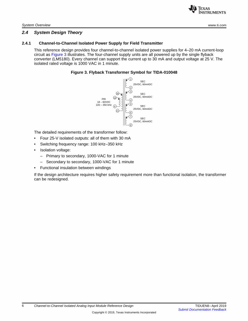
2.4.1 Channel-to-Channel Isolated Power Supply for Field TransmitterThis reference design provides four channel-to-channel isolated power supplies for 4–20 mA current-loopcircuit as Figure 3 illustrates. The four-channel supply units are all powered up by the single flybackconverter (LM5180). Every channel can support the current up to 30 mA and output voltage at 25 V. Theisolated rated voltage is 1000 VAC in 1 minute.
Figure 3. Flyback Transformer Symbol for TIDA-010048
The detailed requirements of the transformer follow:• Four 25-V isolated outputs: all of them with 30 mA• Switching frequency range: 100 kHz–350 kHz• Isolation voltage:
– Primary to secondary, 1000-VAC for 1 minute– Secondary to secondary, 1000-VAC for 1 minute
• Functional insulation between windings
If the design architecture requires higher safety requirement more than functional isolation, the transformercan be redesigned.

VCC11
INA7
OUTB6
GND25
GND14
INB3
OUTA2
VCC28
ISO7721DWV
U5AIN0
9
AIN18
AIN25
AIN34
AVDD10
AVSS3
DGND2
DVDD11
GPIO016
GPIO115
GPIO2/DRDY12
REFN6
REFP7
RX14
TX13
RESET1
PAD17
ADS122U04IRTER
U4
10V0.1uF
C9
10V0.1uF
C10
AIN2,3 and REFX will be openGND
4.70k
R8
4.70k
R11
50V0.01uF
C750V1000pF
C6
50V1000pF
C8
AIN
GND
47k
R9
GND BGND
ADC_RX
ADC_TX
BVCC
GND
AIN
From ADS122u04 EVM
24.9R10
D3RB751S40
LED1
LED2
0
R12
0
R13
DVDD
DVDDAVDD
10V0.1uF
C11
10V0.1uF
C12
FLT
SW1
FB2
VIN3
EN/UVLO4
SS/BIAS5
TC6
RSET7
GND8
PAD9
LM5180QNGURQ1
U1
1
3
5
8
4
2
7
6
9
11
14
16
T1
750317963
100V2.2uF
C5536k
R1
255kRtc1
12.1k
Rset1
126kR2
Schotcky Diode for RectifierPeak repetitive revearse voltage=60v
Output Current=2AZener Diode for clamp limit
Zener voltage=28v
D8CMDD4448
BGND
50V0.022uF
C6
VIN
iso_power1
iso_power2
iso_power3
iso_power4
GND1
GND2
GND3
GND4
TP1
1573-2
TP2
1573-2
100kR3
28V
D5MMSZ5255B-7-F
D2
RB168LAM150TR
V1+
50V4.7uF
C1
28V
D1MMSZ5255B-7-F
GND1
D4
RB168LAM150TR
V2+
50V4.7uF
C2
28V
D3MMSZ5255B-7-F
GND2
D7
RB168LAM150TR
V3+
50V4.7uF
C3
28V
D6MMSZ5255B-7-F
GND3
D10
RB168LAM150TR
V4+
50V4.7uF
C4
28V
D9MMSZ5255B-7-F
GND4
www.ti.com System Overview
7TIDUEN8–April 2019Submit Documentation Feedback
Copyright © 2019, Texas Instruments Incorporated
Channel-to-Channel Isolated Analog Input Module Reference Design
Figure 4. Channel-to-Channel Isolated Power Supply Using LM5180
2.4.2 Analog Front EndThe module features a two-wire, four channel, 4–20 mA analog input module which can be used withsensor transmitters with 4–20 mA current loop. The main purpose of this circuit is to build a reliabledelivery of 4–20 mA loop current analog input front end. Figure 5 shows the detail of the analog front endcircuit. R10 is the Rshunt to transfer the current signal into voltage. A first-order resistor-capacitor (RC) filteris used in the AFE. The filter corner frequency is set at 1.6 kHz. D3 is for shifting the input signal level. Itcan make the analog input signal remain in full-scale range of the ADC when the PGA is on. The ADCusing a UART interface can reduce the number channels of digital isolator.
Figure 5. Analog Input Front End
2.4.3 Data Accquistion Systems Using UART InterfaceIn the Reducing System Cost, Size and Power Consumption in Isolated Data Acquisition Systems UsingADS122U04 Tech Note, the ADS122U04 replaces the standard SPI interface with a 2-wire UARTinterface. Engineers only need a twochannel digital isolator with no additional uC or processor in the ADCside which is depicted in Figure 6. Using TI’s ADS122U04 device, the industry’s first sensor measurementADC with UART interface, designers can reduce their digital isolator power consumption and cost by >30% compared to conventional implementations while still taking advantage of the high resolution andintegration of a 24-bit delta-sigma ADC. To build the data acquisition systems for four sets of analog inputmodules, the design uses the dual four-channel MUX to capture the required data from different analoginput module as Figure 6 shows.

Repeat(iso_power)
Repeat(ADC_TX)
Repeat(ADC_RX)
BVCC
Repeat(GND)
BGND
Repeat(CH,1,4)TIDACB-0039_Analog Input Module.SchDoc
2Y01
2Y22
2-COM3
2Y34
2Y15
INH6
GND7
GND8
B9
A10
1Y311
1Y012
1-COM13
1Y114
1Y215
VCC16
SN74LV4052A
U7
BVCC
BGND
ADC_RX1
ADC_RX2
ADC_RX3
ADC_RX4
ADC_TX1
ADC_TX2
ADC_TX3
ADC_TX4
ADC_RX
ADC_TX
iso_power
GNDGPO1
GPO2
MC
UT
XM
CU
RX
0
R19
0
R20
0
R21
0
R22
0
R23
0
R24
0
R25 BGND
BVCC
System Overview www.ti.com
8 TIDUEN8–April 2019Submit Documentation Feedback
Copyright © 2019, Texas Instruments Incorporated
Channel-to-Channel Isolated Analog Input Module Reference Design
Figure 6. Data Acquisition Systems Using UART Interface Block Diagram
2.4.4 Two-Wire 4–20 mA Current-Loop Analog Input ModuleFigure 1 shows a typical two-wire, 4–20 mA current-loop analog input module which TIDA-010048 isbased on. The key advantage of the two-wire system can provide 4–20 mA power for the field transmitter.Therefore, the whole field side system does not need an extra power supply to power-up the fieldtransmitter. Another advantage is to avoid setting the grounding pin outside the casing of analog inputmodule, so you can use TVS to connect the power supply and the analog input pin to protect the surge asthe Typical Application section in the TVS3300 33-V Flat-Clamp Surge Protection Device Data Sheetdetails.

Output Current (mA)
Effi
cien
cy (
%)
4 5 6 7 8 9 10 11 12 13 14 15 16 17 18 19 2074
75
76
77
78
79
80
D001
CH1CH2CH3CH4
Source Measure Unit
± +CH1
Source Measure Unit
± + CH2
Oscilloscope
VIN
GNDBVOUT1,4
GND1,4
www.ti.com Test and Measurement Results
9TIDUEN8–April 2019Submit Documentation Feedback
Copyright © 2019, Texas Instruments Incorporated
Channel-to-Channel Isolated Analog Input Module Reference Design
3 Test and Measurement Results
3.1 Power Tree Test ResultFigure 7 shows the power tree test setup. Use the source measure unit to get the flyback efficiency, crossregulation, start-up waveform, and the waveform of ripple when the load variation is in the other channel.Because the actual performance data may be affected by measurement techniques and environmentalvariables, these curves and waveforms are presented for reference and may differ from actual fieldmeasurements.
Figure 7. Power Tree Test Setup
3.1.1 Efficiency PerformanceThe efficiency measurements were taken channel by channel as Figure 8 shows. The efficiencyperformance is as expected. Table 2 shows the whole system performance. It includes the powerdissipation of other channels quiescent current loss and the power loss of the signal chain circuit.Although, it is a little lower than ideal, it is still enough for the power dissipation of the field transmitter.
Figure 8. Efficiency Performance of Flyback
Table 2. Total System Efficiency
4 mA FOR EACHCHANNEL
12 mA FOR EACHCHANNEL
20 mA FOR EACHCHANNEL
Input power (W) 0.763 1.65 2.65Output power (W) 0.413 1.27 2.12Total efficiency (%) 54.1 77.3 79.9

Test and Measurement Results www.ti.com
10 TIDUEN8–April 2019Submit Documentation Feedback
Copyright © 2019, Texas Instruments Incorporated
Channel-to-Channel Isolated Analog Input Module Reference Design
3.1.2 Start-Up WaveformFigure 9 shows the start-up waveform. The waveform is tested at full load at 25-V input. The four channelsets at the same output load and input situation. The default internal soft-start time of the LM5180 deviceis 6 ms and an externally-programmable soft start.
Figure 9. Start-Up Waveform
3.1.3 Load Regulation and Cross RegulationFigure 10 shows the influence at the output of flyback with the other channel load varying from 4 mA to 20mA. The green line and the blue line, respectively, represent the load state of the load variation channeland the constant 20-mA channel under load variation conditions. The normal channel of VOUT variation isabout 22.4 mV. The load variation channel of VOUT variation is about 94 mV.
Figure 10. Load Regulation Waveform

Load(%)
V+
(Vol
tage
)
20 35 50 65 80 9525
25.05
25.1
25.15
25.2
25.25
25.3
D002
CH1CH2
CH3CH4
www.ti.com Test and Measurement Results
11TIDUEN8–April 2019Submit Documentation Feedback
Copyright © 2019, Texas Instruments Incorporated
Channel-to-Channel Isolated Analog Input Module Reference Design
Figure 11 shows the cross regulation performance of the reference design. The flyback output voltage isinfluenced by the load current of the other channels. The variation of the output voltage level is fairlystable under all conditions in the 4–20 mA load current and the reasons of voltage gap between CH1,2and CH3,4 is mostly related with transformer parameter differences.
Figure 11. Cross Regulation Performance
3.2 Test Result of Overcurrent and Short-Circuit ProtectionThe eFuse provides the short-circuit and overcurrent limit protection feature for two-wire current loop.Figure 12 illustrates the behavior of the system during output short-circuit condition. The short-circuitbehavior induces about 42-mV overvoltage in VOUT in the normal channel. Figure 12 also shows the auto-retry function and the retry time per cycle is 512 ms.
Figure 12. eFuse Short-Circuit Protection Waveform
Figure 2 shows the VOUT pin of the normal and short channel and the FLT pin. The voltage of the Faultpin goes down after the short-circuit occurs. It could provide the alert signal to the controller side, if theshort circuit happens.
This reference design has an eFuse in the power line which can provide the overvoltage and overcurrentprotection simultaneously. If the field transmitter is located in a hazardous region, any sparks or blinkcreate the high possibility of explosion. Due to that, the eFuse can provide the power limit for the fieldtransmitter side, it is suitable for safety applications. Table 3 shows voltage, current, and power limit ofevery channel.

> @
N
22
Noise Free bits log Effective 2.72 bitsstddev samples 6.6
§ ·� �¨ ¸¨ ¸u© ¹
> @
N
22
Effective bits logstddev samples
§ · ¨ ¸¨ ¸
© ¹
INT,REFcodecode
2.048V23N 1
4 20mABURDEN
2 2I
R 24.9
uu�
�
§ ·§ ·¨ ¸¨ ¸
¨ ¸¨ ¸¨ ¸¨ ¸
© ¹ © ¹
Source Measure Unit
± +
PCUSB to UART
AIN1,4
GND1,4
Power Supply
± +
VIN
GNDB
RT
S
VC
C
GN
DC
TS
RX
DT
XD
Test and Measurement Results www.ti.com
12 TIDUEN8–April 2019Submit Documentation Feedback
Copyright © 2019, Texas Instruments Incorporated
Channel-to-Channel Isolated Analog Input Module Reference Design
Table 3. Power Limit by eFuse
CH1 CH2 CH3 CH4Overvoltage limit 33.3 V 33.3 V 33.3 V 33.2 VOvercurrent limit 24.944 mA 25.174 mA 25.311 mA 25.574 mAOver power limit 830 mW 839 mW 843 mW 849 mW
3.3 Test Result of Analog Input Module PerformanceFigure 13 shows the signal chain test setup. Due to the UART interface signal chain design, testing theADC performance is easier. Using the STDI, connect the PC and the board directly to reduce the numberof isolation channels and the current consumption. The 4–20 mA analog input current source used is thehigh precision SMU (B2912A) which is accurate up to 0.02% in the 10-mA range. It ensures the realperformance of the ADC is measured. To obtain the effective and noise-free bits, the standard deviation iscalculated from 750 samples taken from an externally-applied 4-mA, 12-mA, and 20-mA constant current.The loop current is not measured by an external DMM since the absolute value is not of importance.Figure 14 through Figure 25 show the relatively current data histogram based on Figure 13 at differentconditions.
Figure 13. Signal Chain Test Setup
(1)
The effective number of bits and noise-free bits are calculated using Equation 2 and Equation 3:
where• N = data width of converter (2)
(3)

ADC Conversion Current Error (nA)
Num
ber
of O
ccur
renc
es
0
20
40
60
80
100
120
140
160
-700 -600 -500 -400 -300 -200 -100 0 100 200 300 400 500 600 700
D003D007 ADC Conversion Current Error (nA)
Num
ber
of O
ccur
renc
es
0
50
100
150
200
250
-6k -5k -4k -3k 3k -2k -1k 0 1k 2k 3k 4k 5k
D003D008
ADC Conversion Current Error (nA)
Num
ber
of O
ccur
renc
es
0
20
40
60
80
100
120
140
160
-700 -600 -500 -400 -300 -200 -100 0 100 200 300 400 500 600
D003D005 ADC Conversion Current Error (nA)
Num
ber
of O
ccur
renc
es
0
50
100
150
200
250
-6k -5k -4k -3k 3k -2k -1k 0 1k 2k 3k 4k 5k
D006D006
ADC Conversion Current Error (nA)
Num
ber
of O
ccur
renc
es
0
20
40
60
80
100
120
140
160
-700 -600 -500 -400 -300 -200 -100 0 100 200 300 400 500 600
D003D003 ADC Conversion Current Error (nA)
Num
ber
of O
ccur
renc
es
0
50
100
150
200
250
-6k -5k -4k -3k 3k -2k -1k 0 1k 2k 3k 4k 5k
D004
www.ti.com Test and Measurement Results
13TIDUEN8–April 2019Submit Documentation Feedback
Copyright © 2019, Texas Instruments Incorporated
Channel-to-Channel Isolated Analog Input Module Reference Design
Figure 14. Histogram – 4 mA, Gain = 1, SPS = 20, STD = 21.61ENOB = 19.56
Figure 15. Histogram – 4 mA, Gain = 1, SPS = 1000, STD =183.84 ENOB = 16.47
Figure 16. Histogram – 4 mA, Gain = 2, SPS = 20, STD = 21.8ENOB = 19.55
Figure 17. Histogram – 4 mA, Gain = 2, SPS = 1000, STD =149.64 ENOB = 16.77
Figure 18. Histogram – 12 mA, Gain = 1, SPS = 20, STD = 24.4ENOB = 19.39
Figure 19. Histogram – 12 mA, Gain = 1, SPS = 1000, STD =152.7 ENOB = 16.75

( )RMS effective bits
Full scale range
GainRMS noise V
2
-æ öç ÷è øm =
ADC Conversion Current Error (nA)
Num
ber
of O
ccur
renc
es
0
10
20
30
40
50
60
70
80
90
100
-700 -600 -500 -400 -300 -200 -100 0 100 200 300 400 500 600 -800 -900 700 800 900 1000 1100D003D013D013
ADC Conversion Current Error (nA)
Num
ber
of O
ccur
renc
es
0
10
20
30
40
50
60
70
80
90
100
-700 -600 -500 -400 -300 -200 -100 0 100 200 300 400 500 600 -800 -900 700 800 900 1000 1100D003D013D013
ADC Conversion Current Error (nA)
Num
ber
of O
ccur
renc
es
0
50
100
150
200
250
-6k -5k -4k -3k 3k -2k -1k 0 1k 2k 3k 4k 5k
D003D012D012ADC Conversion Current Error (nA)
Num
ber
of O
ccur
renc
es
0
20
40
60
80
100
120
140
-700 -600 -500 -400 -300 -200 -100 0 100 200 300 400 500 600 700 800 -800 -900D003D011
ADC Conversion Current Error (nA)
Num
ber
of O
ccur
renc
es
0
20
40
60
80
100
120
140
160
180
200
-6k -5k -4k -3k 3k -2k -1k 0 1k 2k 4k 5k
D003D010ADC Conversion Current Error (nA)
Num
ber
of O
ccur
renc
es
0
20
40
60
80
100
120
140
-700 -600 -500 -400 -300 -200 -100 0 100 200 300 400 500 600 -800 -900 700 800D003D009
Test and Measurement Results www.ti.com
14 TIDUEN8–April 2019Submit Documentation Feedback
Copyright © 2019, Texas Instruments Incorporated
Channel-to-Channel Isolated Analog Input Module Reference Design
Figure 20. Histogram – 12 mA, Gain = 2, SPS = 20, STD = 31.25ENOB = 19.03
Figure 21. Histogram – 12 mA, Gain = 2, SPS = 1000, STD =177.51 ENOB = 16.53
Figure 22. Histogram – 20 mA, Gain = 1, SPS = 20, STD = 25.43ENOB = 19.33
Figure 23. Histogram – 20 mA, Gain = 1, SPS = 1000, STD =150.07 ENOB = 16.77
Figure 24. Histogram – 20 mA, Gain = 2, SPS = 20, STD = 35.07ENOB = 18.87
Figure 25. Histogram – 20 mA, Gain = 2, SPS = 1000, STD =168.73 ENOB = 16.60
With the obtained effective bits and noise-free bits, the input referred noise can be calculated by taking therange of the input range (dependent on gain) into account (Equation 4 and Equation 5). The full-scalerange is –2.5 V to 2.5 V = 5 V.
(4)
� �PP noise free bits
Full scale rangeGain
Peak noise V2 �
�§ ·¨ ¸© ¹P
www.ti.com Test and Measurement Results
15TIDUEN8–April 2019Submit Documentation Feedback
Copyright © 2019, Texas Instruments Incorporated
Channel-to-Channel Isolated Analog Input Module Reference Design
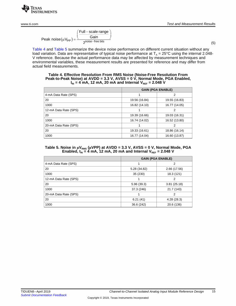
(5)
Table 4 and Table 5 summarize the device noise performance on different current situation without anyload variation. Data are representative of typical noise performance at TA = 25°C using the internal 2.048-V reference. Because the actual performance data may be affected by measurement techniques andenvironmental variables, these measurement results are presented for reference and may differ fromactual field measurements.
Table 4. Effective Resolution From RMS Noise (Noise-Free Resolution FromPeak-to-Peak Noise) at AVDD = 3.3 V, AVSS = 0 V, Normal Mode, PGA Enabled,
IIN = 4 mA, 12 mA, 20 mA and Internal VREF = 2.048 V
GAIN (PGA ENABLE)4-mA Data Rate (SPS) 1 220 19.56 (16.84) 19.55 (16.83)1000 16.82 (14.10) 16.77 (14.05)12-mA Data Rate (SPS) 1 220 19.39 (16.66) 19.03 (16.31)1000 16.74 (14.02) 16.52 (13.80)20-mA Data Rate (SPS) 1 220 19.33 (16.61) 18.86 (16.14)1000 16.77 (14.04) 16.60 (13.87)
Table 5. Noise in μVRMS (μVPP) at AVDD = 3.3 V, AVSS = 0 V, Normal Mode, PGAEnabled, IIN = 4 mA, 12 mA, 20 mA and Internal VREF = 2.048 V
GAIN (PGA ENABLE)4-mA Data Rate (SPS) 1 220 5.28 (34.82) 2.66 (17.56)1000 35 (230) 18.3 (121)12-mA Data Rate (SPS) 1 220 5.96 (39.3) 3.81 (25.18)1000 37.3 (246) 21.7 (143)20-mA Data Rate (SPS) 1 220 6.21 (41) 4.28 (28.3)1000 36.6 (242) 20.6 (136)

ADC Conversion Current Error (nA)
Num
ber
of O
ccur
renc
es
0
20
40
60
80
100
120
140
160
180
200
-6k -5k -4k -3k 3k -2k -1k 0 1k 2k 3k 4k 5k
D003D020ADC Conversion Current Error (nA)
Num
ber
of O
ccur
renc
es
0
20
40
60
80
100
120
140
160
-700 -600 -500 -400 -300 -200 -100 0 100 200 300 400 500 600 700 800 -800 -900D003D019D019
ADC Conversion Current Error (nA)
Num
ber
of O
ccur
renc
es
0
20
40
60
80
100
120
140
160
180
200
-6k -5k -4k -3k 3k -2k -1k 0 1k 2k 3k 4k 5k
D003D018ADC Conversion Current Error (nA)
Num
ber
of O
ccur
renc
es
0
20
40
60
80
100
120
140
-700 -600 -500 -400 -300 -200 -100 0 100 200 300 400 500 600 700 800D003D017D017
ADC Conversion Current Error (nA)
Num
ber
of O
ccur
renc
es
0
20
40
60
80
100
120
140
160
180
-700 -600 -500 -400 -300 -200 -100 0 100 200 300 400 500 600
D003D015 ADC Conversion Current Error (nA)
Num
ber
of O
ccur
renc
es
0
50
100
150
200
250
-6k -5k -4k -3k 3k -2k -1k 0 1k 2k 3k 4k 5k
D003D016D016
Test and Measurement Results www.ti.com
16 TIDUEN8–April 2019Submit Documentation Feedback
Copyright © 2019, Texas Instruments Incorporated
Channel-to-Channel Isolated Analog Input Module Reference Design
This reference design measures the noise performance in load transient (4 mA to 20 mA). Figure 26through Figure 31 show the noise performance of ADC. Table 6 through Table 9 show the detailed results.As the tables show, the overvoltage does not significantly affect the overall ADC performance, due to wideVIN LDO with high PSRR.
Figure 26. Histogram – 4 mA, Gain = 1, SPS = 20, STD = 20.96ENOB = 19.61
Figure 27. Histogram – 4 mA, Gain = 1, SPS = 1000, STD =141.87 ENOB = 16.85
Figure 28. Histogram – 12 mA, Gain = 1, SPS = 20, STD = 25.24ENOB = 19.34
Figure 29. Histogram – 12 mA, Gain = 1, SPS = 1000, STD =163 ENOB = 16.65
Figure 30. Histogram – 20 mA, Gain = 1, SPS = 20, STD = 24.02ENOB = 19.41
Figure 31. Histogram – 20 mA, Gain = 1, SPS = 20, STD =161.22 ENOB = 16.67

www.ti.com Test and Measurement Results
17TIDUEN8–April 2019Submit Documentation Feedback
Copyright © 2019, Texas Instruments Incorporated
Channel-to-Channel Isolated Analog Input Module Reference Design
Table 6. Effective Resolution From RMS Noise (Noise-Free Resolution FromPeak-to-Peak Noise) at AVDD = 3.3 V, AVSS = 0 V, Normal Mode, PGA Enabled,IIN = 4 mA, 12 mA, 20 mA and Internal VREF = 2.048 V, Load Variation From 4–20
mA
GAIN (PGA ENABLE)4-mA Data Rate (SPS) 120 19.61 (16.89)1000 16.85 (14.13)12-mA Data Rate (SPS) 120 19.34 (16.62)1000 16.65 (13.93)20-mA Data Rate (SPS) 120 19.41 (16.69)1000 16.67 (13.94)
Table 7. Noise in μVRMS (μVPP) at AVDD = 3.3 V, AVSS = 0 V, Normal Mode, PGAEnabled, IIN = 4 mA, 12 mA, 20 mA and Internal VREF = 2.048 V, Load Variation
From 4–20 mA
GAIN (PGA ENABLE)4-mA Data Rate (SPS) 120 5.12 (33.8)1000 34.6 (229)12-mA Data Rate (SPS) 120 6.16 (40.7)1000 39.8 (263)20-mA Data Rate (SPS) 120 5.87 (38.7)1000 39.4 (260)
Table 8. Effective Resolution From RMS Noise (Noise-Free Resolution FromPeak-to-Peak Noise) at AVDD = 3.3 V, AVSS = 0 V, Normal Mode, PGA Enabled,
IIN = 4 mA, 12 mA, 20 mA and Internal VREF = 2.048 V, Short Circuit
4-mA Data Rate (SPS) = 20 Gain (PGA enable) = 119.61 (16.89)
12-mA Data Rate (SPS) = 20 Gain (PGA enable) = 119.34 (16.62)
20-mA Data Rate (SPS) = 20 Gain (PGA enable) = 119.41 (16.69)
Table 9. Noise in μVRMS (μVPP) at AVDD = 3.3 V, AVSS = 0 V, Normal Mode, PGAEnabled, IIN = 4 mA, 12 mA, 20 mA and Internal VREF = 2.048 V, Short Circuit
4-mA Data Rate (SPS) = 20 Gain (PGA enable) = 15.39 (31.47)
12-mA Data Rate (SPS) = 20 Gain (PGA enable) = 15.91 (31.26)
20-mA Data Rate (SPS) = 20 Gain (PGA enable) = 15.77 (31.32)

Design Files www.ti.com
18 TIDUEN8–April 2019Submit Documentation Feedback
Copyright © 2019, Texas Instruments Incorporated
Channel-to-Channel Isolated Analog Input Module Reference Design
4 Design Files
4.1 SchematicsTo download the schematics, see the design files at TIDA-010048.
4.2 Bill of MaterialsTo download the bill of materials (BOM), see the design files at TIDA-010048.
4.3 Altium ProjectTo download the Altium Designer® project files, see the design files at TIDA-010048.
4.4 Gerber FilesTo download the Gerber files, see the design files at TIDA-010048.
4.5 Assembly DrawingsTo download the assembly drawings, see the design files at TIDA-010048.
5 Software FilesTo download the software files, see the design files at TIDA-010048.
6 Related Documentation1. Texas Instruments, Reducing System Cost, Size and Power Consumption in Isolated Data Acquisition
Systems Using ADS122U04 Tech Note2. Texas Instruments, TVS3300 33-V Flat-Clamp Surge Protection Device Data Sheet3. Texas Instruments, LM5180 65-VIN PSR Flyback DC/DC Converter With 100-V, 1.5-A Integrated Power
MOSFET4. Texas Instruments, ADS122U04 24-Bit, 4-Channel, 2-kSPS, Delta-Sigma ADC With UART Interface
Data Sheet5. Texas Instruments, TPS2662x 60-V, 800-mA Industrial eFuse With Integrated Input and Output
Reverse Polarity Protection Data Sheet6. Texas Instruments, ISO772x High-Speed, Robust EMC, Reinforced Dual-Channel Digital Isolators
Data Sheet7. Texas Instruments, TPS7A470x 36-V, 1-A, 4-µVRMS, RF LDO Voltage Regulator Data Sheet8. Texas Instruments, TVS3300 33-V Flat-Clamp Surge Protection Device Data Sheet9. Texas Instruments, SN74LV4052A Dual 4-Channel Analog Multiplexers and Demultiplexers Data
Sheet

www.ti.com Related Documentation
19TIDUEN8–April 2019Submit Documentation Feedback
Copyright © 2019, Texas Instruments Incorporated
Channel-to-Channel Isolated Analog Input Module Reference Design
6.1 TrademarksE2E is a trademark of Texas Instruments.Altium Designer is a registered trademark of Altium LLC or its affiliated companies.All other trademarks are the property of their respective owners.
6.2 Third-Party Products DisclaimerTI'S PUBLICATION OF INFORMATION REGARDING THIRD-PARTY PRODUCTS OR SERVICES DOESNOT CONSTITUTE AN ENDORSEMENT REGARDING THE SUITABILITY OF SUCH PRODUCTS ORSERVICES OR A WARRANTY, REPRESENTATION OR ENDORSEMENT OF SUCH PRODUCTS ORSERVICES, EITHER ALONE OR IN COMBINATION WITH ANY TI PRODUCT OR SERVICE.
7 About the AuthorBEN SU is a Field Application Engineer at Texas Instruments. Ben has mixed-signal IC design experiencein TSMC fabrication and focused on wireless power IC and SAR ADC during his study career. Ben earnedhis masters degree in electrical engineering from National Chiao Tung University in Hsinchu, Taiwan.

IMPORTANT NOTICE AND DISCLAIMER
TI PROVIDES TECHNICAL AND RELIABILITY DATA (INCLUDING DATASHEETS), DESIGN RESOURCES (INCLUDING REFERENCEDESIGNS), APPLICATION OR OTHER DESIGN ADVICE, WEB TOOLS, SAFETY INFORMATION, AND OTHER RESOURCES “AS IS”AND WITH ALL FAULTS, AND DISCLAIMS ALL WARRANTIES, EXPRESS AND IMPLIED, INCLUDING WITHOUT LIMITATION ANYIMPLIED WARRANTIES OF MERCHANTABILITY, FITNESS FOR A PARTICULAR PURPOSE OR NON-INFRINGEMENT OF THIRDPARTY INTELLECTUAL PROPERTY RIGHTS.These resources are intended for skilled developers designing with TI products. You are solely responsible for (1) selecting the appropriateTI products for your application, (2) designing, validating and testing your application, and (3) ensuring your application meets applicablestandards, and any other safety, security, or other requirements. These resources are subject to change without notice. TI grants youpermission to use these resources only for development of an application that uses the TI products described in the resource. Otherreproduction and display of these resources is prohibited. No license is granted to any other TI intellectual property right or to any thirdparty intellectual property right. TI disclaims responsibility for, and you will fully indemnify TI and its representatives against, any claims,damages, costs, losses, and liabilities arising out of your use of these resources.TI’s products are provided subject to TI’s Terms of Sale (www.ti.com/legal/termsofsale.html) or other applicable terms available either onti.com or provided in conjunction with such TI products. TI’s provision of these resources does not expand or otherwise alter TI’s applicablewarranties or warranty disclaimers for TI products.
Mailing Address: Texas Instruments, Post Office Box 655303, Dallas, Texas 75265Copyright © 2019, Texas Instruments Incorporated
Related Documents


![Channel Isolated Analog-Digital Converter Module/Channel ...€¦ · A - 2 [Installation Precautions] CAUTION Use the programmable controller in an environment that meets the general](https://static.cupdf.com/doc/110x72/5f86134ed223da77bc75feb2/channel-isolated-analog-digital-converter-modulechannel-a-2-installation.jpg)