FD‐SOI Technology Benefits for Variation‐aware SRAM design Changhwan Shin Department of Electrical Engineering and Computer Sciences University of California, Berkeley, CA USA Acknowledgements Prof. Tsu‐Jae King Liu, Prof. Borivoje Nikolić, Dr. Horacio Mendez, Dr. Bich‐Yen Nguyen and Dr. Carlos Mazuré FDSOI Workshop, 28 April 2011

Welcome message from author
This document is posted to help you gain knowledge. Please leave a comment to let me know what you think about it! Share it to your friends and learn new things together.
Transcript
FD‐SOI Technology Benefitsfor Variation‐aware SRAM design
Changhwan Shin
Department of Electrical Engineering and Computer SciencesUniversity of California, Berkeley, CA USA
AcknowledgementsProf. Tsu‐Jae King Liu, Prof. Borivoje Nikolić,
Dr. Horacio Mendez, Dr. Bich‐Yen Nguyen and Dr. Carlos Mazuré
FDSOI Workshop, 28 April 2011
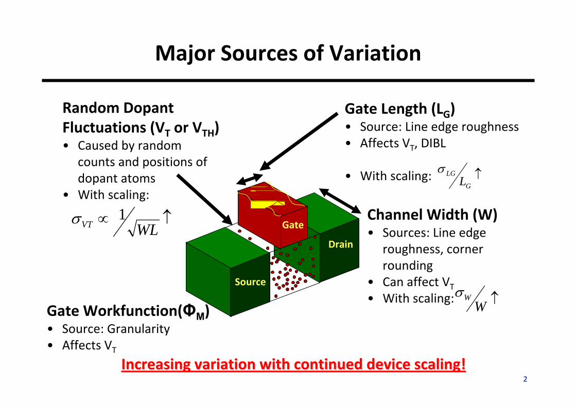
Major Sources of Variation
Drain
Gate
Source
Increasing variation with continued device scalingIncreasing variation with continued device scaling!!
Random DopantFluctuations (VT or VTH)• Caused by random
counts and positions of dopant atoms
• With scaling:
↑∝WLVT
1σ Channel Width (W)• Sources: Line edge
roughness, corner rounding
• Can affect VT
• With scaling: ↑WWσ
Gate Workfunction(ΦM)• Source: Granularity• Affects VT
2
Gate Length (LG)• Source: Line edge roughness• Affects VT, DIBL
• With scaling: ↑G
LGL
σ
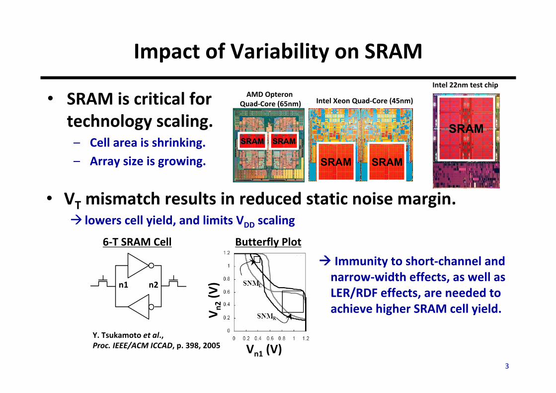
• VT mismatch results in reduced static noise margin.lowers cell yield, and limits VDD scaling
Vn1 (V)
Vn2(V)
Impact of Variability on SRAM
Y. Tsukamoto et al., Proc. IEEE/ACM ICCAD, p. 398, 2005
6‐T SRAM Cell Butterfly Plot
AMD OpteronQuad‐Core (65nm) Intel Xeon Quad‐Core (45nm)
Intel 22nm test chip
• SRAM is critical for technology scaling.– Cell area is shrinking.– Array size is growing.
Immunity to short‐channel and narrow‐width effects, as well as LER/RDF effects, are needed to achieve higher SRAM cell yield.
SRAM SRAM
SRAMSRAMSRAM
n2n1
3
Outline
• Thin‐BOX FD‐SOI Technology*– Variation‐robust device design– Variation analysis
• FDSOI SRAM Design and Comparison with Bulk Technology*
• Back‐gated Tri‐gate FD‐SOI Technology
• Summary*C. Shin et al., “Performance and area scaling benefits of FD‐SOI technology for 6‐T SRAM cells at the 22‐nm node,”IEEE Transactions on Electron Devices, Vol. 57, No. 6, pp. 1301‐1309, 2010. 4

T BOX
Raised-Drain
W SPACER
L GATE
Sub (p -doped 10 18cm-3)
T Sin+ n+
SiO 2
1020cm-3
-1020cm-3
Raised -Source
T BOX
W SPACER
LGATE
Sub (p -doped 10 18cm-3)
T Sin+
SiO 2
1020cm-3
-1020cm-3
Faceted in-situ-dopedRaised-source
Faceted in-situ-dopedRaised-drain
T S/DWS/DT BOX
Raised-Drain
W SPACER
L GATE
Sub (p -doped 10 18cm-3)
T Sin+ n+
SiO 2
1020cm-3
-1020cm-3
Raised -Source
T BOX
W SPACER
LGATE
Sub (p -doped 10 18cm-3)
T Sin+
SiO 2
1020cm-3
-1020cm-3
Faceted in-situ-dopedRaised-source
Faceted in-situ-dopedRaised-drain
T S/DWS/D
Thin‐BOX FD‐SOI MOSFET Design
Design parametersSchematic cross‐sectional view
• Thin body (TSi < Lg/4) to suppress short‐channel effects
• Raised‐source/drain (RSD) regions to reduce series resistance(formed by low‐temperature selective epitaxial growth with in‐situ doping)
• ΦM set to meet LOP off‐state leakage (IOFF) specification
• Electrical channel length (Leff) selected for maximum ION
NMOS PMOS
Lg (nm) 25 25
Tox (nm) 1 1
tSi (nm) 6 6
TBOX (nm) 10 10
ФM (eV) 4.45 4.85
Leff (nm) 35.6 30.7
= 15nm
WS/D = 72nm; TS/D = 22.6nm
Adapted from K. Cheng et al., 2009 Symp. VLSI Technology
5

Performance Comparison
DS
TH
DS
TH
DS GS TH
TH
V2VGS TH
DS s ox DS subGS TH
sat
2DSVDS GS THV0
l ox DS subGS TH
sat
V V ‐VV S
sub
(V ‐ V )WI = μ C (1 + λV ) + I (1 ‐ e )
V ‐ V2mL 1 +E L
mVV (V ‐ V ‐ )
VW= μ C (1 + λV ) + I (1 ‐ e )
V ‐ VL 1 +E L
= I (1 ‐ e )e
Analytical model fit to simulated I‐V, used to iteratively solve for DC SRAM metrics:
Optimized to maximize ION for IOFF=3nA/um, Nbody=1018 cm-3
in saturation region
in linear region
in sub‐threshold region
0.0 0.2 0.4 0.6 0.8 1.01E-9
1E-8
1E-7
1E-6
1E-5
1E-4
1E-3
I DS
(A/u
m)
VGS (V)
Model Sentaurus
200
400
600
800
1m
I DS
(uA
/um
)
ION= 581 μA/μm @ VDD=1.0V
IOFF= 3 nA/μm
SS= 81 mV/dec
VTH,LIN= 0.366 V
VTH,SAT= 0.322 V
BULK
0.0 0.2 0.4 0.6 0.8 1.01E-9
1E-8
1E-7
1E-6
1E-5
1E-4
1E-3
I DS
(A/u
m)
VGS (V)
Model Sentaurus
200
400
600
800
1m
I DS
(uA
/um
)
ION= 581 μA/μm @ VDD=1.0V
IOFF= 3 nA/μm
SS= 81 mV/dec
VTH,LIN= 0.366 V
VTH,SAT= 0.322 V
BULK
0.0 0.2 0.4 0.6 0.8 1.01E-9
1E-8
1E-7
1E-6
1E-5
1E-4
1E-3
I DS (A
/um
)
Model Sentaurus
VGS (V)
ION= 861 μA/μm @ VDD=1.0V
SS= 75 mV/dec
VTH,LIN= 0.347 V
VTH,SAT= 0.298 V
IOFF= 3 nA/μm FD‐SOI200
400
600
800
1m
I DS (u
A/u
m)
0.0 0.2 0.4 0.6 0.8 1.01E-9
1E-8
1E-7
1E-6
1E-5
1E-4
1E-3
I DS (A
/um
)
Model Sentaurus
VGS (V)
ION= 861 μA/μm @ VDD=1.0V
SS= 75 mV/dec
VTH,LIN= 0.347 V
VTH,SAT= 0.298 V
IOFF= 3 nA/μm FD‐SOI200
400
600
800
1m
I DS (u
A/u
m)
6
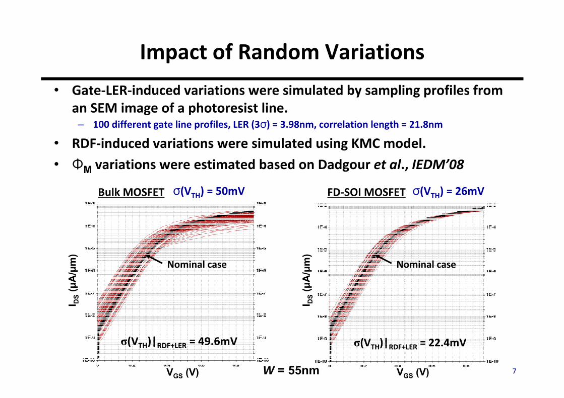
σ(VTH)|RDF+LER = 22.4mVσ(VTH)|RDF+LER = 22.4mVσ(VTH)|RDF+LER = 49.6mVσ(VTH)|RDF+LER = 49.6mV
• Gate‐LER‐induced variations were simulated by sampling profiles from an SEM image of a photoresist line.
– 100 different gate line profiles, LER (3σ) = 3.98nm, correlation length = 21.8nm
• RDF‐induced variations were simulated using KMC model.
• ΦM variations were estimated based on Dadgour et al., IEDM’08
Impact of Random Variations
Bulk MOSFET FD‐SOI MOSFET
Nominal case Nominal case
W = 55nm 7
σ(VTH) = 50mV σ(VTH) = 26mV
VGS (V) VGS (V)
I DS
(μA
/μm
)
I DS
(μA
/μm
)

Outline
• Thin‐BOX FD‐SOI Technology
• FDSOI SRAM Design and Comparison with Bulk Technology– SRAM cell design– Yield analysis
• Back‐gated Tri‐gate FD‐SOI Technology
• Summary
8

• Based on published 22nm CMOS design rules
6‐T SRAM Cell Layout
Half‐Bit Cell Layout Layout Parameters
PD
PG
PUX
YLPD
LPG
BC
WPU
D/2WPD
A/2
WPG
PD
PG
PUX
YLPD
LPG
BC
WPU
D/2WPD
A/2
WPG
Design rules SymbolSize [nm]
Cell Height
PG CH length LPG 25
PD CH length LPD 25
CONT size X 30
Gate‐to‐CONT Y 20
Total 190
Cell Width
POLY‐to‐POLY A 30
POLY‐to‐DIF ext B 20
PD Width WPD 55
N/P isolation C 50
PU width WPU 32
DIF‐DIF (min) D 50
PG width WPG 35
Total 394
SRAM cell area 0.07486 μm2
9

Nominal Read and Write Margins
Butterfly curves
• SNM is slightly lower for the FD‐SOI cell due to lower VTH
– 186 mV vs. 212 mV for planar bulk MOSFET (VDD = 0.9V)
• Iw is 71% higher for the FD‐SOI cell– 18.9 uA vs. 10.8 uA for the planar bulk MOSFET (VDD = 0.9V)
Write‐N‐curves
10
0.0 0.2 0.4 0.6 0.8 1.00.0
10.0μ
20.0μ
30.0μ
40.0μ
50.0μ
60.0μ
I n1 (u
A)
Vn1 (V)
FD-SOI BULK
0.0 0.2 0.4 0.6 0.8 1.00.0
0.2
0.4
0.6
0.8
1.0
V n2 (V
)
Vn1 (V)
FD-SOI BULK
SNMSOI = 186mV
SNMBULK= 212mV
Iw,SOI = 18.9uA
Iw,BULK= 10.8uA
Iw
SNM

0.5 0.6 0.7 0.8 0.9 1.00
5
10
15
20
I W (u
A)
VDD (V)
FD-SOI BULK
0.5 0.6 0.7 0.8 0.9 1.080
100
120
140
160
180
200
220
240
SNM
(mV)
VDD (V)
FD-SOI Bulk
Nominal SNM, Iw and Iread vs. VDD
SNM vs. VDD Iw vs. VDD
• If WPG is reduced to 27.2 nm for the FD‐SOI cell, then comparable SNM (~212 mV) is achieved at 0.9V.– Iw is still ~ 15% higher for the FD‐SOI cell (12.4 uA vs. 10.8 uA)
– Iread is still ~34% higher for the FD‐SOI cell (15.5 uA vs. 11.6 uA)
• FD‐SOI cell shows higher Iw, Iread for comparable SNM at all VDD.
11
0.5 0.6 0.7 0.8 0.9 1.00
5
10
15
20
25
I read
(uA
)VDD (V)
FD-SOI BULK
Iread vs. VDD

Outline
• Thin‐BOX FD‐SOI Technology
• FDSOI SRAM Design and Comparison with Bulk Technology– SRAM cell design– Yield analysis
• Back‐gated Tri‐gate FD‐SOI Technology
• Summary
12

• W, LG, VT variations mainly cause SRAM cell imbalances– Can degrade read stability and/or write‐ability
– Some more important than othersΔSNM (read stability, V)
From Device Variations to Cell Failure
• Sensitivities are a useful design tool– Quantify tradeoffs, e.g. read vs. write
– Accelerate yield projections
– Help suggest corner cases for simulations
– Valid for small variations
13
A. Carlson, Ph.D. Thesis, UC Berkeley, May 2008.

SRAM Sensitivity Analysis
• Sensitivity of read stability to W, LG, VT variations– Most sensitive to mismatch variations in PD devices
• Sensitivity of write‐ability to W, LG, VT variations– More distributed and accentuated for common‐mode variationsin PG devices
Control of both common and mismatch variations is required for robustness.
14
SNM Variation by Type
00.10.20.30.40.50.60.70.8
PD PG PUDevice Type
Sen
sitiv
ity
MismatchCommon Mode
SNM variation by Type Iw Variation by Type
00.10.20.30.40.50.60.70.8
PD PG PUDevice Type
Sen
sitiv
ity
MismatchCommon Mode
IW variation by Type
Adapted from A. Carlson, Ph.D. Thesis, UC Berkeley, May 2008.

SRAM Yield Modeling Approach
• Consider the transistor parameter variation space:– Each transistor dimension is assumed to be an independent parameter
with Gaussian distribution (±10% at 3σ)
– VT variation due to variations in Lg, W, TOX, TSi and LER, RDF, WFV
• Too much variation can result in DC read or write failure.
• “Cell Sigma” is defined to be the minimum amount of variation that causes a DC read or write failure.– 18 dimensions of variation
(W, L, VT for 6 transistors)
2‐D Variation Space Example
PassingCells
FailingCells
Varia
tion
in P
D1
V T(σ)
Variation in PG1 VT (σ) 153
Adapted from A. Carlson, Ph.D. Thesis, UC Berkeley, May 2008.

0.0 0.2 0.4 0.6 0.8 1.00
2
4
6
8
10
SNM
Cel
l Sig
ma
[sig
ma]
VDD [V]
FD-SOI BULK
0.0 0.2 0.4 0.6 0.8 1.00
2
4
6
8
10
I w C
ell S
igm
a [s
igm
a]
VDD [V]
FD-SOI BULK
Estimated 6‐T SRAM Yield
SNM Yield vs. VDD
• FD‐SOI technology provides for improved cell yield by >2 cell sigma across the range of VDD
• Estimated Vmin for the FD‐SOI SRAM cell is ~0.6V
Iw Yield vs. VDD
16
C. Shin et al., IEEE Int’l SOI conf., Oct. 2009

Iso‐Area Comparison
• Optimal cell designs: – WPG = 35 nm for the bulk cell
– WPG = 40 nm for the FD‐SOI cell
• The FD‐SOI cell can satisfy the 6σ yield requirement.
• The bulk cell cannot satisfy the 6σ yield requirement.– ~1.2σ worse SNM yield,
~2.2σ worse Iw yield than FD‐SOI
0 1 2 3 4 5 6 7 8 9 10 110123456789
1011
Yiel
d I w
(sig
ma)
Yield SNM (sigma)
FD-SOI BULK
VDD=0.9V
WPG=35nm + 1.20
+ 2.15
WPG=40nm
0 1 2 3 4 5 6 7 8 9 10 110123456789
1011
Yiel
d I w
(sig
ma)
Yield SNM (sigma)
FD-SOI BULK
VDD=0.9V
WPG=35nm + 1.20
+ 2.15
WPG=40nm
17
PASS

Iso‐Yield Comparison
• In order for the bulk cell to achieve >6σ yield, it must be upsized so that WPD = 95 nm and WPU = 50 nm.
cell area is increased by 30% (from ~0.07 μm2 to ~0.1 μm2)
0 1 2 3 4 5 6 7 8 9 10 110123456789
1011
Yiel
d I w
(sig
ma)
Yield SNM (sigma)
iso-area BULK iso-yield BULK FD-SOI
VDD=0.9V
0 1 2 3 4 5 6 7 8 9 10 110123456789
1011
Yiel
d I w
(sig
ma)
Yield SNM (sigma)
iso-area BULK iso-yield BULK FD-SOI
VDD=0.9V
18
PASS

Minimum Operating Voltage
• The FD‐SOI cell achieves lower Vmin because it provides for higher transistor drive current and reduced variability. – Vmin ~ 0.6V for the FD‐SOI cell.
– Vmin ~ 0.8V for the bulk cell.
0 1 2 3 4 5 6 7 8 9 10 110123456789
1011
Yiel
d I w
(sig
ma)
Yield SNM (sigma)
FD-SOI (VDD=0.9V)
FD-SOI (VDD=0.8V)
FD-SOI (VDD=0.7V)
FD-SOI (VDD=0.6V)
0 1 2 3 4 5 6 7 8 9 10 110123456789
1011
Yiel
d I w
(sig
ma)
Yield SNM (sigma)
FD-SOI (VDD=0.9V)
FD-SOI (VDD=0.8V)
FD-SOI (VDD=0.7V)
FD-SOI (VDD=0.6V)
Enlarged Bulk Cell (~ 0.1μm2) FD‐SOI Cell ( ~ 0.075μm2)
19
PASS PASS
0 1 2 3 4 5 6 7 8 9 10 110123456789
1011
Yiel
d I w
(sig
ma)
Yield SNM (sigma)
Enlarged BULK (VDD=0.9V)
Enlarged BULK (VDD=0.8V)
Enlarged BULK (VDD=0.7V)

Outline
• Thin‐BOX FD‐SOI Technology
• FDSOI SRAM Design and Comparison with Bulk Technology
• Back‐gated Tri‐gate FD‐SOI Technology
• Summary
20

L G
WSi HSi
5nm BOX
Parameter Value
LG 25 nm
WSi 25 nm
HSi 19 nm
WSPACING 25 nm
WSPACER 15 nm
TOX 1 nm
TBOX 5 nm
WS/D 30 nm
Substrate doping
3E18 cm‐3
Si
Back‐Gated Tri‐Gate FD‐SOI MOSFET
21-1V

LER‐ and RDF‐Induced Variability
σ(VT)|LER+RDF = 13.7mV
(vs. 22.4mV for planar FD‐SOI)
• Gate‐LER‐induced variations were simulated by sampling profiles from an SEM image of a photoresist line.
– 100 different gate line profiles, LER (3σ) = 3.98nm, correlation length = 21.8nm
• RDF‐induced variations were simulated using KMC model.
22
Lower variation by a factor of 2!‐ Higher gate controllability‐ Back‐biasing via thinner BOX

Outline
• Thin‐BOX FD‐SOI Technology
• FDSOI SRAM Design and Comparison with Bulk Technology
• Back‐gated Tri‐gate FD‐SOI Technology
• Summary
23

Summary
• Thin‐BOX FD‐SOI and bulk CMOSFET designs were optimized via 3‐D process and device simulations, for LOP 22nm CMOS.– FD‐SOI achieves higher drive current and reduced VT variation.
• For fixed cell area, FD‐SOI technology provides for improved SNM yield (by 1.2σ) and Iw yield (by 2.2σ).
• For fixed yield, FD‐SOI provides a cell area savings of 30%. – Vmin for 6σ yield is ~0.6V for FD‐SOI cell vs. ~0.8V for bulk cell.
• The SOI thinness requirement can be relaxed via back‐gating and sidewall gating.
Additional benefit of variation suppression; higher SRAM yield expected.
Thin‐BOX FD‐SOI is promising for continued 6‐T SRAM scaling!24

Acknowledgements
• SOI Consortium and Soitec
• DARPA/SRC Focus Center Research Program– Center for Circuits and Systems Solutions (C2S2)
• Korea Foundation for Advanced Studies (KFAS)
25
Related Documents