Challenges in Building a Flat-Bandwidth Memory Hierarchy for a Large-Scale Computer with Proximity Communication Robert Drost, Craig Forrest, Bruce Guenin, Ron Ho, Ashok V. Krishnamoorthy, Danny Cohen, John E. Cunningham, Bernard Tourancheau, Arthur Zingher, Alex Chow, Gary Lauterbach, and Ivan Sutherland ∗ Abstract Memory systems for conventional large-scale computers provide only limited bytes /s of data bandwidth when compared to their flop /s of instruction execution rate. The resulting bottleneck limits the bytes /flop that a processor may access from the full memory footprint of a machine and can hinder overall performance. This paper discusses physical and functional views of memory hierarchies and examines existing ratios of bandwidth to execution rate versus memory capacity (or bytes /flop versus capacity ) found in a number of large-scale computers. The paper then explores a set of technologies, Proximity Communication, low-power on-chip networks, dense optical communication, and Sea-of-Anything interconnect, that can flatten this bandwidth hierarchy to relieve the memory bottleneck in a large-scale computer that we call “Hero.” 1. Introduction High Performance Technical Computing (HPTC) is driven by rising computational demands from private indus- try and government sectors. The processing requirements for many HPTC applications outstrip single-chip and mod- est multi-chip (e.g., 4- or 8-way) processors and rely on in- creasingly massive parallel computer system architectures. Such architectures require high bandwidth communication in order to effectively utilize their increasing number of pro- cessors and memory subsystems. Currently, the top ten High Performance Computer (HPC) systems have system bisection bandwidths between 1 and 8TB/s [12]-[35]. A next-generation system with a 100-fold improvement in bandwidth would enable signifi- cant advances in large-scale computer performance and pro- grammer productivity. We are investigating a communica- tion platform for such a system, “Hero.” 1 The Hero commu- nication platform increases system-level interconnect den- sity by 100-fold, providing a corresponding increase in sys- ∗ This work was supported in part by DARPA as part of its HPCS Phase II program, NBCH3039002. 1 “Hero” is not an acronym, but rather was coined by Ivan Sutherland because such a system takes on heroic proportions. Figure 1. Example of bandwidths at various physical levels in 2005 tem throughput over today’s machines. Hero contains mod- ules based on Proximity Communication along with power- efficient on-chip networks to connect a grid of chips with high bandwidth. Modules are interconnected by massively parallel optical links. This paper is organized as follows. In Section II we consider the memory bottleneck as found in circa 2005 systems. Then from physical and functional viewpoints, Sections III - VI explore three communication technologies: Proximity Communication, low-power on-chip signaling, and dense optical communication. These increase off- chip, on-chip, and off-module bandwidths respectively. In Section VII we present a distributed switching transport layer that transparently carries data through the three physical communication technologies. 2. The Memory Bottleneck Present computer systems suffer from a performance- limiting memory bottleneck. The “bottle” arises from the bandwidth between computing elements and various quantities or levels of memory. For example, in most systems, datapaths see much higher bandwidth to register files and first-level caches than to the channels that bring data from distant main memory. Taking a reverse view, memory cells see much higher bandwidth to on-chip buses than to the channels that carry their data to distant datapaths. 1 Proceedings of the 13th Symposium on High Performance Interconnects (HOTI’05) 1550-4794/05 $20.00 © 2005 IEEE

Welcome message from author
This document is posted to help you gain knowledge. Please leave a comment to let me know what you think about it! Share it to your friends and learn new things together.
Transcript
Challenges in Building a Flat-Bandwidth Memory Hierarchy for a Large-ScaleComputer with Proximity Communication
Robert Drost, Craig Forrest, Bruce Guenin, Ron Ho, Ashok V. Krishnamoorthy, Danny Cohen, John E.Cunningham, Bernard Tourancheau, Arthur Zingher, Alex Chow, Gary Lauterbach, and Ivan Sutherland∗
Abstract
Memory systems for conventional large-scale computersprovide only limited bytes/s of data bandwidth whencompared to their flop/s of instruction execution rate. Theresulting bottleneck limits the bytes/flop that a processormay access from the full memory footprint of a machineand can hinder overall performance. This paper discussesphysical and functional views of memory hierarchies andexamines existing ratios of bandwidth to execution rateversus memory capacity (or bytes/flop versus capacity )found in a number of large-scale computers. The paper thenexplores a set of technologies, Proximity Communication,low-power on-chip networks, dense optical communication,and Sea-of-Anything interconnect, that can flatten thisbandwidth hierarchy to relieve the memory bottleneck in alarge-scale computer that we call “Hero.”
1. Introduction
High Performance Technical Computing (HPTC) isdriven by rising computational demands from private indus-try and government sectors. The processing requirementsfor many HPTC applications outstrip single-chip and mod-est multi-chip (e.g., 4- or 8-way) processors and rely on in-creasingly massive parallel computer system architectures.Such architectures require high bandwidth communicationin order to effectively utilize their increasing number of pro-cessors and memory subsystems.
Currently, the top ten High Performance Computer(HPC) systems have system bisection bandwidths between1 and 8TB/s [12]-[35]. A next-generation system with a100-fold improvement in bandwidth would enable signifi-cant advances in large-scale computer performance and pro-grammer productivity. We are investigating a communica-tion platform for such a system, “Hero.”1 The Hero commu-nication platform increases system-level interconnect den-sity by 100-fold, providing a corresponding increase in sys-
∗This work was supported in part by DARPA as part of its HPCS PhaseII program, NBCH3039002.
1“Hero” is not an acronym, but rather was coined by Ivan Sutherlandbecause such a system takes on heroic proportions.
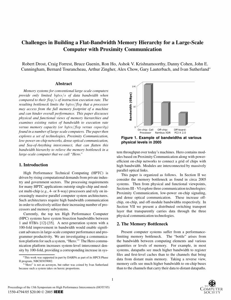
Figure 1. Example of bandwidths at variousphysical levels in 2005
tem throughput over today’s machines. Hero contains mod-ules based on Proximity Communication along with power-efficient on-chip networks to connect a grid of chips withhigh bandwidth. Modules are interconnected by massivelyparallel optical links.
This paper is organized as follows. In Section II weconsider the memory bottleneck as found in circa 2005systems. Then from physical and functional viewpoints,Sections III - VI explore three communication technologies:Proximity Communication, low-power on-chip signaling,and dense optical communication. These increase off-chip, on-chip, and off-module bandwidths respectively. InSection VII we present a distributed switching transportlayer that transparently carries data through the threephysical communication technologies.
2. The Memory Bottleneck
Present computer systems suffer from a performance-limiting memory bottleneck. The “bottle” arises fromthe bandwidth between computing elements and variousquantities or levels of memory. For example, in mostsystems, datapaths see much higher bandwidth to registerfiles and first-level caches than to the channels that bringdata from distant main memory. Taking a reverse view,memory cells see much higher bandwidth to on-chip busesthan to the channels that carry their data to distant datapaths.
1
Proceedings of the 13th Symposium on High Performance Interconnects (HOTI’05)
1550-4794/05 $20.00 © 2005 IEEE
This relationship between bandwidth and memory canbe examined from physical and functional viewpoints. Aphysical classification of the memory hierarchy may containthree principal communication levels: on-chip, off-chip,and off-board. Figure 1 shows high-performance bandwidthexamples: an on-chip Sony-IBM-Toshiba Cell processorinter-core network, an off-chip Rambus XDR memoryinterface, and an off-board PCI-X 2.0 interface [1]-[4]. Thesteep steps, or “cliffs,” from on-chip to off-chip to off-boardbandwidths have historically been a dominating force incomputer architecture.2
The first physical communication level utilizes on-chipwires. Qualitatively, on-chip wires are often characterizedas limiting chip performance. In fact, on-chip wires provideimmense cross-section bandwidth across a VLSI chip [5]and enable multitudes of high performance computing andmemory cells to communicate across a chip.
The second physical communication level is off-chip.Off-chip bandwidth is the product of the number of off-chip channels and the communication rate per channel. Thenumber of off-chip channels in high-performance packagesmay increase at a rate of only about 9% per year overthe next decade [6]. Given this limited increase, workhas been done to increase data rates using, for example,high speed serial transceivers [7],[8]. However thereremains a widening disparity between on-chip cross-sectionbandwidth and off-chip bandwidth.
The third physical communication level is board-to-board. Physical channels may use rigid perpendicularboards connecting through connectors to a backplane, flex-ible channels of twisted-pair or coaxial wires, or fiber op-tic channels in bundled or ribbon configurations. His-torically, electrical connectors provide higher connectioncounts than optical; however, lower attenuation in opticalchannels gives them significant distance and bandwidth ad-vantages over “long” wires. As optical technology costscome down, the definition of “long” has reduced from kilo-meters to meters. Current research has explored using op-tics at the board and even the chip level, although the cost-benefit ratio for optics is presently less compelling than thatfor conventional electrical technologies at those levels.
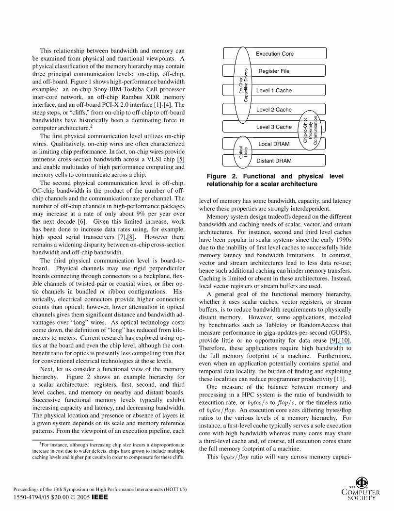
Next, let us consider a functional view of the memoryhierarchy. Figure 2 shows an example hierarchy fora scalar architecture: registers, first, second, and thirdlevel caches, and memory on nearby and distant boards.Successive functional memory levels typically exhibitincreasing capacity and latency, and decreasing bandwidth.The physical location and presence or absence of layers ina given system depends on its scale and memory referencepatterns. From the viewpoint of an execution pipeline, each
2For instance, although increasing chip size incurs a disproportionateincrease in cost due to wafer defects, chips have grown to include multiplecaching levels and higher pin counts in order to compensate for these cliffs.
Execution Core
Register File
Level 1 Cache
Level 2 Cache
Level 3 Cache
Local DRAM
Distant DRAM
On
-Ch
ip:
Ca
pa
citiv
e D
rive
rs
Ch
ip-t
o-C
hip
:
Pro
xim
ity
Co
mm
un
ica
tio
n
Op
tica
l
Lin
ks
Figure 2. Functional and physical levelrelationship for a scalar architecture
level of memory has some bandwidth, capacity, and latencywhere these properties are strongly interdependent.
Memory system design tradeoffs depend on the differentbandwidth and caching needs of scalar, vector, and streamarchitectures. For instance, second and third level cacheshave been popular in scalar systems since the early 1990sdue to the inability of first level caches to successfully hidememory latency and bandwidth limitations. In contrast,vector and stream architectures lead to less data re-use;hence such additional caching can hinder memory transfers.Caching is limited or absent in these architectures. Instead,local vector registers or stream buffers are used.
A general goal of the functional memory hierarchy,whether it uses scalar caches, vector registers, or streambuffers, is to reduce bandwidth requirements to physicallydistant memory. However, some applications, modeledby benchmarks such as Tabletoy or RandomAccess thatmeasure performance in giga-updates-per-second (GUPS),provide little or no opportunity for data reuse [9],[10].Therefore, these applications require high bandwidth tothe full memory footprint of a machine. Furthermore,even when an application potentially contains spatial andtemporal data locality, the burden of finding and exploitingthese localities can reduce programmer productivity [11].
One measure of the balance between memory andprocessing in a HPC system is the ratio of bandwidth toexecution rate, or bytes/s to flop/s , or the timeless ratioof bytes/flop. An execution core sees differing bytes/flopratios to the various levels of a memory hierarchy. Forinstance, a first-level cache typically serves a sole executioncore with high bandwidth whereas many cores may sharea third-level cache and, of course, all execution cores sharethe full memory footprint of a machine.
This bytes/flop ratio will vary across memory capaci-
Proceedings of the 13th Symposium on High Performance Interconnects (HOTI’05)
1550-4794/05 $20.00 © 2005 IEEE
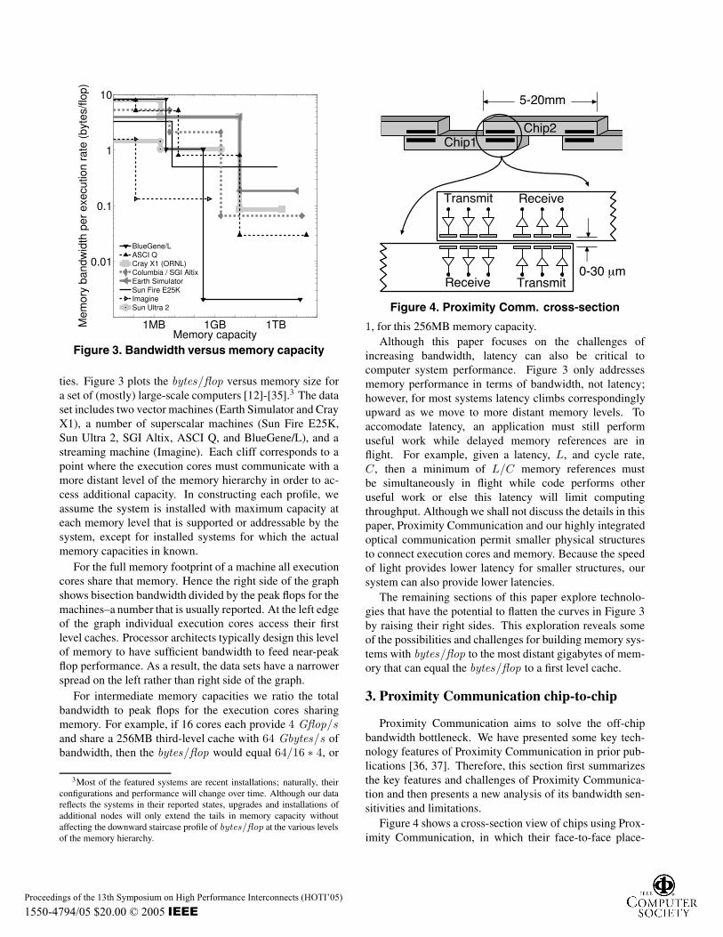
Figure 3. Bandwidth versus memory capacity
ties. Figure 3 plots the bytes/flop versus memory size fora set of (mostly) large-scale computers [12]-[35].3 The dataset includes two vector machines (Earth Simulator and CrayX1), a number of superscalar machines (Sun Fire E25K,Sun Ultra 2, SGI Altix, ASCI Q, and BlueGene/L), and astreaming machine (Imagine). Each cliff corresponds to apoint where the execution cores must communicate with amore distant level of the memory hierarchy in order to ac-cess additional capacity. In constructing each profile, weassume the system is installed with maximum capacity ateach memory level that is supported or addressable by thesystem, except for installed systems for which the actualmemory capacities in known.
For the full memory footprint of a machine all executioncores share that memory. Hence the right side of the graphshows bisection bandwidth divided by the peak flops for themachines–a number that is usually reported. At the left edgeof the graph individual execution cores access their firstlevel caches. Processor architects typically design this levelof memory to have sufficient bandwidth to feed near-peakflop performance. As a result, the data sets have a narrowerspread on the left rather than right side of the graph.
For intermediate memory capacities we ratio the totalbandwidth to peak flops for the execution cores sharingmemory. For example, if 16 cores each provide 4 Gflop/sand share a 256MB third-level cache with 64 Gbytes/s ofbandwidth, then the bytes/flop would equal 64/16 ∗ 4, or
3Most of the featured systems are recent installations; naturally, theirconfigurations and performance will change over time. Although our datareflects the systems in their reported states, upgrades and installations ofadditional nodes will only extend the tails in memory capacity withoutaffecting the downward staircase profile of bytes/flop at the various levelsof the memory hierarchy.
Figure 4. Proximity Comm. cross-section
1, for this 256MB memory capacity.Although this paper focuses on the challenges of
increasing bandwidth, latency can also be critical tocomputer system performance. Figure 3 only addressesmemory performance in terms of bandwidth, not latency;however, for most systems latency climbs correspondinglyupward as we move to more distant memory levels. Toaccomodate latency, an application must still performuseful work while delayed memory references are inflight. For example, given a latency, L, and cycle rate,C, then a minimum of L/C memory references mustbe simultaneously in flight while code performs otheruseful work or else this latency will limit computingthroughput. Although we shall not discuss the details in thispaper, Proximity Communication and our highly integratedoptical communication permit smaller physical structuresto connect execution cores and memory. Because the speedof light provides lower latency for smaller structures, oursystem can also provide lower latencies.
The remaining sections of this paper explore technolo-gies that have the potential to flatten the curves in Figure 3by raising their right sides. This exploration reveals someof the possibilities and challenges for building memory sys-tems with bytes/flop to the most distant gigabytes of mem-ory that can equal the bytes/flop to a first level cache.
3. Proximity Communication chip-to-chip
Proximity Communication aims to solve the off-chipbandwidth bottleneck. We have presented some key tech-nology features of Proximity Communication in prior pub-lications [36, 37]. Therefore, this section first summarizesthe key features and challenges of Proximity Communica-tion and then presents a new analysis of its bandwidth sen-sitivities and limitations.
Figure 4 shows a cross-section view of chips using Prox-imity Communication, in which their face-to-face place-
Proceedings of the 13th Symposium on High Performance Interconnects (HOTI’05)
1550-4794/05 $20.00 © 2005 IEEE
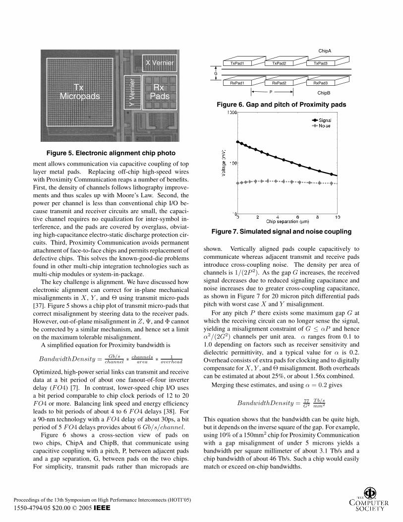
Figure 5. Electronic alignment chip photo
ment allows communication via capacitive coupling of toplayer metal pads. Replacing off-chip high-speed wireswith Proximity Communication reaps a number of benefits.First, the density of channels follows lithography improve-ments and thus scales up with Moore’s Law. Second, thepower per channel is less than conventional chip I/O be-cause transmit and receiver circuits are small, the capaci-tive channel requires no equalization for inter-symbol in-terference, and the pads are covered by overglass, obviat-ing high-capacitance electro-static discharge protection cir-cuits. Third, Proximity Communication avoids permanentattachment of face-to-face chips and permits replacement ofdefective chips. This solves the known-good-die problemsfound in other multi-chip integration technologies such asmulti-chip modules or system-in-package.
The key challenge is alignment. We have discussed howelectronic alignment can correct for in-plane mechanicalmisalignments in X , Y , and Θ using transmit micro-pads[37]. Figure 5 shows a chip plot of transmit micro-pads thatcorrect misalignment by steering data to the receiver pads.However, out-of-plane misalignment in Z , Ψ, and Φ cannotbe corrected by a similar mechanism, and hence set a limiton the maximum tolerable misalignment.
A simplified equation for Proximity bandwidth is
BandwidthDensity = Gb/schannel ∗ channels
area ∗ 1overhead
Optimized, high-power serial links can transmit and receivedata at a bit period of about one fanout-of-four inverterdelay (FO4) [7]. In contrast, lower-speed chip I/O usesa bit period comparable to chip clock periods of 12 to 20FO4 or more. Balancing link speed and energy efficiencyleads to bit periods of about 4 to 6 FO4 delays [38]. Fora 90-nm technology with a FO4 delay of about 30ps, a bitperiod of 5 FO4 delays provides about 6 Gb/s/channel.
Figure 6 shows a cross-section view of pads ontwo chips, ChipA and ChipB, that communicate usingcapacitive coupling with a pitch, P, between adjacent padsand a gap separation, G, between pads on the two chips.For simplicity, transmit pads rather than micropads are
TxPad1 TxPad2 TxPad3
RxPad1 RxPad2 RxPad3
G
P
ChipA
ChipB
Figure 6. Gap and pitch of Proximity pads
Figure 7. Simulated signal and noise coupling
shown. Vertically aligned pads couple capacitively tocommunicate whereas adjacent transmit and receive padsintroduce cross-coupling noise. The density per area ofchannels is 1/(2P 2). As the gap G increases, the receivedsignal decreases due to reduced signaling capacitance andnoise increases due to greater cross-coupling capacitance,as shown in Figure 7 for 20 micron pitch differential padspitch with worst case X and Y misalignment.
For any pitch P there exists some maximum gap G atwhich the receiving circuit can no longer sense the signal,yielding a misalignment constraint of G ≤ αP and henceα2/(2G2) channels per unit area. α ranges from 0.1 to1.0 depending on factors such as receiver sensitivity anddielectric permittivity, and a typical value for α is 0.2.Overhead consists of extra pads for clocking and to digitallycompensate for X , Y , and Θ misalignment. Both overheadscan be estimated at about 25%, or about 1.56x combined.
Merging these estimates, and using α = 0.2 gives
BandwidthDensity = 77G2
Tb/smm2
This equation shows that the bandwidth can be quite high,but it depends on the inverse square of the gap. For example,using 10% of a 150mm2 chip for Proximity Communicationwith a gap misalignment of under 5 microns yields abandwidth per square millimeter of about 3.1 Tb/s and achip bandwidth of about 46 Tb/s. Such a chip would easilymatch or exceed on-chip bandwidths.
Proceedings of the 13th Symposium on High Performance Interconnects (HOTI’05)
1550-4794/05 $20.00 © 2005 IEEE
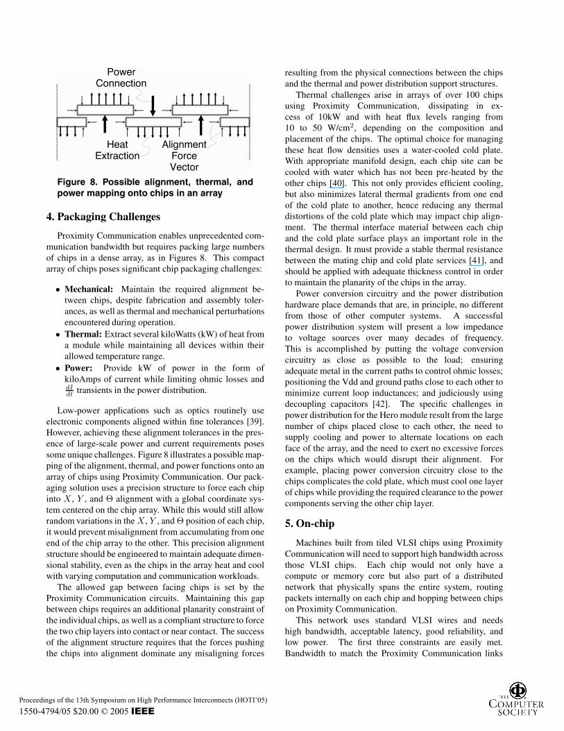
Figure 8. Possible alignment, thermal, andpower mapping onto chips in an array
4. Packaging Challenges
Proximity Communication enables unprecedented com-munication bandwidth but requires packing large numbersof chips in a dense array, as in Figures 8. This compactarray of chips poses significant chip packaging challenges:
• Mechanical: Maintain the required alignment be-tween chips, despite fabrication and assembly toler-ances, as well as thermal and mechanical perturbationsencountered during operation.
• Thermal: Extract several kiloWatts (kW) of heat froma module while maintaining all devices within theirallowed temperature range.
• Power: Provide kW of power in the form ofkiloAmps of current while limiting ohmic losses anddIdt transients in the power distribution.
Low-power applications such as optics routinely useelectronic components aligned within fine tolerances [39].However, achieving these alignment tolerances in the pres-ence of large-scale power and current requirements posessome unique challenges. Figure 8 illustrates a possible map-ping of the alignment, thermal, and power functions onto anarray of chips using Proximity Communication. Our pack-aging solution uses a precision structure to force each chipinto X , Y , and Θ alignment with a global coordinate sys-tem centered on the chip array. While this would still allowrandom variations in the X , Y , and Θ position of each chip,it would prevent misalignment from accumulating from oneend of the chip array to the other. This precision alignmentstructure should be engineered to maintain adequate dimen-sional stability, even as the chips in the array heat and coolwith varying computation and communication workloads.
The allowed gap between facing chips is set by theProximity Communication circuits. Maintaining this gapbetween chips requires an additional planarity constraint ofthe individual chips, as well as a compliant structure to forcethe two chip layers into contact or near contact. The successof the alignment structure requires that the forces pushingthe chips into alignment dominate any misaligning forces
resulting from the physical connections between the chipsand the thermal and power distribution support structures.
Thermal challenges arise in arrays of over 100 chipsusing Proximity Communication, dissipating in ex-cess of 10kW and with heat flux levels ranging from10 to 50 W/cm2, depending on the composition andplacement of the chips. The optimal choice for managingthese heat flow densities uses a water-cooled cold plate.With appropriate manifold design, each chip site can becooled with water which has not been pre-heated by theother chips [40]. This not only provides efficient cooling,but also minimizes lateral thermal gradients from one endof the cold plate to another, hence reducing any thermaldistortions of the cold plate which may impact chip align-ment. The thermal interface material between each chipand the cold plate surface plays an important role in thethermal design. It must provide a stable thermal resistancebetween the mating chip and cold plate services [41], andshould be applied with adequate thickness control in orderto maintain the planarity of the chips in the array.
Power conversion circuitry and the power distributionhardware place demands that are, in principle, no differentfrom those of other computer systems. A successfulpower distribution system will present a low impedanceto voltage sources over many decades of frequency.This is accomplished by putting the voltage conversioncircuitry as close as possible to the load; ensuringadequate metal in the current paths to control ohmic losses;positioning the Vdd and ground paths close to each other tominimize current loop inductances; and judiciously usingdecoupling capacitors [42]. The specific challenges inpower distribution for the Hero module result from the largenumber of chips placed close to each other, the need tosupply cooling and power to alternate locations on eachface of the array, and the need to exert no excessive forceson the chips which would disrupt their alignment. Forexample, placing power conversion circuitry close to thechips complicates the cold plate, which must cool one layerof chips while providing the required clearance to the powercomponents serving the other chip layer.
5. On-chip
Machines built from tiled VLSI chips using ProximityCommunication will need to support high bandwidth acrossthose VLSI chips. Each chip would not only have acompute or memory core but also part of a distributednetwork that physically spans the entire system, routingpackets internally on each chip and hopping between chipson Proximity Communication.
This network uses standard VLSI wires and needshigh bandwidth, acceptable latency, good reliability, andlow power. The first three constraints are easily met.Bandwidth to match the Proximity Communication links
Proceedings of the 13th Symposium on High Performance Interconnects (HOTI’05)
1550-4794/05 $20.00 © 2005 IEEE
between chips comes from the high density of on-chipwires. Wire latency, hampered by the resistive nature ofon-chip wires, can be minimized through wire engineeringand repeater insertion. Reliability arises from circuitssuch as differential signaling, low-offset receivers, andasynchronous handshaking [43][44].
However, the low power constraint is more difficult. AVLSI wire has a total capacitance well approximated byfour parallel plate capacitors plus a fringe term [46],[45];for typical wires, side-to-side capacitance dominates thetotal loading. Wire cap can be approximated at 0.3pFper mm of length ignoring switching effects, and thisvalue changes little under technology scaling. A wirespanning a 15mm die, then, has a total capacitance of 4.5pF,and 256 64-bit buses criss-crossing the chip as part of adistributed system network represent a load of 75nF. Thepower required to swing this capacitance through the powersupply is P ∝ CtotalV
2ddf . At a clock frequency of 4GHz, a
power supply of 1V, and an activity factor of perhaps 0.1, weend up consuming nearly 30W just in network activity. Addin the extra capacitance of repeaters and our wires approachnearly 50W of dissipated power. Clearly, we need someform of power reduction for our on-chip wires.
Many schemes of efficient VLSI wiring have been built[47][48]. They dramatically lower power by reducingsignal swing. By not reducing the power supply as well,these schemes return a linear power savings but avoid thecomplexity of generating and distributing multiple powersupplies to a high-performance VLSI chip. They alsoemploy amplifiers at the receivers to magnify small swingsback to full CMOS voltage levels.
However, low-swing circuits have a couple of importantlimitations. First, pushing a reduced signal swing steponto a long wire still needs a large driver due to thewire’s dominant RC time constant, and these large driversend up consuming most of the power in a low voltage-swing system. Second, the on-chip wires are diffusive,so successive symbols blend and interfere with each other,reducing the fidelity of data transmission and ultimatelylimiting performance. Channel pre-equalization techniquescommon to board-level signaling are too expensive for themultitude of on-chip drivers.
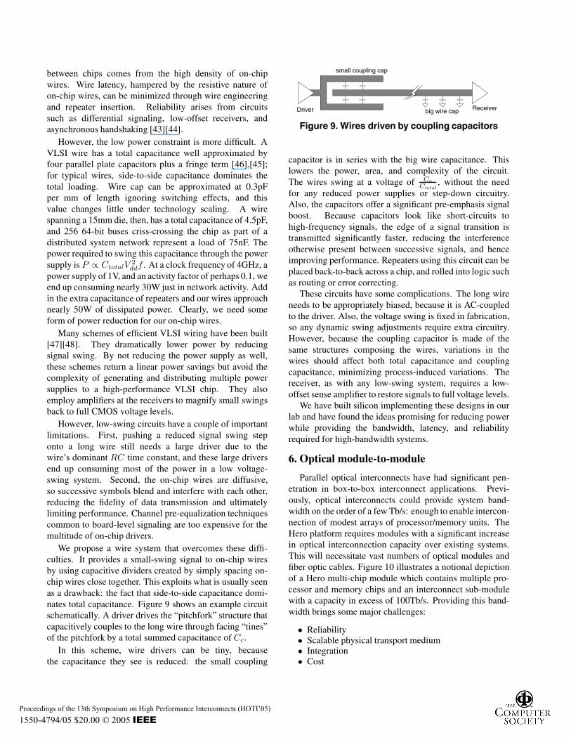
We propose a wire system that overcomes these diffi-culties. It provides a small-swing signal to on-chip wiresby using capacitive dividers created by simply spacing on-chip wires close together. This exploits what is usually seenas a drawback: the fact that side-to-side capacitance domi-nates total capacitance. Figure 9 shows an example circuitschematically. A driver drives the “pitchfork” structure thatcapacitively couples to the long wire through facing “tines”of the pitchfork by a total summed capacitance of Cc.
In this scheme, wire drivers can be tiny, becausethe capacitance they see is reduced: the small coupling
Driver Receiverbig wire cap
small coupling cap
Figure 9. Wires driven by coupling capacitors
capacitor is in series with the big wire capacitance. Thislowers the power, area, and complexity of the circuit.The wires swing at a voltage of Cc
Ctotal, without the need
for any reduced power supplies or step-down circuitry.Also, the capacitors offer a significant pre-emphasis signalboost. Because capacitors look like short-circuits tohigh-frequency signals, the edge of a signal transition istransmitted significantly faster, reducing the interferenceotherwise present between successive signals, and henceimproving performance. Repeaters using this circuit can beplaced back-to-back across a chip, and rolled into logic suchas routing or error correcting.
These circuits have some complications. The long wireneeds to be appropriately biased, because it is AC-coupledto the driver. Also, the voltage swing is fixed in fabrication,so any dynamic swing adjustments require extra circuitry.However, because the coupling capacitor is made of thesame structures composing the wires, variations in thewires should affect both total capacitance and couplingcapacitance, minimizing process-induced variations. Thereceiver, as with any low-swing system, requires a low-offset sense amplifier to restore signals to full voltage levels.
We have built silicon implementing these designs in ourlab and have found the ideas promising for reducing powerwhile providing the bandwidth, latency, and reliabilityrequired for high-bandwidth systems.
6. Optical module-to-module
Parallel optical interconnects have had significant pen-etration in box-to-box interconnect applications. Previ-ously, optical interconnects could provide system band-width on the order of a few Tb/s: enough to enable intercon-nection of modest arrays of processor/memory units. TheHero platform requires modules with a significant increasein optical interconnection capacity over existing systems.This will necessitate vast numbers of optical modules andfiber optic cables. Figure 10 illustrates a notional depictionof a Hero multi-chip module which contains multiple pro-cessor and memory chips and an interconnect sub-modulewith a capacity in excess of 100Tb/s. Providing this band-width brings some major challenges:
• Reliability• Scalable physical transport medium• Integration• Cost
Proceedings of the 13th Symposium on High Performance Interconnects (HOTI’05)
1550-4794/05 $20.00 © 2005 IEEE
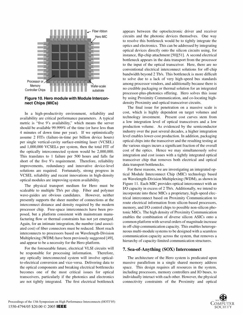
Figure 10. Hero module with Module Intercon-nect Chips (MICs)
In a high-productivity environment, reliability andavailability are critical performance parameters. A typicalmetric is “five 9’s availability,” which means the servershould be available 99.999% of the time (or have less than4 minutes of down time per year). If we optimisticallyassume 2 FITs (failure-in-time per billion device hours)per single vertical-cavity surface-emitting laser (VCSEL)and 1,000,000 VCSELs per system, then the total FIT ofthe optically interconnected system would be 2,000,000.This translates to 1 failure per 500 hours and falls farshort of the five 9’s requirement. Therefore, reliabilityimprovements, redundancy and innovative device-levelsolutions are required. Fortunately, strong progress inVCSEL reliability and recent innovations in high-densityoptical modules are improving system availability.
The physical transport medium for Hero must bescaleable to multiple Tb/s per chip. Fiber and polymerwave-guides are obvious candidates. However, neitherpresently supports the sheer number of connections at theinterconnect distance and density required by the modernprocessor chip. Free-space interconnects have been pro-posed, but a platform consistent with mainstream manu-facturing flow or thermal constraints has not yet emerged.Again, for an intimate integration, the number (and associ-ated cost) of fiber connectors must be reduced. Short reachinterconnects to processors based on Wavelength-DivisionMultiplexing (WDM) have been previously suggested [49],and appear to be a necessity for the Hero platform.
For the foreseeable future, electrical VLSI circuits willbe responsible for processing information. Therefore,any optically interconnected system will involve optical-to-electrical conversion and vice-versa. Delivering data tothe optical components and breaking electrical bottlenecksbecomes one of the most critical issues for opticaltransceivers, particularly if the photonics and electronicsare not tightly integrated. The first electrical bottleneck
appears between the optoelectronic driver and receivercircuits and the photonic devices themselves. One wayto resolve this bottleneck would be to tightly integrate theoptics and electronics. This can be addressed by integratingoptical devices directly onto the silicon circuits using, forinstance, flip-chip attachment [50][51]. A second electricalbottleneck appears in the data transport from the processorto the input of the optical transceiver. Here, there are noconventional electrical interconnect solutions for off-chipbandwidth beyond 2 Tb/s. This bottleneck is more difficultto solve due to a lack of very high-speed bus standardsamong processor vendors, and additionally because there isno credible packaging or thermal solution for an integratedprocessor-plus-photonics offering. Hero solves this issueby using Proximity Communication, and co-locating high-density Proximity and optical transceiver circuits.
The final issue for penetration on a massive scale iscost, which is highly dependent on target volumes andtechnology investment. Present cost curves stem froma low integration level of optical transceivers and a lowproduction volume. As evidenced by the semiconductorindustry over the past several decades, a higher integrationlevel enables lower-cost production. In addition, packagingoptical chips into the transceiver and the resulting testing atthe various stages incurs a significant fraction of the overallcost of the optics. Hence we may simultaneously solveintegration and cost issues with a tightly integrated opticaltransceiver chip that removes both electrical and opticaldata transport bottlenecks.
For these reasons, we are investigating an integrated op-tical Module Interconnect Chip (MIC) technology basedon Wavelength-Division Multiplexing (WDM), as shown inFigure 11. Each MIC provides optical interconnect with anI/O capacity in excess of 2 Tb/s. Additionally, we intend toincorporate into these MICs a proprietary, high-speed elec-trical interconnect based on Proximity Communication toroute electrical information from silicon-based processors,memory, and I/O control chips to possible non-silicon pho-tonic MICs. The high density of Proximity Communicationenables the combination of diverse silicon ASICs onto acommon platform with several orders of magnitude increasein off-chip communication capacity. This enables heteroge-neous multi-module systems to be designed with a seamlesscommunication capacity across the system, that removes ahierarchy of capacity-limited communication structures.
7. Sea-of-Anything (SOX) Interconnect
The architecture of the Hero system is predicated uponmassive parallelism in a single shared memory addressspace. This design requires all resources in the system,including processors, memory controllers and IO buses, toindividually interact with each other. However, the physicalconnectivity constraints of the Proximity and optical
Proceedings of the 13th Symposium on High Performance Interconnects (HOTI’05)
1550-4794/05 $20.00 © 2005 IEEE
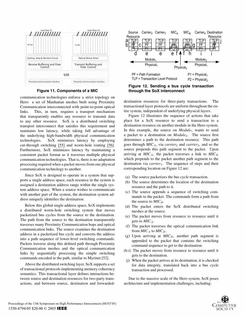
Figure 11. Components of a MIC
communication technologies enforce a strict topology onHero: a set of Manhattan meshes built using ProximityCommunication interconnected with point-to-point opticallinks. This, in turn, requires a transport mechanismthat transparently enables any resource to transmit datato any other resource. SoX is a distributed switchingtransport interconnect that satisfies this requirement andmaintains low latency, while taking full advantage ofthe underlying high-bandwidth physical communicationtechnologies. SoX minimizes latency by employingcut-through switching [55] and worm-hole routing [56].Furthermore, SoX minimizes latency by maintaining aconsistent packet format as it traverses multiple physicalcommunication technologies. That is, there is no adaptationprocessing required when a packet moves from one physicalcommunication technology to another.
Since SoX is designed to operate in a system that sup-ports a single address space, each resource in the system isassigned a destination address range within the single sys-tem address space. When a source wishes to communicatewith another part of the system, the destination system ad-dress uniquely identifies the destination.
Below this global single address space, SoX implementsa distributed worm-hole switching system that movespacketized bus cycles from the source to the destination.The path from the source to the destination transparentlytraverses many Proximity Communication hops and opticalcommunication links. The source examines the destinationaddress in a packetized bus cycle and converts the addressinto a path sequence of lower-level switching commands.Packets traverse along this defined path through ProximityCommunication meshes and the optical communicationlinks by sequentially processing the simple switchingcommands encoded in the path, similar to Myrinet [52].
Above the distributed switching layer, SoX supports a setof transactional protocols implementing memory coherencysemantics. This transactional layer defines interactions be-tween source and destination resources for two-party trans-actions, and between source, destination and forwarded-
Figure 12. Sending a bus cycle transactionthrough the SoX interconnect
destination resources for three-party transactions. Thetransactional layer protocols are uniform throughout the en-tire system, independent of underlying physical layers.
Figure 12 illustrates the sequence of actions that takeplace for a SoX resource to send a transaction to adestination resource on another module in the Hero system.In this example, the source on Module1 wants to senda packet to a destination on Module2. The source firstdetermines a path to the destination resource. This pathgoes through MICA, via carrier2 and carrier3, and so thesource prepends this path segment to the packet. Uponarriving at MICA, the packet traverses a link to MICB
which prepends to the packet another path segment to thedestination via carrier4. The sequence of steps and theircorresponding location on Figure 12 are:
(a) The source packetizes the bus cycle transaction.(b) The source determines the location of the destination
resource and the path to it.(c) The source appends a sequence of switching com-
mands to the packet. The commands form a path fromthe source to MICB .
(d) The packet enters the SoX distributed switchingmeshes at the source.
(e) The packet moves from resource to resource until itgets to MICA.
(f) The packet traverses the optical communication linkfrom MICA to MICB .
(g) Upon arriving at MICB , another path segment isappended to the packet that contains the switchingcommand sequence to get to the destination.
(h-i) The packet moves from resource to resource until itgets to the destination.
(j) When the packet arrives at its destination, it is checkedfor data integrity, translated back into a bus cycletransaction and processed.
Due to the massive scale of the Hero system, SoX posesarchitecture and implementation challenges, including:
Proceedings of the 13th Symposium on High Performance Interconnects (HOTI’05)
1550-4794/05 $20.00 © 2005 IEEE
• Avoiding deadlocks in distributed switching meshes
• Achieving fault tolerance as parts of the distributedswitching fabric fail
• Maintaining and updating the path tables that re-sources use to form switching command sequenceswhen creating a packetized bus cycle
The combination of worm-hole routing and Manhattanswitching meshes creates the challenge of avoiding dead-locks in the switching meshes. Packet switching deadlockoccurs when packets block each other in a cyclical man-ner. SoX avoids the problem of packet switching deadlockby guaranteeing that the union of all possible packet pathsconforms to a Directed Acyclic Graph [57], regardless ofhow malformed packets may become, thus eliminating thepossibility for cyclic dependencies [58, 59].
Addressing the fault-tolerance challenge requires detect-ing faults which may be caused by failures of resources orparts of the communication fabric, and taking immediatecorrective actions. These actions may vary from a simpleretransmission to reassigning communication and comput-ing tasks to alternate resources. One of the techniques em-ployed to detect faults is to require all SoX transactions tobe positively acknowledged. So when a source does not re-ceive a positive acknowledgement within a certain timeoutperiod, a potential fault has been detected. This timeoutevent triggers an immediate retransmission of the transac-tion on an independent, disjoint path. Continued timeoutsinitiate an out-of-band system to locate the source of theproblem and prepare a new set of paths to isolate and cir-cumvent the faulty resources or communication links.
Addressing the path table challenge requires the abilityfor all path tables in a SoX interconnect to be recomputedand updated upon any change of a system’s topology. Someof the events that trigger this activity include, but are notlimited to, system power-up, isolation of faulty componentsor the re-integration of repaired components. When mostresources are operational in a system, the computation ofpath tables is relatively simple. However, when a systemhas many components that have been isolated due to failure,the updating of these path tables becomes much morecomplicated. Research into algorithms that can cope withthe scale of a Hero class system and handle large numbersof random failures is ongoing.
8. Summary
This paper examines the memory bottleneck in large-scale computers, exploring it from both physical andfunctional viewpoints and considering system balanceusing the ratio of bytes/flop versus memory capacity.Additionally, it proposes a computer we term “Hero,” thataims to achieve a much flatter memory hierarchy.
The paper presents the key features and challenges ofthree high-bandwidth physical technologies that can be usedin Hero: Proximity Communication, low-power on-chipnetworks, and dense optical communication. ProximityCommunication provides orders of magnitude improvementin off-chip bandwidth compared to traditional I/O, but haskey alignment challenges. We develop a simple analyticmodel for the trade-off between alignment accuracy andachievable bandwidth. Our on-chip networks provideample bandwidth and address power concerns with a newcapacitively-coupled driver circuit. Optical communicationuses dense WDM combined with Proximity circuits toaddress important optical challenges.
In addition, the paper discusses a transport layer, SoX,that is a provably deadlock-free high-bandwidth low-latency two-level interconnect fabric. SoX uses ProximityCommunication meshes for inter-chip communication andWDM fiber optics for inter-module communication. SoXalso includes means to detect and to handle deadlocks thatarise from equipment malfunction.
Together these technologies have the potential to flattenthe bandwidth hierarchy of large-scale computers to main-tain high bytes/flop across all levels of caching, out to thefull memory footprint of a machine. Presently, most code isplanned and generated with the expected constraint of mem-ory hierarchies that provide ever-decreasing bandwidths tolarger sets of memory. With the technologies describedhere, hardware and software architects can look towards de-signing systems, compilers, and applications that effectivelyutilize a much flatter bandwidth hierarchy.
9. Acknowledgments
We acknowledge every member of Sun’s HPCS team,led by Jim Mitchell and supported by Greg Papadopoulos.In addition we recognize the effective support and guidancefrom DARPA as part of its HPCS Phase II program.
References
[1] D. Pham, et al., “The Design and Implementation of a First-Generation CELL Processor,” IEEE ISSCC, Feb 2005.
[2] W. Beyene et al., “Design and analysis methodologies of a6.4 Gb/s memory interconnect system,” Electronic Comp.and Tech., pp. 1406-1411, June 2004.
[3] “XDR XIO Data Sheet Summary,” www.rambus.com.[4] “PCI-X 2.0: High Performance, Backward Compatible PCI
for the Future,” www.pcisig.com.[5] R. Ho, K. Mai, and M. Horowitz, “The Future of Wires,”
Proceedings of the IEEE, pp. 490-504, April 2001.[6] Int’l Technology Roadmap for Semiconductors, 2003.[7] C.-K. K. Yang et al., “A 0.5um CMOS 4Gb/s serial link
transceiver with data recovery using oversampling,” IEEEJournal of Solid-State Circuits, pp. 713-722, May 1998.
[8] R. Drost and B. Wooley, “An 8-Gb/s/pin SimultaneouslyBidirectional Transceiver in 0.35-micron CMOS,” IEEEJournal of Solid-State Circuits, pp. 1894-1908, Nov. 2004.
Proceedings of the 13th Symposium on High Performance Interconnects (HOTI’05)
1550-4794/05 $20.00 © 2005 IEEE

[9] J. Gustafson, “Purpose-Based Benchmarks” Int’l J of HighPerf. Computing Applications, Vol. 18, pp. 475-487, 2004.
[10] J. McCalpin, “Memory Bandwidth and Machine Balancein Current High Performance Computers,” IEEE TechnicalCommittee on Comp. Arch. (TCCA) Newsletter, Dec 1995.
[11] T. Chilimbi et al., “Making Pointer-Based Data StructuresCache Conscious,” IEEE Computer, pp. 67-74, Dec 2000.
[12] H. Meuer et al., Universities of Mannheim and Tennessee,Top500 Supercomputer Sites, www.top500.org.
[13] N. Adiga et al., “An overview of the BlueGene/L supercom-puter,” Proc. ACM/IEEE Conf. Supercomputing, 2002.
[14] F. Allen et al., “Blue Gene,” IBM System Journal, Vol. 40,No. 2, 2001, pp. 310-327.
[15] D. J. Kerbyson et al., “A comparison between the EarthSimiulator and AlphaServer systems using predictive appli-cation performance models,” Proc. Intl. Parallel and Dis-tributed Processing Symp., April 2003.
[16] SGI Altix 3000 Hardware, www.nas.nasa.gov/Users/ Docu-mentation/ Altix/hardware.html.
[17] T. Dunigan et al., “Early Evaluation of the Cray X1,” inProc. ACM/IEEE Conf. Supercomputing, 2003.
[18] H. Shan and E. Strohmaier, “Performance characteristicsof the Cray X1 and their implications for application perf.tuning,” Supercomputing Conf., pp. 175-83, 2004.
[19] K. Krewell, “UltraSPARC IV mirrors predecessor,” Micro-processor Report, November 2003, pp. 1-3.
[20] Sun Fire E25K Datasheet, www.sun.com/ servers/highend.[21] A. J. van der Steen and J. Dongarra, “Overview of recent
supercomputers,” www.top500.org/ORSC/2004.[22] Ultra2 Workstation Architecture, Sun Microsystems, 1999.[23] T. Sato, et al., “Earth Simulator Running,” Intl. Supercom-
puting Conf., Heidelberg, June 2002.[24] S. Habata, et al., “The Earth Simulator system,” NEC
Research and Development, Vol. 44, January 2003.[25] UltraSPARC IV Processor Architecture Overview, Sun
Microsystems technical white paper, 2004.[26] S. Naffziger, et al., “The implementation of the Itanium 2
microprocessor,” IEEE Journal of Solid-State Circuits, Vol.37, No. 11, November 2002, pp. 1448-1460.
[27] H. Sharangpani and K. Arora, “Itanium processor microar-chitecture,” IEEE Micro, pp. 24-43, Sept-Oct 2000.
[28] R. E. Kessler, “The Alpha 21264 Microprocessor,” IEEEMicro, Vol. 19, No. 2, March-April 1999, pp. 24-36.
[29] J. Borkenhagen et al., “A multithreaded PowerPC processorfor commercial servers,” IBM Journal of Research andDevelopment, Vol. 44, No. 6, November 2000, pp. 885-898.
[30] A. Klauser, “Trends in high-performance microprocessordesign,” Telematik-2001, No. 1, pp. 12-21, 2001.
[31] R. E. Kessler, et al., “The Alpha 21264 MicroprocessorArchitecture,” IEEE ICCD, pp. 90-5, Oct 1998.
[32] B. Khailany et al., “Imagine: media processing withstreams,” IEEE Micro, Vol. 21, pp. 35-46, Mar-Apr 2001.
[33] U. Kapasi et al., “The Imagine stream processor,” Proc.2002 IEEE Intl. Conf. Computer Design: VLSI in Computersand Processors, pp. 282-288, September 2002.
[34] B. Serebrin et al., “A stream processor developmentplatform,” IEEE ICCD, pp. 303-8, Sept 2002.
[35] L. Oliker et al., “Scientific computations on modernparallel vector systems,” Proc. ACM/IEEE SC2004 Conf.Supercomputing, November 2004, pp. 10.
[36] R. Drost, et al., “Proximity Communication,” IEEE JSSC,pp. 1529-35, Sept. 2004.
[37] R. Drost, et al., “Electronic Alignment for ProximityCommunication,” IEEE ISSCC, Feb. 2004.
[38] M.-J. E. Lee et al., “Low-Power Area-Efficient High-SpeedI/O Circuit Techniques,” IEEE JSSC, Nov. 2000.
[39] W. J. Shakespeare et al., “MEMS Integrated SubmountAlignment for Optoelectronics,” Journal Of LightwaveTechnology, pp. 504-509, 2005.
[40] D. W. Copeland et al., “Manifold Microchannel HeatSinks: Isothermial Analysis,” Proceedings, InterSocietyConference on Thermal Phenomena, pp, 251-257, 1966.
[41] B. Guenin, “Calculations for Thermal Interface Materials,”Electronics Cooling, Vol 9, No. 3, August, 2003.
[42] L.D. Smith, et al., “Power Distribution Sys. Design Meth.and Capacitor Selection for Modern CMOS Tech.,” IEEETransactions on Advanced Packaging, pp. 284-91, 1999.
[43] I. Sutherland, J. Lexau, “Designing Fast AsynchronousCircuits,” IEEE Async 2001, pp. 184-193, March 2001.
[44] R. Ho, J. Gainsley, R. Drost, “Long wires and asynchronouscontrol,” IEEE Async 2004, pp. 240-249, April 2004.
[45] R. Ho, et al., “Managing Wire Scaling: A CircuitPerspective,” IEEE Int’l Interconnect Tech. Conf., Jun 2003.
[46] M. Bohr, “Interconnect Scaling–The Real Limiter To High-Performance ULSI,” IEEE Electron Devices Meeting, pp.241-244, December 1995.
[47] H. Zhang et al., “Low-swing on-chip signaling techniques,”IEEE Transactions on VLSI, pp. 414-419, April 1993.
[48] R. Ho, et al., “Efficient On-Chip Global Interconnects,”IEEE Symposium on VLSI Circuits, June 2003.
[49] A. V. Krishnamoorthy et al., “AMOEBA: an optoelectronicswitch for multiproc. networking using dense-WDM,” IEEEJ. Special Topics in Quantum Elec., pp. 261-75, Mar 1999.
[50] K. W. Goossen and A. V. Krishnamoorthy, “Optoelec-tronics-in-VLSI,” in Wiley Encyclopedia of Electrical andElectronic Engineering Vol. 15, pp. 380-395, 1999.
[51] A. V. Krishnamoorthy et al., “Fibre-to-the-chip: VCSELarrays for integration with VLSI circuits,” in Handbook ofLaser Tech. and Applications: Vol. 3 Ed. C., UK, Dec. 2003.
[52] N. Boden, et al., “Myrinet: A Gigabit-per-second LocalArea Network,” IEEE-Micro, pp. 29-36, Feb 1995.
[53] P. Palnati et al., “Deadlock-free routing in an opticalinterconnect for high-speed wormhole routing networks,”ICPADS, 1996.
[54] J.E. Cunningham, et al., “Scaling VCSEL reliability up to250Terabits/s of system bandwidth,” OSA Topical Meetingon Information Photonics, June 2005.
[55] P. Kermani and L. Kleinrock, “Virtual Cut-through: ANew Computer Communication Switching Technique,”Computer Networks, pp. 267-86, Sep. 1979.
[56] W. J. Dally, and C. L. Seitz, “Deadlock-free messagerouting in multiprocessor interconnection networks,” IEEETransactions Comp., pp. 547-53, May 1987.
[57] F. Harary and E. M. Palmer, Graphical Enumeration,Academic Press, New York, 1973.
[58] C. Glass and L. Ni, “The turn model for adaptive routing,”J. ACM, pp. 874-902, 1994.
[59] E. Fleury et al., “A General Theory for Deadlock Avoidancein Wormhole-Routed Networks,” IEEE Trans. ParallelDistrib. Syst., pp. 626-38, 1998.
[60] J.-S. Yang and C.-T. King, “Designing Deadlock-Free Turn-Restricted Routing Algorithms for Irregular Wormhole-Routed Network”, J. Information Science and Engineering,pp. 575-94, 2001.
Proceedings of the 13th Symposium on High Performance Interconnects (HOTI’05)
1550-4794/05 $20.00 © 2005 IEEE
Related Documents