From Principles of Electronic Materials and Devices, Third Edition, S.O. Kasap (© McGraw-Hill, 2005) Chapter 5 Semiconductors

Welcome message from author
This document is posted to help you gain knowledge. Please leave a comment to let me know what you think about it! Share it to your friends and learn new things together.
Transcript

From Principles of Electronic Materials and Devices, Third Edition, S.O. Kasap (© McGraw-Hill, 2005)
Chapter 5 Semiconductors

Homework
• Problem to be quizzed on Week of Nov. 8 – 5.1, 5.2, 5.3,5.4, 5.6, 5.7, 5.8, 5.9, 5.10, 5.12
5.13. – Worked examples: 5.1, 5.2, 5.3, 5.4, 5.5, 5.6,
5.7, 5.8, 5.9, 5.11.
From Principles of Electronic Materials and Devices, Third Edition, S.O. Kasap (© McGraw-Hill, 2005)

From Principles of Electronic Materials and Devices, Third Edition, S.O. Kasap (© McGraw-Hill, 2005)
Silicon is the most important semiconductor in today’s electronics |SOURCE: Courtesy of IBM

From Principles of Electronic Materials and Devices, Third Edition, S.O. Kasap (© McGraw-Hill, 2005)
200 mm and 300 mm Si wafers. |SOURCE: Courtesy of MEMC, Electronic Materials, Inc.

From Principles of Electronic Materials and Devices, Third Edition, S.O. Kasap (© McGraw-Hill, 2005)
GaAs ingots and wafers. GaAs is used in high speed electronic devices, and optoelectronics. |SOURCE: Courtesy of Sumitomo Electric Industries, Ltd.
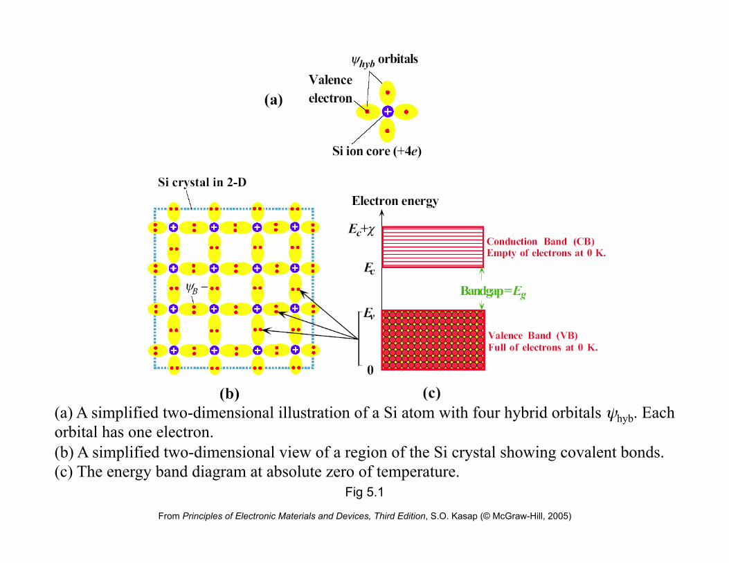
Fig 5.1
From Principles of Electronic Materials and Devices, Third Edition, S.O. Kasap (© McGraw-Hill, 2005)
(a) A simplified two-dimensional illustration of a Si atom with four hybrid orbitals ψhyb. Each orbital has one electron. (b) A simplified two-dimensional view of a region of the Si crystal showing covalent bonds. (c) The energy band diagram at absolute zero of temperature.
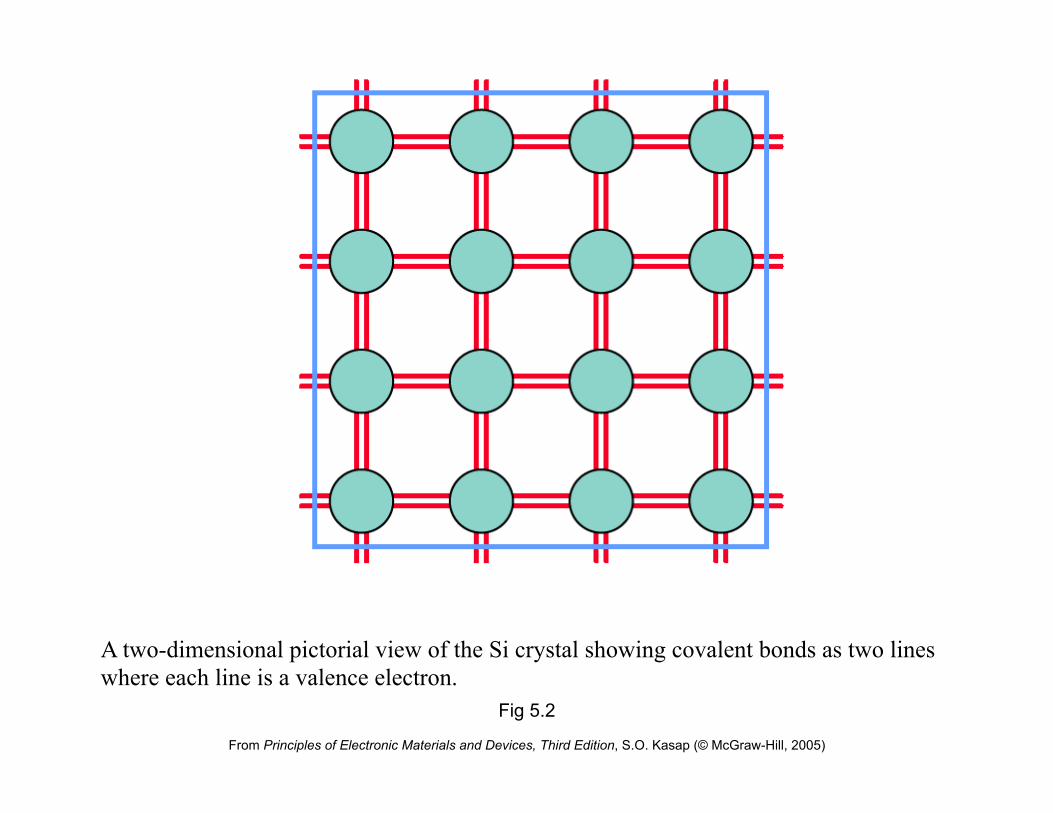
Fig 5.2
From Principles of Electronic Materials and Devices, Third Edition, S.O. Kasap (© McGraw-Hill, 2005)
A two-dimensional pictorial view of the Si crystal showing covalent bonds as two lines where each line is a valence electron.

Fig 5.3
From Principles of Electronic Materials and Devices, Third Edition, S.O. Kasap (© McGraw-Hill, 2005)
(a) A photon with an energy greater than Eg can excite an electron from the VB to the CB.
(b) When a photon breaks a Si-Si bond, a free electron and a hole in the Si-Si bond is created.
Electron-Hole Pair, EHP

Fig 5.4
From Principles of Electronic Materials and Devices, Third Edition, S.O. Kasap (© McGraw-Hill, 2005)
Thermal vibrations of atoms can break bonds and thereby create electron-hole pairs.

Fig 5.5
From Principles of Electronic Materials and Devices, Third Edition, S.O. Kasap (© McGraw-Hill, 2005)
A pictorial illustration of a hole in the valence band wandering around the crystal due to the tunneling of electrons from neighboring bonds.
From Principles of Electronic Materials and Devices, Third Edition, S.O. Kasap (© McGraw-Hill, 2005)
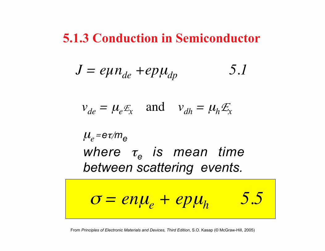
5.1.3 Conduction in Semiconductor
J = eµnde +epµdp 5.1
vde = µeEx and vdh = µhEx
µe= eτ/me where τe is mean time between scattering events.
σ = enµe + epµh 5.5

Fig 5.6
From Principles of Electronic Materials and Devices, Third Edition, S.O. Kasap (© McGraw-Hill, 2005)
When an electric field is applied, electrons in the CB and holes in the VB can drift and contribute to the conductivity. (a) A simplified illustration of drift in Ex. (b) Applied field bends the energy bands since the electrostatic PE of the electron is –eV(x) and V(x) decreases in the direction of Ex, whereas PE increases.

From Principles of Electronic Materials and Devices, Third Edition, S.O. Kasap (© McGraw-Hill, 2005)
Electron and Hole Drift Velocities
vde = drift velocity of the electrons, µe = electron drift mobility, Ex = applied electric field, vdh = drift velocity of the holes, µh = hole drift mobility
vde = µeEx and vdh = µhEx
Conductivity of a Semiconductor
σ = conductivity, e = electronic charge, n = electron concentration in the CB, µe = electron drift mobility, p = hole concentration in the VB, µh = hole drift mobility
σ = enµe + epµh

Fig 5.7
From Principles of Electronic Materials and Devices, Third Edition, S.O. Kasap (© McGraw-Hill, 2005)
(a) Energy band diagram.
(b) Density of states (number of states per unit energy per unit volume).
(c) Fermi-Dirac probability function (probability of occupancy of a state).
(d) The product of g(E) and f (E) is the energy density of electrons in the CB (number of electrons per unit energy
per unit volume). The area under nE(E) versus E is the electron concentration.

From Principles of Electronic Materials and Devices, Third Edition, S.O. Kasap (© McGraw-Hill, 2005)
If you multiply g(E) by f(E) and integrate you get # of electrons per unit energy per unit volume, nE.
!
n =o
Top of band
" nEdE = g(E) f (E)o
Top of band
" dE
!
n =8" 2me
3 / 2
h3E1/2
1+exp(E - EF
kT)o
#
$ dE 4.21
From Ch. 4

If you multiply g(E) by f(E) you get # of electrons per unit energy per unit volume, nE.
!
n =o
Top of band
" nEdE = g(E) f (E)o
Top of band
" dE
!
n = gCB (E) f (E) Ec
Ec +"
# dE
For Semiconductors

Assuming Ec – EF >> kT then Fermi-Dirac degenerates to Boltzmann distribution, or:
From Principles of Electronic Materials and Devices, Third Edition, S.O. Kasap (© McGraw-Hill, 2005)
!
f (E) = exp - (E - EF
kT)
For Semiconductors
!
n = 8" 2( ) me*
h2
#
$ %
&
' (
3 / 2
(E - Ec)1/2exp - (
E - EF
kT)
Ec
)
* dE
!
g(E) = 8" 2( ) me*
h2
#
$ %
&
' (
3 / 2
(E ) Ec )1/ 2
Assume DOS, g(E), is that of free electrons (see next slide), then

Fig 5.7
From Principles of Electronic Materials and Devices, Third Edition, S.O. Kasap (© McGraw-Hill, 2005)
To find integral, One important approx was made: We only worried about shape of g(E) near the band edge. This allows us to use Eq. 4.10 for an electron in a 3-D well.

From Principles of Electronic Materials and Devices, Third Edition, S.O. Kasap (© McGraw-Hill, 2005)
Electron Concentration in CB
n = electron concentration in the CB, Nc = effective density of states at the CB edge, Ec = conduction band edge, EF = Fermi energy, k = Boltzmann constant, T = temperature
Effective Density of States at CB Edge
Nc = effective density of states at the CB edge, me* = effective mass of the electron
in the CB, k = Boltzmann constant, T = temperature, h = Planck’s constant
!
n = Nc exp "(Ec " EF )
kT#
$ % &
' ( 5.6
!
Nc = 2 2"me*kT
h2
#
$ %
&
' (
3 / 2
5.7

From Principles of Electronic Materials and Devices, Third Edition, S.O. Kasap (© McGraw-Hill, 2005)
Hole Concentration in VB
p = hole concentration in the VB, Nv = effective density of states at the VB edge, EF = Fermi energy, Ev = valence band edge, k = Boltzmann constant, T = temperature
Effective Density of States at VB Edge
Nv = effective density of states at the VB edge, mh* = effective mass of a hole in the
VB, k = Boltzmann constant, T = temperature, h = Planck’s constant
!
p = Nv exp "(EF " Ev )
kT#
$ % &
' ( 5.8
!
Nv = 2 2"mh*kT
h2
#
$ %
&
' (
3 / 2
5.9

From Principles of Electronic Materials and Devices, Third Edition, S.O. Kasap (© McGraw-Hill, 2005)
Mass Action Law
If you have thermal equilibrium, then 5.10 is always true for most semiconductors.
For intrinsic semiconductor, n = p and
!
np = ni2 = NcNv exp "
Eg
kT#
$ %
&
' ( 5.11
ni = intrinsic concentration
!
np = NcNv exp "Eg
kT#
$ %
&
' ( 5.10
Only depends on T

Useful Exercise
• Derive Eqs. 5.6 and 5.8. • Derive Eq. 5.10.
From Principles of Electronic Materials and Devices, Third Edition, S.O. Kasap (© McGraw-Hill, 2005)

• For an intrinsic SC, n = p = ni. • So if you equate the 2 equations and take ln
p = Nv exp !(EF !Ev )
kT
"
#$
%
&' 5.8
!
np = ni2 = NcNv exp "
Eg
kT#
$ %
&
' ( 5.11
ni = intrinsic concentration
!
EFi = Ev +12Eg "
12kT ln Nc
Nv
#
$ %
&
' ( 5.12

Fermi Energy in Intrinsic Semiconductors
!
EFi = Ev +12Eg "
12kT ln Nc
Nv
#
$ %
&
' ( 5.12
me* = electron effective mass (CB), mh
* = hole effective mass (VB)
!
EFi = Ev +12Eg "
34kT ln me
*
mh*
#
$ %
&
' ( 5.13
!
Nv = 2 2"mh*kT
h2
#
$ %
&
' (
3 / 2
5.9
!
Nc = 2 2"me*kT
h2
#
$ %
&
' (
3 / 2
5.7
If Nc = Nv or m*e m*h, then
!
EFi = Ev +12Eg

Fig 5.8
From Principles of Electronic Materials and Devices, Third Edition, S.O. Kasap (© McGraw-Hill, 2005)
In all cases, np = ni2
!
EFi = Ev +12Eg "
34kT ln me
*
mh*
#
$ %
&
' ( = Ev +
12Eg
Intrinsic n-type p-type
If me* = mh* then

From Principles of Electronic Materials and Devices, Third Edition, S.O. Kasap (© McGraw-Hill, 2005)
For or an intrinsic SC, Eg falls in the middle of the band gap. For a n-type SC, n > p and Ef is closer to Ec For a p-type SC, p > n and Ef is closer to Ev.

!
E CB =1n
ECB" gcb (E) f (E)dE
Average energy of electrons in CB
!
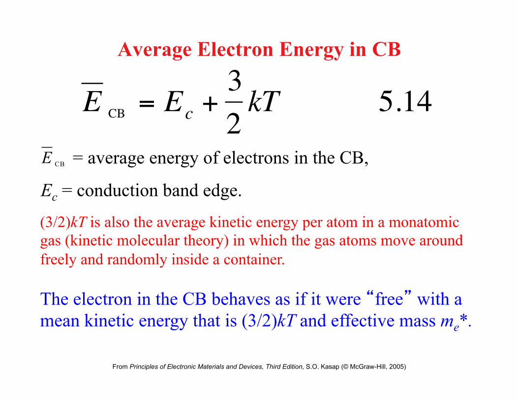
E CB = Ec +32kT 5.14
From Principles of Electronic Materials and Devices, Third Edition, S.O. Kasap (© McGraw-Hill, 2005)
Average Electron Energy in CB
!
E CB = Ec +32kT 5.14
= average energy of electrons in the CB,
Ec = conduction band edge. CBE
(3/2)kT is also the average kinetic energy per atom in a monatomic gas (kinetic molecular theory) in which the gas atoms move around freely and randomly inside a container.
The electron in the CB behaves as if it were “free” with a mean kinetic energy that is (3/2)kT and effective mass me*.

From Principles of Electronic Materials and Devices, Third Edition, S.O. Kasap (© McGraw-Hill, 2005)

From Principles of Electronic Materials and Devices, Third Edition, S.O. Kasap (© McGraw-Hill, 2005)
5.2 Extrinsic Semiconductors
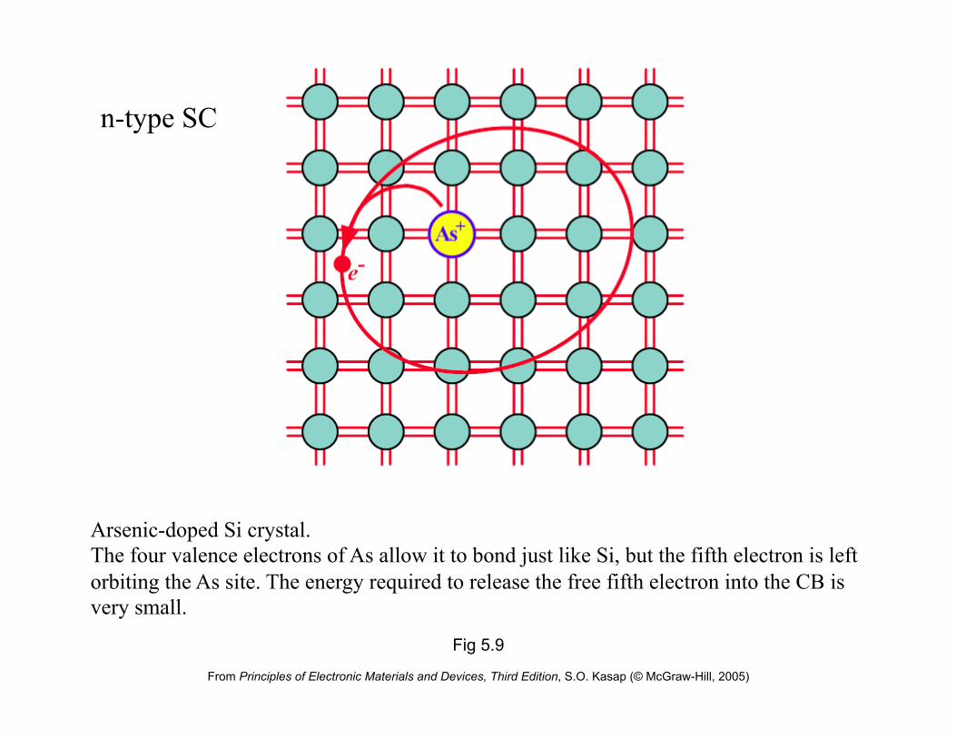
Fig 5.9
From Principles of Electronic Materials and Devices, Third Edition, S.O. Kasap (© McGraw-Hill, 2005)
Arsenic-doped Si crystal. The four valence electrons of As allow it to bond just like Si, but the fifth electron is left orbiting the As site. The energy required to release the free fifth electron into the CB is very small.
n-type SC

Fig 5.10
From Principles of Electronic Materials and Devices, Third Edition, S.O. Kasap (© McGraw-Hill, 2005)
Energy band diagram for an n-type Si doped with 1 ppm As. There are donor energy levels just below Ec around As+ sites.

N-type Conductivity
e = electronic charge Nd = donor atom concentration in the crystal
µe = electron drift mobility, ni = intrinsic concentration, µh = hole drift mobility
!
" = eNdµe +e ni2
Nd
#
$ % %
&
' ( ( µh ) eNdµe 5.16
!
" = eNdµe 5.16

From Principles of Electronic Materials and Devices, Third Edition, S.O. Kasap (© McGraw-Hill, 2005)
Occupation Probability at a Donor
fd(Ed ) = probability of finding an electron in a state with energy Ed at a donor
Ed = energy level of donor
½ comes from the fact that donor
can only take one electron
!
fd (Ed ) =1
1+12
exp (Ed "EF )kT
#
$ % &
' (
5.17
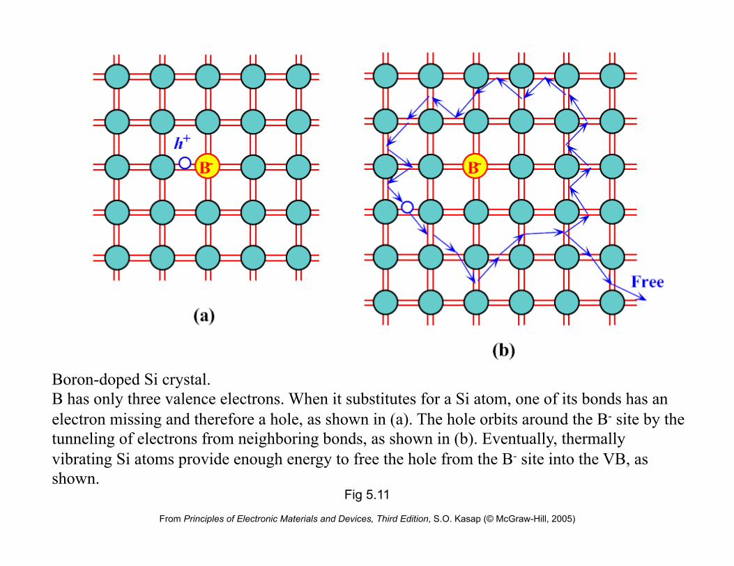
Fig 5.11
From Principles of Electronic Materials and Devices, Third Edition, S.O. Kasap (© McGraw-Hill, 2005)
Boron-doped Si crystal. B has only three valence electrons. When it substitutes for a Si atom, one of its bonds has an electron missing and therefore a hole, as shown in (a). The hole orbits around the B- site by the tunneling of electrons from neighboring bonds, as shown in (b). Eventually, thermally vibrating Si atoms provide enough energy to free the hole from the B- site into the VB, as shown.
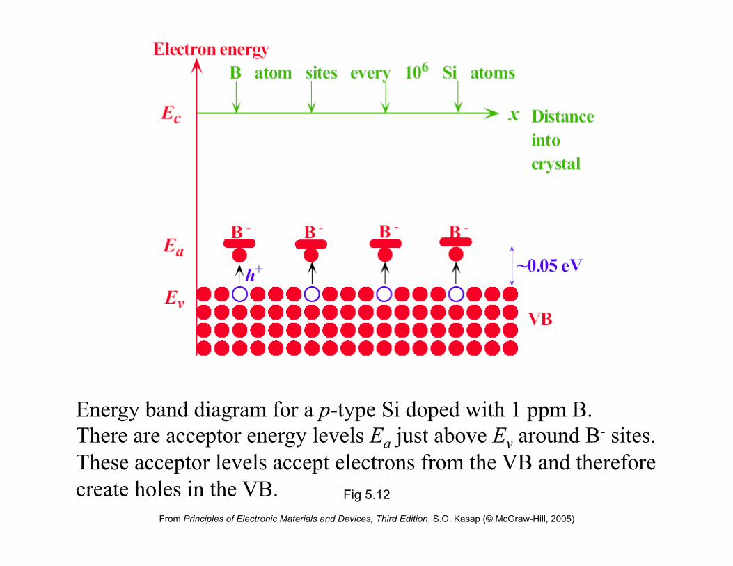
Fig 5.12
From Principles of Electronic Materials and Devices, Third Edition, S.O. Kasap (© McGraw-Hill, 2005)
Energy band diagram for a p-type Si doped with 1 ppm B. There are acceptor energy levels Ea just above Ev around B- sites. These acceptor levels accept electrons from the VB and therefore create holes in the VB.

P-type Conductivity
e = electronic charge Na = acceptor atom concentration in the crystal
µh = hole drift mobility, ni = intrinsic concentration, µe = electron drift mobility
!
" = eNaµh +e ni2
Na
#
$ % %
&
' ( ( µe ) eNaµh
!
" = eNaµh

From Principles of Electronic Materials and Devices, Third Edition, S.O. Kasap (© McGraw-Hill, 2005)
For donors it is energy below CB For acceptors it is energy above VB

Fig 5.13
Energy band diagram of an n-type semiconductor connected to a voltage supply of V volts. The whole energy diagram tilts because the electron now also has an electrostatic potential energy.
Energy band of n-type SC connected to a voltage
Band Bending

From Principles of Electronic Materials and Devices, Third Edition, S.O. Kasap (© McGraw-Hill, 2005)
Compensation Doping
ad NNn −=ad
ii
NNn
nnp
−==
22
iad nNN >>−More donors than acceptors
More acceptors than donors ida nNN >>−
da NNp −=da
ii
NNn
pnn
−==
22

Binding energy of electron in H-atom
!
Eb = "E1 =me
*e4
8#o2h2 = 13.6 eV
!
EbSi =
me*e4
8"o2"r
2h2 = 13.6 eV(me*
me
)( 1"r
2 ) 5.15
!
For Si "r = 11.9 and me*
me=
13
so EbSi # 0.032eV

5.3 Temperature Dependence of Conductivity
3 Regimes: a) kT < Ed b) kT ≈ Ed c) kT >> Ed

Fig 5.14
From Principles of Electronic Materials and Devices, Third Edition, S.O. Kasap (© McGraw-Hill, 2005)
(a) Below Ts, the e-1 conc. is controlled by the ionization of the donors. (b) Between Ts and Ti, the e-1 conc. = concentration of donors since they would all have ionized. (c) At high T, thermally generated electrons from the VB exceed the # # of e-1 from ionized donors and the SC behaves as if intrinsic.

5.3.1 Carrier Concentration
!
n = (12NcNd )1/ 2 exp(" #E
2kT) 5.19
!
n = (NcNv )1/ 2 exp("
Eg2kT
) 5.20
Low Temperature Regime:
Compare to intrinsic case:

Fig 5.15
The temperature dependence of the electron concentration in an n-type semiconductor.
!
n = (12NcNd )1/ 2 exp(" #E
2kT) 5.19
n = Nd (# of donor atoms/m3)
!
n = (NcNv )1/ 2 exp("
Eg2kT
) 5.20

Fig 5.16
From Principles of Electronic Materials and Devices, Third Edition, S.O. Kasap (© McGraw-Hill, 2005)
The temperature dependence of the intrinsic concentration

5.3.2 Drift Mobility and Impurity Dependence
!
µ =e"me
* 5.21
!
" =1
SvthN S 5.22
S is the cross-section area of the scatters, vth = mean speed of electrons, aka as thermal velocity Ns is number of scatters per unit volume.
!
S = "a2
!
12me*vth2 =
32kT

From Principles of Electronic Materials and Devices, Third Edition, S.O. Kasap (© McGraw-Hill, 2005)
!
" L =1
(#a2)vthN S
$ 1(T)(T1/2)
$ T-3/2
Lattice Vibration Scattering Limited Mobility
!
" L # T-3/2 5.23

Scattering of electrons by an ionized impurity.
!
|PE | = ( e2
4"#o#rr)
It is only when KE ≈ PE that electron will get scattered. So
!
3/2kT =|PE(rc ) | = ( e2
4"#o#rrc)
!
S = "rc2 =
"e4
(6"#o#rkT)2 $ T-2
!
rc = e2
6"#o#rkT

!
" L =1
SvthNI # 1
(T-2)(T1/2)NI
# T3/2
NI
µI = ionized impurity scattering limited mobility
!
µI "T 3 / 2
NI 5.24
Ionized Impurity Scattering Limited Mobility

From Principles of Electronic Materials and Devices, Third Edition, S.O. Kasap (© McGraw-Hill, 2005)
Effective or Overall Mobility
µe = effective drift mobility
µI = ionized impurity scattering limited mobility
µL = lattice vibration scattering limited mobility
!
1µe
=1
µI+
1µL
5.25

Log-log plot of drift mobility versus temperature for n-type Ge and n-type Si samples. Various donor concentrations for Si are shown. Nd are in cm-3. The upper right inset is the simple theory for lattice limited mobility, whereas the lower left inset is the simple theory for impurity scattering limited mobility.
Lets look at experimental results. Note LOG-LOG
In English: At the lowest T, increasing the T increases the vth of electrons so as to not be affected by impurities.
BUT , further increases in T causes the atoms to vibrate more and scatter more. So mobility decreases again.
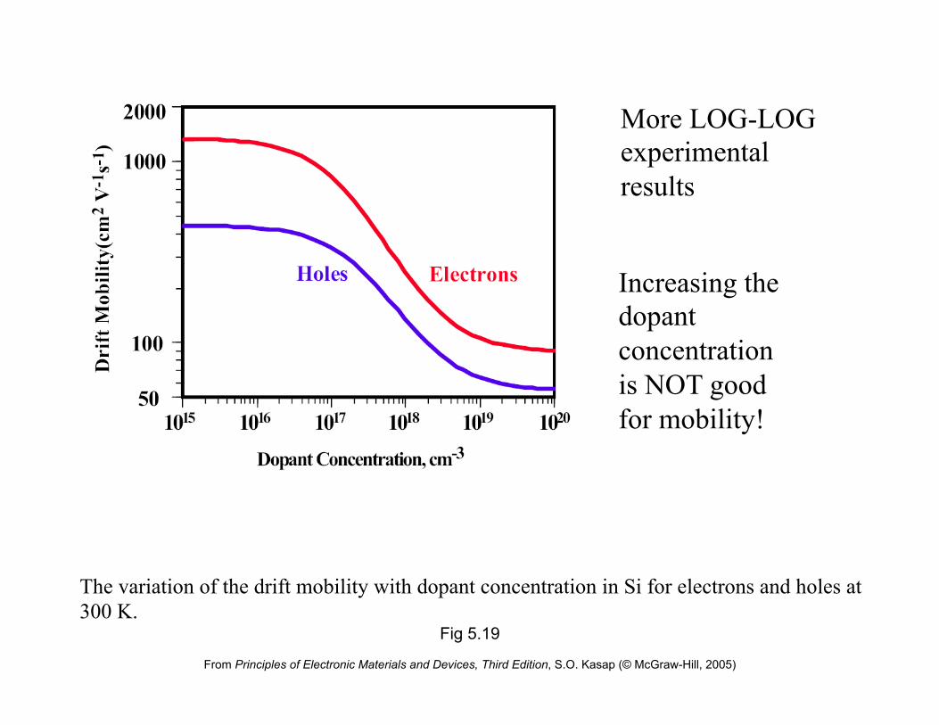
Fig 5.19
From Principles of Electronic Materials and Devices, Third Edition, S.O. Kasap (© McGraw-Hill, 2005)
The variation of the drift mobility with dopant concentration in Si for electrons and holes at 300 K.
More LOG-LOG experimental results
Increasing the dopant concentration is NOT good for mobility!

From Principles of Electronic Materials and Devices, Third Edition, S.O. Kasap (© McGraw-Hill, 2005)
5.3.3 Conductivity Temperature Dependence
OR
Putting it all together
n x µ

Fig 5.20
From Principles of Electronic Materials and Devices, Third Edition, S.O. Kasap (© McGraw-Hill, 2005)
Schematic illustration of the T dependence of electrical conductivity for a doped (n-type) semiconductor.
MISI

In Plain English: For n-type extrinsic SC • At very low temperatures the conductivity is quite low because there are few electrons in the CB. Impurity atoms are holding on to their electrons. • At intermediate temperatures, all the dopant atoms donate their electrons to CB and conductivity saturates. • At very high temperatures, the conductivity is very high because Si-Si bonds are being broken. • Mobilities depend on dopant concentration. For low dopant concentrations mobility is only affected by phonons. • When dopant concentrations are high they can trap electrons at lower temperatures. The trapping probability, however, deceases with increasing T. • All these conclusions apply to p-type SC as well.

Fig 5.21
From Principles of Electronic Materials and Devices, Third Edition, S.O. Kasap (© McGraw-Hill, 2005)
(a) Degenerate n-type SC. Large number of donors form a band that overlaps the CB. (b) Degenerate p-type semiconductor.
Degenerate Semiconductors
You dope the heck out of the SC and end up with an impurity band. Then Boltzmann statistics no longer valid. SC acts as a metal, with ρ α T.

Summary and Conclusions • Intrinsic SC are very poor conductors of
electricity because the density of charge carriers is very small. n = p.
• Doping can dramatically alter the conductivity. Depending on dopant valency, you get either n-type or p-type SC.
• If SC is in thermal equilibrium in the dark
From Principles of Electronic Materials and Devices, Third Edition, S.O. Kasap (© McGraw-Hill, 2005)
!
np = ni2 = NCNVexp(-
Eg
kT)

Summary • For n and p SC, there are 3 regimes of
conductivity – low T = very few carriers, – Intermediate T, saturation; n = Nd and p = Na
– Mobility goes down with increased doping, because dopant attracts the charge carrier slowing it down.
– Like in metals, increasing T, decreases mobility due to scattering by lattice vibrations
From Principles of Electronic Materials and Devices, Third Edition, S.O. Kasap (© McGraw-Hill, 2005)

5.4 Recombination and Minority Carrier Injection
From here on is not included in course. But of you ever get into device physics, it is of crucial importance.

Important concept
• What goes up must come down. Thus at equilibrium, rate of generation of electron-hole pairs must equal rate of recombination of electron-hole pairs!
From Principles of Electronic Materials and Devices, Third Edition, S.O. Kasap (© McGraw-Hill, 2005)

Fig 5.22
Direct recombination in GaAs. kcb = kvb so that momentum conservation is satisfied.
5.4.1 Direct and Indirect Recombination
Direct Recombination:
The states in the VB that can satisfy momentum
conservation, viz. kVB = kCB
are near the top of the VB and the
recombination can occur in a direct fashion.
e.g. GaAs, but NOT Si or Ge.

Fig 5.23
From Principles of Electronic Materials and Devices, Third Edition, S.O. Kasap (© McGraw-Hill, 2005)
Recombination and trapping. (a) Recombination in Si via a recombination center which has a localized energy level at Er in the bandgap, usually near the middle. (b) Trapping and detrapping of electrons by trapping centers. A trapping center has a localized energy level in the band gap.
Recombination center: impurity atom or defect. Electron is captured by RC till a hole shows up and then they combine!
Trapping: permanent removal of e from CB

5.4.2 Minority Carrier Lifetime
nno = majority carrier concentration in thermal equilibrium in the dark
For a n-type semiconductor, n >> p.
pno = minority carrier concentration in thermal equilibrium in the dark
Thermal equilibrium implies:
!
nnopno = ni2 What does ni
depend on????
nn = instantaneous majority carrier concentration
pn = instantaneous minority carrier concentration
∆nn = nn – nno = excess majority carrier concentration
∆pn = pp – pno = excess minority carrier concentration
Same applies for holes

Fig 5.24
From Principles of Electronic Materials and Devices, Third Edition, S.O. Kasap (© McGraw-Hill, 2005)
Low-level photoinjection into an n-type semiconductor in which Δnn > n0
5.4.2 Minority Carrier Lifetime ∆nn = nn – nno
OR: nn = nno + ∆nn
∆pp = pn – pno OR:
pp = pno + ∆pn

Photo-excitation generates equal number of electrons and holes
∆pn = ∆nn
!
dnndt
=d"nndt
and dpndt
=d"pndt

Fig 5.25
From Principles of Electronic Materials and Devices, Third Edition, S.O. Kasap (© McGraw-Hill, 2005)
Low-level injection in an n-type semiconductor does not significantly affect nn but drastically affects the minority carrier concentration pn.
Assume you dope a n-type SC with 5x1016 cm-3
Weak illumination 10% change in n.
∆nn = ∆pn = 0.1 nno
∆nn = ∆pn = 0.5x10¹⁶
pn = pno +∆pn = 2x10³ + 0.5x1016
= 0.5x10¹⁶

Fig 5.26
From Principles of Electronic Materials and Devices, Third Edition, S.O. Kasap (© McGraw-Hill, 2005)
≈
Illumination of an n-type semiconductor results in excess electron and hole concentrations. After the illumination, the recombination process restores equilibrium; the excess electrons and holes simply recombine.

Excess Minority Carrier Concentration
Δpn = excess hole (minority carrier) concentration in n-type
t = time
Gph = rate of photogeneration
τh = minority carrier lifetime (mean recombination time)
GENERAL EQUATION. ONLY ASSUMPTION IS WEAK
INJECTION, ∆pn < nno
!
d"pndt
=Gph #"pn$ h
5.27

From Principles of Electronic Materials and Devices, Third Edition, S.O. Kasap (© McGraw-Hill, 2005)
!
d"pndt
=Gph #"pn$ h
5.27
!
ln[Gph "#pn$ h
] = - t$ h
+ C1
!
"pn (t) = # hGph[1$exp($ t# h
) = 0 < t < toff 5.28
Since at t = 0, ∆pn = 0, C1 = ln Gph
A t t = 0, we turn on light and at t = toff we turn it off.

Now turn light off
• Shows in book that:
From Principles of Electronic Materials and Devices, Third Edition, S.O. Kasap (© McGraw-Hill, 2005)
!
"pn (t' ) = # hGph exp($ t'# h
) for > toff 5.29
Thus one would expect exponential increase and decrease when you turn light on and off.

Fig 5.27
Illumination is switched on at time t = 0 and then off at t= toff. The excess minority carrier concentration Δpn(t) rises exponentially to its steady-state value with a time constant τh. From toff, the excess minority carrier concentration decays exponentially to its equilibrium value.

Fig 5.28
From Principles of Electronic Materials and Devices, Third Edition, S.O. Kasap (© McGraw-Hill, 2005)
A semiconductor slab of length L, width W, and depth D is illuminated with light of Wavelength λ. Iph is the steady-state photocurrent.

From Principles of Electronic Materials and Devices, Third Edition, S.O. Kasap (© McGraw-Hill, 2005)
Change in Conductivity due to Illumination
!
"ph =Ih#
where "ph =# of photons/m2s
!
Gph ="A#ph
AD = "I$
hcD # of EHP/m3s
!
d"ndt
=Gph #"n$
= 0
!
"n = #Gph = #$I%hcD
I = intensity of light = J/m2 s
η = quantum efficiency = # of EHP produced per photon

Fig 5.27
From Principles of Electronic Materials and Devices, Third Edition, S.O. Kasap (© McGraw-Hill, 2005)
!
"# = eµe"n + eµh"p = e"n (µh +µe )!
"n = #Gph = #$I%hcD
!
"# = e$%I&(µe + µh )hcD

5.5 Diffusion and Conduction Equations and Random Motion

From Principles of Electronic Materials and Devices, Third Edition, S.O. Kasap (© McGraw-Hill, 2005)
Definition of Particle Flux
Γ = particle flux, ΔN = number of particles crossing A in a time interval Δt, A = area, Δt = time interval
!
" =#NA#t
Definition of Current Density
J = electric current density, Q = charge of the particle, Γ = particle flux
!
J =Q"

Fig 5.29
From Principles of Electronic Materials and Devices, Third Edition, S.O. Kasap (© McGraw-Hill, 2005)
(a) Arbitrary electron concentration n (x, t) profile in a semiconductor. There is a net diffusion (flux) of electrons from higher to lower concentrations. (b) Expanded view of two adjacent sections at x0. There are more electrons crossing x0 coming From the left (x0-) than coming from the right (x0+)

From Principles of Electronic Materials and Devices, Third Edition, S.O. Kasap (© McGraw-Hill, 2005)
Fick’s First Law
Γe = electron flux, De = diffusion coefficient of electrons, dn/dx = electron concentration gradient
!
"e = #Dedndx
JD, e = electric current density due to electron diffusion, Γe = electron flux, e = electronic charge, De = diffusion coefficient of electrons, dn/dx = electron concentration gradient
Electron Diffusion Current Density
!
JD,e = " e#e = eDedndx

Fig 5.30
From Principles of Electronic Materials and Devices, Third Edition, S.O. Kasap (© McGraw-Hill, 2005)
Arbitrary hole concentration p (x, t) profile in a semiconductor. There is a net diffusion (flux) of holes from higher to lower concentrations. There are more holes crossing x0 coming from the left (x0-) than coming from the right (x0+).

Fig 5.31
From Principles of Electronic Materials and Devices, Third Edition, S.O. Kasap (© McGraw-Hill, 2005)
When there is an electric field and also a concentration gradient, charge carriers move both by diffusion and drift.

From Principles of Electronic Materials and Devices, Third Edition, S.O. Kasap (© McGraw-Hill, 2005)
Hole Diffusion Current Density
JD, h = electric current density due to hole diffusion, e = electronic charge, Γh = hole flux, Dh = diffusion coefficient of holes, dp/dx = hole concentration gradient
!
JD,h = e"h = #eDhdpdx
Total Electron Current Due to Drift and Diffusion
Je = electron current due to drift and diffusion, n = electron concentration, µe = electron drift mobility, Ex = electric field in the x direction, De = diffusion coefficient of electrons, dn/dx = electron concentration gradient
!
Je = enµeE x +eDedndx
5.37

From Principles of Electronic Materials and Devices, Third Edition, S.O. Kasap (© McGraw-Hill, 2005)
Total Hole Current Due to Drift and Diffusion
Jh = hole current due to drift and diffusion, p = hole concentration, µh = hole drift mobility, Ex = electric field in the x direction, Dh = diffusion coefficient of holes, dp/dx = hole concentration gradient
Einstein Relation
De = diffusion coefficient of electrons, µe = electron drift, Dh = diffusion coefficient of the holes, µh = hole drift mobility !
Dh
µh
=kTe
!
De
µe
=kTe
!
Jh = epµhE x "eDhdpdx
5.38

Fig 5.32
From Principles of Electronic Materials and Devices, Third Edition, S.O. Kasap (© McGraw-Hill, 2005)
Nonuniform doping profile results in electron diffusion toward the less concentrated regions. This exposes positively charged donors and sets up a built-in field Ex. In the steady state, the diffusion of electrons toward the right is balanced by their drift toward the left.

From Principles of Electronic Materials and Devices, Third Edition, S.O. Kasap (© McGraw-Hill, 2005)
Built-In Potential and Concentration
V2 = potential at point 2, V1 = potential at point 1, n2 = electron concentration at point 2, n1 = electron concentration at point 1
!
V2 "V1 =kTeln n2
n1
#
$ %
&
' (
Built-In Field in Nonunforim Doping
Ex = electric field in the x direction, k = Boltzmann constant, T = temperature, b = characteristic of the exponential doping profile, e = electronic charge .
!
E x =kTbe

Fig 5.33
From Principles of Electronic Materials and Devices, Third Edition, S.O. Kasap (© McGraw-Hill, 2005)
Consider an elemental volume A δx in which the hole concentration is p(x, t)

From Principles of Electronic Materials and Devices, Third Edition, S.O. Kasap (© McGraw-Hill, 2005)
Continuity Equation for Holes
pn = hole concentration in an n-type semiconductor, pno = equilibrium minority carrier (hole concentration in an n-type semiconductor) concentration, Jh = hole current due to drift and diffusion, τh = hole recombination time (lifetime), Gph = photogeneration rate at x at time t, x = position, t = time
!
"pn"t
= #1e"Jh"x
$
% &
'
( ) #
pn # pno* h
+Gph
Continuity Equation with Uniform Photogeneration
Δpn = pn - pno is the excess hole concentration
!
"#pn"t
= $#pn% h
+Gph

From Principles of Electronic Materials and Devices, Third Edition, S.O. Kasap (© McGraw-Hill, 2005)
Steady-State Continuity Equation for Holes
Jh = hole current due to drift and diffusion, pn = hole concentration in an n-type semiconductor, pno = equilibrium minority carrier (hole concentration in an n-type semiconductor) concentration, τh = hole recombination time (lifetime)
!
1e"Jh"x
#
$ %
&
' ( = )
pn ) pno* h
Steady-State Continuity Equation with E = 0
Δpn = pn - pno is the excess hole concentration, Lh = diffusion length of the holes
!
d2"pndx 2
="pnLh2

Fig 5.34
From Principles of Electronic Materials and Devices, Third Edition, S.O. Kasap (© McGraw-Hill, 2005)
(a) Steady state excess carrier concentration profiles in an n-type semiconductor that is continuously illuminated at one end.
(b) Majority and minority carrier current components in open circuit. Total current is zero.

From Principles of Electronic Materials and Devices, Third Edition, S.O. Kasap (© McGraw-Hill, 2005)
From Principles of Electronic Materials and Devices, Third Edition, S.O. Kasap (© McGraw-Hill, 2005)
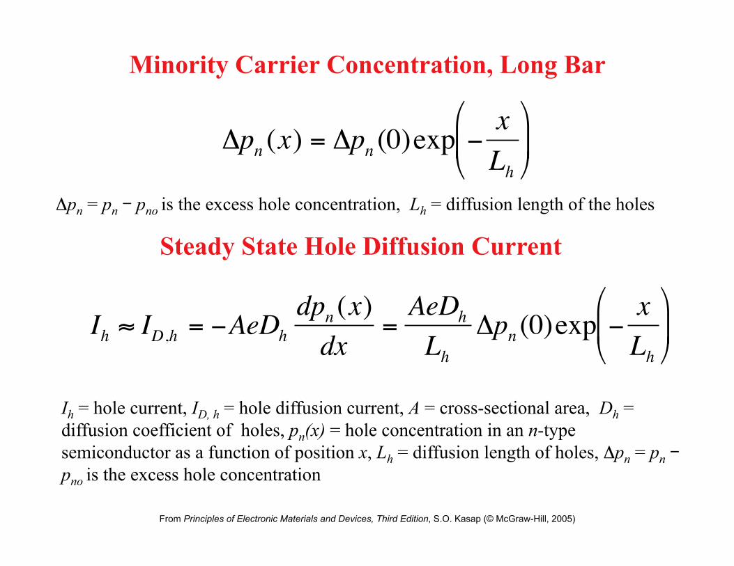
Minority Carrier Concentration, Long Bar
Δpn = pn - pno is the excess hole concentration, Lh = diffusion length of the holes
!
"pn (x) = "pn (0)exp #xLh
$
% &
'
( )
Steady State Hole Diffusion Current
Ih = hole current, ID, h = hole diffusion current, A = cross-sectional area, Dh = diffusion coefficient of holes, pn(x) = hole concentration in an n-type semiconductor as a function of position x, Lh = diffusion length of holes, Δpn = pn - pno is the excess hole concentration !
Ih " ID,h = #AeDhdpn (x)dx
=AeDh
Lh$pn (0)exp #
xLh
%
& '
(
) *

From Principles of Electronic Materials and Devices, Third Edition, S.O. Kasap (© McGraw-Hill, 2005)
Majority Carrier Concentration, Long Bar
Δnn(x) = the excess electron concentration, x = position, Le = diffusion length of the electrons
!
"nn (x) = "nn (0)exp #xLe
$
% &
'
( )
Electron Diffusion Current
ID, e = electron diffusion current, De = diffusion coefficient of electrons, nn(x) = electron concentration in an n-type semiconductor as a function of position x, Le = diffusion length of the electrons, Δnn = the excess electron concentration !
ID,e = AeDednn (x)dx
= "AeDe
Le#nn (0)exp "
xLe
$
% &
'
( )

Summary • Degenerate SC behave like metals and
!
np " ni2
• Direct and indirect recombination • Recombination vs trapping • Minority carrier lifetime, τ. Relaxation of
system scales as the exp (-t/τ). • Electrons and holes drift due to the
combined effects of concentration and potential gradients.

From Principles of Electronic Materials and Devices, Third Edition, S.O. Kasap (© McGraw-Hill, 2005)
Electron Drift Current: Use the Open Circuit Condition
Idrift, e = electron drift current, ID, e = electron diffusion current, ID, h = hole diffusion current,
0,,,drift =++ hDeDe III
Electric Field
E = electric field, Idrift, e = electron drift current, nno = equilibrium majority carrier (electron concentration in an n-type semiconductor) concentration, µe = electron drift mobility
!
E =Idrift,eAennoµe
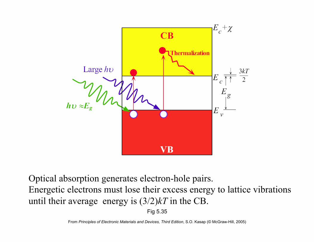
Fig 5.35
From Principles of Electronic Materials and Devices, Third Edition, S.O. Kasap (© McGraw-Hill, 2005)
Optical absorption generates electron-hole pairs. Energetic electrons must lose their excess energy to lattice vibrations until their average energy is (3/2)kT in the CB.

Fig 5.36
From Principles of Electronic Materials and Devices, Third Edition, S.O. Kasap (© McGraw-Hill, 2005)
Absorption of photons within a small elemental volume of width x

From Principles of Electronic Materials and Devices, Third Edition, S.O. Kasap (© McGraw-Hill, 2005)
Definition of Optical Absorption Coefficient
α = absorption coefficient, I = light intensity, δI = change in the light intensity in a small elemental volume of thickness δx at x
!
" = #$II$x
Beer-Lambert Law
I(x) = light intensity at x, Io = initial light intensity, α = absorption coefficient, x = distance from the surface (location) where I = Io. Note: Light propagates along x.
!
I(x) = Io exp("#x)

Fig 5.37
From Principles of Electronic Materials and Devices, Third Edition, S.O. Kasap (© McGraw-Hill, 2005)
The absorption coefficient α depends on the photon energy hν and hence on the wavelength. Density of states increases from band edges and usually exhibits peaks and troughs. Generally α increases with the photon energy greater than Eg because more energetic photons can excite electrons from populated regions of the VB to numerous available states deep in the CB.

Fig 5.38
From Principles of Electronic Materials and Devices, Third Edition, S.O. Kasap (© McGraw-Hill, 2005)
Piezoresistivity and its applications. (a) Stress σm along the current (longitudinal) direction changes the resistivity by δρ. (b) Stresses σL and σT cause a resistivity change. (c) A force applied to a cantilever bends it. A piezoresistor at the support end (where the stress is large) measures the stress, which is proportional to the force.
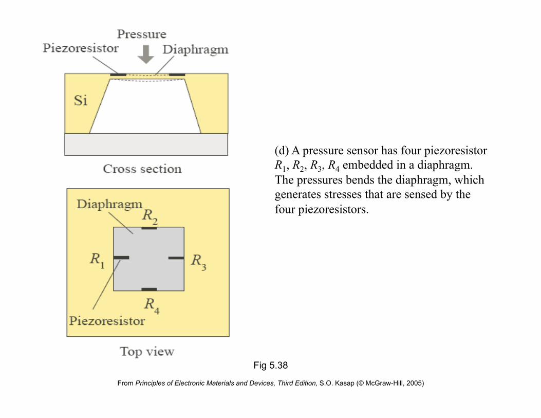
Fig 5.38
From Principles of Electronic Materials and Devices, Third Edition, S.O. Kasap (© McGraw-Hill, 2005)
(d) A pressure sensor has four piezoresistor R1, R2, R3, R4 embedded in a diaphragm. The pressures bends the diaphragm, which generates stresses that are sensed by the four piezoresistors.

Fig 5.39
From Principles of Electronic Materials and Devices, Third Edition, S.O. Kasap (© McGraw-Hill, 2005)
Formation of a Schottky junction between a metal and an n-type semiconductor when Φm > Φn.

From Principles of Electronic Materials and Devices, Third Edition, S.O. Kasap (© McGraw-Hill, 2005)
Schottky Junction: Metal to n-Type Semiconductor
Barrier height ΦB from the metal to the semiconductor
ΦB = Φm – χ = eVo + (Ec – EFn)
eVo = Φm = Φn
Work function of metal
Electron affinity of the semiconductors Built-in potential
Distance of Fermi level from CB in the semiconductor
Work function of the semiconductor
Built-in potential Vo
Work function of the metal

Fig 5.40
From Principles of Electronic Materials and Devices, Third Edition, S.O. Kasap (© McGraw-Hill, 2005)
The Schotkky Junction

From Principles of Electronic Materials and Devices, Third Edition, S.O. Kasap (© McGraw-Hill, 2005)
Schottky Junction
J = current density
Jo = constant that depends on the metal and the semiconductor
e.g. ΦB, Vo, and also on the surface properties
V = voltage, e = electronic charge
k = Boltzmann constant, T = temperature
⎥⎦
⎤⎢⎣
⎡−⎟⎠
⎞⎜⎝
⎛= 1expkTeVJJ o

Fig 5.41
From Principles of Electronic Materials and Devices, Third Edition, S.O. Kasap (© McGraw-Hill, 2005)
The principle of the Schottky junction solar cell.

Fig 5.42
From Principles of Electronic Materials and Devices, Third Edition, S.O. Kasap (© McGraw-Hill, 2005)
Reverse biased Schottky photodiodes are frequently used as fast photodetectors.

Fig 5.43
From Principles of Electronic Materials and Devices, Third Edition, S.O. Kasap (© McGraw-Hill, 2005)
When a metal with a smaller workfunction than an n-type semiconductor are put into contact, The resulting junction is an ohmic contact in the sense that it does not limit the current flow.

Fig 5.44
From Principles of Electronic Materials and Devices, Third Edition, S.O. Kasap (© McGraw-Hill, 2005)
(a) Current from an n-type semiconductor to the metal results in heat absorption at the junction. (b) Current from the metal to an n-type semiconductor results in heat release at the junction.

Fig 5.45
From Principles of Electronic Materials and Devices, Third Edition, S.O. Kasap (© McGraw-Hill, 2005)
When a dc current is passed through a semiconductor to which metal contacts have been made, one junction absorbs heat and cools (the cold junction) and the other releases heat and warms (the hot junction).

Fig 5.46
From Principles of Electronic Materials and Devices, Third Edition, S.O. Kasap (© McGraw-Hill, 2005)
Cross section of a typical thermoelectric cooler.

Fig 5.47
From Principles of Electronic Materials and Devices, Third Edition, S.O. Kasap (© McGraw-Hill, 2005)
Typical structure of a commercial thermoelectric cooler.

From Principles of Electronic Materials and Devices, Third Edition, S.O. Kasap (© McGraw-Hill, 2005)

Fig 5.48
From Principles of Electronic Materials and Devices, Third Edition, S.O. Kasap (© McGraw-Hill, 2005)
The electron PE, V(x), inside the crystal is periodic with the same periodicity as that of the Crystal, a. Far away outside the crystal, by choice, V = 0 (the electron is free and PE = 0).
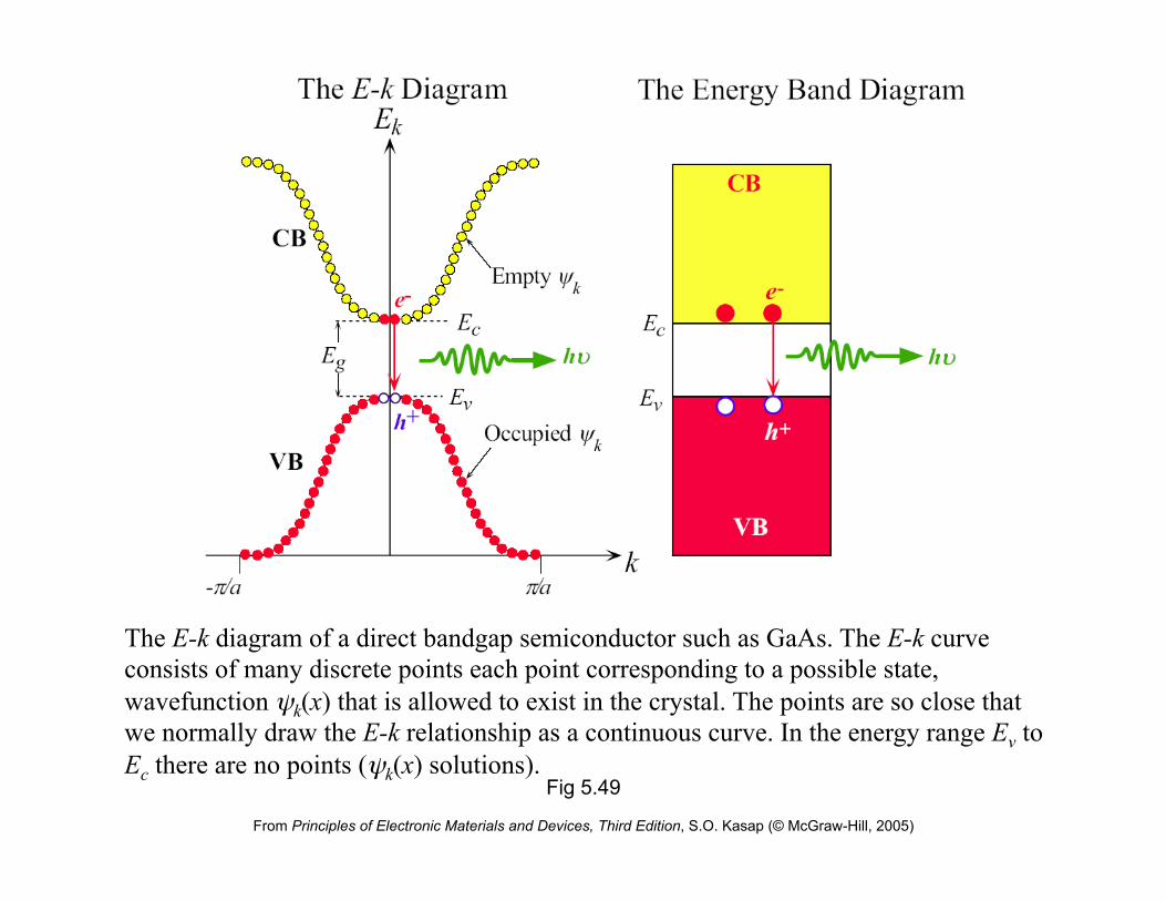
Fig 5.49
From Principles of Electronic Materials and Devices, Third Edition, S.O. Kasap (© McGraw-Hill, 2005)
The E-k diagram of a direct bandgap semiconductor such as GaAs. The E-k curve consists of many discrete points each point corresponding to a possible state, wavefunction ψk(x) that is allowed to exist in the crystal. The points are so close that we normally draw the E-k relationship as a continuous curve. In the energy range Ev to Ec there are no points (ψk(x) solutions).

Fig 5.50
From Principles of Electronic Materials and Devices, Third Edition, S.O. Kasap (© McGraw-Hill, 2005)
(a) In GaAs the minimum of the CB is directly above the maximum of the VB. GaAs is therefore a direct band gap semiconductor. (b) In Si, the minimum of the CB is displaced from the maximum of the VB and Si is an indirect band gap semiconductor. (c) Recombination of an electron and a hole in Si involves a recombination center.

Fig 5.51
From Principles of Electronic Materials and Devices, Third Edition, S.O. Kasap (© McGraw-Hill, 2005)
(a) In the absence of a field, over a long time, average of all k values is zero, there is no net momentum in any one direction. (b) In the presence of a field E in the –x direction, the electron accelerates in the +x direction increasing its k value along x until it is scattered to a random k value. Over a long time, average of all k values is along the +x direction. Thus the electron drifts along +x.

From Principles of Electronic Materials and Devices, Third Edition, S.O. Kasap (© McGraw-Hill, 2005)
Electron’s group velocity
vg = group velocity, E = electron energy, k = electron’s wavevector
!
vg =1!dEdk
External force and acceleration
Fext = externally applied force, a = acceleration
!
Fext =!2
d2Edk 2
"
# $
%
& '
a
From Principles of Electronic Materials and Devices, Third Edition, S.O. Kasap (© McGraw-Hill, 2005)
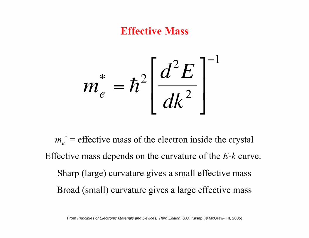
Effective Mass
me* = effective mass of the electron inside the crystal
Effective mass depends on the curvature of the E-k curve.
Sharp (large) curvature gives a small effective mass
Broad (small) curvature gives a large effective mass
!
me* = !2
d2Edk 2
"
# $
%
& '
(1

Fig 5.52
From Principles of Electronic Materials and Devices, Third Edition, S.O. Kasap (© McGraw-Hill, 2005)
(a) In a full valence band there is no net contribution to the current. There are equal numbers of electrons (e.g. at b and b') with opposite momenta. (b) If there is an empty state (hole) at b at the top of the band then the electron at b' contributes to the current.

Fig 5.53
From Principles of Electronic Materials and Devices, Third Edition, S.O. Kasap (© McGraw-Hill, 2005)
Schematic representation of the density of states g(E) vs. energy E for an amorphous semiconductor and the associated electron wavefunctions for an electron in the extended and localized states.

Fig 5.54
From Principles of Electronic Materials and Devices, Third Edition, S.O. Kasap (© McGraw-Hill, 2005)
The GaAs crystal structure in two dimensions. Average number of valence electrons per atom is four. Each Ga atom covalently bonds with four neighboring As atoms and vice versa.

From Principles of Electronic Materials and Devices, Third Edition, S.O. Kasap (© McGraw-Hill, 2005)
From Principles of Electronic Materials and Devices, Third Edition, S.O. Kasap (© McGraw-Hill, 2005)

From Principles of Electronic Materials and Devices, Third Edition, S.O. Kasap (© McGraw-Hill, 2005)

Fig 5.55
From Principles of Electronic Materials and Devices, Third Edition, S.O. Kasap (© McGraw-Hill, 2005)
In the presence of a temperature gradient, there is an internal field and a voltage difference. The Seebeck coefficient is defined as dV/dT, the potential difference per unit temperature difference.
Related Documents