9-1 Chapter 9 Metrology Methods for Ion Implantation Process Controls Michael Current Current Scientific, San Jose, CA USA [email protected] New metrology tools have been developed for characterization of shallow (≈10 nm) and deep (2 to 10 um) junctions as well as to map dose and annealing variations on test wafers at sub-mm resolution. Well-established tools, in particular 4-point probes (4PP), have been extended with the development of “elastic material” probe t ips and MEMS- based micro-4PP with micron scale probe spacing. Surface resistivity probes, coupled with AFM scanning methods, now provide 2D device maps with nm scale resolution. New physical methods include junction imaging with holographic-TEM and atom-by- atom chemical analysis of device structures by field evaporation atom probes that provide 2D and 3D maps of IC devices. And new types of optical, based on reflectivity and photoluminescence, and photo-voltage measurements provide non-contact tools sensitivity to details of dopant and damage distributions as well as electrical measurements of sheet resistance and carrier recombination leakage currents. Chapter Outline 1. Metrology challenges for doping applications: 9-2 2. Electrical methods: 4-Point Probe (4PP) 9-3 micro-4-Point Probe (micro 4PP) 9-6 Active Surface Dopant levels (N surf ) 9-10 Scanning Spreading Resistance Microscopy (SSRM). 9-11 3. Photo-Voltaic (PV) Methods: Surface Charge 9-15 Carrier Spreading Sheet Resistance (RsL) 9-8 4. Optical methods: Modulated Optical Reflectance (MOR) 9-24 Photo-Luminescence (PL) 9-27 5. 2D & 3D Physical Methods: Holography (3D Image) with TEM (holo-TEM) 9-30 Atom Probe Tomography (APT) 9-32 6. Summary: 9-36 References: 9-37

Ch 09 - Metrology - Current IIT12
Oct 27, 2014
Welcome message from author
This document is posted to help you gain knowledge. Please leave a comment to let me know what you think about it! Share it to your friends and learn new things together.
Transcript

9-1
Chapter 9
Metrology Methods for Ion Implantation
Process Controls
Michael Current Current Scientific, San Jose, CA USA
New metrology tools have been developed for characterization of shallow (≈10 nm) and
deep (2 to 10 um) junctions as well as to map dose and annealing variations on test
wafers at sub-mm resolution. Well-established tools, in particular 4-point probes (4PP),
have been extended with the development of “elastic material” probe tips and MEMS-
based micro-4PP with micron scale probe spacing. Surface resistivity probes, coupled
with AFM scanning methods, now provide 2D device maps with nm scale resolution.
New physical methods include junction imaging with holographic-TEM and atom-by-
atom chemical analysis of device structures by field evaporation atom probes that provide
2D and 3D maps of IC devices. And new types of optical, based on reflectivity and
photoluminescence, and photo-voltage measurements provide non-contact tools
sensitivity to details of dopant and damage distributions as well as electrical
measurements of sheet resistance and carrier recombination leakage currents.
Chapter Outline
1. Metrology challenges for doping applications: 9-2
2. Electrical methods:
4-Point Probe (4PP) 9-3
micro-4-Point Probe (micro 4PP) 9-6
Active Surface Dopant levels (Nsurf) 9-10
Scanning Spreading Resistance Microscopy (SSRM). 9-11
3. Photo-Voltaic (PV) Methods:
Surface Charge 9-15
Carrier Spreading Sheet Resistance (RsL) 9-8
4. Optical methods:
Modulated Optical Reflectance (MOR) 9-24
Photo-Luminescence (PL) 9-27
5. 2D & 3D Physical Methods:
Holography (3D Image) with TEM (holo-TEM) 9-30
Atom Probe Tomography (APT) 9-32
6. Summary: 9-36
References: 9-37
9-2
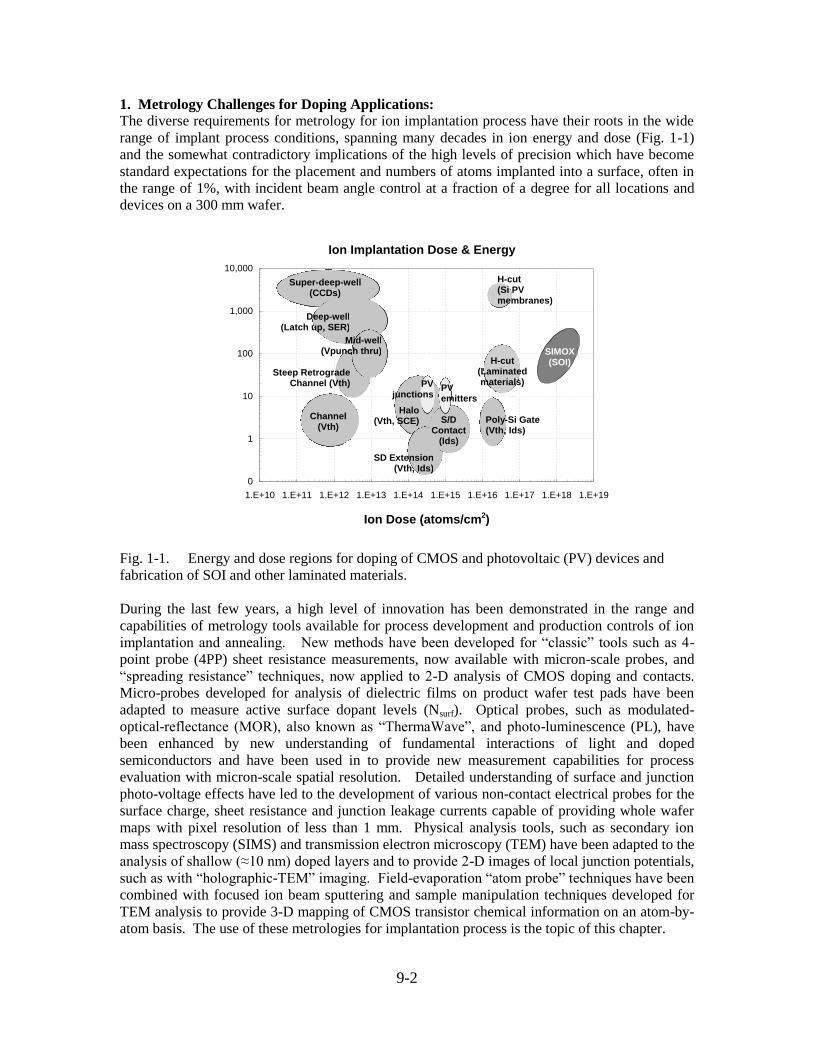
1. Metrology Challenges for Doping Applications: The diverse requirements for metrology for ion implantation process have their roots in the wide
range of implant process conditions, spanning many decades in ion energy and dose (Fig. 1-1)
and the somewhat contradictory implications of the high levels of precision which have become
standard expectations for the placement and numbers of atoms implanted into a surface, often in
the range of 1%, with incident beam angle control at a fraction of a degree for all locations and
devices on a 300 mm wafer.
Fig. 1-1. Energy and dose regions for doping of CMOS and photovoltaic (PV) devices and
fabrication of SOI and other laminated materials.
During the last few years, a high level of innovation has been demonstrated in the range and
capabilities of metrology tools available for process development and production controls of ion
implantation and annealing. New methods have been developed for “classic” tools such as 4-
point probe (4PP) sheet resistance measurements, now available with micron-scale probes, and
“spreading resistance” techniques, now applied to 2-D analysis of CMOS doping and contacts.
Micro-probes developed for analysis of dielectric films on product wafer test pads have been
adapted to measure active surface dopant levels (Nsurf). Optical probes, such as modulated-
optical-reflectance (MOR), also known as “ThermaWave”, and photo-luminescence (PL), have
been enhanced by new understanding of fundamental interactions of light and doped
semiconductors and have been used in to provide new measurement capabilities for process
evaluation with micron-scale spatial resolution. Detailed understanding of surface and junction
photo-voltage effects have led to the development of various non-contact electrical probes for the
surface charge, sheet resistance and junction leakage currents capable of providing whole wafer
maps with pixel resolution of less than 1 mm. Physical analysis tools, such as secondary ion
mass spectroscopy (SIMS) and transmission electron microscopy (TEM) have been adapted to the
analysis of shallow (≈10 nm) doped layers and to provide 2-D images of local junction potentials,
such as with “holographic-TEM” imaging. Field-evaporation “atom probe” techniques have been
combined with focused ion beam sputtering and sample manipulation techniques developed for
TEM analysis to provide 3-D mapping of CMOS transistor chemical information on an atom-by-
atom basis. The use of these metrologies for implantation process is the topic of this chapter.
Ion Implantation Dose & Energy
0
1
10
100
1,000
10,000
1.E+10 1.E+11 1.E+12 1.E+13 1.E+14 1.E+15 1.E+16 1.E+17 1.E+18 1.E+19
Ion Dose (atoms/cm2)
Ato
m E
ne
rgy
(k
eV
)
Channel(Vth)
Steep Retrograde Channel (Vth)
Mid-well(Vpunch thru)
Deep-well(Latch up, SER)
Super-deep-well(CCDs)
H-cut(Laminatedmaterials)
Halo(Vth, SCE)
SD Extension(Vth, Ids)
S/D Contact
(Ids)
Poly-Si Gate(Vth, Ids)
H-cut(Si PV membranes)
SIMOX(SOI)
PV junctions
PV emitters
9-3
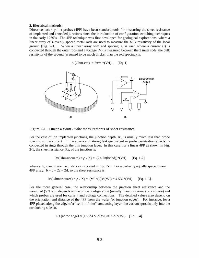
2. Electrical methods: Direct contact 4-poiint probes (4PP) have been standard tools for measuring the sheet resistance
of implanted and annealed junctions since the introduction of configuration switching techniques
in the early 1980’s. The 4PP technique was first developed for geological explorations, where a
linear array of 4 evenly spaced metal rods are used to measure the bulk resistivity of the local
ground (Fig. 2-1). When a linear array with rod spacing, s, is used where a current (I) is
conducted through the outer rods and a voltage (V) is measured between the 2 inner rods, the bulk
resistivity of the ground (assumed to be much thicker than the rod spacing) is:
(Ohm-cm) = 2*s *(V/I). [Eq. 1]
Figure 2-1. Linear 4 Point Probe measurements of sheet resistance.
For the case of ion implanted junctions, the junction depth, Xj, is usually much less than probe
spacing, so the current (in the absence of strong leakage current or probe penetration effects) is
conducted in rings through the thin junction layer. In this case, for a linear 4PP as shown in Fig.
2-1, the sheet resistance, Rs, of the junction is:
Rs(Ohms/square) = / Xj = (2/ ln(bc/ad))*(V/I) [Eq. 1-2]
where a, b, c and d are the distances indicated in Fig. 2-1. For a perfectly equally spaced linear
4PP array, b = c = 2a = 2d, so the sheet resistance is:
Rs(Ohms/square) = / Xj = (/ ln(2))*(V/I) = 4.532*(V/I) [Eq. 1-3].
For the more general case, the relationship between the junction sheet resistance and the
measured (V/I ratio depends on the probe configuration (usually linear or corners of a square) and
which probes are used for current and voltage connections. The detailed values also depend on
the orientation and distance of the 4PP from the wafer (or junction edges). For instance, for a
4PP placed along the edge of a “semi-infinite” conducting layer, the current spreads only into the
conducting side so,
Rs (at the edge) ≈ (1/2)*4.53*(V/I) ≈ 2.27*(V/I) [Eq. 1-4].
9-4
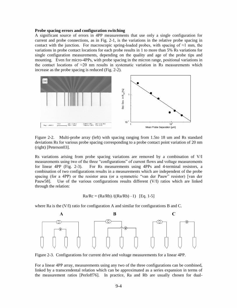
Probe spacing errors and configuration switching
A significant source of errors in 4PP measurements that use only a single configuration for
current and probe connections, as in Fig. 2-1, is the variations in the relative probe spacing in
contact with the junction. For macroscopic spring-loaded probes, with spacing of ≈1 mm, the
variations in probe contact locations for each probe results in 1 to more than 5% Rs variations for
single configuration measurements, depending on the quality and age of the probe tips and
mounting. Even for micro-4PPs, with probe spacing in the micron range, positional variations in
the contact locations of ≈20 nm results in systematic variation in Rs measurements which
increase as the probe spacing is reduced (Fig. 2-2).
Figure 2-2. Multi-probe array (left) with spacing ranging from 1.5to 18 um and Rs standard
deviations Rs for various probe spacing corresponding to a probe contact point variation of 20 nm
(right) [Peterson03].
Rs variations arising from probe spacing variations are removed by a combination of V/I
measurements using two of the three “configurations” of current flows and voltage measurements
for linear 4PP (Fig. 2-3). For Rs measurements using 4PPs and 4-terminal resistors, a
combination of two configurations results in a measurements which are independent of the probe
spacing (for a 4PP) or the resistor area (or a symmetric “van der Pauw” resistor) [van der
Pauw58]. Use of the various configurations results different (V/I) ratios which are linked
through the relation:
Ra/Rc = (Ra/Rb) /((Ra/Rb) –1) [Eq. 1-5]
where Ra is the (V/I) ratio for configuration A and similar for configurations B and C.
Figure 2-3. Configurations for current drive and voltage measurements for a linear 4PP.
For a linear 4PP array, measurements using any two of the three configurations can be combined,
linked by a transcendental relation which can be approximated as a series expansion in terms of
the measurement ratios [Perloff76]. In practice, Ra and Rb are usually chosen for dual-
9-5
configuration measurements since they have comparable magnitudes and have higher voltage
signals than Rc. A good approximation for Ka is:
Ka = -14.696 + 25.173(Ra/Rb) – 7.872 ((Ra/Rb)2 [Eq. 1-6]
where Rs = Ka*Ra. The value of ka ranges on both sides of the value of 4.532 for the ideal case
of an equally spaced 4PP array (Fig. 2-4).
Figure 2-4. Proportionality factor linking Ra, the (V/I) ratio measured using configuration A, to
the junction sheet resistance, Rs, when using measurements from configurations A and B (see
Fig. 2-3). The factor of /ln2 ≈ 4.532 is for an ideal 4PP, with equally spaced probe locations.
The use of dual-configuration 4PP measurements not only reduces the errors due to variable
probe spacing to <0.1% but also relaxes the requirements for probe orientation (usually solved for
the case of a linear probe array aligned along the wafer radius) and reduces the distance over
which wafer edge corrections become important (usually ≈5x the probe spacing for a 0.1% error).
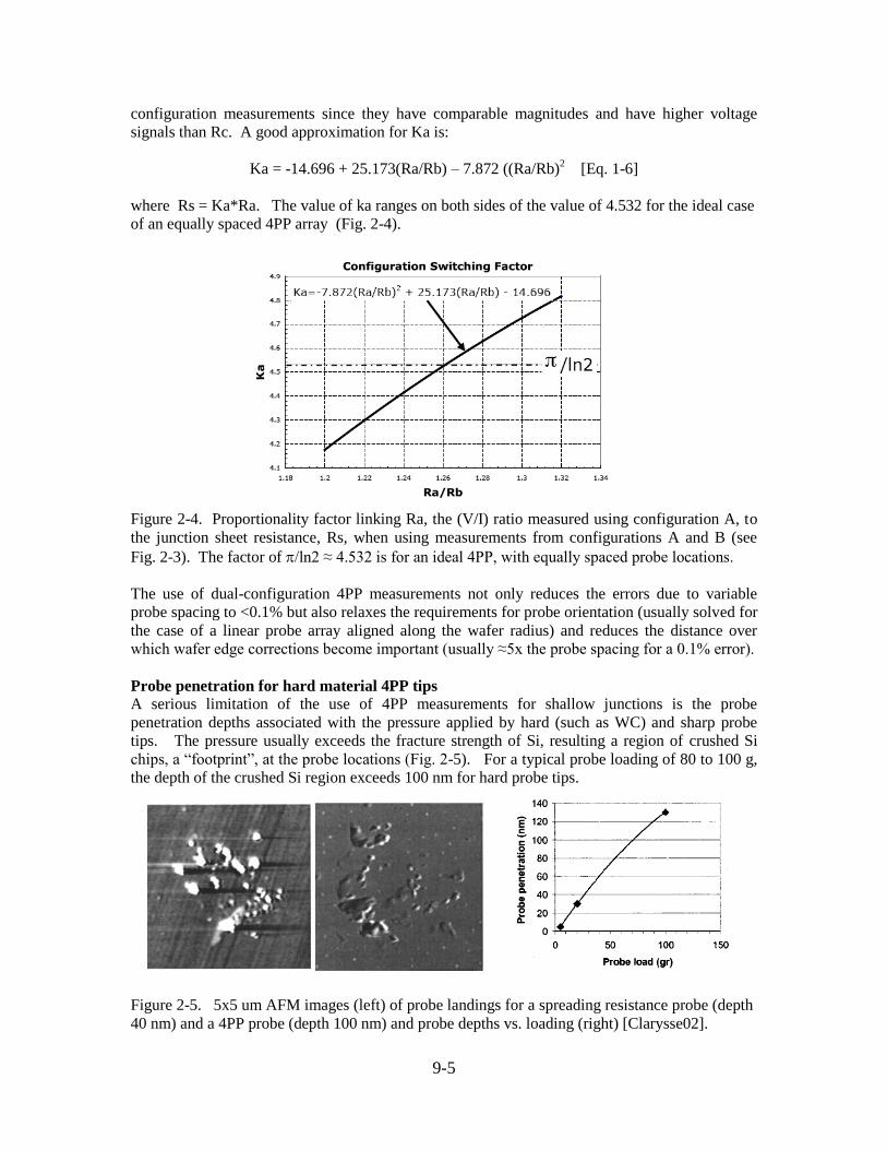
Probe penetration for hard material 4PP tips A serious limitation of the use of 4PP measurements for shallow junctions is the probe
penetration depths associated with the pressure applied by hard (such as WC) and sharp probe
tips. The pressure usually exceeds the fracture strength of Si, resulting a region of crushed Si
chips, a “footprint”, at the probe locations (Fig. 2-5). For a typical probe loading of 80 to 100 g,
the depth of the crushed Si region exceeds 100 nm for hard probe tips.
Figure 2-5. 5x5 um AFM images (left) of probe landings for a spreading resistance probe (depth
40 nm) and a 4PP probe (depth 100 nm) and probe depths vs. loading (right) [Clarysse02].

9-6
Micro-4PP arrays
The penetration of hard materials probe tips for shallow junctions has led to the use of “soft”
probe tip materials (such as Hg and elastically-deformable metals) and the development of probes
with significantly lower probe contact force. The application of semiconductor-MEMS based
fabrication procedures has resulted in probe tip spacing on the order of 10s of um (see Figs. 2-2
and 2.6) [Petersen08]. The probe tip materials are Si or SiO2 coated with thin metal (Ni or Au)
skins and contacted to junctions with pressures on the order of 10-5
N (≈0.3 mg load on contact
size of 50-100 nm).
Figure 2-6. SEM images of a micro-4PP with spacing of 20 um.
The use of micro-4PPs results in minimal probe penetration (allowing accurate measurements for
≈10 nm junctions), reduced sensitivity to leakage current errors (both effects discussed later) and
minimized edge correction distances of much less than 1 mm. The principal advantage of the use
of micron-scale micro-4PPs is the high spatial resolution of local sheet resistance variations due
to local dopant (due to implant) or activation (due to annealing) non-uniformities (Fig. 2-7).
Figure 2-7. Rs values for line scans (left) with various spacing micro-4PPs measured (in 25 um
steps) perpendicular to a multi-pass laser anneal scan direction and a 45x101 point map (right) of
a laser annealed region using a 10 um 4PP spacing with step sizes of 50 um (x-direction) and 250
um (y-direction) [Petersen08]. Note the larger measured Rs variations in the line scans for the
smaller probe spacings and the complexity of the local Rs variation pattern in the map (laser scan
direction is in the x-direction).
9-7
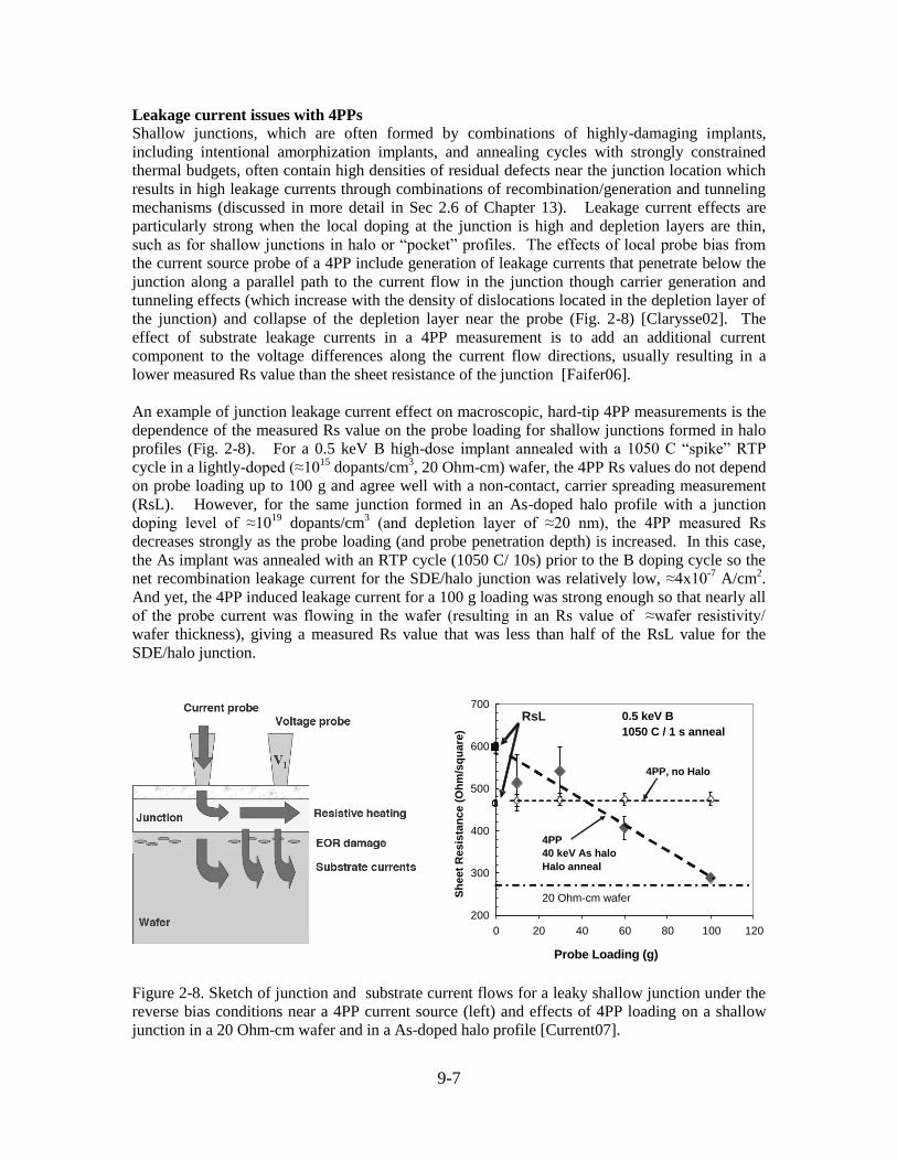
Leakage current issues with 4PPs
Shallow junctions, which are often formed by combinations of highly-damaging implants,
including intentional amorphization implants, and annealing cycles with strongly constrained
thermal budgets, often contain high densities of residual defects near the junction location which
results in high leakage currents through combinations of recombination/generation and tunneling
mechanisms (discussed in more detail in Sec 2.6 of Chapter 13). Leakage current effects are
particularly strong when the local doping at the junction is high and depletion layers are thin,
such as for shallow junctions in halo or “pocket” profiles. The effects of local probe bias from
the current source probe of a 4PP include generation of leakage currents that penetrate below the
junction along a parallel path to the current flow in the junction though carrier generation and
tunneling effects (which increase with the density of dislocations located in the depletion layer of
the junction) and collapse of the depletion layer near the probe (Fig. 2-8) [Clarysse02]. The
effect of substrate leakage currents in a 4PP measurement is to add an additional current
component to the voltage differences along the current flow directions, usually resulting in a
lower measured Rs value than the sheet resistance of the junction [Faifer06].
An example of junction leakage current effect on macroscopic, hard-tip 4PP measurements is the
dependence of the measured Rs value on the probe loading for shallow junctions formed in halo
profiles (Fig. 2-8). For a 0.5 keV B high-dose implant annealed with a 1050 C “spike” RTP
cycle in a lightly-doped (≈1015
dopants/cm3, 20 Ohm-cm) wafer, the 4PP Rs values do not depend
on probe loading up to 100 g and agree well with a non-contact, carrier spreading measurement
(RsL). However, for the same junction formed in an As-doped halo profile with a junction
doping level of ≈1019
dopants/cm3 (and depletion layer of ≈20 nm), the 4PP measured Rs
decreases strongly as the probe loading (and probe penetration depth) is increased. In this case,
the As implant was annealed with an RTP cycle (1050 C/ 10s) prior to the B doping cycle so the
net recombination leakage current for the SDE/halo junction was relatively low, ≈4x10⁻⁷
A/cm2.
And yet, the 4PP induced leakage current for a 100 g loading was strong enough so that nearly all
of the probe current was flowing in the wafer (resulting in an Rs value of ≈wafer resistivity/
wafer thickness), giving a measured Rs value that was less than half of the RsL value for the
SDE/halo junction.
Figure 2-8. Sketch of junction and substrate current flows for a leaky shallow junction under the
reverse bias conditions near a 4PP current source (left) and effects of 4PP loading on a shallow
junction in a 20 Ohm-cm wafer and in a As-doped halo profile [Current07].
200
300
400
500
600
700
0 20 40 60 80 100 120
Probe loading (g)
Sh
ee
t R
es
ista
nc
e (
Oh
m/s
qu
are
)
20 Ohm-cm wafer
RsL
4PP
40 keV As halo
Halo anneal
0.5 keV B
1050 C / 1 s anneal
4PP, no Halo
Probe Loading (g)
9-8
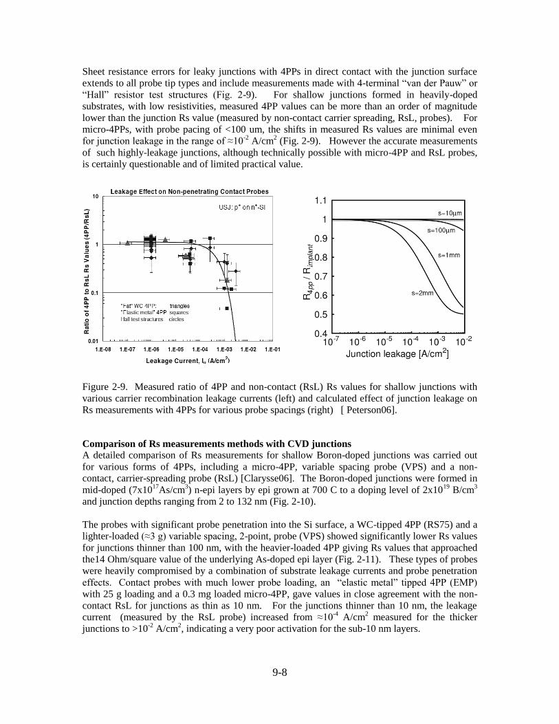
Sheet resistance errors for leaky junctions with 4PPs in direct contact with the junction surface
extends to all probe tip types and include measurements made with 4-terminal “van der Pauw” or
“Hall” resistor test structures (Fig. 2-9). For shallow junctions formed in heavily-doped
substrates, with low resistivities, measured 4PP values can be more than an order of magnitude
lower than the junction Rs value (measured by non-contact carrier spreading, RsL, probes). For
micro-4PPs, with probe pacing of <100 um, the shifts in measured Rs values are minimal even
for junction leakage in the range of ≈10-2
A/cm2 (Fig. 2-9). However the accurate measurements
of such highly-leakage junctions, although technically possible with micro-4PP and RsL probes,
is certainly questionable and of limited practical value.
Figure 2-9. Measured ratio of 4PP and non-contact (RsL) Rs values for shallow junctions with
various carrier recombination leakage currents (left) and calculated effect of junction leakage on
Rs measurements with 4PPs for various probe spacings (right) [ Peterson06].
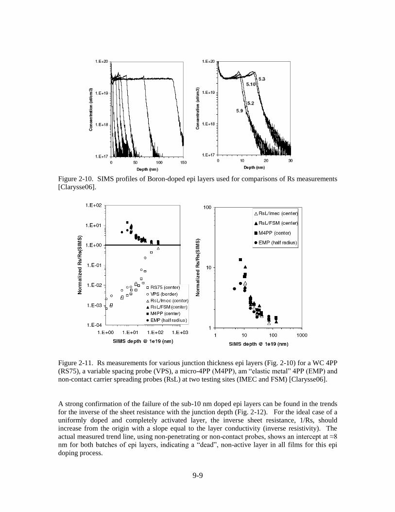
Comparison of Rs measurements methods with CVD junctions A detailed comparison of Rs measurements for shallow Boron-doped junctions was carried out
for various forms of 4PPs, including a micro-4PP, variable spacing probe (VPS) and a non-
contact, carrier-spreading probe (RsL) [Clarysse06]. The Boron-doped junctions were formed in
mid-doped (7x10¹⁷
As/cm3) n-epi layers by epi grown at 700 C to a doping level of 2x10
19 B/cm
3
and junction depths ranging from 2 to 132 nm (Fig. 2-10).
The probes with significant probe penetration into the Si surface, a WC-tipped 4PP (RS75) and a
lighter-loaded (≈3 g) variable spacing, 2-point, probe (VPS) showed significantly lower Rs values
for junctions thinner than 100 nm, with the heavier-loaded 4PP giving Rs values that approached
the14 Ohm/square value of the underlying As-doped epi layer (Fig. 2-11). These types of probes
were heavily compromised by a combination of substrate leakage currents and probe penetration
effects. Contact probes with much lower probe loading, an “elastic metal” tipped 4PP (EMP)
with 25 g loading and a 0.3 mg loaded micro-4PP, gave values in close agreement with the non-
contact RsL for junctions as thin as 10 nm. For the junctions thinner than 10 nm, the leakage
current (measured by the RsL probe) increased from ≈10-4
A/cm2 measured for the thicker
junctions to >10-2
A/cm2, indicating a very poor activation for the sub-10 nm layers.
9-9
Figure 2-10. SIMS profiles of Boron-doped epi layers used for comparisons of Rs measurements
[Clarysse06].
Figure 2-11. Rs measurements for various junction thickness epi layers (Fig. 2-10) for a WC 4PP
(RS75), a variable spacing probe (VPS), a micro-4PP (M4PP), am “elastic metal” 4PP (EMP) and
non-contact carrier spreading probes (RsL) at two testing sites (IMEC and FSM) [Clarysse06].
A strong confirmation of the failure of the sub-10 nm doped epi layers can be found in the trends
for the inverse of the sheet resistance with the junction depth (Fig. 2-12). For the ideal case of a
uniformly doped and completely activated layer, the inverse sheet resistance, 1/Rs, should
increase from the origin with a slope equal to the layer conductivity (inverse resistivity). The
actual measured trend line, using non-penetrating or non-contact probes, shows an intercept at ≈8
nm for both batches of epi layers, indicating a “dead”, non-active layer in all films for this epi
doping process.
9-10
Figure 2-12. Inverse sheet resistance vs. junction depth for two batches of epi-doped layers using
non-penetrating or non-contact probes. The “SIMS” points are for complete activation of the
dopant atom profile. Note the intercept at ≈8 nm in the Rs data, indicating a non-active layer,
approximately 8 nm thick, for all epi thicknesses.
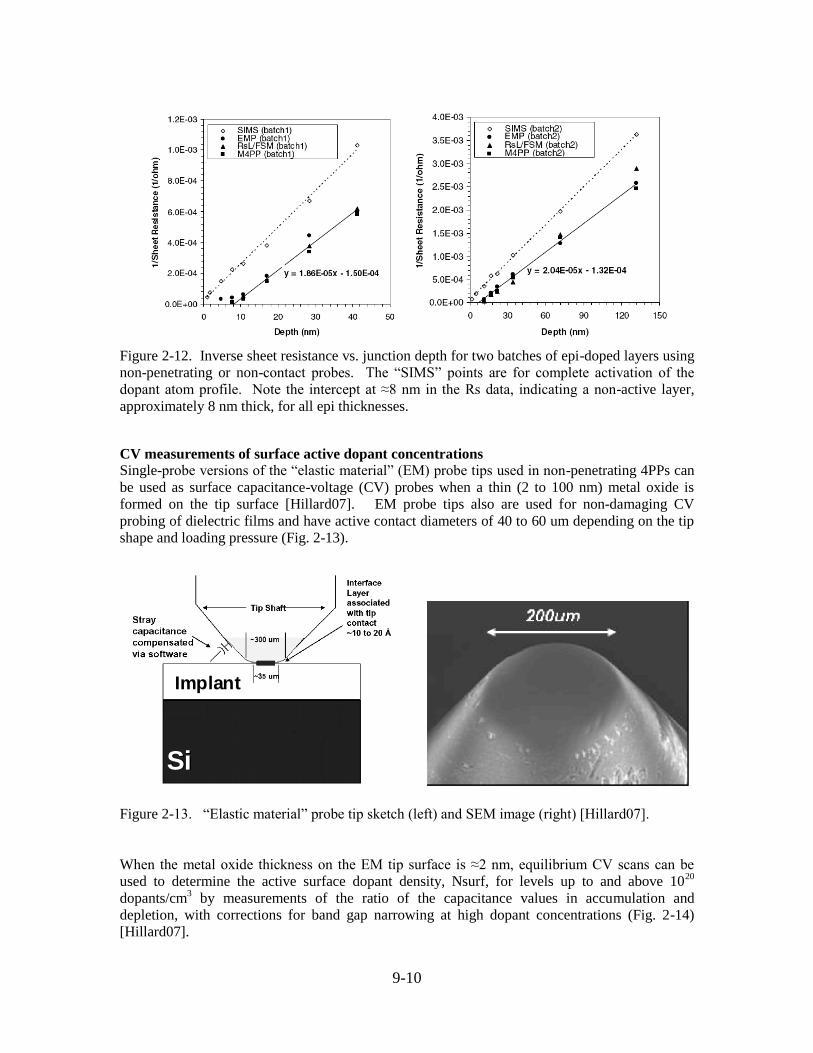
CV measurements of surface active dopant concentrations
Single-probe versions of the “elastic material” (EM) probe tips used in non-penetrating 4PPs can
be used as surface capacitance-voltage (CV) probes when a thin (2 to 100 nm) metal oxide is
formed on the tip surface [Hillard07]. EM probe tips also are used for non-damaging CV
probing of dielectric films and have active contact diameters of 40 to 60 um depending on the tip
shape and loading pressure (Fig. 2-13).
Figure 2-13. “Elastic material” probe tip sketch (left) and SEM image (right) [Hillard07].
When the metal oxide thickness on the EM tip surface is ≈2 nm, equilibrium CV scans can be
used to determine the active surface dopant density, Nsurf, for levels up to and above 1020
dopants/cm3 by measurements of the ratio of the capacitance values in accumulation and
depletion, with corrections for band gap narrowing at high dopant concentrations (Fig. 2-14)
[Hillard07].
Si
Implant
9-11
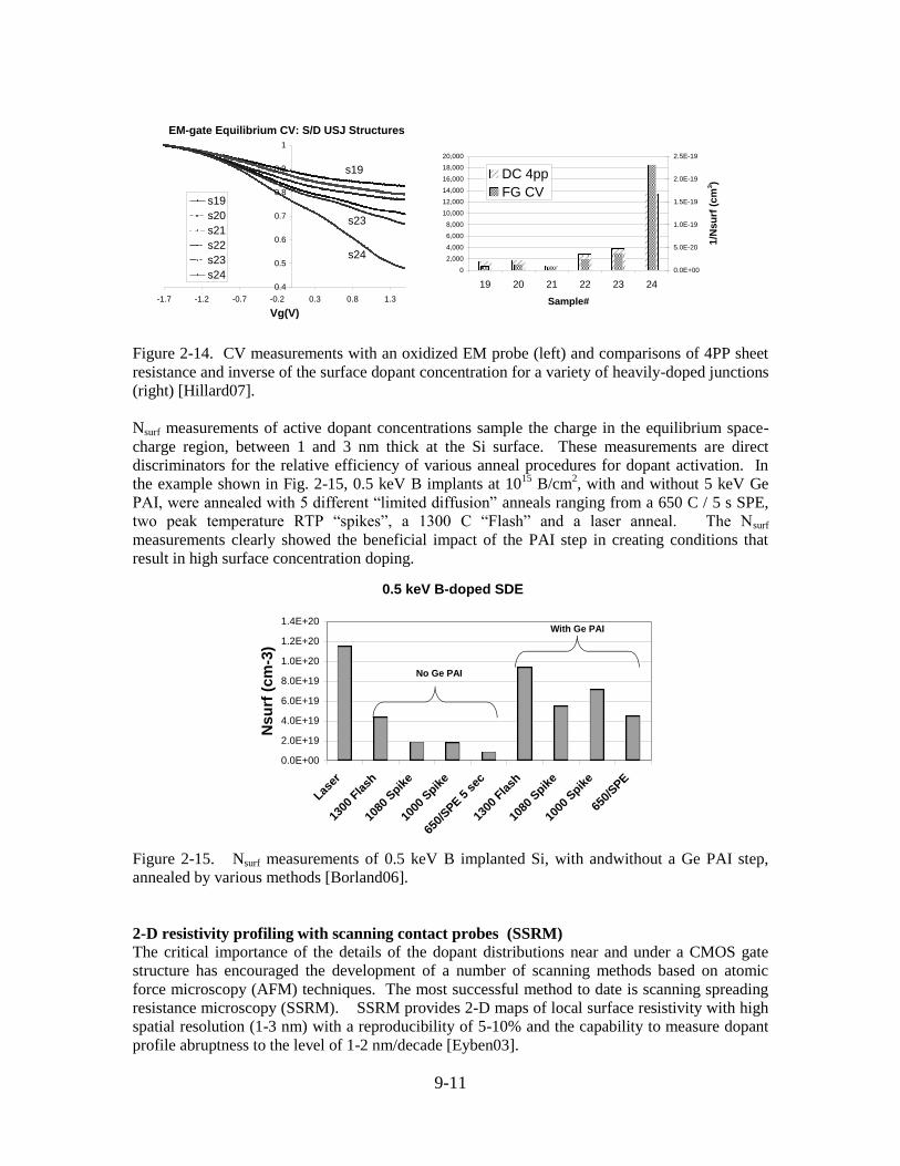
Figure 2-14. CV measurements with an oxidized EM probe (left) and comparisons of 4PP sheet
resistance and inverse of the surface dopant concentration for a variety of heavily-doped junctions
(right) [Hillard07].
Nsurf measurements of active dopant concentrations sample the charge in the equilibrium space-
charge region, between 1 and 3 nm thick at the Si surface. These measurements are direct
discriminators for the relative efficiency of various anneal procedures for dopant activation. In
the example shown in Fig. 2-15, 0.5 keV B implants at 1015
B/cm2, with and without 5 keV Ge
PAI, were annealed with 5 different “limited diffusion” anneals ranging from a 650 C / 5 s SPE,
two peak temperature RTP “spikes”, a 1300 C “Flash” and a laser anneal. The Nsurf
measurements clearly showed the beneficial impact of the PAI step in creating conditions that
result in high surface concentration doping.
Figure 2-15. Nsurf measurements of 0.5 keV B implanted Si, with andwithout a Ge PAI step,
annealed by various methods [Borland06].
2-D resistivity profiling with scanning contact probes (SSRM)
The critical importance of the details of the dopant distributions near and under a CMOS gate
structure has encouraged the development of a number of scanning methods based on atomic
force microscopy (AFM) techniques. The most successful method to date is scanning spreading
resistance microscopy (SSRM). SSRM provides 2-D maps of local surface resistivity with high
spatial resolution (1-3 nm) with a reproducibility of 5-10% and the capability to measure dopant
profile abruptness to the level of 1-2 nm/decade [Eyben03].
EM-gate Equilibrium CV: S/D USJ Structures
0.4
0.5
0.6
0.7
0.8
0.9
1
-1.7 -1.2 -0.7 -0.2 0.3 0.8 1.3
Vg(V)
C(p
F) s19
s20
s21
s22
s23
s24
s19
s24
s23
0.5 keV B-doped SDE
0.0E+00
2.0E+19
4.0E+19
6.0E+19
8.0E+19
1.0E+20
1.2E+20
1.4E+20
Laser
1300
Fla
sh
1080
Spik
e
1000
Spik
e
650/
SPE 5
sec
1300
Fla
sh
1080
Spik
e
1000
Spik
e
650/
SPE
Nsu
rf (
cm
-3)
No Ge PAI
With Ge PAI
0
2,000
4,000
6,000
8,000
10,000
12,000
14,000
16,000
18,000
20,000
19 20 21 22 23 24
Sample#
Rs (
Oh
ms
/sq
.)
0.0E+00
5.0E-20
1.0E-19
1.5E-19
2.0E-19
2.5E-19
1/N
su
rf (
cm
3)
DC 4pp
FG CV
9-12
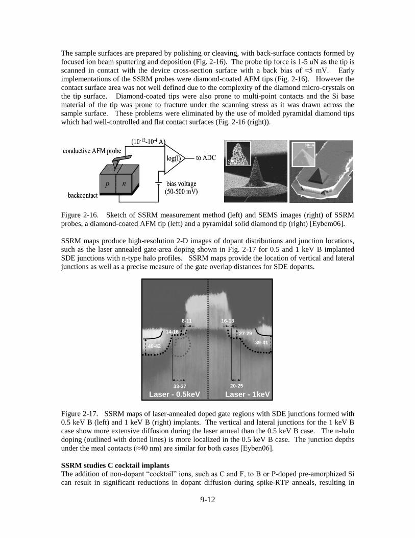
The sample surfaces are prepared by polishing or cleaving, with back-surface contacts formed by
focused ion beam sputtering and deposition (Fig. 2-16). The probe tip force is 1-5 uN as the tip is
scanned in contact with the device cross-section surface with a back bias of ≈5 mV. Early
implementations of the SSRM probes were diamond-coated AFM tips (Fig. 2-16). However the
contact surface area was not well defined due to the complexity of the diamond micro-crystals on
the tip surface. Diamond-coated tips were also prone to multi-point contacts and the Si base
material of the tip was prone to fracture under the scanning stress as it was drawn across the
sample surface. These problems were eliminated by the use of molded pyramidal diamond tips
which had well-controlled and flat contact surfaces (Fig. 2-16 (right)).
Figure 2-16. Sketch of SSRM measurement method (left) and SEMS images (right) of SSRM
probes, a diamond-coated AFM tip (left) and a pyramidal solid diamond tip (right) [Eybem06].
SSRM maps produce high-resolution 2-D images of dopant distributions and junction locations,
such as the laser annealed gate-area doping shown in Fig. 2-17 for 0.5 and 1 keV B implanted
SDE junctions with n-type halo profiles. SSRM maps provide the location of vertical and lateral
junctions as well as a precise measure of the gate overlap distances for SDE dopants.
14-16
16-18
33-37 20-25
39-4140-42
27-29
8-11
Laser - 0.5keV Laser - 1keV
14-16
16-18
33-37 20-25
39-4140-42
27-29
8-11
Laser - 0.5keV Laser - 1keV
14-16
16-18
33-37 20-25
39-4140-42
27-29
8-11
Laser - 0.5keV Laser - 1keV
14-16
16-18
33-37 20-25
39-4140-42
27-29
8-11
Laser - 0.5keV Laser - 1keV
Figure 2-17. SSRM maps of laser-annealed doped gate regions with SDE junctions formed with
0.5 keV B (left) and 1 keV B (right) implants. The vertical and lateral junctions for the 1 keV B
case show more extensive diffusion during the laser anneal than the 0.5 keV B case. The n-halo
doping (outlined with dotted lines) is more localized in the 0.5 keV B case. The junction depths
under the meal contacts (≈40 nm) are similar for both cases [Eyben06].
SSRM studies C cocktail implants
The addition of non-dopant “cocktail” ions, such as C and F, to B or P-doped pre-amorphized Si
can result in significant reductions in dopant diffusion during spike-RTP anneals, resulting in
9-13
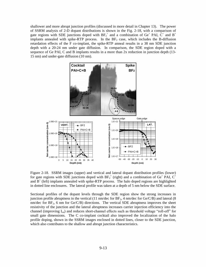
shallower and more abrupt junction profiles (discussed in more detail in Chapter 13). The power
of SSRM analysis of 2-D dopant distributions is shown in the Fig. 2-18, with a comparison of
gate regions with SDE junctions doped with BF2+ and a combination of Ge
+ PAI, C
+ and B
+
implants annealed with spike-RTP process. In the BF2 case, which includes the B-diffusion
retardation effects of the F co-implant, the spike-RTP anneal results in a 38 nm SDE junction
depth with a 20-24 nm under gate diffusion. In comparison, the SDE region doped with a
sequence of Ge PAI, C and B implants results in a more than 2x reduction in junction depth (13-
15 nm) and under-gate diffusion (10 nm).
Spike
BF2
Cocktail
PAI+C+B
9-11 20-24
4-6
32-36
60-62
92-96
37-3913-15
Spike
BF2
Cocktail
PAI+C+B
9-11 20-24
4-6
32-36
60-62
92-96
37-3913-15
1.00E+18
1.00E+19
1.00E+20
1.00E+21
0 5 10 15 20 25 30 35 40
Depth (nm)
Net
carr
ier
co
ncen
trati
on
(cm
-3)
BF2
PAI+C+B
VERT.
1.E+17
1.E+18
1.E+19
1.E+20
1.E+21
-50 -40 -30 -20 -10 0 10 20 30
Depth (nm)
Ne
t c
arr
ier
co
nc
en
tra
tio
n (
cm
-3)
BF2
PAI+C+B
LAT.
Gate edgeSpacer edge
Figure 2-18. SSRM images (upper) and vertical and lateral dopant distribution profiles (lower)
for gate regions with SDE junctions doped with BF2+ (right) and a combination of Ge
+ PAI, C
+
and B+ (left) implants annealed with spike-RTP process. The halo doped regions are highlighted
in dotted line enclosures. The lateral profile was taken at a depth of 5 nm below the SDE surface.
Sectional profiles of the dopant levels through the SDE region show the strong increases in
junction profile abruptness in the vertical (11 nm/dec for BF2, 4 nm/dec for Ge/C/B) and lateral (8
nm/dec for BF2, 6 nm for Ge/C/B) directions. The vertical SDE abruptness improves the sheet
resistivity of the junction and the lateral abruptness increases carrier injection efficiency into the
channel (improving Ion) and reduces short-channel effects such as threshold voltage “roll-off” for
small gate dimensions. The C co-implant cocktail also improved the localization of the halo
profile doping, shown in the SSRM images enclosed in dotted lines, closer to the SDE junction,
which also contributes to the shallow and abrupt junction characteristics.
9-14
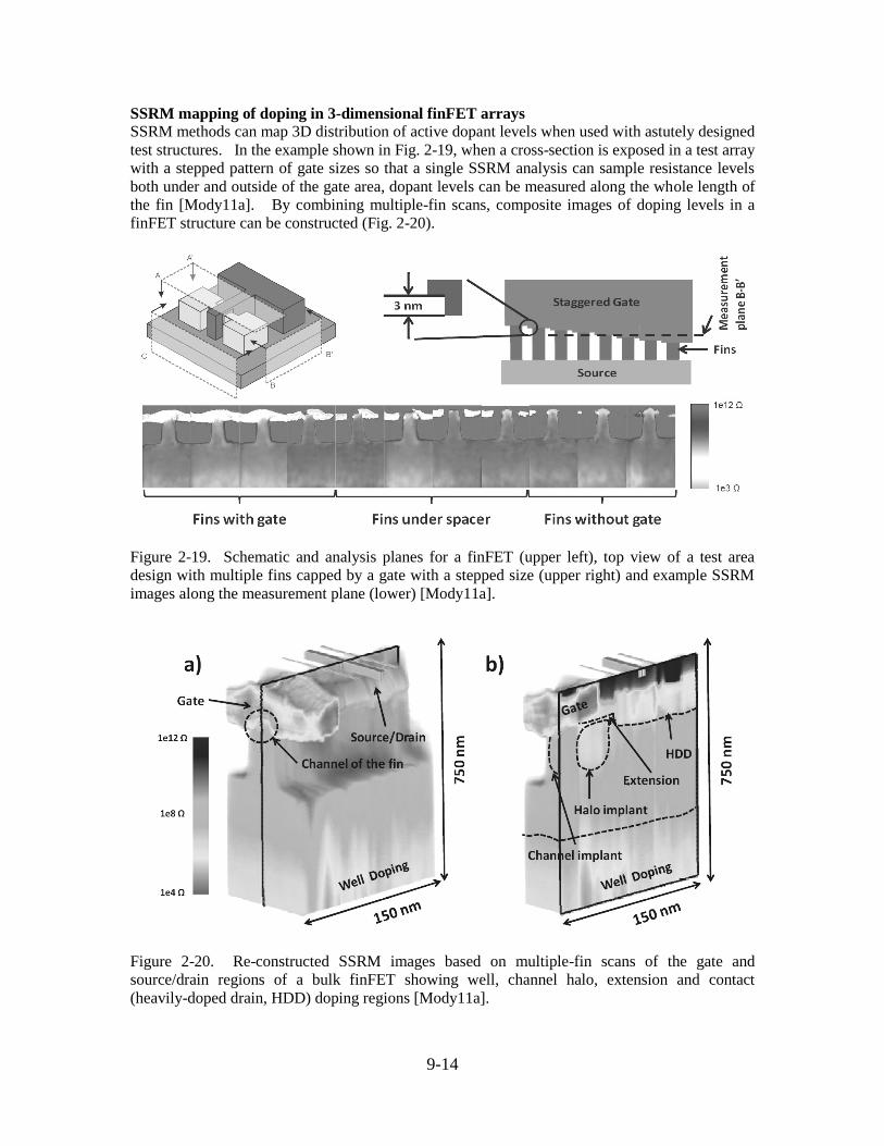
SSRM mapping of doping in 3-dimensional finFET arrays
SSRM methods can map 3D distribution of active dopant levels when used with astutely designed
test structures. In the example shown in Fig. 2-19, when a cross-section is exposed in a test array
with a stepped pattern of gate sizes so that a single SSRM analysis can sample resistance levels
both under and outside of the gate area, dopant levels can be measured along the whole length of
the fin [Mody11a]. By combining multiple-fin scans, composite images of doping levels in a
finFET structure can be constructed (Fig. 2-20).
Figure 2-19. Schematic and analysis planes for a finFET (upper left), top view of a test area
design with multiple fins capped by a gate with a stepped size (upper right) and example SSRM
images along the measurement plane (lower) [Mody11a].
Figure 2-20. Re-constructed SSRM images based on multiple-fin scans of the gate and
source/drain regions of a bulk finFET showing well, channel halo, extension and contact
(heavily-doped drain, HDD) doping regions [Mody11a].

9-15
3. Photo-voltage methods: The Surface Photo-Voltage (SPV) effect in semiconductors has been known for more than 50
years, [Brattain47, Brattain53]. In 1961 A. M. Goodman demonstrated that SPV dependence on
the intensity of irradiating light allows determination of minority carrier diffusion length in a
semiconductor, now widely used to monitor metal contamination in Si wafers [Goodman61]. The
basic grounds for the practical implementation of SPV metrology for dopants was developed by
R. Nakhmanson in a linear model of small signal ac-SPV [Nakhmanson75]. AC-SPV methods
were developed for measurement of doping density and resistivity of bulk semiconductors and
epi-layers [Kamieniecki97] and for analysis of ion implantation [Tsidilkovski04]. Analysis of
Junction Photo-Voltage (JPV) signals from light illuminated p-n junctions coupled with carrier
spreading and recombination effects gives a method for non-contact measurements of electrical
properties, junction sheet resistance and leakage current, known as RsL [Faifer94, Faifer04].
SPV basics The SPV effect is a change of a surface potential in a semiconductor resulting from illumination
of the surface with photons with energy greater than the Si bandgap. A surface potential in
semiconductor is due to a presence of different types of charges, such as fixed charge, trapped
and mobile charge, in a surface oxide layer and at the interface. Charge on the wafer surface
induces a space charge layer, with width W, in the semiconductor, that is a function of doping
concentration. Light can modify the surface potential by creating charge carriers in the bulk that
drift to the surface (Fig. 3-1). To establish a surface photo-voltage effect in semiconductor
materials, two components are needed: light with photon energy sufficient to generate electron-
hole pairs and an electric field, E. at the surface to separate those carrier pairs.
Figure 3-1. Schematic diagram of a Surface Photo Voltage (Vspv) measurement.
For small signal ac-SPV, where the modulated, super-band-gap light only slightly changes the
surface potential VSPV << kT, the photo-voltage response is proportional to the light intensity.
The signals yield either the space-charge capacitance (at high-frequencies) or minority carrier
lifetime (at low frequencies). The semiconductor resistivity can be determined from the space-
charge capacitance in inversion, and minority carrier lifetime can be used as an indicator of near-
surface metals contamination. Ion implantation introduces lattice defects, which act as recombination centers for charge carriers,
and changes the charge distribution in the implanted region. When light illuminates an implanted
sample, some of photo-generated carriers recombine at the defects before reaching the surface
(Fig. 3-2), reducing the measured photo-voltage. The higher the implant dose, the more
crystalline defects are created, the shorter is the photo-carrier lifetime and the smaller the surface
photo-voltage signal.
LIGHT SOURCE
Vspv
COUNTER ELECTRODE
Transparentelectrode
W - SurfaceDepletion Layer
-+
- - -+ + +
Beam of super band-gap light h > Eg
_
Semiconductor
+ + + + + + + + + +
+ + ++E
9-16
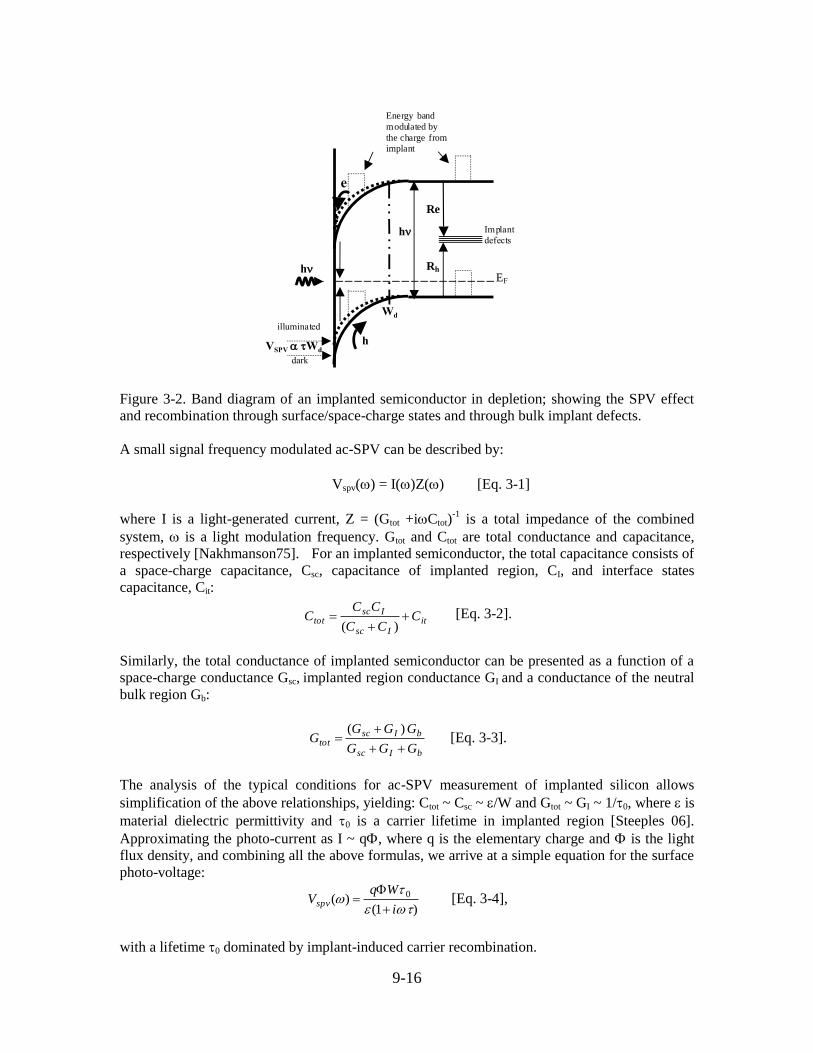
Figure 3-2. Band diagram of an implanted semiconductor in depletion; showing the SPV effect
and recombination through surface/space-charge states and through bulk implant defects.
A small signal frequency modulated ac-SPV can be described by:
Vspv() = I()Z() [Eq. 3-1]
where I is a light-generated current, Z = (Gtot +iCtot)-1
is a total impedance of the combined
system, is a light modulation frequency. Gtot and Ctot are total conductance and capacitance,
respectively [Nakhmanson75]. For an implanted semiconductor, the total capacitance consists of
a space-charge capacitance, Csc, capacitance of implanted region, CI, and interface states
capacitance, Cit:
itIsc
Isctot C
CC
CCC
)( [Eq. 3-2].
Similarly, the total conductance of implanted semiconductor can be presented as a function of a
space-charge conductance Gsc, implanted region conductance GI and a conductance of the neutral
bulk region Gb:
bIsc
bIsctot
GGG
GGGG
)( [Eq. 3-3].
The analysis of the typical conditions for ac-SPV measurement of implanted silicon allows
simplification of the above relationships, yielding: Ctot ~ Csc ~ /W and Gtot ~ GI ~ 1/0, where is
material dielectric permittivity and 0 is a carrier lifetime in implanted region [Steeples 06].
Approximating the photo-current as I ~ q, where q is the elementary charge and is the light
flux density, and combining all the above formulas, we arrive at a simple equation for the surface
photo-voltage:
)1()( 0
i
WqVspv
[Eq. 3-4],
with a lifetime 0 dominated by implant-induced carrier recombination.
h
h
VSPV Wd
illuminated
dark
h
Rh
Re
Wd
Energy band
modulated by
the charge from
implant
Implant
defects
EF
e
9-17
Another measured parameter, dynamic charge, Qd, makes correlation between photo-response
and material/implant parameters more lucid. Essentially, Qd is a function of Vspv and represents
the charge in a depletion layer modulated by the photo-carrier response:
Qd = kT/q(0W)2. [Eq. 3-5].
Calculating photo-carrier lifetime 0 allows correlation of dynamic charge Qd to the effective total
number of recombination centers induced by the implant process, Neff :
2
2
2
effi
id Nm
nqqnQ
[Eq. 3-6],
where Neff = (R)ND, is a charge carrier capture cross-section, R is an average width of an
implanted region and ND is a concentration of defects-recombination centers. Therefore, dynamic
charge, Qd , is proportional to the square of the implant-induced defect density and the width of
the implanted region.
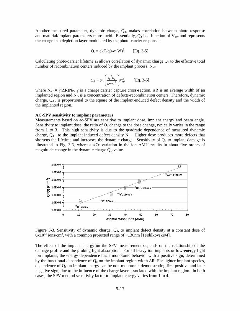
AC-SPV sensitivity to implant parameters
Measurements based on ac-SPV are sensitive to implant dose, implant energy and beam angle.
Sensitivity to implant dose, the ratio of Qd change to the dose change, typically varies in the range
from 1 to 3. This high sensitivity is due to the quadratic dependence of measured dynamic
charge, Qd , to the implant induced defect density ND. Higher dose produces more defects that
shortens the lifetime and increases the dynamic charge. Sensitivity of Qd to implant damage is
illustrated in Fig. 3-3, where a ≈7x variation in the ion AMU results in about five orders of
magnitude change in the dynamic charge QD value.
Figure 3-3. Sensitivity of dynamic charge, Qd, to implant defect density at a constant dose of
6x10¹³
ions/cm2, with a common projected range of ~130nm [Tsidilkovski04].
The effect of the implant energy on the SPV measurement depends on the relationship of the
damage profile and the probing light absorption. For all heavy ion implants or low-energy light
ion implants, the energy dependence has a monotonic behavior with a positive sign, determined
by the functional dependence of Qd on the implant region width R. For lighter implant species,
dependence of Qd on implant energy can be non-monotonic demonstrating first positive and later
negative sign, due to the influence of the charge layer associated with the implant region. In both
cases, the SPV method sensitivity factor to implant energy varies from 1 to 4.
1.0E+01
1.0E+02
1.0E+03
1.0E+04
1.0E+05
1.0E+06
1.0E+07
0 10 20 30 40 50 60 70 80
Atomic Mass Units (AMU)
Qd
(t)
(C/m
3)
31P
+, 92keV
40Ar
+, 116keV
49BF2
+, 156keV
75As
++, 211keV
11B
+, 35keV
9-18
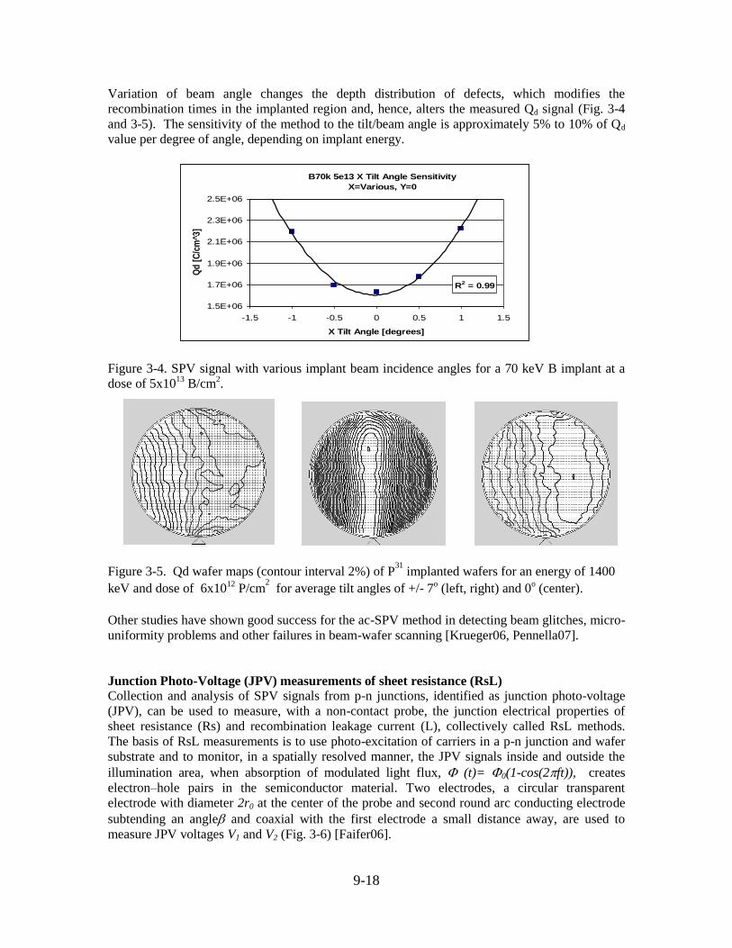
Variation of beam angle changes the depth distribution of defects, which modifies the
recombination times in the implanted region and, hence, alters the measured Qd signal (Fig. 3-4
and 3-5). The sensitivity of the method to the tilt/beam angle is approximately 5% to 10% of Qd
value per degree of angle, depending on implant energy.
Figure 3-4. SPV signal with various implant beam incidence angles for a 70 keV B implant at a
dose of 5x10¹³
B/cm2.
Figure 3-5. Qd wafer maps (contour interval 2%) of P31
implanted wafers for an energy of 1400
keV and dose of 6x10¹²
P/cm2 for average tilt angles of +/- 7
o (left, right) and 0
o (center).
Other studies have shown good success for the ac-SPV method in detecting beam glitches, micro-
uniformity problems and other failures in beam-wafer scanning [Krueger06, Pennella07].
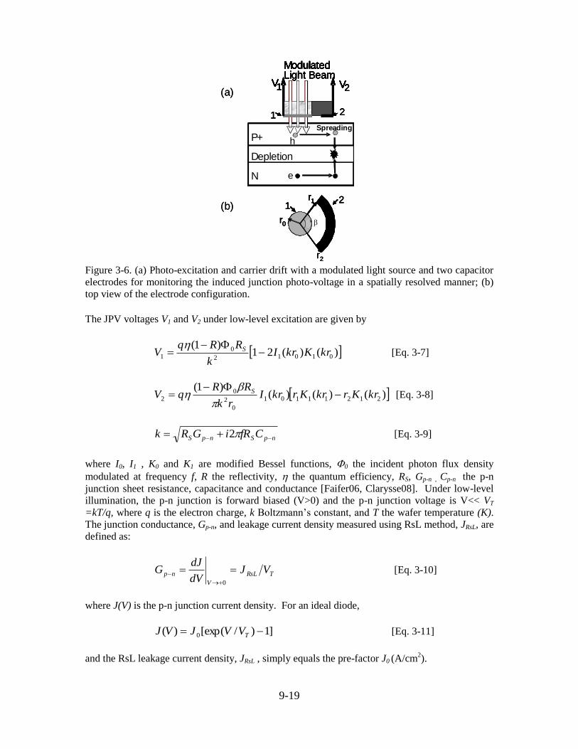
Junction Photo-Voltage (JPV) measurements of sheet resistance (RsL)
Collection and analysis of SPV signals from p-n junctions, identified as junction photo-voltage
(JPV), can be used to measure, with a non-contact probe, the junction electrical properties of
sheet resistance (Rs) and recombination leakage current (L), collectively called RsL methods.
The basis of RsL measurements is to use photo-excitation of carriers in a p-n junction and wafer
substrate and to monitor, in a spatially resolved manner, the JPV signals inside and outside the
illumination area, when absorption of modulated light flux, (t)= 0(1-cos(2ft)), creates
electron–hole pairs in the semiconductor material. Two electrodes, a circular transparent
electrode with diameter 2r0 at the center of the probe and second round arc conducting electrode
subtending an angle and coaxial with the first electrode a small distance away, are used to
measure JPV voltages V1 and V2 (Fig. 3-6) [Faifer06].
B70k 5e13 X Tilt Angle Sensitivity
X=Various, Y=0
R2 = 0.99
1.5E+06
1.7E+06
1.9E+06
2.1E+06
2.3E+06
2.5E+06
-1.5 -1 -0.5 0 0.5 1 1.5
X Tilt Angle [degrees]
Qd
[C
/cm
^3]
9-19
Figure 3-6. (a) Photo-excitation and carrier drift with a modulated light source and two capacitor
electrodes for monitoring the induced junction photo-voltage in a spatially resolved manner; (b)
top view of the electrode configuration.
The JPV voltages V1 and V2 under low-level excitation are given by
)()(21)1(
01012
01 krKkrI
k
RRqV S
[Eq. 3-7]
)()()()1(
21211101
0
2
0
2 krKrkrKrkrIrk
RRqV S
[Eq. 3-8]
npSnpS CfRiGRk 2 [Eq. 3-9]
where I0, I1 , K0 and K1 are modified Bessel functions, 0 the incident photon flux density
modulated at frequency f, R the reflectivity, the quantum efficiency, RS, Gp-n , Cp-n the p-n
junction sheet resistance, capacitance and conductance [Faifer06, Clarysse08]. Under low-level
illumination, the p-n junction is forward biased (V>0) and the p-n junction voltage is V<< VT
=kT/q, where q is the electron charge, k Boltzmann’s constant, and T the wafer temperature (K).
The junction conductance, Gp-n, and leakage current density measured using RsL method, JRsL, are
defined as:
TRsL
V
np VJdV
dJG
0
[Eq. 3-10]
where J(V) is the p-n junction current density. For an ideal diode,
]1)/[exp()( 0 TVVJVJ [Eq. 3-11]
and the RsL leakage current density, JRsL , simply equals the pre-factor J0 (A/cm2).
r2
Junction
Depletion
Substrate
Modulated Light Beam
V V2
P+
Depletion
N
Spreading
Modulated
V1 V
h
e
r0
r11
2
1 2
(a)
(b)
r2
Junction
Depletion
Substrate
Modulated Light Beam
V V2
P+
Depletion
N
Spreading
Modulated
V1 V
h
e
r0
r11
2
1 2
r2
Junction
Depletion
Substrate
Modulated Light Beam
V V2
P+
Depletion
N
Spreading
Modulated
V1 V
h
e
r0
r11
2
1 2
r2
Junction
Depletion
Substrate
Modulated Light Beam
V V2
P+
Depletion
N
Spreading
Modulated
V1 V
h
e
r0
r11
2
1 2
Junction
Depletion
Substrate
Modulated Light Beam
V V2
P+
Depletion
N
Spreading
Modulated
V1 V
h
e
r0
r11
2
1 2
(a)
(b)
9-20
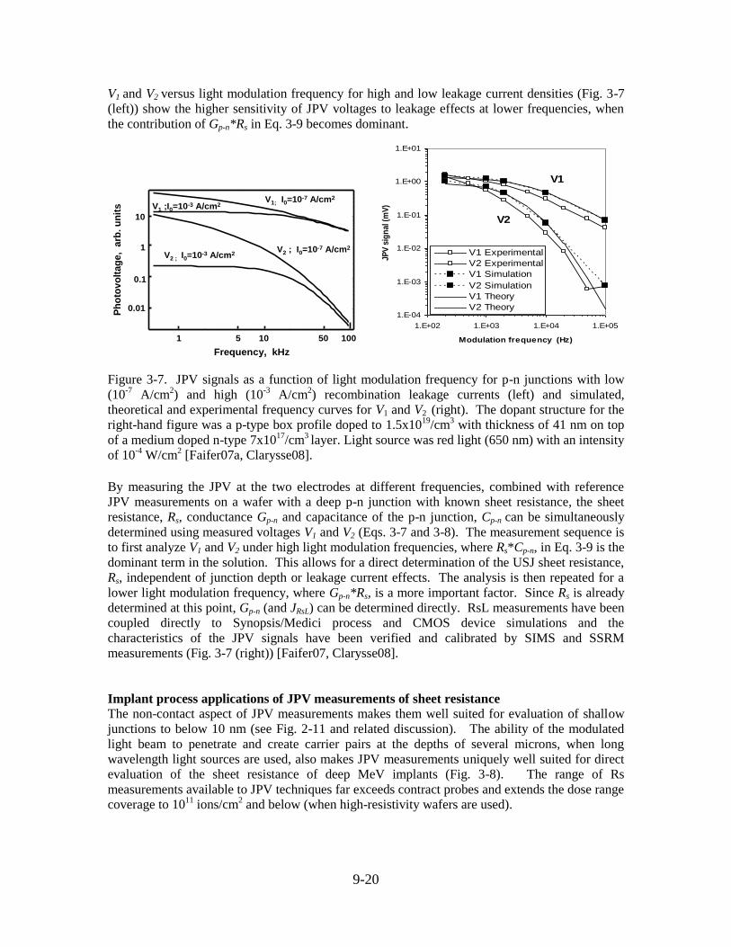
V1 and V2 versus light modulation frequency for high and low leakage current densities (Fig. 3-7
(left)) show the higher sensitivity of JPV voltages to leakage effects at lower frequencies, when
the contribution of Gp-n*Rs in Eq. 3-9 becomes dominant.
1 5 10 50 100
Frequency, kHz
0.01
0.1
1
10
V2 ; I0=10-3 A/cm2V2 ; I0=10-7 A/cm2
V1 ;I0=10-3 A/cm2V1; I0=10-7 A/cm2
Ph
oto
vo
lta
ge
, a
rb.
un
its
1 5 10 50 100
Frequency, kHz
0.01
0.1
1
10
V2 ; I0=10-3 A/cm2V2 ; I0=10-7 A/cm2
V1 ;I0=10-3 A/cm2V1; I0=10-7 A/cm2
Ph
oto
vo
lta
ge
, a
rb.
un
its
1.E-04
1.E-03
1.E-02
1.E-01
1.E+00
1.E+01
1.E+02 1.E+03 1.E+04 1.E+05
Modulation frequency (Hz)
JP
V s
ign
al (m
V)
V1 Experimental
V2 Experimental
V1 Simulation
V2 Simulation
V1 Theory
V2 Theory
V1
V2
Figure 3-7. JPV signals as a function of light modulation frequency for p-n junctions with low
(10-7
A/cm2) and high (10
-3 A/cm
2) recombination leakage currents (left) and simulated,
theoretical and experimental frequency curves for V1 and V2 (right). The dopant structure for the
right-hand figure was a p-type box profile doped to 1.5x10¹⁹
/cm3 with thickness of 41 nm on top
of a medium doped n-type 7x10¹⁷
/cm3 layer. Light source was red light (650 nm) with an intensity
of 10-4
W/cm2 [Faifer07a, Clarysse08].
By measuring the JPV at the two electrodes at different frequencies, combined with reference
JPV measurements on a wafer with a deep p-n junction with known sheet resistance, the sheet
resistance, Rs, conductance Gp-n and capacitance of the p-n junction, Cp-n can be simultaneously
determined using measured voltages V1 and V2 (Eqs. 3-7 and 3-8). The measurement sequence is
to first analyze V1 and V2 under high light modulation frequencies, where Rs*Cp-n, in Eq. 3-9 is the
dominant term in the solution. This allows for a direct determination of the USJ sheet resistance,
Rs, independent of junction depth or leakage current effects. The analysis is then repeated for a
lower light modulation frequency, where Gp-n*Rs, is a more important factor. Since Rs is already
determined at this point, Gp-n (and JRsL) can be determined directly. RsL measurements have been
coupled directly to Synopsis/Medici process and CMOS device simulations and the
characteristics of the JPV signals have been verified and calibrated by SIMS and SSRM
measurements (Fig. 3-7 (right)) [Faifer07, Clarysse08].
Implant process applications of JPV measurements of sheet resistance
The non-contact aspect of JPV measurements makes them well suited for evaluation of shallow
junctions to below 10 nm (see Fig. 2-11 and related discussion). The ability of the modulated
light beam to penetrate and create carrier pairs at the depths of several microns, when long
wavelength light sources are used, also makes JPV measurements uniquely well suited for direct
evaluation of the sheet resistance of deep MeV implants (Fig. 3-8). The range of Rs
measurements available to JPV techniques far exceeds contract probes and extends the dose range
coverage to 1011
ions/cm2 and below (when high-resistivity wafers are used).
9-21
Figure 3-8. Sheet resistance measurements with an RsL JPV probe ranging over 5 orders of
magnitude for dose and 2 orders of magnitude for energy. The energy range for JPV
measurements extends down to at least 0.2 keV for B ions.
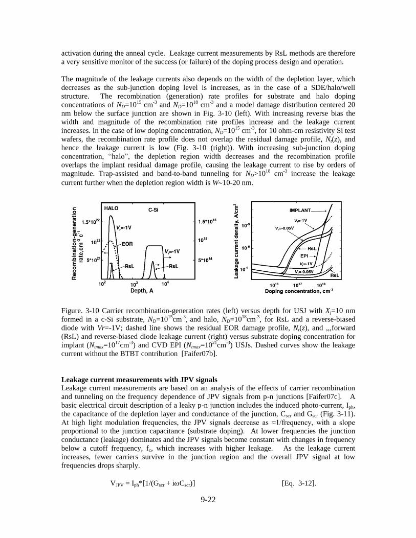
The speed of non-contact JPV measurements allows for continuous motion of the test junction
under the RsL probe and results in efficient collection of data for high-resolution (sub-mm2 pixel
size) Rs mapping (Fig. 3-9).
Figure 3-9. A high-resolution (30,000 pts/150 mmD, ≈0.6 mm2/pixel) Rs map of a 90 keV B
+,
4x10¹¹
B/cm2 implanted wafer with an x-y scanned ion beam. The average Rs is 57,671
Ohms/square with a uniformity of 2.4%
Leakage current measurements with RsL
Junctions are forward biased by ≈kT = 26 meV under low-intensity light illumination used for
JPV measurements. The current mechanisms in forward-bias include the diffusion current,
carrier recombination at the surface and at defects in the depletion layer and trap-assisted
tunneling to and from depletion layer defects. For reverse-bias junctions, such as in transistors
and diodes, the recombination mechanism is replaced by carrier generation at depletion layer
defects and band-to-band tunneling (BTBT) effects are added to the mix. Leakage currents in p-n
junctions and CMOS transistors are discussed in more detail in Chapter 13.
For heavily-doped shallow junctions, surface recombination rates are small so the relevant
forward bias leakage current effects are directly related to the size, number and location of defects
in the junction depletion layer, through carrier recombination and trap-assisted tunneling. The
nature and location of defects relative to the junction depends on the damage accumulation during
the various implantation steps and the recovery of the lattice structure and dopant diffusion and
9-22
activation during the anneal cycle. Leakage current measurements by RsL methods are therefore
a very sensitive monitor of the success (or failure) of the doping process design and operation.
The magnitude of the leakage currents also depends on the width of the depletion layer, which
decreases as the sub-junction doping level is increases, as in the case of a SDE/halo/well
structure. The recombination (generation) rate profiles for substrate and halo doping
concentrations of ND=1015
cm-3
and ND=1018
cm-3
and a model damage distribution centered 20
nm below the surface junction are shown in Fig. 3-10 (left). With increasing reverse bias the
width and magnitude of the recombination rate profiles increase and the leakage current
increases. In the case of low doping concentration, ND=1015
cm-3
, for 10 ohm-cm resistivity Si test
wafers, the recombination rate profile does not overlap the residual damage profile, Nt(z), and
hence the leakage current is low (Fig. 3-10 (right)). With increasing sub-junction doping
concentration, “halo”, the depletion region width decreases and the recombination profile
overlaps the implant residual damage profile, causing the leakage current to rise by orders of
magnitude. Trap-assisted and band-to-band tunneling for ND>1018
cm-3
increase the leakage
current further when the depletion region width is W10-20 nm.
Figure. 3-10 Carrier recombination-generation rates (left) versus depth for USJ with Xj=10 nm
formed in a c-Si substrate, ND=1015
cm-3
, and halo, ND=10
18cm
-3, for RsL and a reverse-biased
diode with Vr=-1V; dashed line shows the residual EOR damage profile, Nt(z), and ,,,forward
(RsL) and reverse-biased diode leakage current (right) versus substrate doping concentration for
implant (Ntmax=1017
cm-3
) and CVD EPI (Ntmax=1021
cm-3
) USJs. Dashed curves show the leakage
current without the BTBT contribution [Faifer07b].
Leakage current measurements with JPV signals
Leakage current measurements are based on an analysis of the effects of carrier recombination
and tunneling on the frequency dependence of JPV signals from p-n junctions [Faifer07c]. A
basic electrical circuit description of a leaky p-n junction includes the induced photo-current, Iph,
the capacitance of the depletion layer and conductance of the junction, Cscr and Gscr (Fig. 3-11).
At high light modulation frequencies, the JPV signals decrease as ≈1/frequency, with a slope
proportional to the junction capacitance (substrate doping). At lower frequencies the junction
conductance (leakage) dominates and the JPV signals become constant with changes in frequency
below a cutoff frequency, fc, which increases with higher leakage. As the leakage current
increases, fewer carriers survive in the junction region and the overall JPV signal at low
frequencies drops sharply.
VJPV = Iph*[1/(Gscr + iCscr)] [Eq. 3-12].

9-23
Figure 3-11. Circuit model (left) and frequency dependence of the JPV signals for a model
leaky p-n junction [Park01].
Measured JPV signals follow the general characteristics of the circuit model, with higher
frequency dependence slopes for heavier doped sub-junction regions (compare n-Si and n+(halo)
in Fig. 3-12) and the saturation and drop in JPV signals at low frequencies for increasingly leaky
junctions.
Figure 3-12. Measured JPV signals from shallow Boron-doped junctions in lightly-doped n-Si
test wafers and n-halo profiles annealed with RTP (low leakage) and laser (higher leakage)
anneals methods.
The measured RsL leakage, JRsL, is related to the junction conductance by (compare to Eq. 3-11):
JRsL = (q/kT)*Gscr = Jo(A/cm2) [Eq. 3-13].
The practical range of Jo measurements is ≈10-7
to ≈10-2
A/cm2.
CscrGscrIph
CscrGscrIph
.
fc
0.01
0.1
0.1 1 10
Gscr=10-4 Ohm-1*cm-2
Gscr=5*10-5
Gscr =10-5
JP
V,
arb
.un
it
.
fc
0.01
0.1
0.1 1 10
Gscr=10-4 Ohm-1*cm-2
Gscr=5*10-5
Gscr =10-5
Modulation frequency (Hz)
JP
V,
arb
.un
it
0.01
0.1
1
10
100
1000
100 1,000 10,000 100,000
Modulation Frequency (Hz)
Ju
ncti
on
Ph
oto
-vo
ltag
e, JP
Vo
ut
(mV
)
p+/n-Si
p+/n
+(halo)
leakage <10-7
A/cm2
leakage >10-3
A/cm2
RsL Data Analysis
9-24
Comparisons of Rs and leakage current maps based on JPV measurements is particularly
instructive for the case of limited-thermal budget annealing using flash lamp or laser methods.
For a “step-and-pulse” laser anneal, the shot-to-shot power variations in the laser anneal resulted
in local regions of the wafer with higher Rs and much higher leakage distributed over the wafer
(Fig. 3-13). The range of Rs values was ≈25% and the leakage current ranged over 2 orders of
magnitude.
Figure 3-13. 973-point Rs (left) and Jo (right) maps for a 0.5 keV B implant annealed with a
step-and-pulse laser on a 200 mm wafer. Regions of high Rs and Io are indicated with the darker
shading. Laser pulse-to-pulse power variations resulted in a global ≈25% variation in Rs around
an average of 996 Ohm/square and Io values from <10-7
to 2x10⁻⁵
A/cm2 [Current06].
4. Optical methods: Many types of optical probes have been used to characterize ion implanted surfaces. Modulated
optical reflectance, MOR, or “Therma-Wave”, has been widely used since the middle 80’s for
measurements of low-dose implants, with hundreds of tools in use. MOR is now employed to
track a wider range of implants, including shallow junctions. Recently, analysis of
photoluminescence (PL) signals arising from carrier recombination effects has been developed
for mapping of dose and anneal uniformity effects and for defect characterization with micron-
scale resolution images.
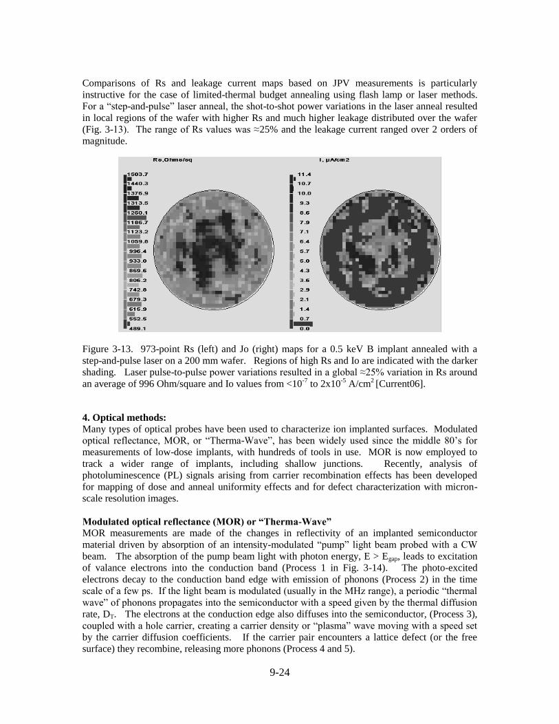
Modulated optical reflectance (MOR) or “Therma-Wave”
MOR measurements are made of the changes in reflectivity of an implanted semiconductor
material driven by absorption of an intensity-modulated “pump” light beam probed with a CW
beam. The absorption of the pump beam light with photon energy, E > Egap, leads to excitation
of valance electrons into the conduction band (Process 1 in Fig. 3-14). The photo-excited
electrons decay to the conduction band edge with emission of phonons (Process 2) in the time
scale of a few ps. If the light beam is modulated (usually in the MHz range), a periodic “thermal
wave” of phonons propagates into the semiconductor with a speed given by the thermal diffusion
rate, DT. The electrons at the conduction edge also diffuses into the semiconductor, (Process 3),
coupled with a hole carrier, creating a carrier density or “plasma” wave moving with a speed set
by the carrier diffusion coefficients. If the carrier pair encounters a lattice defect (or the free
surface) they recombine, releasing more phonons (Process 4 and 5).
9-25
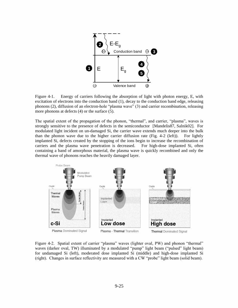
Figure 4-1. Energy of carriers following the absorption of light with photon energy, E, with
excitation of electrons into the conduction band (1), decay to the conduction band edge, releasing
phonons (2), diffusion of an electron-hole “plasma wave” (3) and carrier recombination, releasing
more phonons at defects (4) or the surface (5).
The spatial extent of the propagation of the phonon, “thermal”, and carrier, “plasma”, waves is
strongly sensitive to the presence of defects in the semiconductor [Mandelis87, Salnik02]. For
modulated light incident on un-damaged Si, the carrier wave extends much deeper into the bulk
than the phonon wave due to the higher carrier diffusion rate (Fig. 4-2 (left)). For lightly
implanted Si, defects created by the stopping of the ions begin to increase the recombination of
carriers and the plasma wave penetration is decreased. For high-dose implanted Si, often
containing a band of amorphous material, the plasma wave is quickly recombined and only the
thermal wave of phonons reaches the heavily damaged layer.
Figure 4-2. Spatial extent of carrier “plasma” waves (lighter oval, PW) and phonon “thermal”
waves (darker oval, TW) illuminated by a modulated “pump” light beam (“pulsed” light beam)
for undamaged Si (left), moderated dose implanted Si (middle) and high-dose implanted Si
(right). Changes in surface reflectivity are measured with a CW “probe” light beam (solid beam).
E Eg
E-Eg
Valence band
Conduction band
1
5
4
2
3
9-26
The reflectivity of the Si surface changes with the degree of accumulated damage as the dose
increases. At very low doses (<1010
ions/cm2) the MOR signal is dominated by the plasma wave
penetration into the bulk Si (Region I, Fig. 4-3). For higher doses, the dominant effect changes
from the carrier wave to the interaction of the phonon, “thermal”, wave with the accumulated
damage (Region II). For doses from ≈1011
to ≈1014
ions/cm2, the MOR signal rises with
increasing dose, dominated by the thermal wave effects (Region III). At doses where a buried
amorphous layer begins to grow, ≈1014
ions/cm2, and higher (Region IV), the MOR signal gets
more complex, with effects from optical interference effects by reflections from the surface and
amorphous regions as well as beam annealing by the pump beam.
Figure 4-3. MOR (“Therma-Wave”) signals as a function of dose for 100 keV As implanted Si
showing the amplitude and phase of the reflected signal (a) and close up of the low dose plasma
and thermal wave signals (b).
MOR measurements are made with co-linear (or nearly so) laser beams; a modulated Ar laser
“pump” beam and a CW He-Ne laser “probe” beam to monitor the reflectivity (4.4).
Figure 4-4. Block diagram of a MOR measurement, “Therma-probe”, system.
10
102
103
104
105
9 10 11 12 13 14 15 16
Log(Implantation dose),(ions/cm 2)
TW
am
plitu
de, a.u
.
-100
-80
-60
-40
-20
0
20
40
60
80
100
120
TW
ph
ase
, d
eg
ree
s
I II III IV
As-Si, 100 keV
10
102
103
104
9 10 11 12
TW
am
plitu
de, a.u
. PLASMA
THERMAL
TW SIGNAL
As-Si, 100 keV
Log(Implantation dose),(ions/cm 2)
9-27
MOR measurements are widely used for dose tracking of threshold implants in the range of 1011
to 1013
ions/cm2, as well as well, halo and SDE implants at higher doses. Because the pump and
probe beams, which are co-linear on the surface, can be focused to a spot of ≈1 um, MOR
techniques can be used to probe test pad areas on product wafers for in-line process controls.
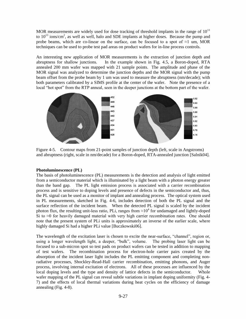
An interesting new application of MOR measurements is the extraction of junction depth and
abruptness for shallow junctions. In the example shown in Fig. 4.5, a Boron-doped, RTA
annealed 200 mm wafer was mapped with 21 sample points. The amplitude and phase of the
MOR signal was analyzed to determine the junction depths and the MOR signal with the pump
beam offset from the probe beam by 1 um was used to measure the abruptness (nm/decade); with
both parameters calibrated by a SIMS profile at the center of the wafer. Note the presence of a
local “hot spot” from the RTP anneal, seen in the deeper junctions at the bottom part of the wafer.
Figure 4-5. Contour maps from 21-point samples of junction depth (left, scale in Angstroms)
and abruptness (right, scale in nm/decade) for a Boron-doped, RTA-annealed junction [Salnik04].
Photoluminescence (PL)
The basis of photoluminescence (PL) measurements is the detection and analysis of light emitted
from a semiconductor material which is illuminated by a light beam with a photon energy greater
than the band gap. The PL light emission process is associated with a carrier recombination
process and is sensitive to doping levels and presence of defects in the semiconductor and, thus,
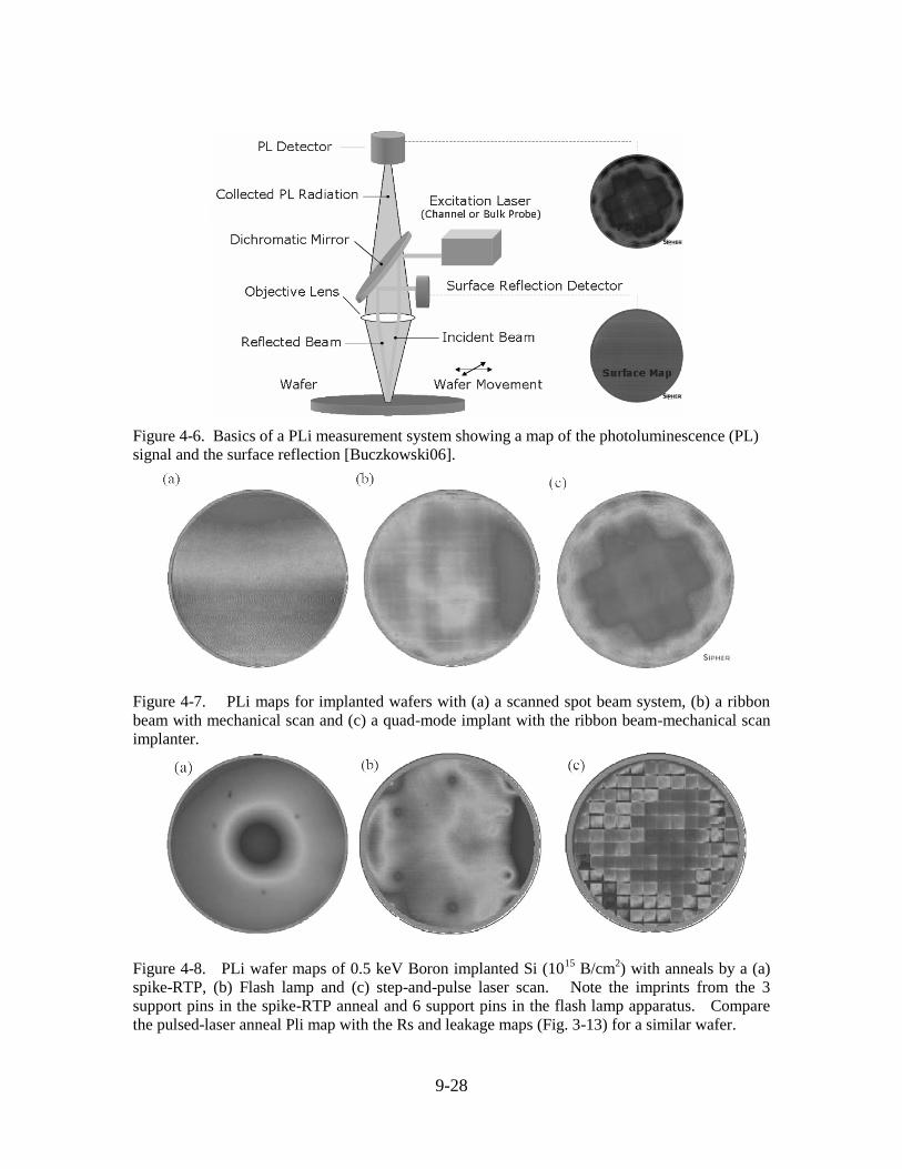
the PL signal can be used as a monitor of implant and annealing process. The optical system used
in PL measurements, sketched in Fig. 4-6, includes detection of both the PL signal and the
surface reflection of the incident beam. When the detected PL signal is scaled by the incident
photon flux, the resulting unit-less ratio, PLi, ranges from ≈104 for undamaged and lightly-doped
Si to ≈0 for heavily damaged material with very high carrier recombination rates. One should
note that the present system of PLi units is approximately an inverse of the earlier scale, where
highly damaged Si had a higher PLi value [Buczkowski06].
The wavelength of the excitation laser is chosen to excite the near-surface, “channel”, region or,
using a longer wavelength light, a deeper, “bulk”, volume. The probing laser light can be
focused to a sub-micron spot so test pads on product wafers can be tested in addition to mapping
of test wafers. The recombination process for electron-hole carrier pairs created by the
absorption of the incident laser light includes the PL emitting component and completing non-
radiative processes, Shockley-Read-Hall carrier recombination, emitting phonons, and Auger
process, involving internal excitation of electrons. All of these processes are influenced by the
local doping levels and the type and density of lattice defects in the semiconductor. Whole
wafer mapping of the PL signal can reveal subtle variations in implant doping uniformity (Fig. 4-
7) and the effects of local thermal variations during heat cycles on the efficiency of damage
annealing (Fig. 4-8).
9-28
Figure 4-6. Basics of a PLi measurement system showing a map of the photoluminescence (PL)
signal and the surface reflection [Buczkowski06].
Figure 4-7. PLi maps for implanted wafers with (a) a scanned spot beam system, (b) a ribbon
beam with mechanical scan and (c) a quad-mode implant with the ribbon beam-mechanical scan
implanter.
Figure 4-8. PLi wafer maps of 0.5 keV Boron implanted Si (10
15 B/cm
2) with anneals by a (a)
spike-RTP, (b) Flash lamp and (c) step-and-pulse laser scan. Note the imprints from the 3
support pins in the spike-RTP anneal and 6 support pins in the flash lamp apparatus. Compare
the pulsed-laser anneal Pli map with the Rs and leakage maps (Fig. 3-13) for a similar wafer.
9-29
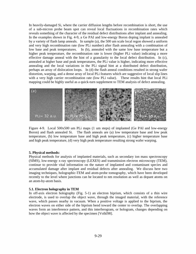
In heavily-damaged Si, where the carrier diffusion lengths before recombination is short, the use
of a sub-micron probe beam spot can reveal local fluctuations in recombination rates which
reveals something of the character of the residual defect distributions after implant and annealing.
In the examples shown in Fig. 4-9, a Ge PAI and low-energy Boron doping implant is annealed
by a variety of flash lamp anneals. In sample (a), the 500 um scale local regon showed a uniform
and very high recombination rate (low PLi number) after flash annealing with a combination of
low base and peak temperatures. In (b), annealed with the same low base temperature but a
higher peak temperature, the recombination rate is lower (higher PLi value) indicating a more
effective damage anneal with the hint of a granularity to the local defect distribution. In (c),
annealed at higher base and peak temperatures, the PLi value is higher, indicating more effective
annealing and the local variations in the PLi signal hint at a distributed defect distribution,
perhaps an array of dislocation loops. In (d) the flash anneal conditions resulted in strong wafer
distortion, warping, and a dense array of local PLi features which are suggestive of local slip lines
with a very high carrier recombination rate (low PLi value). These results hint that local PLi
mapping could be highly useful as a quick-turn supplement to TEM analysis of defect annealing.
Figure 4-9. Local 500x500 um PLi maps (1 um steps) of implanted (Ge PAI and low-energy
Boron) and flash annealed Si. The flash anneals are (a) low temperature base and low peak
temperature, (b) low temperature base and high peak temperature, (c) higher temperature base
and high peak temperature, (d) very high peak temperature resulting strong wafer warping.
5. Physical methods: Physical methods for analysis of implanted materials, such as secondary ion mass spectroscopy
(SIMS), low-energy x-ray spectroscopy (LEXES) and transmission electron microscopy (TEM),
continue to provide vital information on the nature of implanted and contaminant species and
accumulated damage after implant and residual defects after annealing. We discuss here two
imaging techniques, holographic-TEM and atom-probe tomography, which have been developed
recently to the level where junctions can be located to nm resolution as well as dopant atoms on
an atom-by-atom basis.
5.1. Electron holography in TEM
In off-axis electron holography (Fig. 5-1) an electron biprism, which consists of a thin wire
electrode, is used to overlap the object wave, through the imaged material, with the reference
wave, which passes nearby in vacuum. When a positive voltage is applied to the biprism, the
electron waves on either side of the biprism bend toward the center to overlap. The overlapping
waves form an interference pattern, and this interferogram, or hologram, changes depending on
how the object wave is affected by the specimen [Volkl98].
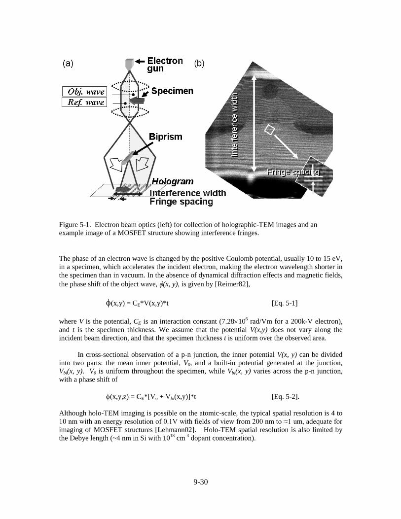
9-30
Figure 5-1. Electron beam optics (left) for collection of holographic-TEM images and an
example image of a MOSFET structure showing interference fringes.
The phase of an electron wave is changed by the positive Coulomb potential, usually 10 to 15 eV,
in a specimen, which accelerates the incident electron, making the electron wavelength shorter in
the specimen than in vacuum. In the absence of dynamical diffraction effects and magnetic fields,
the phase shift of the object wave, (x, y), is given by [Reimer82],
(x,y) = CE*V(x,y)*t [Eq. 5-1]
where V is the potential, CE is an interaction constant (7.28106 rad/Vm for a 200k-V electron),
and t is the specimen thickness. We assume that the potential V(x,y) does not vary along the
incident beam direction, and that the specimen thickness t is uniform over the observed area.
In cross-sectional observation of a p-n junction, the inner potential V(x, y) can be divided
into two parts: the mean inner potential, V0, and a built-in potential generated at the junction,
Vbi(x, y). V0 is uniform throughout the specimen, while Vbi(x, y) varies across the p-n junction,
with a phase shift of
(x,y,z) = CE*[Vo + Vbi(x,y)]*t [Eq. 5-2].
Although holo-TEM imaging is possible on the atomic-scale, the typical spatial resolution is 4 to
10 nm with an energy resolution of 0.1V with fields of view from 200 nm to ≈1 um, adequate for
imaging of MOSFET structures [Lehmann02]. Holo-TEM spatial resolution is also limited by
the Debye length (~4 nm in Si with 1018
cm-3
dopant concentration).
9-31
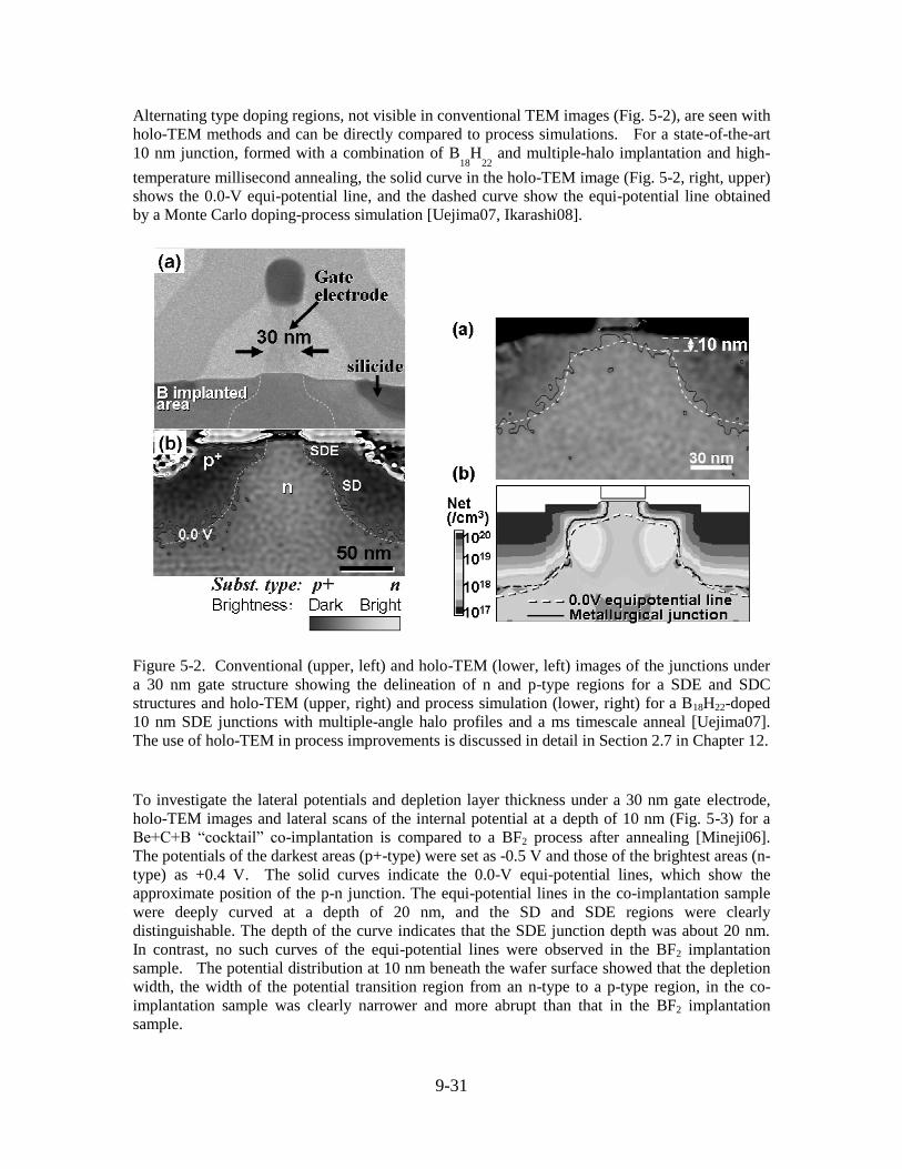
Alternating type doping regions, not visible in conventional TEM images (Fig. 5-2), are seen with
holo-TEM methods and can be directly compared to process simulations. For a state-of-the-art
10 nm junction, formed with a combination of B18
H22
and multiple-halo implantation and high-
temperature millisecond annealing, the solid curve in the holo-TEM image (Fig. 5-2, right, upper)
shows the 0.0-V equi-potential line, and the dashed curve show the equi-potential line obtained
by a Monte Carlo doping-process simulation [Uejima07, Ikarashi08].
Figure 5-2. Conventional (upper, left) and holo-TEM (lower, left) images of the junctions under
a 30 nm gate structure showing the delineation of n and p-type regions for a SDE and SDC
structures and holo-TEM (upper, right) and process simulation (lower, right) for a B18H22-doped
10 nm SDE junctions with multiple-angle halo profiles and a ms timescale anneal [Uejima07].
The use of holo-TEM in process improvements is discussed in detail in Section 2.7 in Chapter 12.
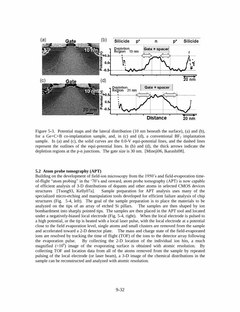
To investigate the lateral potentials and depletion layer thickness under a 30 nm gate electrode,
holo-TEM images and lateral scans of the internal potential at a depth of 10 nm (Fig. 5-3) for a
Be+C+B “cocktail” co-implantation is compared to a BF2 process after annealing [Mineji06].
The potentials of the darkest areas (p+-type) were set as -0.5 V and those of the brightest areas (n-
type) as +0.4 V. The solid curves indicate the 0.0-V equi-potential lines, which show the
approximate position of the p-n junction. The equi-potential lines in the co-implantation sample
were deeply curved at a depth of 20 nm, and the SD and SDE regions were clearly
distinguishable. The depth of the curve indicates that the SDE junction depth was about 20 nm.
In contrast, no such curves of the equi-potential lines were observed in the BF2 implantation
sample. The potential distribution at 10 nm beneath the wafer surface showed that the depletion
width, the width of the potential transition region from an n-type to a p-type region, in the co-
implantation sample was clearly narrower and more abrupt than that in the BF2 implantation
sample.
9-32
Figure 5-3. Potential maps and the lateral distribution (10 nm beneath the surface), (a) and (b),
for a Ge+C+B co-implantation sample, and, in (c) and (d), a conventional BF2 implantation
sample. In (a) and (c), the solid curves are the 0.0-V equi-potential lines, and the dashed lines
represent the outlines of the equi-potential lines. In (b) and (d), the thick arrows indicate the
depletion regions at the p-n junctions. The gate size is 30 nm. [Mineji06, Ikarashi08].
5.2 Atom probe tomography (APT)
Building on the development of field-ion microscopy from the 1950’s and field-evaporation time-
of-flight “atom probing” in the ‘70’s and onward, atom probe tomography (APT) is now capable
of efficient analysis of 3-D distributions of dopants and other atoms in selected CMOS devices
structures [Tsong93, Kelly07a]. Sample preparation for APT analysis uses many of the
specialized micro-etching and manipulation tools developed for efficient failure analysis of chip
structures (Fig. 5-4, left). The goal of the sample preparation is to place the materials to be
analyzed on the tips of an array of etched Si pillars. The samples are then shaped by ion
bombardment into sharply pointed tips. The samples are then placed in the APT tool and located
under a negatively-biased local electrode (Fig. 5-4, right). When the local electrode is pulsed to
a high potential, or the tip is heated with a local laser pulse, with the local electrode at a potential
close to the field evaporation level, single atoms and small clusters are removed from the sample
and accelerated toward a 2-D detector plate. The mass and charge state of the field-evaporated
ions are resolved by tracking the time of flight (TOF) of the ions to the detector array following
the evaporation pulse. By collecting the 2-D location of the individual ion hits, a much
magnified (≈106) image of the evaporating surface is obtained with atomic resolution. By
collecting TOF and location data from all of the atoms removed from the sample by repeated
pulsing of the local electrode (or laser beam), a 3-D image of the chemical distributions in the
sample can be reconstructed and analyzed with atomic resolution.
9-33
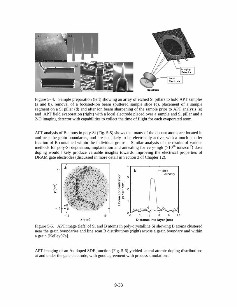
Figure 5- 4. Sample preparation (left) showing an array of etched Si pillars to hold APT samples
(a and b), removal of a focused-ion beam sputtered sample slice (c), placement of a sample
segment on a Si pillar (d) and after ion beam sharpening of the sample prior to APT analysis (e)
and APT field evaporation (right) with a local electrode placed over a sample and Si pillar and a
2-D imaging detector with capabilities to collect the time of flight for each evaporated atom.
APT analysis of B atoms in poly-Si (Fig. 5-5) shows that many of the dopant atoms are located in
and near the grain boundaries, and are not likely to be electrically active, with a much smaller
fraction of B contained within the individual grains. Similar analysis of the results of various
methods for poly-Si deposition, implantation and annealing for very-high (>1016
ions/cm2) dose
doping would likely produce valuable insights towards improving the electrical properties of
DRAM gate electrodes (discussed in more detail in Section 3 of Chapter 12).
Figure 5-5. APT image (left) of Si and B atoms in poly-crystalline Si showing B atoms clustered
near the grain boundaries and line scan B distributions (right) across a grain boundary and within
a grain [Kelley07a].
APT imaging of an As-doped SDE junction (Fig. 5-6) yielded lateral atomic doping distributions
at and under the gate electrode, with good agreement with process simulations.
9-34
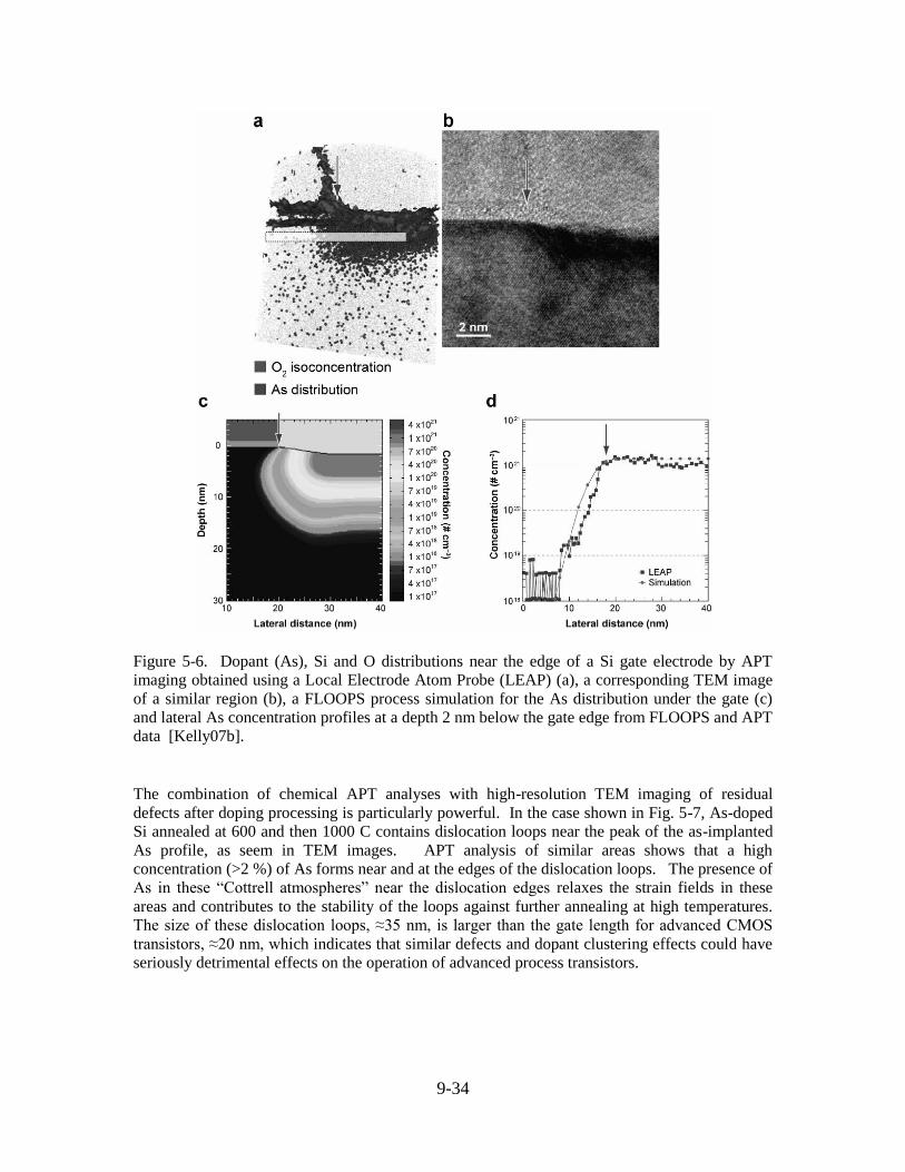
Figure 5-6. Dopant (As), Si and O distributions near the edge of a Si gate electrode by APT
imaging obtained using a Local Electrode Atom Probe (LEAP) (a), a corresponding TEM image
of a similar region (b), a FLOOPS process simulation for the As distribution under the gate (c)
and lateral As concentration profiles at a depth 2 nm below the gate edge from FLOOPS and APT
data [Kelly07b].
The combination of chemical APT analyses with high-resolution TEM imaging of residual
defects after doping processing is particularly powerful. In the case shown in Fig. 5-7, As-doped
Si annealed at 600 and then 1000 C contains dislocation loops near the peak of the as-implanted
As profile, as seem in TEM images. APT analysis of similar areas shows that a high
concentration (>2 %) of As forms near and at the edges of the dislocation loops. The presence of
As in these “Cottrell atmospheres” near the dislocation edges relaxes the strain fields in these
areas and contributes to the stability of the loops against further annealing at high temperatures.
The size of these dislocation loops, ≈35 nm, is larger than the gate length for advanced CMOS
transistors, ≈20 nm, which indicates that similar defects and dopant clustering effects could have
seriously detrimental effects on the operation of advanced process transistors.

9-35
Figure 5-7. TEM (left) and APT (right) images after As doping of Si and annealing at 600 C for
30 min and then 1000 C for 30 s. The APT image highlights As clustering, at concentrations
>2 %, at the edges of dislocation loops. A 2 nm native oxide film is seen in both images
[Thompson07].
APT analysis of doping in finFETs
APT provides atom-by-atom distributions of dopants and other atoms in 3D devices structures,
such as finFET channels. In the example shown in Fig. 5-8, the impact of beam incidence angle
on lateral B profiles in 40 nm thick finFET test structures is shown for sidewall incidence angles
of 10o and 45
o [Mody11b]. The APT data was collected after the implant anneal and contact
silicide formation, so the measured dopant distributions include the effect of implant and anneal
conditions.
Figure 5-8. Lateral and vertical profiles for B implants into ≈40 nm wide finFET test structures
with a grazing angle (10o) incidence on the fin sidewalls (left) and lateral profiles for SiO2, SiF
from fin sidewall oxides and B implants with a 45o beam incidence on the fin sidewall (right)
[Mody11b].
By comparing SSRM (see Fig. 2-19 and 2-20 and related text) and APT results (Fig. 5-9) one can
see that a large fraction of the B dopants near the finFET sidewalls were not electrically activated
(the sidewall atomic APT concentrations are much higher than the carrier concentrations from
SSRM analysis) by the process conditions used in this study.
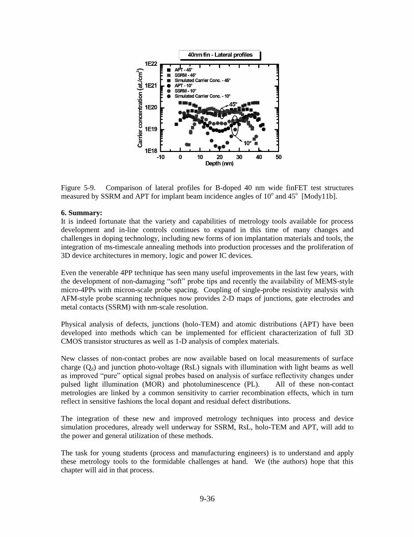
9-36
Figure 5-9. Comparison of lateral profiles for B-doped 40 nm wide finFET test structures
measured by SSRM and APT for implant beam incidence angles of 10o and 45
o [Mody11b].
6. Summary: It is indeed fortunate that the variety and capabilities of metrology tools available for process
development and in-line controls continues to expand in this time of many changes and
challenges in doping technology, including new forms of ion implantation materials and tools, the
integration of ms-timescale annealing methods into production processes and the proliferation of
3D device architectures in memory, logic and power IC devices.
Even the venerable 4PP technique has seen many useful improvements in the last few years, with
the development of non-damaging “soft” probe tips and recently the availability of MEMS-style
micro-4PPs with micron-scale probe spacing. Coupling of single-probe resistivity analysis with
AFM-style probe scanning techniques now provides 2-D maps of junctions, gate electrodes and
metal contacts (SSRM) with nm-scale resolution.
Physical analysis of defects, junctions (holo-TEM) and atomic distributions (APT) have been
developed into methods which can be implemented for efficient characterization of full 3D
CMOS transistor structures as well as 1-D analysis of complex materials.
New classes of non-contact probes are now available based on local measurements of surface
charge (Qd) and junction photo-voltage (RsL) signals with illumination with light beams as well
as improved “pure” optical signal probes based on analysis of surface reflectivity changes under
pulsed light illumination (MOR) and photoluminescence (PL). All of these non-contact
metrologies are linked by a common sensitivity to carrier recombination effects, which in turn
reflect in sensitive fashions the local dopant and residual defect distributions.
The integration of these new and improved metrology techniques into process and device
simulation procedures, already well underway for SSRM, RsL, holo-TEM and APT, will add to
the power and general utilization of these methods.
The task for young students (process and manufacturing engineers) is to understand and apply
these metrology tools to the formidable challenges at hand. We (the authors) hope that this
chapter will aid in that process.

9-37
Acknowledgements
The discussion of the specific metrologies this chapter was based on the work, advice and
publications of Pierre Eyben at IMEC, Peter Nielsen at CAPRES, Mark Benjamin at Solid State
Measurements, Edward Tsidilkovski at QC Solutions, Alex Salnik at KLA-Tencor, Andrzej
Buckowski at Nanometrics, Tom Kelly at Cameca/Imago, and Noboyuki Ikarashi at Renesas. In
addition, many co-workers contributed to the development, understanding and application of
these metrologies, including but certainly not limited to, Vladimir Faifer, Trudo Clarysse,
Wilfried Vandervorst, John Borland, Ken Steeples, Walt Johnson and Bob Hillard.
References Brattain 47 W.H. Brattain, Phys. Rev. 72 (1947), p.345
Brattain 53 W.H. Brattain, J. Bardeen, Bell System Tech. J. 32 (1953), p.1
Borland06 J. Borland, S. Shishiguchi, A. Mineji, W. Krull, D. Jacobson, M. Tanjyo, W. Lerch,
S. Paul, J. Gelpy, S. McCoy, J. Veturini, M.I. Current, V. Faifer, R. Hillard, M. Benjamin,
T. Walker,A. Buczkowski,Z.Li,J. Chen,“45nm node p+ USJ formation with high dopant
activation and low damage”, AIP Proc. 866 (2006) 96-100.
Buczkowski06 A. Buczkowski, Z. Li, T. Walker, S.G. Hummel, J.O. Borland, “Non-contact, image-based
photoluminescence metrology for ion implantation and annealing process inspection”,
AIP Proc. 866 (2006) 566-569.
Clarysse02 T. Clarysse, D. Vanhaeren, W. Vandervorst, “Impact of probe penetration on the electrical
characterization of sub-50 nm profiles”, J. Vac.Sc. Technol. B20 (1) (2002) 459-466.
Clarysse06 T. Clarysse, A. Moussa, F. Leys, R. Loo, W. Vandervorst, M.C. Benjamin, R.J. Hillard,
V.N. Faifer, M.I. Current, R. Lin, D.H. Petersen, “Accurate sheet resistance measurements
on ultra-shallow profiles”, Mat. Res. Soc . Proc. 912 (2006) 0912-C05-07.
Clarysse08 T. Clarysse, A. Moussa, T. Zangerle, F. Schaus, W. Vandervorst, V. Faifer, M. Current,
“Insights in junction photo-voltage based sheet resistance measurements for advanced
complementary metal-oxide semiconductor”, J. Vac. Sci. Technol. B26(1) (2008) 420-424.
Current06 M.I. Current, V.N. Faifer, T.M.H. Wong, T. Nguyen, A. Koo, “Non-contact sheet
resistance and leakage current monitoring of multi-implant ultra-shallow junctions:
doping and damage effects for ms-anneals” AIP Proc. 866 (2006) 582-585.
Current07 M. Current , V. Faifer, J. Halim, N. Ohno, “Dopant activation and leakage current
aspects of SDE/Halo CMOS junctions measured with non-contact junction photo-voltage
methods”, Proc 7th
Workshop on Junction Technology (2007) 43-46.
Eyben03 P. Eyben et al., AIP Conf. 638 (2003) 685.
Eyben06 P. Eyben, S. Severi, R. Duffy, B. Pawlak, E. Augendre, W. Vandervorst, “Analysis
and optimization of new implantation and activation mechanisms in ultra-shallow
junction implants using scanning spreading resistance microscopy (SSRM), Mat.
Res. Soc. Proc. 912 (2006) 0912-C05-08.
Faifer06 V.N. Faifer, M.I. Current, T.M.H. Wong, V.V. Souchkov, “Non-contact sheet
resistance and leakage current mapping for ultra-shallow junctions”, J. Vac.Sci. Technol.
B24(1) (2006) 414-420.
Faifer07a V.N. Faifer, M.I. Current, D.K. Schroder, “Characterization of ultrashallow junctions using
frequency-dependent junction photovoltage and its lateral attenuation”, App. Phys. Lett. 89
(2006) 151123.
Faifer07b V.N. Faifer, D.K. Schroder, M.I. Current, T. Clarysse, P.J. Timans, T. Zangerle,
W. Vandervorst, T.M.H. Wong, A. Moussa, S. McCoy, J. Gelpy, W. Lerch, S. Paul, D.
Bolze, J. Halim, “Influence of halo implant on leakage current and sheet resistance
of ultra-shallow p-n junctions”, J. Vac.Sci. Technol. B25 (2007) 1588-1592.
Faifer07c V.N. Faifer, M.I. Current, D.K. Schroder, T. Clarysse, W. Vandervorst, “Junction photo-
voltage (JPV) techniques for ultra-shallow junction characterization”, ECS Trans. 11(3)
(2007) 135-147.
Goodman61 A.M. Goodman, J. Appl. Phys. 32 (1961), p. 2550.
Hillard07 R.J. Hillard, C.Win Ye, J.O. Borland, “Dopant activation and profile determination
with an elastic material probe (EM-probe)”, AIP Proc. 931 (2007) 261- 264.

9-38
Ikarashi08 N. Ikarashi, M. Oshida, M. Miyamura, M. Saitoh, A. Mineji, S. Shishiguchi, M.Hane,
“Electron holography characterization of ultra-shallow junctions in 30 nm gate length
metal-oxide-semiconductor field-effect transistors”, Japan J. Appl. Phys. 74 (2008)
Kelly07a T.F. Kelly, D.J. Larson, K. Thompson, R.L. Alvis, J.H. Bunton, J.D. Olson, B.P. Gorman,
“Atom probe tomography of electronic materials” Annu. Rev. Mater. Res. 37 (2007)
681-727.
Kelly07b T.F. Kelly, J. Roberts, K. Thompson, “LEAP tomography of atomic materials”,
7th Workshop on Junction Technology (2007) 25-33.
Krueger06 C. Krueger, C.H. Ng, Z. Zhao, G. Krych, :”Surface charge profiling-an advancement in ion
implant monitoring”, AIP Conf. 866 (2006) 531-533.
Lehmann02 M. Lehmann, K. Brand, H. Lichte, Microscopy and Microanalysis, 8 (2002) 536.
Mandelis87 A. Mandelis, Ed., “Photoacoustic and Photothermal Phenomena in Semiconductors“,
(1987) North-Holland.
Mineji06 A. Mineji, S. Shishiguchi, “Ultra-shallow junction and super-steep halo formation using
carbon co-implantation for 65 nm high performance CMOS devices” 6th
Workshop on
Juncton Technology (2006) 84-87.
Mody11a J. Mody et al., “”3D-Carrier profiling in finFETs using Scanning Spreading Resistance
Microscopy”, IEDM11 (2011) 6.1.1-6.1.4.
Mody11b J. Mody et al., “Dopant and carrier profiling in finFET-based devices with sub-nanometer
resolution”, VLSI11 (2011).
Nakhmanson75 R.S. Nakhmanson, Solid State Electron. 18 (1975), p. 617
Pennella07 F. Pennelle, P. Pianezza, E. Tsidilkovski, G. Krych, K. Steeples, “Non-contact SPV-based
method for advanced ion implant process control”, Adv. Semi. Manu. Conf (2007).
Park01 G.E.Park, D.K. Schroder,et al., J. Electrochem.Soc.148, (2001) G411.
Perloff76 D.S. Perloff, J. Electrochem. Soc. 123 (1976) 1745.
Petersen03 C.I. Petersen, D. Worledge, P.R. Petersen, “Reproducibility of nano-and micro-scale multi-
point probe sheet resistance measurements”, Mat. Res. Soc. Proc. 738 (2003) G4.3.1.
Petersen06 C. Petersen, R. Lin, D.H. Petersen, P.F. Nielsen, “Micro-scale sheet resistance
measurements on ultra-shallow junctions” RTP06 (2006).
Petersen08 D.H. Petersen, R. Lin, T.M. Hansen, E. Rosseel, W. Vandervorst, C. Markvardsen,
D. Kjaer, P.F. Nielsen, “Comparative study of size dependent four-point probe
sheet resistance measurements on laser annealed ultra-shallow junctions”,
J. Vac. Sci. Technol. B26(1) 362-367.
Reimer82 L. Reimer, “Transmission Electron Microscopy”, Springer-Verlag, (1982).
Salnik02 A. Salnik and J. Opsal, “Quantitative photo-thermal characterization of ion-
implanted layers in Si”, J. Appl. Phys. 91, 2874 (2002).
Salnik03 A. Salnik and J. Opsal, “Dynamics of the plasma and thermal waves in surface-
modified semiconductors”, Rev. Sci. Instrum. 74, 545 (2003)
Salnik04 A. Salnik, L. Nicolaidesw, J. Opsal, A. Jain, D. Rogers, L. Robertson, “Simultaneous
determination of ultra-shallow juctions depth and abruptness using thermal wave
technique”, Rev. Sci Instrum. 75(6) (2004) 2144-2148.
Steeples 06 K. Steeples, E. Tsidilkovski, “Photoelectric Measurement Method For Implanted Silicon:
A Phenomenological Approach”, Ion Implant Technology, AIP CP866 (2006), 558-561.
Thomson07 K. Thompson, P.L. Flaitz, P. Ronsheim, D.J. Larson, T.F. Kelly, “Imaging of
Arsenic Cottrell atmospheres around Silicon defects by three-dimensional atom
probe tomography”, Science 317 (2007) 1370-1373.
Tsidilkovski04 E. Tsidilkovski, K. Crocker. K. Steeples, “Ion implant process monitoring with a dynamic
surface photo-charge technique”, Adv. Semi. Manu. Conf. (2004).
Tsong93 T.T. Tsong, “Atom-probe field ion microscopy” PhysicsToday, May 1993, 24-31.
Uejima07 K. Uejima, K. Yako, N. Ikarashi, M. Tanaka, T. Nagumo, A. Mineji,
S. Shishiguchi, M. Hane, “Pushing planar bulk CMOSFET scaling to its limit by
ultimately shallow diffusion-less junctions”, IEDM07 (2007) 151-154.
Van der Pauw58 L.J. van der Pauw, Philips Res. Rep. 13 (1958) 1.
Volkl98 E. Völkl, L.F. Allard and D.C. Joy, Ed., “Introduction to Electron Holography”, Plenum,
New York (1998).
Related Documents