ORDER NO. CPD0604068C1 Notebook Computer CF-29 Model No. CF-29XXXXXXM This is the Service Manual for the following areas. M …for U.S.A. and Canada © 2006 Matsushita Electric Industrial Co., Ltd. All rights reserved. Unauthorized copying and distribution is a violation of law.

CF 29 Service Manual
Oct 24, 2015
CF 29 Notebook Computer Service Manual
Welcome message from author
This document is posted to help you gain knowledge. Please leave a comment to let me know what you think about it! Share it to your friends and learn new things together.
Transcript

ORDER NO. CPD0604068C1
Notebook Computer
CF-29
Model No. CF-29XXXXXXM
This is the Service Manual for the following areas. M …for U.S.A. and Canada
© 2006 Matsushita Electric Industrial Co., Ltd. All rights reserved.Unauthorized copying and distribution is a violation of law.

This apparatus must be earthed for your safety.To ensure safe operation the three-pin plug must be inserted only into a standard three-pin power pointwhich is effectively earthed through the normal household wiring.Extension cords used with the equipment must be three-core and be correctly wired to provide connec-tion to earth. Wrongly wired extension cords are a major cause of fatalities.The fact that the equipment operates satisfactorily does not imply that the power point is earthed andthat the installation is completely safe.For your safety, if you have any doubt about the effective earthing of the power point, consult a quali-fied electrician.FOR YOUR SAFETY PLEASE READ THE FOLLOWING TEXT CAREFULLYThis appliance is supplied with a moulded three pin mains plug for your safety and convenience.A 3 amp fuse is fitted in this plug.Should the fuse need to be replaced please ensure that the replacement fuse has a rating of 3 amps andthat it is approved by ASTA or BSI to BS 1362.
Check for the ASTA mark or the BSI mark on the body of the fuse.If the plug contains a removable fuse cover you must ensure that it is refitted when the fuse is replaced.If you lose the fuse cover the plug must not be used until a replacement cover is obtained.A replacement fuse cover can be purchased from your local Panasonic Dealer.IF THE FITTED MOULDED PLUG IS UNSUITABLE FOR THE SOCKET OUTLET IN YOURHOME THEN THE FUSE SHOULD BE REMOVED AND THE PLUG CUT OFF AND DISPOSEDOF SAFELY.THERE IS A DANGER OF SEVERE ELECTRICAL SHOCK IF THE CUT OFF PLUG IS INSERTEDINTO ANY 13 AMP SOCKET.If a new plug is to be fitted please observe the wiring code as shown below.If in any doubt please consult a qualified electrician.Warning: THIS APPLIANCE MUST BE EARTHED.ImportantThe wires in this mains lead are coloured in accordance with the following code:Green-and-yellow: EarthBlue: NeutralBrown: LiveAs the colours of the wires in the mains lead of this apparatus may not correspond with the colouredmarkings identifying the terminals in your plug, proceed as follows:The wire which is coloured GREEN-and-YELLOW must be connected to the terminal in the plugwhich is marked by the letter E or by the safety earth symbol coloured GREEN or GREEN-and-YELLOW.
The wire which is coloured Blue must be connected to the terminal which is marked with the letter N orcoloured BLACK.The wire which is coloured Brown must be connected to the terminal which is marked with the letter Lor coloured RED.
The mains plug on this equipment must be used to disconnect the mains power.Please ensure that a socket outlet is available near the equipment and shall be easily accessible.
How to replace the fuseOpen the fuse compartment with a screw-driver and replace the fuse.
WarningsThis equipment is not designed for connection to an IT power system.(An IT system is a system having no direct connections between live parts and Earth; the exposed-conducive-parts of the electrical installation are earthed.An IT system is not permitted where the computer is directly connected to public supply systems in the U.K.)
Disconnect the mains plug from the supply socket when the computer is not in use.
This equipment is produced to BS800/1983.
For U.K.
WARNING
1

2
LASER SAFETY INFORMATIONFor U.S.A.
Class 1 LASER-ProductThis product is certified to comply with DHHS Rules 21 CFR Subchapter J.This product complies with European Standard EN60825 (or IEC Publication 825)
For all areasThis equipment is classified as a class 1 level LASER product and there is no hazardous LASER radiation.
Caution:(1) Use of controls or adjustments or performance of procedures other than those specified herein may result in
hazardous radiation exposure.(2) The drive is designed to be incorporated into a computer-based system or unit which has an enclosing cover.
It should never be used as a stand alone drive.
Danger:The serviceman should not remove the cover of drive unit and should not service because the drive unit is a non-serviceable part.Please check DANGER label on PD-drive unit.
• Unplug the AC power cord to the equipment before opening the top cover of the drive.When the power switch it on, do not place your eyes close to the front panel door to look into the interior of the unit.
LASER SpecificationClass 1 level LASER ProductWave Length: DVD 658±8 nm
CD 775~815 nm
Laser safety information is appropriate only when drive with laser is installed.

3

4

CONTENTS 1 Diagnosis Procedure ······································································································1-1
2 Power-On Self Test (Boot Check) ··················································································2-1
3 List of Error Codes ··········································································································3-1
4 Diagnostic Test ···············································································································4-1
5 Self Diagnosis Test ·········································································································5-1
6 Wiring Connection Diagram ···························································································6-1
7 Disassembly/Reassembly ······························································································7-1
8 Exploded View ················································································································8-1
9 Replacement Parts List ··································································································9-1

1-1
1 Diagnosis Procedure1.1. Basic Procedure

1-2
Please take note of the following two points with regard to troubleshooting: 1. Know-how of diagnosis upon occurrence of heavy troubles, e.g. ‘Set cannot be turned ON’, ‘Set fails to start’, ‘No display on
screen’, etc. 2. Explanation of each trouble, mainly symptom of trouble in operation.
Flow Chart
NG
NO
YES
NO
YES
NG
NO
YESNG
OK
OK
NO
YES
NG
OK
NG
OK
NO
YES
OK
OK
NG
START START Pay attention to the following points when in pursuit of the cause of a troubleshooting. 1. Peripheral apparatus connected with the set should all be removed before operation check. 2. Make sure that cables, boards, etc. are not coming off, and recheck the contact condition.
Set cannot be supplied with current. Power lamp fails to light up.
AC Adaptor/Battery Output voltage
Replace AC Adaptor/Battery
Return set-up utility setpoint to the state of ‘delivery from factory’.
Make sure of contact of K/B connector in use.Replace keyboard or main board.
Replace DVD drive. Replace main board.
Reinstall HDD. Replace main board.
Power lamp check
Check contact condition of power input terminal. Replace ifdefective. Check Power SW. Replace if defective.
Inverter board Replace inverter board. Check inverter cable continuity. Replace if defective
Replace LCD back light.
BIOS operation check
Replace main board (Check fuse at power source).
LCD unit check
Replace LCD unit.
Result of POST
Refer to POST error code table.
Replace main board.
Main board check
Replace main board
HDD access
Check HDD cable connection and continuity. Replace if defective. Replace HDD & Reinstall. Replace main board.
Set-up utility starting Replace main board.
Troublesymptoms on some
of DVD or CD
Check if there are any flaws on DVD or CDmedia. Since flaws may appear on specificmedia, DVD or CD media can be defective.
START END
Dark display on screen. Screen fails to display.
Failure in starting
Not displayed properly on screen.
Some or all keys cannot be input.
DVD/CD CALL not practicable.
Starts but operates unstably.
Heavy trouble e.g., ‘Set cannot be turned ON’, ‘Set fails to start’, ‘No display on screen’, etc.
Each kind of trouble in operation.
*Clean DVD-ROM drive with an applicator.
LCD back light lighting
1.2. Troubleshooting

2-1
2 Power-On Self Test (Boot Check) Outline of POST
The set has a boot check function called POST (Power-On Self Test) in it. The condition of the main body is diagnosed by checkingbeep sound or error code.
Start .............Test begins automatically when power switch is set to ON. Normal finish .....After memory checking, a beep sound is issued once and the set is placed into automatic stop.
Note: If no error occurs, nothing is displayed. (No display of OK, etc.)
Error Diagnosis by Checking Beep Signal SoundThe beep sound is as follows:
= long sound (about 0.4 sec.), = short sound (about 0.2 sec.), Length between sounds is about 0.1 sec.
Table of errors classified by beep sounds
(1 (long sound) -2-3-4)
(Length of bar shows length of sound.)
Diagnosis Beep signal sound Error message1(long sound)-2 BIOS ROM error
BIOS ROM errorRAM errorKeyboard controller errorRAM errorRAM errorRAM error
1-2-2-31-3-1-11-3-1-31-3-4-11-3-4-31-4-1-1
BIOS ROM error2-1-2-3Occurrence of unexpected offering2-2-3-1
Main board
(Note) A beep sound is also issued in case of other I/O trouble.

3-1
3. List of Error Codes <Only when the port replicator is connected> The following is a list of the messages that BIOS can display. Most of them occur during POST. Some of them display information about a hardware device, e.g., the amount of memory installed. Others may indicate a problem with a device, such as the way it has been configured. Following the list are explanations of the messages and remedies for reported problems. If your system displays one of except the messages marked below with an asterisk (*), write down the message and contact Panasonic Technical Support. If your system fails after you make changes in the Setup menus, reset the computer, enter Setup and install Setup defaults or correct the error.
0200 Failure Fixed Disk Fixed disk in not working or not configured properly. Check to see if fixed disk is attached properly. Run Setup. Find out if the fixed-disk type is correctly identified.
0210 Stuck key Stuck key on keyboard.
0211 Keyboard error Keyboard not working.
0212 Keyboard Controller Failed Keyboard controller failed test. May require replacing keyboard controller.
0213 Keyboard locked - Unlock key switch Unlock the system to proceed.
0230 System RAM Failed at offset: nnnn System RAM failed at offset nnnn of in the 64k block at which the error was detected.
0231 Shadow RAM Failed at offset: nnnn Shadow RAM failed at offset nnnn of the 64k block at which the error was detected.
0232 Extended RAM Failed at offset: nnnn Extended memory not working or not configured properly at offset nnnn.
0250 System battery is dead - Replace and run SETUP The CMOS clock battery indicator shows the battery is dead. Replace the battery and run Setup to reconfigure the system.
*0251 System CMOS checksum bad - Default configuration used System CMOS has been corrupted or modified incorrectly, perhaps by an application program that changes data stored in CMOS. The BIOS installed Default SETUP Values. If you do not want these values, enter Setup and enter your own values. If the error persists, check the system battery or contact Panasonic Technical Support.
0260 System timer error The timer test failed. Requires repair of system board.
0270 Real time clock error Real-time clock fails BIOS test. May require board repair.
*0280 Previous boot incomplete - Default configuration used Previous POST did not complete successfully. POST loads default values and offers to run Setup. If the failure was caused by incorrect values and they are not corrected, the next boot will likely fail. On systems with control of wait states, improper Setup settings can also terminate POST and cause this error on the next boot. Run Setup and verify that the wait-state configuration is correct. This error is cleared the next time the system is booted.
0281 Memory Size found by POST differed from EISA CMOS Memory size found by POST differed from EISA CMOS.

3-2
02D0 System cache error - Cache disabled Contact Panasonic Technical Support.
02F0: CPU ID: CPU socket number for Multi-Processor error.
02F4: EISA CMOS not writable ServerBIOS2 test error: Cannot write to EISA CMOS.
02F5: DMA Test Failed ServerBIOS2 test error: Cannot write to extended DMA (Direct Memory Access) registers.
02F6: Software NMI Failed ServerBIOS2 test error: Cannot generate software NMI (Non-Maskable Interrupt).
02F7: Fail - Safe Timer NMI Failed ServerBIOS2 test error: Fail-Safe Timer takes too long.
device address Conflict Address conflict for specified device.
Allocation Error for: device Run ISA or EISA Configuration Utility to resolve resource conflict for the specified device.
Failing Bits: nnnn The hex number nnnn is a map of the bits at the RAM address which failed the memory test. Each 1 (one) in the map indicates a failed bit. See error 230,231 or 232 for offset address of the failure in System, Extended or Shadow memory.
Invalid System Configuration Data Problem with NVRAM (CMOS) data.
I/O device IRQ conflict I/O device IRQ conflict error.
Operating System not found Operating system cannot be located on either drive A: or drive C: Enter Setup and see if fixed disk and drive A: are properly identified.
Parity Check 1 nnnn Parity error found in the system bus. BIOS attempts to locate the address and display it on the screen. If it cannot locate the address, it displays ????. Parity is a method for checking errors in binary data. A parity error indicates that some data has been corrupted.
Parity Check 2 nnnn Parity error found in the I/O bus. BIOS attempts to locate the address and display it on the screen. If it cannot locate the address, it displays ????.
Press <F1> to resume, <F2> to Setup Displayed after any recoverable error message. Press <F1> to start the boot process or <F2> to enter a Setup and change the settings. Write down and follow the information shown on the screen.

4-1
4. Diagnostic Test
4.1 Equipment
(1) Test Computer ································································································ 1 unit (2) AC Adapter ····································································································· 1 pc. (3) External Printer ······························································································· 1 unit (4) Loopback Plug (Parallel Port Test) [ P/N: DFWV95C0081 ] ··························· 1 pc. (5) Loopback Plug (Serial Port Test for RS232C) [ P/N: DFWV95C0067 ] ········· 1 pc. (6) Floppy Disk containg file DIAG ······································································· 1 pc.
4.2 Preparation
(1) Connect the AC Adapter and External Printer to the computer. (2) The System Setup should be set to the factory setting values by executing the “SETUP
UTILITY” which can be invoked by F2 key at the POST. If not, the messages and items of the diagnostic test may not be displayed properly on the LCD.
(3) The serial port must be enabled in the “SETUP UTILITY” in order to execute the “1st SERIAL PORT” test.
(4) Connect the serial loopback plug. (5) In order to test the parallel port with Loopback Plug, disconnect the printer cable and connect
the parallel loopback plug with Power OFF.
4.3 NOTICE
When “Enter password” is displayed, use “Password Skipping Plug” in order to skip the user password.
1) Connect the parallel plug to the parallel port. 2) Connect the PS/2 mouse plug to the mouse port 3) Power on the computer.
The wiring of the parallel plug is described below. Connect pins 2-5-6-8-11-13-15-18-19-20-21-22-23 to Shield GND (PS/2 mouse plug pin3). Connect pins 3-4-7-9-10-12 to VC5 (PS/2 mouse plug pin4) with 4.7KW each.
CAUTION The plug described above must be used for servicing purpose only. Do not use it for other than the above purpose and ensure that it remains confidential. Using the plug enables the user to skip the previous password and disable the password.

5-1
Insert the diagnostics floppy disk
Return the setupcontents to default
Choose test fromthe menu screento start the test.
Menu Screen
1. DIAG on FD2. LAN test3. Modem test4. Wireless LAN test (Wireless LAN Model only)5. CD testQ. Quit
Caution:After completing repairs, be sureto carry out the Automatic testand Peripheraltest.
<Automatic test> <Peripheral test> <Test selection>Tests selected (O) from the testitem list will be performed insuccession.
1. DIAG on FD
The parallel devices can be tested.
2. LAN test3. Modem test4. Wireless LAN test (Wireless LAN Model only)5. CD test
Specifc tests required canbe freely selected andperformed from the test itemlist.
Be sure to carry out the Selectiontest only when necessary.
Problems in the unit are located and divided accordingto error messages that occur during testing.
5 Self Diagnosis Test1. Floppy disk is included for the self-diagnostic tests that should be performed before using this product.2. Connect External Floppy Disk Drive (FDD) to USB port for diagnosis test.Important notice
System passwordThis product has a password function. If this function is turned on, the self-diagnostics tests will not work.You will need ask the user for the password before performing the self-diagnostics.
5.1. Outline of Self Diagnostic Tests
Starting up the setup utilityTurn on the power.When "Panasonic Press F2 to enter setup" appearson the screen, press F2.Press " " to select [ Exit ]Press " " to select [ Get default value ]Press Enter.Choose Yes for "Load default Configuration now?"Select "Save Values & Exit" and press Enter.Choose Yes for "Save Configuration changes and exit now?"and press Enter.

5-2
5.1.1. List of main test items
Test items shown on the screen Select1 SPEAKER TEST Speaker test2 VESA MODE TEST VESA mode test3 A20 GATE TEST Address A20 line4 CACHE ON/OFF TEST Cache memory on/off test5 NPU OPERAND TEST Floating point processor function test6 RAM STANDARD TEST Memory standard test7 DMA PAGE REG TEST DMA page register test8 DMA REGISTER TEST DAM register test9 DMAC TRANSFER TEST DAM transfer test10 PIC HALT INSTRUCTION TEST Interrupt controller halt instruction test11 PIC REGISTER TEST Interrupt controller register test12 RTC CMOS RAM TEST Real time clock CMOS test13 RTC TEST Real time clock test14 PIT CH0 TEST interrupt timer CH015 PIT CH1 TEST interrupt timer CH116 PIT CH2 TEST interrupt timer CH217 KEYBOARD REG TEST Keyboard test18 PS/2 MOUSE REG Mouse registration test19 SERIAL WRAP TEST Serial loop back (jig required)20 SERIAL ALL INTERNAL TEST Serial port interior test21 PARALLEL REGISTER R/W Parallel register R/W test22 PCIC ALL TEST PCIC test23 Card Bus Reg Card Bus register test24 USB Reg USB register test25 VGA ALL TEST VGA test26 SVGA RAM TEST SVGA RAM test27 FD WT/RD/WP TEST FD WT, RD WP test28 HDD ALL TEST Only HDD lead test selected29 ECP REGISTER R/W ECP register R/W test30 EPP REGISTER R/W EPP register R/W test31 EXT. CMOS R/W TEST Extension CMOS R/W test
Test condition save/playTest automatic executeError display (Paging style)
5.2. Automatic TestTest execution
From the menu screen shown below For Celeron models Select and press Enter for DIAG on FD
RAM (Memory related)CONTROL(Control ICs on the mainboard, etc.)
IO(Input-output)COMMUNICATION
The selection item displays the items selected under Automatic test. If you select Automatic test, these test itemswill be performed automatically. You can use Selection test to choose items from the menu screen that you wantto have tested.These items are shown below.
VIDEO(Display related)DISK(FDD, HDD)UNIQUE(Individual functions)
Test function settings Following file commandTest executed on run settings by selecting commandSelect displayed items Error, Log, Option
AUX(Auxiliary functions)
ContentsTest classification
CPU(CPU related)
1. DIAG on FD2. LAN test3. Modem test4. Wireless LAN test (Wireless LAN Model only)5. CD testQ. Quit
menu screen

Speaker test, VESA test
Serial loop back test
Diagnostics result
Quitting the testAt the screen shown below, simultaneously press the ALT and X keys.
5.3. Peripheral TestTest execution
From the menu screen shown below, be sure to choose the following items and press Enter.
2. LAN Test
3. Modem Test
4. Wireless LAN Test
The speaker test involves listening to music and choosing OK or Not okay. The VESA test involves looking atthe display to see if it is satisfactory then choosing OK or Not okay.
The Automatic test’s initial settings are set so that the serial loop back test will be executed. Connect the serialloop back jig and then perform the test.(This test is not executed on default mode)
If no errors occur. The screen shows the word "Pass" in large letters.If errors occur. The test is stopped when an error occurs and the error message is displayed.For explanations of error messages, see Error Messages and Problem Categories (section 5.5).
menu screen
Input screen
5-3
1. DIAG on FD2. LAN test3. Modem Test4. Wireless LAN test (Wireless LAN Model only)5. CD testQ. Quit
This test checks for internal LAN device. Choose LAN test and press Enter.
5. CD Test

5-4
Starting up the input menu1. From the menu screen shown below, choose Quit and press Enter.
2. When A: \DIAG appears, input "JDG_295, XEX" and press Enter.3. The input screen shown below will appear. To choose menu items, hold down "ALT" and press the selection key.
Example:"ALT" + F brings up the File menu.
Input screen
Input screen startup
1. Reading the test conditions settings file Press "ALT" and "F". Press "L". Press "ALT" and "O". Press Enter.
Starting the test Press "ALT" and "R". Press "R". This will start the test.
End of test
Order of test flow selection
If the test condition settingsfile is not read, this meansthe test program is not running correctly.
2. setting the test items Press "ALT" and "S". Press "S". Choose the test item and press Enter. Choose the test whose settings are-
to be changed, press "A" for Additional- and "R" for Erase. All initial VAlues are "0" so set tests other than the necessary ones to "1".
Press "O" twice to return the menu screen. To save the selected list, press "ALT" and "F" at the file menu.
[ Saving selected test items ]If you change the file name whensaving the file in step , you cancreate test condition settings forcustom test items. Example: CF-29. * * * TEST1. * * *
1. DIAG on FD2. LAN test3. Modem test4. Wireless LAN test (Wireless LAN Model only)5. CD testQ. Quit
menu screen
5.4. Test Selection

5-4
Test classification Screen display test items Contents1 A20 GATE TEST Address 20 line2 CACHE ON/OFF Cache memory on/off3 NPU OPERAND TEST Floating point processor function4 RAM (Memory related) RAM STANDARD Memory standard5 DMA PAGE REG TEST DMA page register6 DMA REGISTER TEST DAM register7 DMAC Transfer TEST DAM transfer test8 PIC HALT INSTRUCTION TEST Interrupt controller9 PIC REGISTER TEST Interrupt controller
10 RTC CMOS RAM TEST Real time clock CMOS1112 SPEAKER TEST Speaker13 PIT CH0 TEST Interrupt timer CH014 PIT CH1 TEST Interrupt timer CH115 PIT CH2 TEST Interrupt timer CH216 KEYBOARD REG TEST Keyboard17 PS/2 MOUSE REG Mouse18 SERIAL WRAP TEST Serial loop back (jig required)19 SERIAL ALL INTERNAL TEST Serial port20 PARALLEL REGISTER R/W Parallel register
PCIC ALL TEST PCICCard Bus REG Card Bus portUSB REG USB port
22 VGA ALL TEST VGA23 SVGA RAM TEST SVGA RAM24 VESA MODE TEST VESA mode25 FD WT/RD/WP TEST FD write/read/write protection26 HDD ALL TEST Only HDD lead selected27 ECP REGISTER R/W Parallel port28 EPP REGISTER R/W Parallel port29 EXT. CMOS R/W TEST Extension CMOS R/W test
COMMUNICATION
IO(Input-output)
CONTROL(Control ICs on themain board, etc.)
The table below explains the parts that may be faulty or damaged should an error message occur while performing thevarious test items of the self diagnostics program.
CPU(CPU related)
21AUX(Auxiliary functions)
DISK(FDD, HDD)UNIQUE(Individual functions)
VIDEO(Display related)
5.5. Error Messages and Troubleshooting

6 Wiring Connection Diagram
6-1
CN1
CN48
CN8
CN12
CN4
CN47
CN30
CN32
CN9
MAINP PCB
CN6
CN1
CN15
JK3CN55JK1JK2
CN51
J1
J5 J6
CN2
CN1
W-LAN MODULE
KBD PCB
CN932
CN10CN933
CN930
CN950(FRONT SIDE)
CN952(REVERSE SIDE)
LED PCB CN980
TP PCB
EXT ANT. PCB
CN801
CN800
CN803
TS PCB
CN850
CN851
IO PCB
KEYBOARD ANTENNAPCB
CN704 CN703
CN700
CN702
J1J2
MDC MODEM
MODEM PORT
DC-IN
USBPORT
LAN PORT
PCMCIAMAIN BUTTERY HDD
TOUCH PAD
ANTENNAPCB
SPEAKER
HEADPHONMIC
USBPORT
RTC BATTERY
CN1 CN2
INVERTER PCBBACK LIGHT
LCD
TOUCH SCREEN
CN56SD PCB
CN2
CN13
PORT-REPLICATOR
SERIAL PORT PARALLEL PORT EXTERNAL DISPLAY PORT

7-1
7 Disassembly/ReassemblyNote:
Power off the computer. Do not shut down to the Suspend or hibernation mode.Do not add peripherals while the computer is in the Suspend or hibernation mode; abnormal operation may result.
7.1. Disassembly Instructions7.1.1. PreparationBefore disassembling, be sure to make the following prepara-tions.
Shut down Windows and turn off the power. Disconnect the AC adaptor. Remove the optional DIMM memory card and PCMCIA card
if they are connected. Remove other devices if they are connected.
Attention: Please execute writing BIOS ID when you exchange the
Main Board. You cannot reuse the Conductive Clothes and the heat dissi-
pating parts such as Sheet and Rubber. Use new parts.
7.1.2. Removing the Battery Pack, HDDPack and FDD Pack
Figure 1
1. Open the Battery Cover.2. Remove the Battery Pack.3. Open the HDD Cover.4. Remove the HDD Pack.5. Open the FDD Cover.6. Remove the FDD Pack.
Use the MP Eject Lever.
7.1.3. Removing the HDD
1. Remove the four Screws<A>.2. Release the two Tabs, and remove the HDD U Case
Assy and the HDD L Case Assy.3. Remove the HDD Damper Assy.4. Remove the two Sheets.5. Remove the Heater and the Heater Sheet.6. Remove the HDD FPC.
Screws <A>: DFHE5025XA
MP RELEASE
MPCover
BatteryCover
HDD Cover
HDD Pack
FDD Pack
Battery Pack
HDD U Case AssyHDD FPC
Heater
<A>
<A>
HDD Case Assy
Tab
Tab
HDD
HDD DamperAssy
Heater Sheet
SheetSheet

7-2
7.1.4. Removing the KB Cover, HingeCover L, Hinge Cover R and Key-board
Figure 31. Remove the four Screws<B>, and remove the KB Cover. 2. Remove the four Screws<C> and the four Screws<D>,
and remove Hinge Cover L,R. 3. Remove the Keyboard.
Screws <B>: DRQT26+D4FZLScrews <C>: DFHE5054XAScrews <D>: DFHE5054XA
7.1.5. Remove the KB Cable Cover,Keyboard and PCMCIA Protector
Figure 41. Remove the five Screws<F>, and remove the KB Cable
Cover.2. Disconnect the two Cables from two Connectors (CN932,
CN933)3. Remove the six Screws<G>, and remove the PCMCIA
Protector.
Screws <F>: DRHM0002ZAScrews <G>: DRQT2+I35FKL
<B>
<B> <D><D>
<D><D>
<C><C>
<C>
<C>
<B>
<B>
KB Cover
Hinge Cover L
Hinge Cover R
Keyboard
<F>
<F><F>
<F><F>
Keyboard
Connector(CN933)
to Connector(CN933)
KB Cable Cover
Connector(CN932)
to Connector(CN932) <G>
<G><G>
<G>
<G>
<G> PCMCIA Protector

7-3
7.1.6. Removing the KBD PCB, MDCModem and LCD Cable/MIC Frame
Figure 51. Remove the LCD Cable/MIC Frame.2. Remove the two Screws. <H>3. Disconnect the three Cable from three Connectors
(CN930, CN950, CN952).4. Remove the KB PCB.5. Remove the two Screws. <I>6. Disconnect the Cable from Connector. (J2)7. Remove the MDC Modem.
Screws <H>: DFHE5025XAScrews <I>: DFHE5025XA
7.1.7. Removing the DIMM Cover andBottom Cover
Figure 61. Remove the four Screws<J>, and remove the DIMM
Cover.2. Remove the eight Screws<K> and the eight Screws<L>.3. Disconnect the Cable from Connector (CN12).
Screws <J>: DRQT26+D4FZLTScrews <K>: DRQT26+D4FZLTScrews <L>: DRSB3+8FKL
<H><H>
<I> <I>
Connector CN950(front side)
Connector CN930(reverse side)
MDCModem
KBD PCB
Connector CN952(reverse side)
to Connector(CN950)
to Connector(CN952)
LCD Cable/MIC Frame
to Connector(J2)
Connector J2 (reverse side)
Connector J1 (reverse side)
to Connector(CN930)
<L>
<L>
<K>
<L>
<J>
<J><J>
<J>
<L>
<L>
<L>
<L>
<K><K>
<K>
<K>
<K>
<K>
<K>
DIMM Cover
Bottom Cover
Connector CN12to Connector(CN12)
<L>
DIMM Radiation sheet

7-4
7.1.8. Removing the Speaker
Figure 71. Remove the LCD Lamp2. Remove the four Screws<M>, and remove the LAN Heat
Plate, Speaker Angle and the Speaker.3. Remove the two Screws<N>, and remove the Heat Pipe
Unit Bottom.4. Remove the four Screws<O>, and remove the MP Eject
Lever.5. Remove the Screw<P>, and remove the MP Eject
BOUSUI Plate and MP Eject Slide Assy.
Screws <M>: DXQT26+D4NLTScrews <N>: DXYN+J6FNLScrews <O>: DXYN26+F5NLTScrew <P>: DXQT26+D4NLT
7.1.9. Removing the Wireless Module andSD PCB
Figure 81. Disconnect the Cable from Connector (CN2).2. Remove the Wireless Module.3. Remove the MINI PCI Protector Sheet and the CD Edge
Sheet.4. Remove the three Screws<Q>.5. Disconnect the Cable from Connector (CN56).6. Remove the SD PCB.
Screws <Q>: DFHE5025XA
<O><P>
<N><N>
<M>
<O><O>
<O>
<M>
<M><M>
MP EjectLever
MP Eject BOUSUI Plate
LAN Heat Plate
Heat Pipe UnitBottom
MP Eject SlideAssy
Speaker
Speaker Angle
Bottom Cover
LCD Lamp Sheet
Coil Cooling Sheet
MP Eject Spring to Connector
(CN2)
to Connector(CN952)
Wireless Module
MINI PCI ProtectorSheet
CD Edge Sheet
Main PCB
Connector CN2
Connector CN???
to Connector(CN56)
SD PCB<Q>
<Q>
<Q>

7-5
7.1.10. Removing the PAD SW FFC Cover
Figure 91. Remove the three Screws<R>, and remove the PAD SW
FFC Cover.
Screws <R>: DFHE5054XA
7.1.11. Removing Main PCB, EXT AntennaPCB, PCMCIA Unit and RTC Battery
Figure 101. Remove the two Screws<S>.2. Remove the two Screws<T-1>.3. Remove the two Screws<U>.4. Remove the four Screws<V>.5. Remove the Screw<W>.6. Remove the two Screws<X>.7. Disconnect the six Cables from six Connectors.
(Main PCB: CN1, CN6, CN9, CN10, CN51, CN54)(EXT Antenna: CN1)
8. Remove the EXT Antenna.9. Remove the Main PCB.
10. Disconnect the Cable from Connector (CN4).11. Remove the RTC Battery12. Remove the four Screws<T-2>, and remove the PCMCIA
Unit.
<R>
<R>
<R>
PAD SW FFCCover
Power Cable Guard
<S>
<S>
<T-1>
<T-2>
<T-2>
<T-2>
<T-2>
<W> <T-1>
EXT Antenna PCB
ConnectorCN1
to Connector(CN4) RTC Battery
Connector CN10(front side)
Connector CN51(front side)
Connector CN6(reverse side)Connector CN9(reverse side)
Connector CN1(reverse side)PCMCIA Unit
to Connector(CN6)
to Connector
to Connector(CN9)
to Connector(CN950) to Connector
(CN51)
to Connector(CN54)
to Connector(CN10)
Connector CN4(reverse side)
Connector CN54(reverse side)
Main PCB
<V>
<V><X>
<X>
<U><U>
<V>
(EXT Antenna CN1)
to Connector(Main PCB CN1)

7-6
Screws <S>: DFHM5054XAScrews <T-1>:DFHE5025XAScrews <T-2>:DFHE5025XAScrews <U>: DRQT2+G6FKLScrew <V>: DRHM5104ZAScrew <W>: DFHE5025ZAScrew <X>: DRHM5117ZA
7.1.12. Remove the HDD Main FPC
1. Remove the Screws<Y>, and remove the Batt HDD CNAngle.
2. Remove the Screw<Z>, the two Screws<a> and the twoScrews<b>.
3. Remove the HDD Main FPC.
Screw <Y>: DFHE5092ZAScrew <Z>: DFHE5025ZAScrews <a>: DRHM5104ZAScrews <b>: DFHE5025XA
7.1.13. Removing the TP PCB
Figure 111. Disconnect the three cables from three Connectors.
(CN800, CN801, CN803)2. Remove the two Screws<c>, and remove the TP PCB.
Screws <c>: DRHM0002ZA
7.1.14. Removing the IO PCB
Figure 121. Remove the six Screws<d>, and remove the IO PCB.
Screws <d>: DFHE5058ZB
<Y>
<a>
<b>
<b>
<a>
Batt HDDCN Angle
HDD MainFPC
CN Spacer
<Z>
Battery Connector
HDD Connector
<c>
<c>
TP PBC
to Connector(CN800)
to Connector(CN801)
Connector CN801
Connector CN800
Connector CN803
to Connector(CN803)
<d><d>
<d>
<d><d><d>
IO PCB

7-7
7.1.15. Removing the Palm Top CoverSheet, Palm Top Cover, Touch PadAdhesion Seat, Touch Pad, TouchPad SW Knob, LED PCB and SWLED PCB
Figure 141. Remove the Palm Top Cover Sheet.2. Remove the five Screws<e>, and remove Palm Top
Cover.3. Remove the Touch Pad Adhesion Seat.4. Remove the Touch Pad.5. Remove the Touch Pad SW Knob and Touch Pad SW
Knob In.6. Remove the LED PCB.7. Remove the PW LED Sheet.8. Remove the Screw<f>, and remove the SW LCD PCB.
Screws <e>: DRHM0002ZAScrew <f>: DRHM0002ZA
7.1.16. Removing the Handle and PowerSW
Figure 151. Remove the two Screws<g>, and remove Handle Base
L,R. 2. Remove the Handle.3. Remove the Power SW.
Screws <g>: DRSB4+8FKL
Palm Top Cover Sheet
<e>
<e><e> <e>
<f>
Palm Top Cover
PW LED Sheet
Touch Pad Adhesion Seat
Touch Pad
LED PCBTouch Pad SW Knob
Touch Pad SW Knob In
PW LEDPCB
SW LEDPCB
<e>
Handle
Handle Base L
Handle Base R
<g>
<g>
PowerSW

7-8
7.1.17. Removing LCD Unit
Figure 161. Remove the two Screws<h> and the four Screws<i>, and
remove the LCD Unit.
Screws <h>: DXSB4+12FNLBScrews <i>: DXYN4+J8FNL
7.1.18. Removing LCD Rear Cabinet, HingeL and Hinge R
Figure 171. Remove the two Screws<j> and the twelve Screws<k>,
and remove the LCD Rear Cabinet.2. Remove the LCD Latch.3. Remove the two Screws<l>, and remove the Hinge L and
R.
Screws <j>: DRSB4+10FKLScrews <k>: DRSB26+8HKLScrews <l>: DRHM0062ZA
<i>
<i>
<h>
<i>
<i>
<h>
LCD unit
<k>
<l>
<l>
<j><k>
<k>
<j>
<k>
<k>
<k>
<k>
<k>
<k>
<k>
<k>
<k>
LCD Latch
LCD Rear Cabinet
LCD Front Cabinet
Hinge L
Hinge R

7-9
7.1.19. Removing the Inverter PCB, TSPCB and LCD Unit
Figure 181. Disconnect two Cables from Connectors. (on Inverter
PCB)2. Remove the Inverter PCB.3. Disconnect two Cables from Connectors. (on TS PCB)4. Remove the TS PCB.5. Remove the LCD Unit.
7.1.20. Removing the Antenna PCB L andR
Figure 191. Remove the four Screws<m>.2. Remove the Antenna PCB Cover L and R and Antenna
PCB L and R.
Screws <m>: DRSB26+8KL
LCD Unit
LCD Front Cabinet
Inverter PCB TS PCB
<m><m>
<m><m>
LCD Rear Cabinet Assy
Antenna PCB R
Antenna PCB L
Antenna PCB Cover R
Antenna PCB Cover L

7-10
7.2. Reassembly Instructions7.2.1. Attention when CF-29 series is repaired
Please execute writing BIOS ID when you exchange the Main Board. You cannot reuse the Conductive Clothes and the heat dissipating parts such as Sheet and Rubber. Use new parts.
7.2.2. Setting the Antenna PCB L and R1. Set the Antenna PCB L and R to the LCD Rear Cabinet
Assy.2. Fix the Antenna PCB Cover L and R using the four
Screws. <i>
Screws <m>: DRSB26+8KL
n Arranging the Antenna L and R Cables
<m><m>
<m><m>
LCD Rear Cabinet Assy
Antenna PCB R
Antenna PCB L
Antenna PCB Cover RAntenna PCB Cover L
View "A"
View "A"
LCD Rear Cabinet
<No good>
Antenna Cable
Antenna Cable RTape
Cable ClamperLCD Rear Cabinet
Waterproof Cushion
Antenna Cable L and R
Bend
Antenna Cable R
Antenna Cable L
LCD Rear Cabinet
TapeTape
1~5mm
1~4mm1~4mm
1~5mm
align
View "E" View "D"
Pass the Antenna Cable through this space.
Antenna Cable L
Tape
align
View "C"
Pass the Antenna Cable through this space.
Do not press too much the Waterproof Cap.
Cable ClamperWaterproof Cushion
Cushion
TapeTape
Tape Tape
View "B"
View "C" View "C"
View "B"
Antenna Cable L Antenna Cable R
View "E"
View "D"
View "B"
View "A"

7-11
7.2.3. Setting the Inverter PCB, TS PCB and LCD Unit1. Set the LCD Unit to the LCD Front Cabinet in order.2. Attach the Inverter PCB to the LCD Unit and connect the
two Cables to the two Connectors on the Inverter PCB.3. Attach the TS PCB to the LCD Unit in order and connect
the two Cables to the two Connectors on the TS PCB.
n Attaching the Touch Screen Panel.1. Attach the Touch Screen Panel to the LCD Front Cabinet using the TS Tape.
Note:Use extreme caution when handling the Touch Screen Panel to avoid damage, fingerprints, etc.
LCD Unit
LCD Unit
LCD Front Cabinet
Inverter PCB
ConnectorsConnectors
TS PCB
TS PCB
34
View "A"
View "A"
Safty Working
1
2
View "A"View "A"
View "B"
TS FPC Spacer
TS FPC Spacer
TS FPC
0±0.5mm3±1mm
Touch Screen Panel
TS Tape
LCD Front Cabinet
LID Magnet
Forming Unit
TS FFC Sheet
View "B"LID Magnet
Forming Unit
LCD Front Panel
0~1mm

7-12
n Arranging the Inverter PCB1. Attach the LCD Inverter Case Spacer L to the Inverter PCB. 2. Attach the Inverter Case L/U to the Inverter Case L.
3. Attach the LCD Inverter Case Tape and the Inverter Shield to the Inverter Case.
4. Attach the Inverter Shield Tape to the Inverter Case.
Inverter Case U
Inverter PCB
Inverter Case L
Do not pressure to trance circuit.
LCD Inverter CaseSpacer L
LCD Inverter CaseSpacer L
Align
1~2mm
View "A"
View "A"
1~2mm
Inverter Case
Inverter Shield
Inverter Shield
LCD Inverter Case Tape
LCD Inverter Case Tape
0~2mm0~2mm
0~1mmConnector
0~3mm
0~3mm
View "B2" View "B2"
0~1mm
View "B1"
View "B1"
Inverter Shield Tape
Inverter Shield Tape
View "C"
View "C"
0~2mm
0~1mm
Inverter Case

7-13
n Arranging the LCD Back Holder1. Attach the two LCD Cable Tapes to the LCD Back Holder.
n Attaching the LCD Damper Front, LCD Side Damper UN/R13 and TS Spacer L13/S131. Attach the LCD Damper Front to the upper part of the LCD Unit.2. Attach the LCD Side Damper UN to the left side of the LCD Unit.3. Attach the LCD Side Damper R13 to the right side of the LCD Unit.4. Attach the TS Spacer L13 and the two TS Spacer S13 to the all sides of the LCD Unit.
0~1mm
0~1mmLCD Cable Tape
LCD Back Holder
Bend 30
Bend 30
Bend 90
LCD Damper Front
LCD Unit
TS Spacer S13 TS Spacer S13
TS Spacer L13
TS Spacer L13
LCD Side Damper R13LCD Side Damper UN
0~1mm
0~1mm
0~0.5mm
0~0.5mm
0~0.5mm
0~0.5mm
0~0.5mm0~0.5mm
0~0.5mm
0~0.5mm
0~0.5mm
0~1mm

7-14
n Attaching the LCD Thermal Plate, LCD Hold Plate L and LCD Hold Plate R1. Attach the LCD Thermal Plate to the LCD Unit.2. Fix the LCD Plate L and LCD Hold Plate R to sides of the LCD Unit using the two Screws<n>.
Screws <n>: DXYN2+C3FNL
n Attaching the LCD Back Holder, LCD Back Damper Assy and Inverter Damper1. Attach the LCD Back Holder to the LCD Unit.2. Attach the two LCD Back Damper Assy to the LCD Unit and LCD Back Holder.3. Attach the two Inverter Damper to the LCD Unit.
View A
0~1mm0~1mm
2~3mm
0~1mm
0~1mm
0~1mm
4~7mm
4~7mm
Sheet
LCD Lamp Sheet
LCD Thermal Plate
LCD Lamp Sheet
Sheet
<n>
LCD Metal Damper
LCD Plate R
LCD Plate R
LCD Metal Damper
Bend
LCD Metal Damper
LCD Hold Plate LLCD Unit
LCD Metal Damper
View A
<n>
0~0.5mm0~0.5mm
0~1mm0~1mm
0~2mm
0~2mm
0~2mm
0~2mm
LCD Drop Holder R
LCD Back Damper Ass'y LCD Back Damper Ass'y
LCD Unit
LCD Back Holder
LCD Drop Holder L
InverterDamper
InverterDamper
View "B"
View "B"
0~0.5mmLCD Plate R

7-15
n Attaching the Inverter PCB and TS PCB1. Attach the Inverter PCB to the LCD Back Holder of the LCD Unit and connect the two Cables to the two Connectors on the
Inverter PCB.2. Attach the TS PCB to the LCD Back Holder of the LCD Unit and connect the two Cables to the two Connectors on TS PCB.
LCD Cable
Connector
Connectors
Connectors
Terminal side is up.
TS PCB
Inverter PCB
Tape
Tape
Tape
LCD Back Damper Ass'y
LCD Plate R
LCD Plate R Connector
LCD Inverter Case Spacer L
LCD ConductiveSheet
LCD Conductive Sheetor LCD Cable Tape
LCD Inverter Case Spacer L
Inverter PCB
Lamp Cable
Shape the Lamp Cable straighten so that the Lamp Cable is not covered on the LCD Plate R or the LCD Back Damper Ass'y.
View "C"
View "A" View "B"
Cables
View "D"
Safety Working
View "A"
View "D"
LCD Cable Tape
LCD Back Holder0~2mm
LampCable
View "C"
0~5mm
Cable is up on Lamp Cable
0~2mm
Tape
View "B"

7-16
n Arranging the Cables
TS FFC Sheet
TS FFC SheetIC
TS PCB
TS PCB
Kapton Tape
Inverter PCBSheet
IC
0~1mm
0~1mm
8±1mm
LCD Cable Tape
LCD Cable Tape
View "B" View "B"View "A"
View "C"
View "D" View "E" View "D"
View "A"
View "B"
Inverter PCB
Inverter Case
LCD Plate R
Press
Cable
Attaching the LCD Cable Tape
View "C" View "D" View "E"
Inverter Case
Inverter Case
LCD Back Holder
Inverter PCB
Bosses
Cable should be in Bosses.
BossesCable
LCD Front Cabinet
Cable
LCD Cable Tape
LCD Back Holder
0~1mm
Draw out the rest of Cable in a direction of the arrow.
Pass the Cable through this space.
The LCD Cable Tape should be attatched along the Inverter Case and the LCD Back Holder.
The LCD Cable Tape should be attached along the Inverter Case and the LCD Back Holder.
Safety Working

7-17
7.2.4. Setting the LCD Rear Cabinet, Hinge L and Hinge R1. Fix the Hinge L and R using the two Screws<e>. 2. Set the Latch.3. Set the LCD Front Cabinet to the LCD Rear Cabinet.4. Fix the LCD Front Cabinet using the two Screws<k-1>.
No1, No25. Fix the LCD Front Cabinet using the ten Screws<k-2>.6. Fix the LCD Front Cabinet using the two Screws<j>.
Note:Tighten the Screws in the numbered order (No1, No2).
Screws <j>: DRSB4+10FKLScrews <k-1>:DRSB26+8HKLScrews <k-2>:DRSB26+8HKLScrews <l>: DRHM0062ZA
7.2.5. Setting the LCD unit1. Pass the Cables into the hole of the hole of the
Top Cabinet.2. Fix the LCD Unit using the two Screws<i-1>. 3. Fix the LCD Unit using the two Screws<i-2>. 4. Fix the LCD Unit using the two Screws<h>.
Screws <h>: DXSB4+12FNLBScrews <i-1>: DXYN4+J8FNLScrews <i-2>: DXYN4+J8FNL
<k-2>
<l>
<l>
<j><k-2>
<k-2>
<j>
<k-2>
<k-2>
<k-2>
<k-2>
<k-2>
<k-1>:No2
<k-1>:No1
<k-2>
<k-2>
LCD Latch
LCD Rear Cabinet
LCD Front CabinetTake extreme care not to pinchthe cable.
Hinge L
Hinge R
Cable
Safety Working
<i-2>
<i-1>
<h>
<i-2>
<i-1>
<h>
LCD unit
Top Cabinet
Hole

7-18
7.2.6. Setting the Handle and Power SW1. Set the Power SW.2. Set the Handle.3. Fix the Handle Base Land R using the two Screws<g>.
Screws <g>: DRSB4+8FKL
7.2.7. Setting the Palm Top Cover Sheet, Palm Top Cover, Touch Pad Adhesion Seat,Touch Pad, Touch Pad SW Knob, LED PCB and SW LED PCB
1. Set the SW LED PCB.2. Attach the Power LED Packing Sheet to the LED Spacer
Sheet.3. Attach the LEDX6 Spacer Sheet on the SW LED PCB.4. Fix the SW LED PCB using the Screw<f>. 5. Attach the PW LED Sheet.6. Pass the Cable of LED PCB through the hole 1 on the
Top Cabinet, then set the LED PCB.7. Attach the LED Spacer Sheet on the LED PCB8. Set the Touch Pad SW Knob In and Touch Pad SW Knob.9. Attach the TP Bottom Tape to the Touch Pad.
10. Pass the Cables of the Touch Pad through the hole 2 onthe Top Cabinet, set the Touch Pad.
11. Attach the Touch Pad Adhesion Seat.12. Fix the Palm Top Cover using the five Screws<e>. No1 to
No513. Attach the Palm Top Cover Sheet.
Note:Tighten the Screws in the numbered order (No1 to No5).
Screws <e>: DRHM0002ZAScrew <f>: DRHM0002ZA
Handle
Handle Base L
Handle Base R
<g>
<g>
PowerSW
Palm Top Cover Sheet
<e>:No2
<e>:No5<e>
:No4
<e>:No3
<f>
Palm Top Cover
Touch Pad Adhesion Seat
Touch Pad
LED PCBCable
Cable
LEDX6 Spacer Sheet
FCC CN Stopper
Top CabinetHole 1
Hole 2
Touch Pad SW Knob
TP BottomTape
<e>:No1
Touch Pad SW Knob In
PW LED Sheet
SW LED PCB
Power SW PCB Cushion
Tape CPU
LED Spacer SheetPower LED Packing Sheet
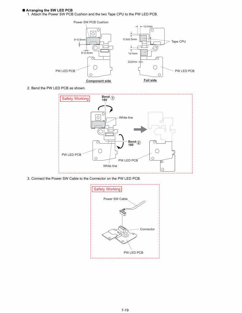
7-19
n Arranging the SW LED PCB1. Attach the Power SW PCB Cushion and the two Tape CPU to the PW LED PCB.
2. Bend the PW LED PCB as shown.
3. Connect the Power SW Cable to the Connector on the PW LED PCB.
0~0.5mm
Component side
0~0.5mm
0.5±0.5mm
1±1mm
2±2mm
1±1mm
Foil side
PW LED PCB PW LED PCB
Power SW PCB Cushion
Tape CPU
PW LED PCB
PW LED PCB
White line
White line
1
2
Bend180
Bend180
Safety Working
PW LED PCB
Connector
Power SW Cable
Safety Working

7-20
n Arranging the Power SW Cable
View "A"
SW LED PCB
Power SW Cable
Power SW Cable
Power SW Cable
Tape
Tape
CON Spacer
CON Spacer
Top Cabinet
Top Cabinet
CON Spacer
View "A"
View "B"
0~2mm
0~2mm
0~0.5mm
3~4mm
0~2mm
View "B"
0±0.5mm
Set the Cable along a connector side, not to prop.
Do not put up the Cable on the Cabinet.
Safety Working

7-21
7.2.8. Setting the IO PCB1. Fix the IO PCB using the six Screws<d>. No1 to No6
Note:Tighten the Screws in the numbered order (No1 to No6).
Screws <d>: DFHE5058ZB
n Arrange the IO FPC
<d>:No2
<d>:No3 <d>
:No4<d>:No5 <d>
:No6
<d>:No1
IO PCB
Rear I/O FPC Cover Sheet
View "B"
View "A"
View "A" View "B"
<No good>
2~3mm
R0.5~1.0mm
LID SW Cushion
IO FPC
R1.5~2.5mm
0±0.3mm
IO FPC
White line
Bend180
Bend90
White line
LID SW Cushion
LID SW Cushion
White line
White line
IO FPC
White lineWhite line
1~1.5mm
Bend180
Bend90
Bend90
Bend90
Front side Back side
0~0.5mm
0±0.5mm
0±0.5mm
Attention when bending the FPC1. Inside of bending should be from R0.5mm to
R1mm.2. Do not mistake the direction of bending.3. For bending point, it should be within 0.5mm from
the white line unless there is a regulation.
Safety Working

7-22
n Setting the IO FPC
n Setting the IO PCB and attaching the Rear I/O FPC Cover Sheet
IO PCB
IO FPC
FCC CN Stopper
Rear I/O FPC Cover Sheet
IO PCB
IO PCB
IO FPC
Rib
LID SW Cushion
Slot
Rib
Do not put up the IO FPC on the Rib.
Do not put up the Rear I/O FPC Cover Sheet on the Rib.

7-23
7.2.9. Setting the TP PCB1. Fix the TP PCB using the two Screws<c>. No1, No22. Connect the three Cables to the three Connectors on the
TP PCB (CN800, CN801, CN803).
Note:Tighten the Screws in the numbered order (No1, No2).
Screws <c>: DRHM0002ZA
n Attaching the Cable Sheet, Insulation Sheet and the Sheet1. Attach the Sheet and Insulation Sheet on the TP PCB.2. Attach the Cable Sheet on the Touch Pad FPC.
<c>:No1
<c>:No2
TP PCB
to Connector(CN800)
to Connector(CN801)
Connector CN801
Connector CN800
Connector CN803
to Connector(CN803)
Insulation Sheet
SheetTop Cabinet
Touch Pad FPC
Cable Sheet
TP PCB
LED FFC
Sheet
LED FFC
Rib of the Top Cabinet
Top Cabinet
TP PCB
Connectors
View "A"
View "A"
0~0.5mm
1~2mm
0~2mm
0~1mm
0~1mm
0~1mm

7-24
7.2.10. Setting the HDD Main FPC1. Fix the HDD Main FPC to the Batt HDD CN Angle using
the two Screws<a> and the two Screws<b>2. Fix the CN Spacer to the Batt HDD CN Angle using the
Screw<Z>.3. Fix the Batt HDD CN Angle using the Screw<Y>.
Screw <Y>: DFHE5092ZAScrew <Z>: DFHE5025ZAScrews <a>: DRHM5104ZAScrews <b>: DFHE5025XA
n Arranging the HDD Main FPC
<Y>
Battery Angle Sheet
Rib
MINI PCI Spacer
HDD Connector
EMP Sheet Batt HDD FPC
FPC Conduction Tape
View "A"
View "A"
<a>
<b>
<b>
<a>
Batt HDDCN Angle
Batt HDDCN Angle
HDD MainFPC
CN Spacer
<Z>
Battery Connector
Insulation Sheet
Press Set the Batt HDD CN Angle sliding to the left so that the HDD Main FPC does not attach to the Rib of the Top Cabinet.
HDD Main FPC
HDD Main FPC HD FPC Tape
Cable SheetCable Sheet
Sheet
<No good>
Sheet
White lineWhite line
White line
White line
White line
0~2mm
2~3mm
R0.5~1.0mm
1±1mm
1±1mm
0~1mm
0±0.5mm
Bend90
Bend180
Bend180
Bend180Bend
90Component side Foil side
Attention when bending the FPC1. Inside of bending should be from R0.5mm to R1mm.2. Do not mistake the direction of bending.

7-25
7.2.11. Setting the Main PCB, EXT Antenna PCB, PCMCIA Unit and RTC Battery1. Connect the Cable the Connector (CN4) on the Main
PCB, and Attach the RTC Battery.2. Fix the PCMCIA to the Main PCB using the Screws<T-2>.
No1 to No43. Connect the six Cables to the six Connectors.
(Main PCB: CN6, CN9, CN10, CN51, CN54)(EXT Antenna PCB: CN1)
4. Fix the Main PCB using the three Screws<V>. No5 toNo7
5. Fix the Main PCB using the two Screws<T-1>. No8, No96. Fix the Main PCB using the two Screws<S>. No10, No117. Fix the Main PCB using the Screw<W>. No128. Fix the Main PCB using the two Screw<X>. No13, No149. Fix the EXT Antenna PCB using the two Screws<U>.
No15, No16
Note:Tighten the Screws in the numbered order (No1 to No16).
Screws <S>: DFHM5054XAScrews <T-1>:DFHE5025XAScrews <T-2>:DFHE5025XAScrews <U>: DRQT2+G6FKLScrews <V>: DRHM5104ZAScrew <W>: DFHE5025ZAScrew <X>: DRHM5117ZA
<S>:No10
<S>:No11
<T-2>:No1
<T-2>:No2
<T-2>:No3
<T-2>:No4
<W>:No12
<T-1>:No8
<T-1>:No9
EXT Antenna PCB
ConnectorCN1
to Connector(CN4)
RTC Battery
Connector CN10(front side)
Connector CN51(front side)
Connector CN6(reverse side)
Connector CN9(reverse side)
Connector CN1(reverse side)PCMCIA Unit
to Connector(CN6)
to Connector
to Connector(CN9)
to Connector(CN950) to Connector
(CN51)
to Connector(CN54)
to Connector(CN10)
Connector CN4(reverse side)
Connector CN54(reverse side)
Main PCB
<X>:No13
<X>:No14
<U>:No16 <U>
:No15
<V>:No5
<V>:No7
<V>:No6
(EXT Antenna CN1)
to Connector(Main PCB CN1)

7-26
n Attaching the SD INS Sheet, Coil Cooling Sheet and MINI PCI Spacers
n Setting the LAN Cable and Modem Cable1. Set the LAN Cable and the Modem Cable to the DC/USB Cover Frame.2. Set the Clampers to the LAN Cable and the Modem Cable.3. Fix the DC/USB Cover Plate, the DC USB Cover Hook and the DC/USB Cover Frame using the two Screws<o>. No1, No2
Note:Tighten the Screws in the numbered order (No1, No2).
Screw <o>: DRHM5025YA
SD INS Sheet
Coil Cooling SheetIC
IC
MINI PCI Spacers
Ribs
DC/USB Cover Plate
DC/USB Cover Frame
DC/USB Cover Frame
Modem Cable
LAN Cable
Clampers
DC USB Cover Hook
<o>:No1
<o>:No2
Rib
The LAN Cable should be tied by the Clamper in its bottom.
Do not put up the DC/USB Cover Plate on the Rib of the Top Cabinet.
Safety Working
Safety Working

7-27
n Setting the Main PCB1. Set the Main PCB to the Top Cabinet in order.
View "C"
View "A"
View "B"
View "C"
View "A"
View "B"
Power SW Cable
Cable
Cable
Main PCB
LAN Cable
LAN Cable
Clamper
Clamper
Confirm that the tying point of the LAN Cable's Clamper is in the opposite direction to Main PCB.
Pass the Power SW Cable through the upper side of Cable.
Confirm that the Pin of the Top Cabinet of the hole of the Main PCB.
Pull out the LAN Cable
Confirm that the Pin of the Top Cabinet of the hole of the Main PCB.
Confirm that the Boss of the Top Cabinet of the hole of the Batt HDD CN Angle.
Pass the LAN Cable through this Slot.
Slot
Tying point
Main PCB
MP CN SpacerHole
Tip of the Screw Tip of the Screw
Hole
Slot
Batt HDD CN Angle
1
2
Safety Working
Safety Working
Safety Working

7-28
n Arranging the Cables and attaching the Sheets, the Tape, the Space PWB Hold MP and the Insulation Sheet1. Connect the five Cables to the five Connectors.
(Main PCB: CN6, CN9, CN10, CN51, CN54)2. Attach the three Sheets, the Tape, the Space PWB Hold MP and the Insulation Sheet.
View "A"
View "B"
View "C"
View "D"
View "A"
View "B"View "C"View "D"
0~1mm
Connect the Connector CN10.
Sheet
Sheet
Sheet
IO FPC
Tape
Insulation Sheet
Insulation Sheet
Space PWB Hold MP
Tape
Space PWB Hold MP
IC
Connect the Connector CN54.
Connect the Connector CN51.
Sheet
Sheet
CableCable
Connector CN51
Cable
Wireless Module Holder
0~1mm
0~1mm
1~2mm
0~1mm
3~4mm
Power SW CableCON SpacerTP PCB
0.5~1.5mm
0~0.5mm
1~2mm0~1mm
Do not put up the Cable on the Wireless Module Holder.
Attach the Sheet in condition that the IO FPC is slid to the side of the Connector CN10.
Pass the Cable through the right side of the Connector not to put up it on the Connector.
Safety Working
Connect the Connector CN6.
Connect the Connector CN9.

7-29
n Setting the RTC Battery1. Connect the Cable to the Connector CN4 on the Main PCB.2. Attach the RTC Battery to the Main PCB.
Connect the Connector CN4.
RTC BatteryGasketMain PCB
0~1mm
0~1mm
1~2mm1~2mm
1~2mm
Safety Working

7-30
7.2.12. Setting the PAD SW FFC Cover1. Set the Power Cable Guard. 2. Fix the PAD SW FFC Cover using the three Screws<R>.
No1 to No3
Note:Tighten the Screws in the numbered order (No1 to No3).
Screws <R>: DFHE5054XA
n Arranging the Power SW Cable
<R>:No1
<R>:No2
<R>:No3
PAD SW FFCCover
Power Cable Guard
Power Cable Guard
Main PCB
Power SW Cable

7-31
7.2.13. Setting the Wireless Module and SD PCB1. Attach the Memory Heat Plate to the Main PCB.2. Set the Wireless Module to the Main PCB.3. Attach the MINI PCI Protector Sheet to the
Wireless Module.4. Connect the Cable to the Connector (CN2) on the EXT
Antenna PCB. 5. Attach the CD Edge Sheet and the two MINI PCI Spacers
U2.6. Fix the SD PCB using the three Screws<Q>. No1 to No37. Connect the Cable to the Connector on the Main PCB.8. Attach the two Heat Dissipation Rubbers to the Main PCB.
Note:Tighten the Screws in the numbered order (No1 to No3).
Screws <Q>: DFHE5025XA
n Attach the MINI PCI Protector Sheet, the CD Edge Sheet, the MINI PCI Spacers U2 and the Heat Dissipation Rubbers
Main PCB
Connector CN2
EXT Antenna PCB
Connector
SD PCB
<Q>:No1
<Q>:No2
<Q>:No3
to Connector(CN2)
to Connector(CN952)
Wireless Module
Memory Heat Plate
Heat Dissipation Rubbers
MINI PCI ProtectorSheet
MINI PCI Spacer U2
MINI PCI Spacer U2
CD Edge Sheet
Confirm that the Insulation Sheet is attached between the SD PCB and the Main PCB.
Safety Working
View "B"
View "D"
View "E"
View "C"
View "A"
View "C"
View "A"
View "B"
View "D" View "E"
0~0.5mm0~1mm
0~0.5mm
0~1mm
2~3mm
0~0.5mm
0~0.5mm
4±1mm
1.5~5.5mm
Wireless Module
Heat Dissipation Rubber
Heat Dissipation Rubber
Heat Dissipation Rubber
IC
2~3mm
0.5~2.5mm
Heat Dissipation Rubber
IC
Main PCB
MINI PCI ProtectorSheet
MINI PCI Protector Sheet
MINI PCI Protector Sheet
MINI PCI Spacer U2
MINI PCI Spacer U2
MINI PCI Spacer U2
MINI PCI Spacer U2
CD Edge Sheet
CD Edge Sheet
Safety Working Safety Working Safety Working

7-32
n Attaching the Memory Heat Plate
7.2.14. Setting the Speaker1. Set the MP Eject Slide Assy to the Bottom Cover.2. Fix the MP Eject BOUSUI Plate using the Screw<P>.3. Fix the MP Eject Lever using the four Screws<O>.4. Fix the Heat Pipe Unit Bottom using the two Screws<N>.5. Fix the three Speaker Angles to the Speaker using the
three Adhesive Tapes.6. Attach the Speaker Spacer to the Speaker.7. Attach the CPU Heatsink Rubber and the LAN Heat Plate
Spacer to the LAN Heat Plate.8. Fix the Speaker and the LAN Heat Plate using the four
Screws<M>.9. Attach the Radiation Rubber, Coil Cooling Sheet and the
LCD Lamp Sheet to the LAN Heat Plate.
Screws <M>: DXQT26+D4NLTScrews <N>: DXYN+J6FNLScrews <O>: DXYN26+F5NLTScrew <P>: DXQT26+D4NLT
0~1mm
0~1mm
IC
Memory Heat Plate
<O>
<P>
<N><N>
<M>
<O><O>
<O>
<M>
<M><M>
MP EjectLever
MP Eject BOUSUI Plate
MP Eject Spring
LAN Heat Plate
Radiation Rubber
CPU HeatsinkRubber
Heat Pipe UnitBottom
MP Eject Slide Assy
DIMM Stopper Sheet
SpeakerSpacer
Speaker
Speaker Angle
LAN Heat Plate Spacer
Adhesive Tape
Bottom Cover
LCD Lamp Sheet
Coil Cooling Sheet

7-33
7.2.15. Setting the DIMM Cover and Bottom Cover1. Set the Bottom Cover.2. Connect the Cable to the Connector (CN12) on the Main
PCB. 3. Fix the Bottom Cover using the eight Screws<L>. No1 to
No84. Fix the Bottom Cover using the eight Screws<K>. No9 to
No165. Attach the DIMM Radiation Sheet.6. Fix the DIMM Cover using the four Screws<J>. No17 to
No20
Note:Tighten the Screws in the numbered order (No1 to No20).
Screws <J>: DRQT26+D4FZLTScrews <K>: DRQT26+D4FZLTScrews <L>: DRSB3+8FKL
n Arranging the DIMM Cover and the DIMM Radiation Sheet
<J>:No19
<J>:No20
<J>:No17
<J>:No18
<K>:No9
<K>:No10 <K>
:No11
<K>:No12
<K>:No13
<K>:No14
DIMM Cover
DIMM Radiation Sheet
Bottom Cover
Lock Plate
Main PCBConnector CN12
to Connector(CN12)
<L>:No1
<L>:No2
<L>:No3
<L>:No7
<L>:No8
<L>:No6
<L>:No5
<L>:No4
<K>:No15
<K>:No16
DIMM Cover
DIMM Cover Spacer
DIMM Cover Spacer
DIMM Stopper
DIMM Stopper Spacer
DIMM Radiation Sheet
Sheet
Sheet
View "A"
View "A" View "B"
View "B"
0~2mm
0~2mm
5±2mm

7-34
7.2.16. Setting the KBD PCB, MDC Modem and LCD Cable/MIC Frame1. Connect the three Cables to the three Connectors
(CN930, CN950, CN952) on the KBD PCB.2. Fix the KBD PCB using the two Screws<H>. No1, No23. Connect the Cable to the Connector (J2) on the MDC
Modem. 4. Attach the Sheet to the MDC Modem.5. Fix the MDC Modem using the two Screws<I>. No3, No46. Attach the LCD Conductive Sheet and the Gasket to the
LCD Cable/MIC Frame.7. Set the LCD Cable/MIC Frame to the Top Cabinet.
Note:Tighten the Screws in the numbered order (No1 to No4).
Screws <H>: DFHE5025XAScrews <I>: DFHE5025XA
n Attaching the Sheet to the MDC Modem1. Connect the Cable to the Connector (J2) on the MDC Modem.2. Attach the Sheet to the MDC Modem.
<H>:No1
<H>:No2
<I>:No3 <I>
:No4
Connector CN950(front side)
Connector CN930(reverse side)
MDCModem
Sheet
KBD PCB
Connector CN952(reverse side)
to Connector(CN950)
to Connector(CN952)
LCD Cable/MIC Frame
LCD ConductiveSheet
Gasket
to Connector(J2)
Connector J2 (reverse side)
Connector J1 (reverse side)
to Connector(CN930)
Top Cabinet
Place the Cable not to pass through this range.
View "A"
View "A"
3~4mm
5~7mm
Sheet
Cable
MDC Modem
Connector (J2) Sheet
Cable
MDC Modem
Connector (J2)
Safety Working

7-35
n Arranging the Cables and setting the LCD Cable/MIC Frame1. Pass the LCD Cable and Antenna Cables through the LCD Cable/MIC Frame.2. Attach the LCD Conductive Sheet and the Gasket to the LCD Cable/MIC Frame.3. Set the LCD Cable/MIC Frame to the Top Cabinet.
View "A" View "B"
View "A"
View "B"
LCD ConductiveSheet
LCD ConductiveSheet
LCD ConductiveSheet
LCD Cable/MIC Frame
LCD Cable and Antenna Cable
LCD Cable/MIC Frame
LCD Cable/MIC Frame
LCD Cable
LCD Cable
Pass the LCD Cable and the two Antenna Cables through the LCD Cable/MIC Frame.
Antenna Cables
Gasket
Gasket
Gasket
Antenna Cables
Top Cabinet
Safety Working

7-36
7.2.17. Setting the KB Cable Cover, Keyboard and PCMCIA Protector1. Fix the PCMCIA Protector using the five Screws<G>. No1
to No62. Connect the two Cables of the Keyboard to the two Con-
nectors (CN932, CN933) on the KBD PCB.3. Set the Keyboard.4. Fix the KB Cable Cover using the five Screws<F>. No7 to
No11
Note:Tighten the Screws in the numbered order (No1 to No11).
Screws <F>: DRHM0002ZAScrews <G>: DRQT2+I35FKL
n Arranging the Keyboard1. Attach the KB Spacer Sheet and the two Gaskets to the Keyboard.
<F>:No7
<F>:No8
<F>:No9
<F>:No10
<F>:No11
Keyboard
KB PCB
Connector(CN933)
to Connector(CN933)
KB Cable Cover
Connector(CN932)
to Connector(CN932)
<G>:No1
<G>:No2
<G>:No3
<G>:No4
<G>:No5<G>
:No6
PCMCIA Protector
Keyboard KB Spacer Sheet
KB Spacer Sheet
Gasket
0~1mm0~1mm
View "A"View "B"
Gasket
View "A"
Gasket
0~0.5mm
KB Spacer Sheet
View "B"
Gasket
0~0.5mm

7-37
7.2.18. Setting the KB Cover, Hinge Cover L, Hinge Cover R and Keyboard1. Insert the front hooks of the Keyboard to the Top Cabinet
in order, and set the Keyboard.2. Fix the Hinge Cover L and R using the four Screws<C>.
No1 to No43. Fix the Hinge Cover L and R using the four Screws<D>.
No5 to No84. Fix the KB Cover using the four Screws<B>. No9 to No12
Note:Tighten the Screws in the numbered order (No1 to No12).
Screws <B>: DRQT26+D4FZLScrews <C>: DFHE5054XAScrews <D>: DFHE5054XA
<B>:No9
<B>:No10 <B>
:No11
<B>:No12
<C>:No1
<C>:No3
<C>:No2
<C>:No4
<D>:No6
<D>:No7
<D>:No8
<D>:No5
KB Cover
Front hook
Hinge Cover L
Hinge Cover R
Keyboard
12
3
4
5

7-38
7.2.19. Setting the HDD1. Set the HDD FPC to HDD.2. Attach the Heater to HDD.3. Attach the Heater Sheet to the Heater.4. Attach the two Sheets to HDD.5. Attach the six HDD Forming MFYPC and the two HDD
Terminal Plate Upper to the HDD Damper Assy6. Attach the six HDD Forming MFYPC and the two HDD
Terminal Plate Upper to the HDD Damper Assy.7. Set the HDD Damper Assy to HDD.8. Attach the Side Cushion to the HDD L Case Assy.9. Set the HDD U Case Assy and the HDD L Case Assy,
and set the two Tabs of the HDD L Case Assy.10. Fix the HDD U Case Assy and the HDD L Case Assy
using the four Screws<A>.
Screws <A>: DFHE5025XA
n Attaching the Sheet
<A>
<A><A>
<A>
Heater Sheet
HDD U Case Assy
HDD FPC
Heater
HDD TerminalPlate Upper
HDD TerminalPlate UpperSide Cushion
HDD Forming MFYPC
SheetSheetHDD Forming MFYPC
HDD Forming MFYPC
HDD U Case Assy
Tab
Tab
HDDHDD DamperAssy
Cables
Cables
Heater
HeaterHeaterHeater
Heater
Heater
Heater Sheet
HDD FPC
HDD FPCHDD FPCHDD
Terminal
HDD FPC
HDD
HDD
Sheet
Sheet
Sheet
Heater Sheet
0~2mm
0~2mm
0~2mm
0~2mm
View "D"View "A"
View "E"View "C"
View "B"
View "A"
View "B"
View "C"View "D"View "E"
Sheet
SheetSheet
Sheet
Do not put the Cables between the Heater and the HDD.
Safety Working

7-39
7.2.20. Setting the Battery Pack, the HDD Pack and the FDD Pack1. Set the FDD Pack.2. Set the HDD Pack.3. Set the Battery Pack.
MPCover
BatteryCover
HDD Cover
HDD Pack
FDD Pack
Battery Pack

CF-29NTQGZBM
8 Exploded ViewK74
K75K73
K17K409
K68
K25
E45E9
K452
E47
K22
K409
K27
K93
K409E19
K400
K69
K409
K26
K99
K70
K4
K463
K54
E3E46
K405
E4
E14
K21
K21K36
K409
K409
K61
K461
K1-11K1-1
K1-9
K1-6
K1-3K1-13
K1-14
K1-13
K1-2
K1-2K1-8
K1-8
K1-10
K1
E13
K457
K400
K406
K406K64
K65
K406K406
K2
K72
K785
K785
K8
K787
K786K787
K787
K1-12 K1-12
K1-15
A
LLL
B
B
B
B
BB
A
A
A
A
F
V
V
Screw tightening torque 0.19 _ 0.02 N.m (2.0 _ 0.2 kgf.cm) 0.45 _ 0.05 N.m (4.5 _ 0.5 kgf.cm) 0.49 _ 0.05 N.m (5.0 _ 0.5 kgf.cm) 1.47 _ 0.20 N.m (15 _ 2.0 kgf.cm) 0.18 _ 0.22 N.m (2.0 _ 0.2 kgf.cm) 0.2 _ 0.02 N.m (2.0 _ 0.2 kgf.cm)
A
B
F
G
I
L
++++++
++
++
++

CF-29NTQGZBM
K2-8
K2-8-7
K2-8-7K2-8-3
K2-8-1
K2-8-2K2-8-1
K2-22
K2-22
K2-8-7
K2-8-5
K2-8-4K2-8-6 K2-31 K2-11
K2-11-3
K2-11-1
K2-11-2
K2-11-4K2-21
K2-21
K2-30
K2-30
K2-5K2-4
K2-33
K2-14
K2-18
K2-23
K23
K2-22
K2-3
K2-2
K2-1
K2-1-3K2-1-2K2-1-1
K2-26
K2-24K2
K2-17
K2-15
K2-16
K2-24
K33
K39K18
K400
K412
K20
K2-13-3
K2-32K2-12
K2-13
K2-13-2
K2-13-1K2-13-4
K2-31
K2-12-2
K2-22
K2-12-1
K2-12-5
K2-12-4
K2-12-3
K2-7-3
K2-7-1
K2-7-1
K409
K16
K2-9-6 K2-9-5
K2-9-11
K2-9-11K2-9-1
K2-9-1
K2-22 K2-9-7
K2-22
K2-9-4
K2-9-3
K2-9-8
K2-9-9
K2-9
K2-9-10K2-9-9
K410
K40
K32K34
K35
K410K41
K410E48E49
K31
K2-6-3
K2-6-2
K2-6
K2-22
K2-22
K2-6-1
K2-6-1
K2-10-3
K2-10-2
K2-10-1
K2-10-1
K2-10
K2-27
K2-3
K2-9-2
K2-41
K2-41
K2-42
K866
K2-7-4
K2-9-12
K2-9-12
K2-43
K2-43
K2-10-4
L
B
B B
F
B
BB
B
B
L
P
B
L
LB
B
B
B
B
LL
A
P
AB
B
B
B
A
A
G
G
B
B
L
Screw tightening torque 0.19 ± 0.02 N.m (2.0 ± 0.2 kgf.cm) 0.45 ± 0.05 N.m (4.5 ± 0.5 kgf.cm) 0.49 ± 0.05 N.m (5.0 ± 0.5 kgf.cm) 1.47 ± 0.20 N.m (15.0 ± 2.0 kgf.cm) 0.18 ± 0.02 N.m (2.0 ± 0.2 kgf.cm) 0.2 ± 0.02 N.m (2.0± 0.2kgf.cm) 0.8 ± 0.1 N.m (8.0 ± 1.0 kgf.cm)
A
B
F
G
I
L
P
K2-7-2
K2-7

CF-29NTQGZBM
K309
E32-03
K306
K304
K308
K313
K303
K304
K316
K313K311K305
K311E32-02
K316
K315
E32-01
K314
K311
K310
K316
K316
E32
K312
K301
K302
K403K412
K408 K464
K403
K46
K778
E12
K19
K409
K409K7
K43
E6
K458
K24
E8
E2
E15
K37
K99
K38
K45
K5
E50
K83
K80
K450
K52
K460
K462
K6
E7
K8K408
K405
K87
K409
K55
K405
K405 K15
E43K405
K86
K405
K92K861
K861
K862 K92
K99
E1
K51
K90
K405K405
K861K406
K406
K7
K783
K2
E44
K465
K81
K52
E41
E42
K773
K405
K770
K51K784
K7
K858
K859
K405
K860E789
E790
K405
K405
K863
K864
BT
K778
K865
K870
K869K868
K871
K872
K7
K873
K879
K7
N
N
H F
A A
H
A
F
F
E
A
A
A
AN
N
AA
A
GA
FA
A
A
P
G
G
E
C
A
A
Z
Z
A
A
Y
Y
A
W
W
Screw tightening torque 0.19 _ 0.02 N.m (2.0 _ 0.2 kgf.cm) 0.216 _ 0.0196 N.m (2.2 _ 0.2 kgf.cm) 0.314 _ 0.0196 N.m (3.2 _ 0.2 kgf.cm) 0.49 _ 0.05 N.m (5.0 _ 0.5 kgf.cm) 0.441 _ 0.049 N.m (4.5 _ 0.5 kgf.cm) 1.47 _ 0.20 N.m (15 _ 2.0 kgf.cm) 1.30 _ 0.17N.m (13 _ 2.0 kgf.cm) 0.18 _ 0.02 N.m (2.0 _ 0.2 kgf.cm) 0.2 _ 0.02 N.m (2.0 _ 0.2 kgf.cm) 0.45 _ 0.03 N.m (4.5 _ 0.3 kgf.cm) 0.8 _ 0.1 N.m (8.0 _ 1.0 kgf.cm)
A
C
E
F
G
H
I
L
M
N
P
+++
+++
++++
++
+++
++
++
++
+

CF-29NTQGZBM
K3
K3-11
K3-15
K3-12
K3-16
K3-14
K3-6K3-13
K3-14
K3-8
K3-7K3-2
K3-9K3-14
K3-14
K3-9
K3-14
K3-10
K3-10
K3-10
K3-3K3-17
K3-18K3-18
K402
K400
K400
K402K402
K402 K400
K400K400
K402
K402K56
K7
K466K467
K57
K400K400
K47
K13
K13
K13
K13
K11
K50
K49
K48
K2
K3-11
K3-21
K3-20
K3-26K3-26
K3-22
K3-14
K3-24K3-25
K3-23
K880
K882K883
K881
K884
K894
K893
K
B
E
E
E
E
E
K
B
K
K
BK
B
B
K
BB
E
E
E
X
X
Screw tightening torque 0.19 _ 0.02 N.m (2.0 _ 0.2 kgf.cm) 0.45 _ 0.05 N.m (4.5 _ 0.5 kgf.cm) 0.49 _ 0.05 N.m (5.0 _ 0.5 kgf.cm) 0.8 _ 0.1N.m (8.0 _ 1.0 kgf.cm)
A
B
E
K
++++++
++

CF-29NTQGZBM
E18
K206
K205
K238
K200
K200-6
K200-6-1
K200-6-2
K200-1
K235
K200-11K404K200-12
K200-13
K200-14
K200-1-5
K200-1-2
K200-1-3
K200-1-5
K200-6-1-1
K236
K404
K204
K239
K238
K239
K200-19
K7
K876
K876
GA
G
G
G
A
Screw tightening torque 0.19 _ 0.02 N.m (2.0 _ 0.2 kgf.cm) 0.45 _ 0.50 N.m (4.5 _ 0.5 kgf.cm) 0.441 _ 0.049 N.m (4.5 _ 0.5 kgf.cm) 1.47 _ 0.20 N.m (15 _ 2.0 kgf.cm) 1.30 _ 0.17N.m (13.0 _ 2.0 kgf.cm)
A
B
F
G
H
+++++
++++
+

CF-29NTQGZBM
E18
E17
Kapton Tape
E18-5
E18-3
E18-4
E18-6
E18-7
E18-6
E18-7
E18-1
E18-10
E18-10
E18-8
K225
K249
K248
K237
E5
K237
K877
K230
K261
K260
E16
K875
K874
K877
K237
K878 Screw tightening torque 0.19 _ 0.02 N.m (2.0 _ 0.2 kgf.cm) 0.45 _ 0.05 N.m (4.5 _ 0.5 kgf.cm) 0.216 _ 0.0196 N.m (2.2 _ 0.2 kgf.cm) 0.314 _ 0.0196 N.m (3.2 _ 0.2 kgf.cm) 0.49 _ 0.05 N.m (5.0 _ 0.5 kgf.cm)
A
B
C
D
E
++++
++
++++

CF-29NTQGZBM
K222
K66
K67
E40
K451
K451
E11
E20
K222
K222
K222
K201-1-6
K201-1-4 K201-1
K201
K201-1-2
K202K202-1
K203
K222K222
K223
K228
K201-9
K201-1-5
K222
K201-1-6K223
K222K201-1-3
K222
E10
K215
K211K246
K222
K222
O
O
O
O
OG
O
O
O
O
O OG
O
O
Screw tightening torque 0.19 _ 0.02 N.m (2.0 _ 0.2 kgf.cm) 0.45 _ 0.05 N.m (4.5 _ 0.5 kgf.cm) 0.216 _ 0.0196 N.m (2.2 _ 0.2 kgf.cm) 0.314 _ 0.0196 N.m (3.2 _ 0.2 kgf.cm) 1.47 _ 0.20 N.m (15 _ 2.0 kgf.cm) 0.49 _ 0.05 N.m (5.0 _ 0.5 kgf.cm)
A
B
C
D
G
O
+++++
++
+++++

9 Replacement Parts List Note: Important Safety Notice Components identified by mark have special characteristics important for safety. When replacing any of these components, use only manufacturer's specified parts.CF-29NTQGZBMREF.NO. and AREA PART NO. DESCRIPTION Q'TYMain Block UnitE1 DL3UPB465GRA PCB, MAIN RTL 1E2 DL3U1B266CRA PCB, IO RTL 1E3 DL3U2B266CRA PCB, LED RTL 1E4 DL3U3B266CRA PCB, KBD RTL 1E5 DL3U4B266CRA PCB, TS RTL 1E6 DL3U5B266CRA PCB, TP RTL 1E7 DL3UP1269ARA FPC, HDD-MAIN 1E8 DL3UPB270ARA FPC, IO 1E9 DL3UP1271BRA FPC, SW-LED 1E10 DL3U11331ARA PCB, W-LAN ANT R RTL 1E11 DL3U21331ARA PCB, W-LAN ANT L RTL 1E12 DL3UP1336ARA PCB, EXT ANT RTL 1E13 N3CABTD00006 HDD 1E14 DFJK50U092BB KB CN FFC 1E15 DFJK9007ZA TP SW FFC 1E16 N0GF1J000007 INVERTER 1E17 DFJS875XA LCD CABLE 1E18 DFWV08A0072 LCD UNIT ASS'Y 1E18-1 DL3DE0177ARA LCD ASS'Y 1E18-3 DFHG874ZA LCD SIDE DAMPER UN 1E18-4 DFHG850YA LCD SIDE DUMPER R13 1E18-5 DFHG884ZA LCD DAMPER FRONT 1E18-6 DFHG852ZA TS SPACER L13 2E18-7 DFHG853ZA TS SPACER S13 2E18-8 DFMY0409ZA LCD THERMAL PLATE 1E18-10 DFMY0348ZB LCD LAMP SHEET 2E19 N2ABZJ000033 KEYBOARD 1E20 DFJS868ZA CABLE (BLACK), ANT PCB R 1E40 DFJS869ZA CABLE (GRAY), ANT PCB L 1E41 DFJS870ZA CABLE (BLACK), KB PCB 1E42 DFJS871ZA CABLE (GRAY), KB PCB 1E43 N5HAZ0000013 MDC MODEM 1E44 N5HZC0000014 WIRELESS LAN MODULE 1E45 N2EABEC00006 TOUCH PAD 1E46 DFJK10T017BB LED 6 FFC 1E47 DFJS865ZA POWER SW CABLE 1E48 DFJS866ZA MODEM CABLE 1E49 DFJS978ZA LAN CABLE 1E50 K1NBD6A00006 PCMCIA EJECTOR 1E789 DL3UPB484ARA PCB, SD-CN RTL 1E790 DFJK12T034DB FFC, PAD 1AccessoriesA1 CF-AA1653AM4 AC ADAPTER 1A2 K2CG3DR00003 AC CABLE 1A3 DFQX5556YB MANUAL 1A5 CGR-B/982A BATTERY PACK 1A6 DFJS954ZA MODEM CABLE 1A7 DFHS9017ZA CLOTH, TOUCH PANEL 1A8 DFHR9084YA PEN 1Packing Material

P1 DFPK1154LA PACKING CASE 1P2 DFPE0611ZA MANUAL HOLDER 1P3 DFPN0754XA CUSHION 1Mechanical PartsK1 DFWV99A0105 HDD MOUNTING KIT 1K1-1 DL3UP1268ARA FPC, HDD 1K1-2 DFHE5025XA SCREW 4K1-3 DFHG1696ZA LCD DUMPER 2K1-6 DFHR8489ZA HDD DAMPER ASS'Y 1K1-8 DFMY3143YA HDD THERMAL PLATE UPPER 2K1-9 L9DZAA000004 HEATER 1K1-10 DFMD8038ZA HDD L CASE ASS'Y 1K1-11 DFMD8039ZA HDD U CASE ASS'Y 1K1-12 DFMX0634ZA SHEET 2K1-13 DFHG1750ZA HDD FORMING MFYPC 4K1-14 DFHR8482YA SIDE CUSHION, HDD 1K1-15 DFHR3C10ZA SHEET, HEATER 1K2 DFKM8179YC-0 TOP CABINET ASS'Y 2 1K2-1 DFBD9005ZA-1 POWER SW ASS'Y 1K2-1-1 DFUQ0099ZA POWER SW SPRING 1K2-1-2 DFBD0168ZA-1 POWER SW KNOB 1K2-1-3 DFHR6069ZA-1 POWER SW ARM 1K2-2 DFHR6126YA-0 WM SW COVER 1K2-3 DFHM0352ZA LCD FOOT CAP 2K2-4 DFKE0732WA-0 HDD LATCH LEVER 1K2-5 DFKE0733VA-0 HDD LATCH COVER 1K2-6 DFKE8182YA-0 PC COVER ASS'Y 2 1K2-6-1 DFBH3033ZB LID HINGE 2K2-6-2 DFGE0119ZA-0 PC COVER SHEET SD 1K2-6-3 DRQT26+D3FKL SCREW 2K2-7 DFKE8181ZA-0 MP COVER ASS'Y 2 1K2-7-1 DFBH3033ZB LID HINGE 2K2-7-2 DFGE0116ZA-0 MP COVER SHEET 2 1K2-7-3 DRQT26+D3KLT SCREW 2K2-7-4 DFHR3B69ZA CUSHION, MP COVER 1K2-8 DFKE8180ZA-0 CN COVER ASS'Y 2 1K2-8-1 DFBH3033ZB LID HINGE 2K2-8-2 DFGE0082XA-0 CN COVER SHEET R 1K2-8-3 DFGE0081ZA-0 CN COVER SHEET L 1K2-8-4 DFKE9062YA-0 CN SLIDE COVER 1K2-8-5 DFHR3527XA CN PACKING-SLIDE 1K2-8-6 DFMD1165YA CN WATER PROOF PLATE 1K2-8-7 DRQT26+D3KLT SCREW 3K2-9 DFKE8184ZA-0 BATT COVER ASS'Y 2 1K2-9-1 DFBH3033ZB LID HINGE 2K2-9-2 DFGE0083YA-0 BATT COVER SHEET 1K2-9-3 DFHM0310YA WASHER 2K2-9-4 DFHM0327YA BATT LATCH ANGLE 1K2-9-5 DFHR3466YA LID KNOB SHEET 1K2-9-6 DFKE0799ZA-0 LID KNOB 1K2-9-7 DFUN0068XA LID KNOB SPRING 1K2-9-8 DFUS0292ZB LID KNOB SPRING PLATE 1K2-9-9 DRHM5025YAT SCREW 2K2-9-10 DXQT2+F3FNLT SCREW 1K2-9-11 DRQT26+D3KLT SCREW 2K2-9-12 DFHR3B71ZA CUSHION, BATT COVER 2K2-10 DFKE8183ZA-0 HDD COVER ASS'Y 2 1K2-10-1 DFBH3033ZB LID HINGE 2

K2-10-2 DFGE0084ZA-0 HDD COVER SHEET 1K2-10-3 DRQT26+D3KLT SCREW 2K2-10-4 DFHR3697ZAT HDD COVER CUSHION 2K2-11 DFKE8177ZA-0 PC LATCH ASS'Y 2 1K2-11-1 DFBD0185ZA-0 PC LATCH LEVER 2 1K2-11-2 DFMD1161ZA PC LATCH ANGLE 1K2-11-3 DFUQ0089YA SPRING (MP/PC LATCH) 1K2-11-4 DRHM5025YA SCREW 3K2-12 DFKE8176ZA-0 MP LATCH ASS'Y 2 1K2-12-1 DFBD0170WA-0 MP LATCH LEVER 1K2-12-2 DFKE0811ZA-0 MP LATCH CASE 2 1K2-12-3 DFMD1162ZB MP LATCH ANGLE 1K2-12-4 DFUQ0089YA SPRING (MP/PC LATCH) 1K2-12-5 DRHM5025YA SCREW 3K2-13 DFKE8175ZA-0 CH LATCH ASS'Y 2 1K2-13-1 DFBD0184ZA-0 CN LATCH LEVER 2 1K2-13-2 DFKE0810ZA-0 CN LATCH CASE 2 1K2-13-3 DFUQ0108ZA SPRING, CN LATCH 1K2-13-4 DRHM5025YAT SCREW 1K2-14 DFKE9068ZA-0 HDD LATCH LOCK ASS'Y 1K2-15 DFKH8008YA-0 HANDLE ASS'Y 2 1K2-16 DFKX0049YA-0 HANDLE BASE L 1K2-17 DFKX0050XA-0 HANDLE BASE R 1K2-18 DFMD7938WA TOP LIB ANGLE CPU 1K2-21 DFUQ0102ZA POTRE SPRING 2K2-22 DRQT26+D3KLT SCREW 12K2-23 DRSB26+4FKLT SCREW 2K2-24 DRSB4+8FKLT SCREW 2K2-26 DFHR3497YA POWER SW SHEET 1K2-27 DFHR3524ZA KB CABLE CUSHION 1K2-30 DXQT3+F4FNLT SCREW 2K2-31 DFHE5121YA SCREW 6K2-32 DXQT26+D4NLT TW SCREW 2K2-33 DFGE0097ZA-0 HDD LATCH LOCK CASE SHEET 1K2-41 DFGE0102ZA-0 SHEET, REAR BELT COVER 2K2-42 DFGE0104ZA-0 SHEET(USB), TOP REAR COVER 1K2-43 DFHG1699ZA LCD LOCK SHEET 2K3 DFKF8162YA-0 BOTTOM CABINET ASS'Y 2 1K3-2 DFHG3526YA MP EJECT PACKING-SLIDE 1K3-3 DFHG3528ZA SPEAKER SPACER 1K3-6 DFHR6083XA-0 MP EJECT LEVER 1K3-7 DFKE8166ZA-0 MP EJECT SLIDE ASS'Y 1K3-8 DFMD1164ZA MP EJECT PLATE 1K3-9 DFMD7945ZA HEAT PIPE BOTTOM ANGLE 2K3-10 DFMS0019ZA SPEAKER ANGLE 3K3-11 DFMY0414ZA CPU HEAT PIPE RUBBER 2K3-12 DFMY9023WA HEAT PIPE UNIT BOTTOM 1K3-13 DFUW0064YAT MP EJECT SPRING 1K3-14 DXQT26+D4NLT SCREW 7K3-15 DXYN26+J6FNL SCREW 2K3-16 DXYN26+F5NLT SCREW 4K3-17 L0AA04A00023 SPEAKER 1K3-18 DFHP7163ZA ADHESIVE TAPE, SP 3K3-20 DFUS0299ZAT EMI SPRING 1K3-21 DFMC0406ZAT EMI GASKET HDD 1K3-22 DFMC0685ZAT GASKET SHEET 1K3-23 DFMY0248YA CPU HEATSINK RUBBER 1K3-24 DFMY3212ZA LAN HEAT PLATE 1

K3-25 DFHR3B66ZA LAN HEAT PLATE SPACER 1K3-26 DFHR3B67ZA HEAT PIPE SPACER 2K4 DFMC0685ZA CONDUCTIVE SHEET, LCD 1K5 DFMD7929XA TOP RIB ANGLE FRONT 1K6 DFMD9090XA BATT HDD CN ANGLE 1K7 DFMX0635ZB SHEET 7K8 DFMX1006ZA CABLE SHEET 2K11 DFGT1055ZA BOTTOM COVER SHEET A 1K13 DFHG370ZA FOOT RUBBER 4K15 DFHP7162ZA HD FPC TAPE 1K16 DFGE0077ZA-0 WM COVER 1K17 DFGP0198ZB-0 PALM TOP COVER SHEET 1K18 DFHG1734ZA-0 SERIAL CN COVER 1K19 DFHG830ZA CON SPACER 1K20 DFHR3C26ZA SERIAL CN LID PLATE 1K21 DFHP7140ZA TAPE CPU 2K22 DFHP7160YA PW LED SHEET 1K23 DFHR1012ZA CLAMPER 2K24 DFHR3529YA LID SW CUSHION 1K25 DFHR3560YB TOUCH PAD ADHESION SEAT 1K26 DFHR3619ZA LEDX6 SPACER SHEET 1K27 DFHR3643ZA TP BOTTOM TAPE 1K31 DFHR6065WA DC/USB CN COVER FRAME 1K32 DFHR6180ZA-0 DC COVER 1K33 DFHR6090XA-0 SERIAL CN CAP 2 1K34 DFHR6181ZA-0 USB COVER 1K35 DFHR6104WA-0 LAN CN COVER 1K36 DFHR6107YA LED SPACER SHEET 1K37 DFHR6108ZA-0 REAR I/O FPC COVER SHEET 1K38 DFMC0406XA GASKET FOR MP 1K39 DFMD4045ZA SERIAL COVER PLATE 1K40 DFMD4048ZA DC/USB COVER LID PLATE 1K41 DFMD7960ZA DC/USB COVER PLATE 1K43 DFMX0702ZA INSULATION SHEET 1K45 DFUS0296ZA MP FINGER 1K46 DFUS0297ZA USB SHIELD SPRING 1K47 DFGE0078ZA-0 SPEAKER NET 1K48 DFGE0085ZA-0 BOTTOM COVER SHEET B 1K49 DFGE0086YA-0 BOTTOM COVER SHEET C 1K50 DFGE0087ZA-0 BOTTOM COVER SHEET D 1K51 DFHR3445ZA HEAT DISSIPATION RUBBER 2K52 DFHR3713ZA MINI PCI SPACER U2 3K54 DFHR6068ZA LCD CABLE/MIC FRAME 1K55 DFHR6084YA PAD SW FFC COVER 1K56 DFHR6117WA DIMM RADIATION SHEET 1K57 DFKE8173YB-0 DIMM COVER ASS'Y 2 1K61 DFKE0808ZA-0 KB CABLE COVER 1K64 DFKE0714YA-0 HINGE COVER L 1K65 DFKE0715YA-0 HINGE COVER R 1K66 DFKE0739YA-0 ANTENNA PCB COVER R 1K67 DFKE0740YA-0 ANTENNA PCB COVER L 1K68 DFGE0075UA-0 PALM TOP COVER 1K69 DFGE0076YA-0 KB COVER 1K70 DFHR6064ZA TOUCH PAD SW KNOB IN 1K72 DFHR3523WA KB SPACER SHEET 1K73 DFQT0045ZA ENERGY STAR LABEL 1K74 DFQT9974ZA WINDOWS XP LABEL 1K75 DFQT9948ZA CENTRINO LABEL 1

K80 DFMX1102XA PC PLATE SHEET 1K81 DFHR3A32ZA MINI PCI PROTECTOR SHEET 1K83 DFMY9032ZA PCMCIA HEAT P ASS'Y 1K86 DFHM0304YB MDC SPACER 2K87 DFHM0330YB CN SPACER 1K90 DRHM5118ZA SCREW 2K92 DFHR3713ZA MINI PCI SPACER U2 2K93 DFHG0306ZA-0 TOUCH PAD SW KNOB 1K99 DFHR3741ZA FFC CN STOPPER 3K200 DFWV80A0352 LCD FRONT CABINET/TS PANEL ASS'Y 1K200-1 DFKF8163ZA-0 LCD FRONT CABINET 2 1K200-1-2 DFBH3027YA HINGE L 1K200-1-3 DFBH3028YA HINGE R 1K200-1-5 DXSB4+6FNLT SCREW 2K200-6 DFWV84A0259 TOUCH SCREEN PANEL KIT 1K200-6-1 DL3DV0177ARA TOUCH SCREEN PANEL 1K200-6-1-1 DFHR9068ZA PROTECTIVE FILM 1K200-6-2 DFHP7183ZA TS TAPE 13 L 1K200-11 DFHR3702ZA TS FFC SHEET 1K200-12 DFHE0829ZA LID MAGNET 1K200-13 DFHG1706ZA FORMING U 1K200-14 DFQT9664ZA-1 TOUGH BOOK LABEL (W) 1K200-19 DFHR3695ZA TS FPC SPACER 1K201 DFWV80C0496 LCD REAR CABINET ASS'Y 1K201-1 DFKM8180ZA-0 LCD REAR CABINET 2 1K201-1-2 DFGX0374ZA-0 LCD CORNER PROTECTOR RL 1K201-1-3 DFGX0375ZA-0 LCD CORNER PROTECTOR RR 1K201-1-4 DFGX0376ZA-0 LCD CORNER PROTECTOR FL 1K201-1-5 DFGX0377ZA-0 LCD CORNER PROTECTOR FR 1K201-1-6 DRHM0062ZAT SCREW 2K201-9 DFGB0070ZA-1 PANA BADGE 1K202 DFBS8002ZA-0 LCD LATCH ASS'Y 1K202-1 DFHR3700ZA PUSH LABEL 1K203 DFUW0095ZD LCD LATCH SPRING 1K204 DFMD1156WA LCD HOLD PLATE 13 L 1K205 DFMD1194YA LCD PLATE R 1K206 DFMC0685ZA CONDUCTIVE SHEET, LCD 1K211 DFHG1698ZA WATER RESIST SHEET CTR 1K215 DFHG1706ZA FORMING U 1K222 DRSB26+8HKL SCREW 16K223 DRSB4+10FKL SCREW 2K225 DFHP5320YA LCD CABLE TAPE 3K228 DFGB0087YA-2 TOUGH BOOK BADGE 1K230 DFHR3425XB LCD BACK HOLDER 13 1K235 DFHR8500ZA LCD DROP HOLDER L 1K236 DFHR8501ZA LCD DROP HOLDER R 1K237 DFHR7968ZA CDD SHEET 3K238 DXYN2+C3FNL SCREW 2K239 DFHG886ZA LCD METAL DAMPER 4K246 DFMD2158ZA CABLE CLAMPER 1K248 DFMX1187ZB INVERTER CASE L 1K249 DFMX1186ZA INVERTER CASE U 1K260 DFMC0842YA INVERTER SHIELD 1K261 DFMC0820ZA INV SHIELD TAPE 1K400 DRQT26+D4FKL SCREW 18K402 DRSB3+8FKL SCREW 8K403 DXSB4+12FNLB SCREW 2K404 DXYN4+J8FNL SCREW 4

K405 DFHE5025XA SCREW 21K406 DRHM5054XA SCREW 10K408 DRHM5104ZA SCREW 5K409 DRHM0002ZA SCREW 19K410 DRHM5025YA SCREW 5K412 DFHE5058ZB SCREW 6K450 DFMC0685ZA CONDUCTIVE SHEET, LCD 1K451 DFHG1727ZA ANTENNA CAP (LAN) 2K452 DFHR3747ZA POWER SW PWB CUSHION 1K457 DFHR3743YA POWER LED PACKING SHEET 1K458 DFMX0634ZA SHEET 1K460 DFHR3778ZA BATTERY ANGLE SHEET W 1K461 DFHR3807ZA KB CABLE COVER CAUTION 1K462 DFHE5092ZA SCREW 1K463 DFHE0284YA GASKET 1K464 DRQT2+G6FKL SCREW 2K465 DFMX0634ZA CD EDGE SHEET 1K466 DFHR6144YA DIMM STOPPER 1K467 DFHG1757YA DIMM STOPPER SPACER 1K770 DFMD7A49ZA CONNECTOR RING 1K773 DFHE0910ZA ESD GASKET-A 1K778 DRHM5117ZA SCREW 2K783 DFMX1191ZA CPU INSULATION SHEET 1K784 DFHE0522ZA SHEET, CCFL PROTECT 1K785 DFHE0910ZA ESD GASKET-A 2K786 DFMD7A37ZA PCMCIA PROTECTOR 1K787 DRQT2+I35FKL SCREW 6K858 DFMY0418ZA PCMCIA GRAPHITE PLATE 1K859 DFMX1196ZA PCMCIA RING INS SHEET 1K860 DFMX1195YA SD INS SHEET 1K861 DRHM5104ZA SCREW 3K862 DFHG1812ZA SPACE PWB HOLD MP 1K863 DFMX1198ZA INS SHEET, HEAT PIPE 1K864 DFMY3151ZA MEMORY HEAT PLATE 1K865 DFGK0133ZA SD LED SHEET 1K866 DFHR6184ZA DC USB COVER HOOK 1K868 DFHR7518ZA INSULATION SHEET 1K869 DFHE0965ZA FPC CONDUCTION TAPE 1K870 DFHE0967ZA EMP SHEET BATT HDD FPC 1K871 DFHE0842ZA CABLE GASKET 1K872 DFHR6197ZA MP CN SPACER 1K873 DFHR3B57ZA POWER CABLE GUARD 1K874 DFHR3B75ZA LCD INVERTER CASE SPACER L 1K875 DFHR3B76ZA LCD INVERTER CASE TAPE 1K876 DFHG876ZA INVERTER CUSHION 2K877 DFHG9004ZA LCD BACK DAMPER ASS'Y 2K878 DFHR3B74ZA LCD INVERTER CASE SPACER S 1K879 DFMY0416ZA ICH6 COOLING SHEET 1K880 DFHR3B08XA SHEET, DIMM STOPPER 1K881 DFMY0348ZB LCD LAMP SHEET 1K882 DFMY0407ZA RADIATION RUBBER 1K883 DFMY0417ZA COIL COOLING SHEET 1K884 DFHR6195ZA SPACER, DIMM COVER 1K893 DFHG1852ZA CUSHION, LOCK PLATE 1K894 DFMD2168ZA LOCK PLATE 1FDD ASS'YE32 DL1BAA174ARA ASS'Y, FDD 1E32-01 DFJK9003ZA FFC, FDD 1

E32-02 N3AAYYY00001 FDD 1E32-03 DL3UPB330ARA PCB, FDD 1K301 DFGL0018ZC-3 LENS, FDD 1K302 DFGX0178PA-0 CABINET, FDD 1K303 DFGX0179VA-0 BACK PANEL, FDD 1K304 DRHM5076YA SCREW 4K305 DFHR4050ZA TUBE, LED 1K306 DFHR5440YA GUIDE, FDD CONNECTOR 1K308 DFHR8295ZC LS DAMPER, UNDER-1 1K309 DFHR8296ZB LS DAMPER, UNDER-2 2K310 DFHR8297YA DAMPER, FDD 2K311 DFHE0861ZA CUSHION, FDD 3K312 DFMD7339ZA CHASSIS, FDD 1K313 DFMD7340ZA CLAMP, FDD 2K314 DFMD7445YA FDD RELAY METAL PLATE 1K315 XTB2+6GFJK SCREW 1K316 XTB26+8GFJK SCREW 4

Replacement Parts List
CF-29NTQGZBMPART NO. DESCRIPTION Q'TY
Main PCBBT 1 CR2032/S5J RTC BATTERY 1
C 2 F1J0J106A013 CAPACITOR, 6.3V, 10µF 75C 3C 4C 6C 7C 8C 11C 12C 13C 15C 16C 17C 19C 20C 21C 23C 24C 25C 26C 29C 30C 31C 32C 34C 35C 36C 37C 40C 41C 42C 43C 45C 46C 47C 48C 49C 54C 62C 63C 64
Note: Important Safety Notice Components identified by mark have special characteristics important for safety. When replacing any of these components use only manufacturer's specified parts.
REF. NO and AREA

C 70C 77C 86C 87C 97C 99C 100C 103C 104C 108C 112C 117C 123C 124C 127C 270C 271C 272C 273C 299C 317C 321C 371C 372C 373C 374C 447C 448C 472C 483C 484C 502C 504C 505C 549C 5 EEFCD0D151ER CAPACITOR, 2V, 150µF 5C 205C 211C 512C 553C 9 F1G1C104A042 CAPACITOR, 16V, 0.1µF 194C 10C 14C 18C 22C 27C 33C 38C 39C 44

C 60C 61C 65C 67C 68C 69C 74C 75C 76C 78C 79C 83C 88C 89C 98C 101C 107C 110C 114C 130C 131C 134C 135C 136C 137C 140C 141C 142C 143C 146C 147C 149C 150C 153C 154C 167C 169C 171C 173C 188C 189C 190C 193C 195C 196C 199C 200C 203C 204C 206

C 207C 208C 210C 213C 214C 215C 216C 221C 222C 223C 224C 225C 226C 227C 228C 229C 230C 232C 234C 235C 239C 240C 244C 248C 249C 250C 251C 253C 254C 255C 257C 260C 261C 262C 269C 275C 278C 279C 281C 291C 292C 293C 294C 296C 298C 300C 302C 304C 305C 312

C 313C 314C 315C 316C 319C 320C 322C 324C 325C 326C 327C 333C 334C 335C 340C 341C 344C 345C 346C 347C 348C 349C 355C 356C 357C 361C 362C 363C 366C 369C 387C 402C 406C 410C 415C 416C 418C 423C 425C 427C 428C 429C 430C 431C 432C 433C 434C 435C 436C 437

C 438C 439C 440C 441C 442C 443C 444C 445C 446C 452C 453C 454C 455C 457C 466C 468C 470C 476C 477C 485C 490C 495C 500C 576C 589C 593C 598C 627C 628C 629C 630C 631C 632C 633C 50 F1G1E103A062 CAPACITOR, 25V, 0.01µF 47C 113C 115C 116C 118C 121C 122C 125C 126C 164C 182C 183C 184C 185C 194C 212

C 231C 252C 263C 265C 268C 276C 277C 280C 286C 308C 311C 337C 339C 400C 401C 405C 419C 420C 424C 426C 478C 481C 491C 542C 577C 578C 579C 580C 584C 585C 591C 55 F1G1H222A450 CAPACITOR, 50V, 2200pF 2C 389C 56 F1G1A104A014 CAPACITOR, 10V, 0.1µF 7C 57C 178C 179C 180C 403C 404C 66 F1H0J1050022 CAPACITOR, 6.3V, 1µF 12C 85C 109C 111C 128C 161C 165C 264C 266C 267

C 414C 462C 71 F1G1H102A496 CAPACITOR, 50V, 1000pF 30C 295C 297C 301C 303C 359C 360C 382C 384C 459C 460C 464C 465C 467C 469C 471C 473C 474C 475C 480C 517C 519C 537C 545C 563C 570C 594C 596C 597C 616C 72 EEFCX0D331R CAPACITOR, 2V, 330µF 8C 73C 81C 82C 84C 506C 508C 510C 80 F1G1A474A018 CAPACITOR, 10V, 0.47µF 7C 90C 91C 93C 94C 95C 96C 92 F1G0J224A001 CAPACITOR, 6.3V, 0.22µF 16C 106C 343

C 350C 352C 353C 354C 367C 368C 377C 378C 380C 385C 386C 391C 392C 102 EEFCD0D101ER CAPACITOR, 2V, 100µF 3C 531C 550C 105 EEFCX0D221R CAPACITOR, 2V, 220µF 1C 119 F1G1H270A451 CAPACITOR, 50V, 27pF 2C 120C 129 F1H1A1050015 CAPACITOR, 10V, 1µF 27C 132C 133C 138C 139C 144C 145C 148C 151C 152C 186C 191C 192C 241C 274C 358C 364C 407C 412C 413C 417C 421C 461C 493C 548C 607C 638C 155 F1G1H3R3A475 CAPACITOR, 50V, 3.3pF 2C 156C 166 F1J0J106A016 CAPACITOR, 6.3V, 10µF 4C 168

C 170C 172C 175 F1G1H101A451 CAPACITOR, 50V, 100pF 10C 306C 307C 309C 310C 375C 376C 456C 547C 561C 181 F1G1H6R0A452 CAPACITOR, 50V, 6pF 2C 258C 187 F1G1H5R0A452 CAPACITOR, 50V, 5pF 3C 408C 411C 245 EEFUD0J151ER CAPACITOR, 6.3V, 150µF 2C 246C 259 F1G1H7R0A452 CAPACITOR, 50V, 7pF 1C 328 F1J1E105A080 CAPACITOR, 25V, 1µF 7C 329C 330C 331C 332C 619C 620C 336 ECJ2FF1A106Z CAPACITOR, 10V, 10µF 5C 365C 396C 397C 422C 342 F1J0J475A009 CAPACITOR, 6.3V, 4.7µF 6C 351C 524C 543C 568C 639C 383 F1J1A1050021 CAPACITOR, 10V, 1µF 1C 393 F1H1H104A748 CAPACITOR, 50V, 0.1µF 19C 492C 515C 518C 533C 534C 536C 544C 552C 559C 562

C 569C 599C 601C 602C 604C 606C 608C 609C 409 F1G1C473A004 CAPACITOR, 16V, 0.047µF 2C 590C 449 F1L3D102A003 CAPACITOR, 2000V, 1000pF 1C 479 F1G1H471A450 CAPACITOR, 50V, 470pF 2C 566C 489 F1H1H223A748 CAPACITOR, 50V, 0.022µF 1C 494 F1J1E334A081 CAPACITOR, 25V, 0.33µF 1C 496 F1L1E106A017 CAPACITOR, 25V, 10µF 10C 497C 498C 514C 532C 551C 558C 573C 600C 610C 516 F1H1H182A748 CAPACITOR, 50V, 1800pF 1C 520 F1G1H220A451 CAPACITOR, 50V, 22pF 5C 538C 541C 564C 567C 521 F1G1H221A495 CAPACITOR, 50V, 220pF 6C 535C 539C 540C 565C 572C 546 F1H1H103A748 CAPACITOR, 50V, 0.01µF 3C 560C 571C 554 EEFCX0J101R CAPACITOR, 6.3V, 100µF 2C 555C 574 EEFCD0G101ER CAPACITOR, 4V. 100µF 1C 592 F1G1A683A014 CAPACITOR, 10V, 0.068µF 1C 605 F1G1H152A450 CAPACITOR, 50V, 1500pF 1C 611 DCUI1C106HDB CAPACITOR, 16V, 10µF 3C 612C 613C 634 F1L0J4760005 CAPACITOR, 6.3V, 47µF 1C 635 EEFUE0J181ER CAPACITOR, 6.3V, 180µF 2

C 636C 637 F1L0J107A016 CAPACITOR, 6.3V, 100µF 1
CF 1 D4CC1103A038 THERMISTOR 2CF 2CN 1 K1KB80A00101 CONNECTOR 1CN 3 K1MML0B00004 CONNECTOR 1CN 4 K1KA02AA0229 CONNECTOR 2CN 12CN 5 K1KBA0B00028 CONNECTOR 1CN 6 K1KA20AA0261 CONNECTOR 1CN 8 K1MMF4A00002 CONNECTOR 1CN 9 K1KA13AA0268 CONNECTOR 1CN 10 K1MN50AA0018 CONNECTOR 2CN 43CN 13 K1FY180BA001 CONNECTOR 1CN 15 K1FB104B0047 CONNECTOR 2CN 55CN 18 K1MN40BA0059 CONNECTOR 1CN 23 K1KA03AA0263 CONNECTOR 1CN 30 K1MMC4B00012 CONNECTOR 1CN 32 K1KB30A00172 CONNECTOR 1CN 47 K1MN16AA0018 CONNECTOR 1CN 48 K1MN40AA0018 CONNECTOR 2CN 49CN 51 K1KA08AA0266 CONNECTOR 1CN 52 K1MN12AA0018 CONNECTOR 2CN 56CN 54 K1KA06A00454 CONNECTOR 1
D 1 MA2J72900L DIODE 6D 2D 3D 19D 24D 25D 4 B0JDBE000002 DIODE 4D 51D 57D 59D 5 B0KB00000044 DIODE 2D 7D 9 B0ADCJ000041 DIODE 11D 10D 11D 12D 13D 14D 15D 16D 17D 18

D 62D 27 B0JCCE000008 DIODE 1D 29 B0JCPD000023 DIODE 3D 52D 53D 31 B0JCMD000010 DIODE 5D 34D 36D 37D 39D 32 B0ADCJ000025 DIODE 3D 35D 38D 41 MAZ80510ML DIODE 5D 43D 44D 46D 47D 45 MAZ80620ML DIODE 1D 48 B2ABAM000002 DIODE 1D 49 MA3S132E0L DIODE 1D 50 MA2S111-TX DIODE 1D 54 MAZ81200ML DIODE 1D 55 MAZ81800ML DIODE 1D 56 DED10QS04TL DIODE 1D 58 B0JDRE000007 DIODE 1F 2 K5H502Z00003 FUSE, 5A 2F 3F 4 K5H202Z00005 FUSE, 2A 3F 5F 6
IC 1 C0JBAZ002592 IC, CLOCK GENERATOR 1IC 2 C3ABSG000029 IC, DDR2 SDRAM 8IC 3IC 4IC 5IC 6IC 7IC 8IC 9IC 10 C0DBZHG00043 IC, USB POWER CONTROL 1IC 11 C1DB00001361 IC, LSI 1IC 12 C0ABZA000047 IC, AMP 1IC 13 C1DB00001159 IC, PERIPHERAL LSI 1IC 14 C1BB00000868 IC, AC97 CODEC 1IC 15 C1DB00001362 IC, LSI 1IC 16 C0CBCBC00137 IC, REGULATOR 1IC 17 C0DBALH00003 IC 3IC 18IC 19

IC 20 C0JBZZ000327 IC, THERMAL SENSOR 1IC 22 DA2205IDBLET IC, BIPOLAR 1IC 23 C1ZBZ0002759 IC 1IC 24 C0ZBZ0000978 IC 1IC 25 C0CBCBC00181 IC 1IC 26 C1BB00001025 IC, AUDIO AMP 1IC 27 C0JBAS000215 IC, GATE LOGIC 1IC 28 C3EBFC000056 IC, EEPROM 1IC 29 C1CB00002268 IC, SECURITY CHIP 1IC 30 C3FBLC000040 IC, FLASH MEMORY 1IC 31 C2CBJA000003 IC, MICON 1IC 32 C0JBAN000235 IC, LOGIC 1IC 33 C0JBAZ002372 IC, LOGIC 1IC 34 C0JBAZ002346 IC, LOGIC 2IC 35IC 36 C0DBAFH00035 IC 1IC 39 C0DBEFH00002 IC, REGULATOR 1IC 40 C0EBE0000333 IC 1IC 41 C0EBE0000460 IC 3IC 42IC 43IC 44 C0EBH0000457 IC 1IC 45 C0DBDJH00009 IC, LINEAR 1IC 46 C0EBH0000336 IC 2IC 47IC 48 C2GBC0000257 IC, CPU 1IC 49 C1DB00001476 IC, CHIP SET 1IC 50 C1DB00001359 IC, CHIP SET 1IC 62 C0JBAE000306 IC, 1 GATE LOGIC 1IC 63 C0JBAB000622 IC, 1 GATE LOGIC 4IC 113IC 115IC 603IC 64 C1DB00001179 IC, LSI 1IC 73 C0JBAB000619 IC, GATE LOGIC 1IC 78 C0JBAA000347 IC, 1 GATE LOGIC 7IC 90IC 95IC 96IC 97IC 109IC 600IC 99 C0JBAC000339 IC, LOGIC 2IC 107IC 100 C0CBCAC00161 IC 1IC 101 C0DBEFE00003 IC 1IC 102 C0JBAA000348 IC, 1 GATE LOGIC 3IC 103IC 108IC 105 C0ABBA000093 IC, OP AMP 2

IC 111IC 106 C0JBAC000338 IC, GATE LOGIC 2IC 201IC 602 C0JBAD000182 IC, LOGIC 1JK 1 K2HC103B0197 JK 1JK 2 K2HC103B0198 JK 1JK 3 K2EZ2B000046 JK 1
L 1 G1C100Z00013 INDUCTOR 2L 2L 3 G1C1R0Z00002 INDUCTOR 5L 4L 5L 7L 8L 6 G1C91NM00001 INDUCTOR 1L 9 J0JJC0000015 INDUCTOR 1L 10 J0MAB0000116 INDUCTOR 2L 13L 11 DDB5Z031J-L INDUCTOR 6L 12L 14L 15L 18L 29L 16 J0MAB0000169 INDUCTOR 2L 17L 19 DDB5Z021C-Y INDUCTOR 6L 20L 21L 23L 24L 25L 26 J0JCC0000078 INDUCTOR 3L 27L 28L 32 ETQP4LR56WFC INDUCTOR 1L 33 G1C4R7MA0022 INDUCTOR 3L 35L 36L 37 DDAZS100MT3T INDUCTOR 2L 38L 39 J0JKC0000007 INDUCTOR 1L 40 G1A160H00001 INDUCTOR 1
PA 1 D4FB1R100009 2PA 2
Q 1 UNR9214J0L TRANSISTOR 20Q 2Q 6Q 9Q 10

Q 11Q 14Q 18Q 20Q 39Q 105Q 106Q 108Q 114Q 121Q 131Q 132Q 133Q 134Q 141Q 3 DETA144EETL TRANSISTOR 7Q 58Q 100Q 103Q 122Q 135Q 136Q 4 B1DDED000004 TRANSISTOR 6Q 12Q 129Q 130Q 137Q 138Q 5 B1MBEDA00017 TRANSISTOR 7Q 71Q 76Q 86Q 93Q 94Q 99Q 7 UNR9213J0L TRANSISTOR 21Q 8Q 23Q 53Q 54Q 70Q 81Q 82Q 95Q 96Q 101Q 102Q 107Q 109Q 123

Q 124Q 125Q 126Q 127Q 128Q 139Q 13 B1DHDC000028 TRANSISTOR 11Q 17Q 19Q 22Q 25Q 41Q 42Q 47Q 48Q 50Q 140Q 15 B1CFGD000004 TRANSISTOR 7Q 16Q 56Q 57Q 72Q 77Q 78Q 24 XP0421300L TRANSISTOR 10Q 26Q 44Q 45Q 49Q 55Q 89Q 90Q 98Q 117Q 27 XP0411300L TRANSISTOR 6Q 29Q 30Q 32Q 34Q 36Q 40 UNR9111J0L TRANSISTOR 1Q 51 2SB0766ARL TRANSISTOR 1Q 60 B1DBGD000006 TRANSISTOR 3Q 79Q 80Q 63 B1DFGD000032 TRANSISTOR 2Q 64Q 83 B1CFGD000003 TRANSISTOR 1Q 84 B1MBEDA00018 TRANSISTOR 1Q 87 B1GKCFJN0004 TRANSISTOR 2

Q 88Q 104 XP0421400L TRANSISTOR 1Q 110 B1DHFD000015 TRANSISTOR 2Q 112Q 111 B1CFGD000016 TRANSISTOR 4Q 116Q 118Q 119Q 113 B1MBEDA00008 TRANSISTOR 1Q 115 B1DHDD000031 TRANSISTOR 2Q 120R 1 ERJ2GEJ681X RESISTOR, 1/16W, 680Ω 2R 188R 2 ERJ2RKF27R4X RESISTOR, 1/16W, 27.4Ω 3R 15R 16R 4 ERJ2RKF54R9X RESISTOR, 1/16W, 54.9Ω 5R 17R 18R 35R 36R 5 ERJ2RKF39R2X RESISTOR, 1/16W, 39.2Ω 1R 6 ERJ2GEJ151X RESISTOR, 1/16W, 150Ω 1R 11 ERJ3GEY0R00V RESISTOR, 1/16W, 0Ω 6R 289R 291R 364R 365R 628R 12 ERJ2RKF2000X RESISTOR, 1/16W, 200Ω 2R 43R 13 ERJ2GEJ560X RESISTOR, 1/16W, 56Ω 14R 14R 27R 29R 31R 32R 125R 142R 144R 145R 146R 147R 178R 197R 23 ERJ3GEYJ100V RESISTOR, 1/16W, 10Ω 5R 483R 522R 541R 568

R 24 ERJ2RHD102X RESISTOR, 1/16W, 1KΩ 3R 220R 542R 25 ERJ2RKF2001X RESISTOR, 1/16W, 2KΩ 1R 26 ERJ2GEJ562X RESISTOR, 1/16W, 5.6KΩ 6R 208R 609R 610R 611R 619R 28 ERJ2GEJ750X RESISTOR, 1/16W, 75Ω 1R 33 ERJ2RKF2210X RESISTOR, 1/16W, 221Ω 2R 39R 34 ERJ2RKF1000X RESISTOR, 1/16W, 100Ω 3R 40R 42R 37 ERJ2RKF24R9X RESISTOR, 1/16W, 24.9Ω 5R 38R 61R 163R 173R 41 ERJ2GE0R00X RESISTOR, 1/16W, 0Ω 45R 135R 161R 166R 168R 179R 180R 232R 244R 272R 274R 287R 290R 333R 334R 347R 349R 361R 399R 406R 418R 426R 444R 449R 455R 456R 463R 492R 496

R 498R 499R 501R 506R 513R 525R 594R 653R 655R 713R 714R 715R 716R 717R 718R 726R 46 ERJ2RKF80R6X RESISTOR, 1/16W, 80.6Ω 2R 47R 48 ERJ2GEJ103X RESISTOR, 1/16W, 10KΩ 76R 52R 62R 114R 115R 124R 130R 131R 152R 157R 159R 162R 177R 182R 209R 225R 228R 243R 270R 273R 277R 278R 286R 298R 299R 301R 302R 304R 308R 315R 316R 319

R 332R 337R 343R 345R 356R 358R 359R 376R 377R 379R 383R 384R 385R 408R 410R 423R 431R 453R 454R 458R 459R 461R 462R 471R 473R 474R 476R 477R 479R 484R 487R 507R 516R 521R 526R 540R 545R 546R 567R 573R 612R 613R 634R 635R 49 ERJ2GEJ222X RESISTOR, 1/16W, 2.2KΩ 9R 50R 231R 261R 262R 265

R 266R 371R 373R 51 ERJ2GEJ101X RESISTOR, 1/16W, 100Ω 19R 158R 160R 176R 184R 235R 236R 281R 402R 405R 428R 460R 478R 596R 598R 599R 600R 601R 602R 53 ERJ2RKF1500X RESISTOR, 1/16W, 150Ω 6R 54R 55R 258R 259R 260R 57 ERJ2RKF1501X RESISTOR, 1/16W, 1.5KΩ 1R 58 ERJ2GEJ390X RESISTOR, 1/16W, 39Ω 2R 59R 60 ERJ2RKF2550X RESISTOR, 1/16W, 255Ω 1R 63 ERJ6GEYJ100V RESISTOR, 1/10W, 10Ω 1R 72 ERJ2GEJ2R2X RESISTOR, 1/16W, 2.2Ω 2R 96R 79 ERJ2GEJ330X RESISTOR, 1/16W, 33Ω 33R 80R 81R 82R 83R 89R 93R 94R 98R 99R 101R 102R 103R 104R 105

R 110R 112R 113R 151R 171R 198R 199R 200R 201R 202R 203R 204R 205R 206R 338R 339R 400R 593R 86 ERJ2GEJ102X RESISTOR, 1/16W, 1KΩ 11R 186R 196R 215R 242R 321R 322R 370R 372R 409R 475R 91 D1H83304A024 RESISTOR ARRAY 2R 100R 97 ERJ2GEJ1R0X RESISTOR, 1/16W, 1Ω 2R 183R 107 ERJ2GEJ120X RESISTOR, 1/16W, 12Ω 4R 108R 109R 111R 126 ERJ2GEJ201X RESISTOR, 1/16W, 200Ω 4R 127R 128R 129R 138 D1H81034A024 RESISTOR ARRAY 9R 150R 153R 192R 303R 317R 323R 348R 467

R 149 ERJ2GEJ104X RESISTOR, 1/16W, 100KΩ 32R 154R 210R 211R 248R 249R 263R 268R 276R 279R 280R 283R 288R 305R 335R 369R 378R 381R 382R 404R 413R 414R 420R 465R 480R 500R 502R 517R 552R 614R 615R 660R 164 ERJ2RKF22R6X RESISTOR, 1/16W, 22.6Ω 1R 165 DEARA8AJ103M RESISTOR ARRAY 14R 189R 190R 191R 252R 324R 327R 328R 329R 331R 466R 468R 469R 472R 167 ERJ2GEJ472X RESISTOR, 1/16W, 4.7KΩ 12R 226R 318

R 360R 380R 398R 422R 427R 432R 629R 637R 638R 169 ERJ2GEJ203X RESISTOR, 1/16W, 20KΩ 1R 170 ERJ2GEJ106X RESISTOR, 1/16W, 10MΩ 2R 227R 172 ERJ2GEJ105X RESISTOR, 1/16W, 1MΩ 12R 254R 255R 429R 581R 582R 583R 584R 585R 586R 587R 588R 185 ERJ6GEYJ680V RESISTOR, 1/10W, 68Ω 1R 207 ERJ2RHD103X RESISTOR, 1/16W, 10KΩ 8R 229R 240R 241R 300R 451R 452R 576R 212 ERJ2GEJ474X RESISTOR, 1/16W, 470KΩ 13R 213R 250R 251R 264R 269R 336R 416R 417R 563R 617R 658R 659R 221 ERJ2GEJ471X RESISTOR, 1/16W, 470Ω 4R 366R 389R 390

R 230 ERJ2RHD303X RESISTOR, 1/16W, 30KΩ 3R 547R 575R 233 ERJ2RHD104X RESISTOR, 1/16W, 100KΩ 5R 239R 569R 640R 641R 234 ERJ2RKD154X RESISTOR, 1/16W, 150KΩ 2R 238R 237 D1ZZ00000046 RESISTOR, 1W, 5mΩ 1R 245 D1HGR008A001 RESISTOR ARRAY 3R 246R 247R 253 DEARA8CJ330M RESISTOR ARRAY 1R 256 D1H8R0040009 RESISTOR ARRAY 1R 257 D1H81014A024 RESISTOR ARRAY 1R 271 D1H81044A024 RESISTOR ARRAY 1R 294 ERJ2GEJ100X RESISTOR, 1/16W, 10Ω 12R 295R 518R 519R 537R 538R 549R 550R 564R 565R 577R 578R 306 ERJ2RKF3010X RESISTOR, 1/16W, 301Ω 2R 307R 325 DEARA8AJ472M RESISTOR ARRAY 2R 326R 330 DEARA8AJ102M RESISTOR ARRAY 1R 342 ERJ2GEJ473X RESISTOR, 1/16W, 47KΩ 11R 357R 375R 497R 562R 606R 646R 650R 651R 656R 657R 344 ERJ2GEJ273X RESISTOR, 1/16W, 27KΩ 1R 346 ERJ2GEJ220X RESISTOR, 1/16W, 22Ω 27R 354R 355

R 665R 666R 667R 668R 669R 670R 671R 672R 673R 674R 675R 676R 677R 678R 679R 680R 681R 682R 683R 684R 685R 686R 687R 688R 350 ERJ2GEJ363X RESISTOR, 1/16W, 36KΩ 3R 351R 352R 353 ERJ2GEJ333X RESISTOR, 1/16W, 33KΩ 1R 362 ERJ2GEJ223X RESISTOR, 1/16W, 22KΩ 6R 363R 367R 368R 572R 603R 374 ERJ2GEJ683X RESISTOR, 1/16W, 68KΩ 1R 386 ERJ2GEJ221X RESISTOR, 1/16W, 220Ω 7R 387R 388R 391R 396R 397R 551R 392 D1H82204A024 RESISTOR ARRAY 1R 56 D1H82224A024 RESISTOR ARRAY 1R 393 ERJ2GEJ511X RESISTOR, 1/16W, 510Ω 3R 394R 395R 421 ERJ2GEJ334X RESISTOR, 1/16W, 330KΩ 1R 430 ERJ2RKF4871X RESISTOR, 1/16W, 4.87KΩ 1R 433 ERJ2RKF49R9X RESISTOR, 1/16W, 49.9Ω 8

R 434R 435R 436R 437R 438R 439R 440R 445 D1H87504A024 RESISTOR ARRAY 1R 450 ERJ2RKF5602X RESISTOR, 1/16W, 56KΩ 1R 481 ERJ2RKF1600X RESISTOR, 1/16W, 160Ω 1R 482 ERJ2RKF2150X RESISTOR, 1/16W, 215Ω 1R 486 ERJ2RKF7501X RESISTOR, 1/16W, 7.5KΩ 1R 489 ERJ2RKF4531X RESISTOR, 1/16W, 4.53KΩ 1R 490 ERJ2RKF2400X RESISTOR, 1/16W, 240Ω 1R 491 ERJ2RKF5101X RESISTOR, 1/16W, 5.1KΩ 1R 493 ERJ2RKF5103X RESISTOR, 1/16W, 510KΩ 1R 494 ERJ2RKF1100X RESISTOR, 1/16W, 110Ω 1R 495 ERJ2RKF5361X RESISTOR, 1/16W, 5.36KΩ 1R 503 ERJ3GEYJ3R3V RESISTOR, 1/16W, 3.3Ω 3R 647R 648R 505 D1JB3M00A001 RESISTOR, 1W, 3mΩ 1R 510 D1BDR0220001 RESISTOR, 1/8W, 0.022Ω 6R 511R 535R 554R 556R 579R 520 ERJ2GEJ153X RESISTOR, 1/16W, 15KΩ 3R 539R 566R 523 ERJ2RHD472X RESISTOR, 1/16W, 4.7KΩ 1R 524 ERJ2RHD153X RESISTOR, 1/16W, 15KΩ 1R 536 D1BDR0330001 RESISTOR, 1/8W, 0.033Ω 6R 553R 555R 561R 580R 632R 543 ERJ2RHD203X RESISTOR, 1/16W, 20KΩ 2R 571R 544 ERJ2RHD243X RESISTOR, 1/16W, 24KΩ 2R 548R 557 ERJ2RKF5601X RESISTOR, 1/16W, 5.6KΩ 2R 558R 559 ERJ2RKF1302X RESISTOR, 1/16W, 13KΩ 1R 560 D1BDR0470002 RESISTOR, 1/8W, 0.047Ω 2R 621R 570 ERJ2RHD622X RESISTOR, 1/16W, 6.2KΩ 1R 574 ERJ2RHD132X RESISTOR, 1/16W, 1.3KΩ 1

R 604 ERJ6GEYJ222V RESISTOR, 1/10W, 2.2KΩ 2R 605R 607 ERJ3GEYJ562V RESISTOR, 1/16W, 5.6KΩ 1R 608 D1BDR4700001 RESISTOR, 1/8W, 0.47Ω 1R 616 ERJ2RKD114X RESISTOR, 1/16W, 110KΩ 1R 618 ERJ2RHD3652X RESISTOR, 1/16W, 36.5KΩ 1R 620 ERJ2GEJ154X RESISTOR, 1/16W, 150KΩ 1R 622 D1BDR0680001 RESISTOR, 1/8W, 0.068Ω 1R 626 ERA3EKB1623V RESISTOR, 1/16W, 162KΩ 1R 627 ERA3EEB1692V RESISTOR, 1/16W, 16.9KΩ 1R 630 ERJ2RHD302X RESISTOR, 1/16W, 3KΩ 2R 631R 636 ERJ2GEJ564X RESISTOR, 1/16W, 560KΩ 4R 639R 652R 654R 642 ERJ2RHD333X RESISTOR, 1/16W, 33KΩ 2R 643R 644 ERJ2RHD473X RESISTOR, 1/16W, 47KΩ 2R 645R 661 D1HG2208A001 RESISTOR ARRAY 8R 662R 663R 664R 689R 690R 691R 692R 720 D1HA56080001 RESISTOR ARRAY 6R 721R 722R 723R 724R 725
SP 1 DFHD05H009ZA SPACER 1SP 2 DFHD05H008ZA SPACER 2SP 3
T 1 G5BYC0000010 TRANCE 2T 2X 1 H0J143500040 OSCILLATOR, 14.318MHz 1X 2 H0J327200115 OSCILLATOR, 32.768KHz 1X 3 H0J250500025 OSCILLATOR, 25MHz 2X 4X 5 H2D800400015 OSCILLATOR, 8MHz 1
IO PCBC 701 F1G1H101A451 CAPACITOR, 50V, 100pF 8C 702C 703C 704C 705
C 706C 708C 710C 707 F1G1H221A450 CAPACITOR, 50V, 220pF 23C 709C 711C 712C 713C 714C 715C 716C 717C 718C 719C 720C 721C 722C 723C 724C 725C 726C 727C 730C 732C 733C 734C 728 F1G1H330A451 CAPACITOR, 50V, 33pF 3C 729C 731C 735 F1G1C104A042 CAPACITOR, 16V, 0.1µF 1
CN 700 K1MN50AA0018 CONNECTOR 1CN 702 K1FB115BA014 CONNECTOR 1CN 703 K1FB125BA015 CONNECTOR 1CN 704 K1FA209BA004 CONNECTOR 1
D 700 MA3X74800L DIODE 1L 700 DDB5Z021G-Y INDUCTOR 8L 701L 702L 703L 704L 705L 706L 707L 708 DDB5Z024E-L INDUCTOR 7L 709L 710L 711L 712L 713L 714

PS 700 K5J1AB000001 POLY SW 1R 704 ERJ2GEJ472X RESISTOR, 1/16W, 4.7KΩ 9R 705R 706R 707R 708R 709R 710R 711R 712R 713 ERJ2GEJ102X RESISTOR, 1/16W, 1KΩ 8R 714R 715R 716R 717R 718R 719R 720R 751 ERJ3GEYJ102V RESISTOR, 1/16W, 1KΩ 4R 752R 753R 754
LED PCBCN 980 K1MN10AA0018 CONNECTOR 1LD 1 B3ABB0000210 LED 5LD 2LD 3LD 6LD 7LD 5 B3ADB0000065 LED 1LD 41 B3AGB0000040 LED 1
KBD PCBC 930 F1G1C104A042 CAPACITOR, 16V, 0.1µF 1
CN 930 K1MN50BA0059 CONNECTOR 1CN 931 K1MN16BA0059 CONNECTOR 1CN 934 K1MY07BA0096 CONNECTOR 1CN 933 K1MY13BA0102 CONNECTOR 1CN 932 K1MY16BA0097 CONNECTOR 1CN 950 K1QZA1AE0001 CONNECTOR 4CN 951CN 952CN 953IC 930 C0JBAA000402 IC 1
TS PCBC 850 F1H1A1050015 CAPACITOR, 10V, 1µF 2C 858C 851 F1G1E472A062 CAPACITOR, 25V, 4700pF 2C 853C 852 F1G1H681A450 CAPACITOR, 50V, 680pF 2C 854

C 855 F1G1C104A042 CAPACITOR, 16V, 0.1µF 2C 859C 856 F1G1H560A542 CAPACITOR, 50V, 56pF 2C 857
CN 850 K1MN04BA0071 CONNECTOR 1CN 851 K1KA06BA0014 CONNECTOR 1
D 850 DED1SS355T17 DIODE 1IC 850 C1DB00001351 IC 1Q 850 B1MBADA00003 TRANSISTOR 2Q 852Q 851 UNR9113J0L TRANSISTOR 1R 850 ERJ2GEJ224X RESISTOR, 1/16W, 220KΩ 1R 851 ERJ2GEJ102X RESISTOR, 1/16W, 1KΩ 2R 854R 852 ERJ2GEJ822X RESISTOR, 1/16W, 8.2KΩ 2R 855R 853 ERJ2GEJ303X RESISTOR, 1/16W, 30KΩ 1R 856 ERJ2GE0R00X RESISTOR, 1/16W, 0Ω 2R 857R 859 ERJ2GEJ222X RESISTOR, 1/16W, 2.2KΩ 2R 860
RA 850 D1H8R0040009 RESISTOR ARRAY 1X 850 H2D100500002 OSCILLATOR, 10MHz 1
TP PCBC 800 F1H1A1050015 CAPACITOR, 10V, 1µF 2C 804C 801 F1G1H681A450 CAPACITOR, 50V, 680pF 2C 802C 803 F1G1C104A042 CAPACITOR, 16V, 0.1µF 1
CN 800 K1MN16BA0059 CONNECTOR 1CN 801 K1MY04BA0104 CONNECTOR 1CN 803 K1MN10BA0059 CONNECTOR 1
D 800 DED1SS355T17 DIODE 1IC 800 C1DB00001417 IC, FLAT PAD CONTROLLER 1Q 800 B1GKCFJN0004 TRANSISTOR 2Q 801R 800 ERJ2GEJ224X RESISTOR, 1/16W, 220KΩ 1R 801 ERJ2GEJ822X RESISTOR, 1/16W, 8.2KΩ 2R 803R 802 ERJ2GEJ273X RESISTOR, 1/16W, 27KΩ 1R 804 ERJ2GEJ105X RESISTOR, 1/16W, 1MΩ 1R 805 ERJ2GEJ222X RESISTOR, 1/16W, 2.2KΩ 2R 806
RA 800 D1H81034A024 RESISTOR ARRAY 1SW 800 EVQPLDA15 SW 2SW 801
X 800 H2D400400012 OSCILLATOR, 4MHz 1
IO FPCSW 1 K0ZZ00000620 SW 1
SW-LED FPC

CN 950 K1KA06A00454 CONNECTOR 1LD 8 B3ABB0000210 LED 1LD 72 B3AGB0000040 LED 1LD 73 B3ADB0000065 LED 1
SW 950 EVQPLDA15 SW 1
EXT ANT PCBCN 1 K1QZA1AE0001 CONNECTOR 2CN 2CN 3 K1QZB1AA0020 CONNECTOR 1
FDD PCBC 780 F1H1H104A731 CAPACITOR, 1
CN 760 K1KAA0AA0243 CONNECTOR 1CN 761 K1MY26BA0008 CONNECTOR 1IC 760 C0JBAB000675 IC 1
SD-CN PCBC 1 F1H1H104A748 CAPACITOR, 1
CN 1 K1NA09E00073 CONNECTOR 1CN 2 K1MN12BA0059 CONNECTOR 1
D 1 B3ACB0000020 DIODE 1R 1 ERJ3GEYJ101V RESISTOR, 1/16W, 100Ω 1
Related Documents


