CDCLVC 1112 1 1G 2 GND 3 CLKIN 4 5 6 7 8 9 10 16 17 18 19 20 21 22 23 24 Y1 Y2 VDD VDD Y3 Y4 VDD GND Y0 Y11 Y5 GND Y6 Y7 Y9 VDD Y8 GND 11 12 13 14 15 GND Y10 VDD CDCLVC 1106 CDCLVC 1110 CDCLVC 1102 CDCLVC 1103 CDCLVC 1104 CDCLVC 1108 Y0 Y1 Y2 Y3 Yn CLKIN LV CMOS 1G LV CMOS LV CMOS LV CMOS LV CMOS LV CMOS • • • Product Folder Order Now Technical Documents Tools & Software Support & Community An IMPORTANT NOTICE at the end of this data sheet addresses availability, warranty, changes, use in safety-critical applications, intellectual property matters and other important disclaimers. PRODUCTION DATA. CDCLVC1102, CDCLVC1103, CDCLVC1104 CDCLVC1106, CDCLVC1108, CDCLVC1110, CDCLVC1112 SCAS895B – MAY 2010 – REVISED FEBRUARY 2017 CDCLVC11xx 3.3-V and 2.5-V LVCMOS High-Performance Clock Buffer Family 1 1 Features 1• High-Performance 1:2, 1:3, 1:4, 1:6, 1:8, 1:10, 1:12 LVCMOS Clock Buffer Family • Very Low Pin-to-Pin Skew < 50 ps • Very Low Additive Jitter < 100 fs • Supply Voltage: 3.3 V or 2.5 V • f max = 250 MHz for 3.3 V f max = 180 MHz for 2.5 V • Operating Temperature Range: –40°C to 85°C • Available in 8-, 14-, 16-, 20-, 24-Pin TSSOP Package (All Pin-Compatible) 2 Applications General-Purpose Communication, Industrial, and Consumer Applications 3 Description The CDCLVC11xx is a modular, high-performance, low-skew, general-purpose clock buffer family from Texas Instruments. The entire family is designed with a modular approach in mind. It is intended to round up TI's series of LVCMOS clock generators. Seven different fan-out variations, 1:2 to 1:12, are available. All of the devices are pin-compatible to each other for easy handling. All family members share the same high performing characteristics such as low additive jitter, low skew, and wide operating temperature range. The CDCLVC11xx supports an asynchronous output enable control (1G) which switches the outputs into a low state when 1G is low. The CDCLVC11xx family operates in a 2.5-V and 3.3-V environment and are characterized for operation from –40°C to 85°C. Device Information (1) PART NUMBER PACKAGE BODY SIZE (NOM) CDCLVC1102 TSSOP (8) 3.00 mm × 4.40 mm CDCLVC1103 CDCLVC1104 CDCLVC1106 TSSOP (14) 5.00 mm × 4.40 mm CDCLVC1108 TSSOP (16) CDCLVC1110 TSSOP (20) 6.50 mm × 4.40 mm CDCLVC1112 TSSOP (24) 7.80 mm × 4.40 mm (1) For all available packages, see the orderable addendum at the end of the data sheet. Functional Block Diagram

Welcome message from author
This document is posted to help you gain knowledge. Please leave a comment to let me know what you think about it! Share it to your friends and learn new things together.
Transcript

CDCLVC 1112
1
1G 2
GND
3
CLKIN
4
5
6
7
8
9
10
16
17
18
19
20
21
22
23
24 Y1
Y2
VDD
VDD
Y3
Y4
VDD
GND
Y0
Y11
Y5
GND
Y6 Y7
Y9
VDD Y8
GND
11
12 13
14
15
GND Y10
VDD
CDCLVC 1106
CDCLVC 1110
CDCLVC 1102
CDCLVC 1103
CDCLVC 1104
CDCLVC 1108
Y0
Y1
Y2
Y3
Yn
CLKINLV
CMOS
1G
LVCMOS
LVCMOS
LVCMOS
LVCMOS
LV
CMOS
•
•
•
Product
Folder
Order
Now
Technical
Documents
Tools &
Software
Support &Community
An IMPORTANT NOTICE at the end of this data sheet addresses availability, warranty, changes, use in safety-critical applications,intellectual property matters and other important disclaimers. PRODUCTION DATA.
CDCLVC1102, CDCLVC1103, CDCLVC1104CDCLVC1106, CDCLVC1108, CDCLVC1110, CDCLVC1112
SCAS895B –MAY 2010–REVISED FEBRUARY 2017
CDCLVC11xx 3.3-V and 2.5-V LVCMOS High-Performance Clock Buffer Family
1
1 Features1• High-Performance 1:2, 1:3, 1:4, 1:6, 1:8, 1:10,
1:12 LVCMOS Clock Buffer Family• Very Low Pin-to-Pin Skew < 50 ps• Very Low Additive Jitter < 100 fs• Supply Voltage: 3.3 V or 2.5 V• fmax = 250 MHz for 3.3 V
fmax = 180 MHz for 2.5 V• Operating Temperature Range: –40°C to 85°C• Available in 8-, 14-, 16-, 20-, 24-Pin TSSOP
Package (All Pin-Compatible)
2 ApplicationsGeneral-Purpose Communication, Industrial, andConsumer Applications
3 DescriptionThe CDCLVC11xx is a modular, high-performance,low-skew, general-purpose clock buffer family fromTexas Instruments.
The entire family is designed with a modularapproach in mind. It is intended to round up TI'sseries of LVCMOS clock generators.
Seven different fan-out variations, 1:2 to 1:12, areavailable. All of the devices are pin-compatible toeach other for easy handling.
All family members share the same high performingcharacteristics such as low additive jitter, low skew,and wide operating temperature range.
The CDCLVC11xx supports an asynchronous outputenable control (1G) which switches the outputs into alow state when 1G is low.
The CDCLVC11xx family operates in a 2.5-V and3.3-V environment and are characterized foroperation from –40°C to 85°C.
Device Information(1)
PART NUMBER PACKAGE BODY SIZE (NOM)
CDCLVC1102
TSSOP (8) 3.00 mm × 4.40 mmCDCLVC1103
CDCLVC1104
CDCLVC1106 TSSOP (14)5.00 mm × 4.40 mm
CDCLVC1108 TSSOP (16)
CDCLVC1110 TSSOP (20) 6.50 mm × 4.40 mm
CDCLVC1112 TSSOP (24) 7.80 mm × 4.40 mm
(1) For all available packages, see the orderable addendum atthe end of the data sheet.
Functional Block Diagram
2
CDCLVC1102, CDCLVC1103, CDCLVC1104CDCLVC1106, CDCLVC1108, CDCLVC1110, CDCLVC1112SCAS895B –MAY 2010–REVISED FEBRUARY 2017 www.ti.com
Product Folder Links: CDCLVC1102 CDCLVC1103 CDCLVC1104 CDCLVC1106 CDCLVC1108 CDCLVC1110CDCLVC1112
Submit Documentation Feedback Copyright © 2010–2017, Texas Instruments Incorporated
Table of Contents1 Features .................................................................. 12 Applications ........................................................... 13 Description ............................................................. 14 Revision History..................................................... 25 Pin Configuration and Functions ......................... 36 Specifications......................................................... 5
6.1 Absolute Maximum Ratings ...................................... 56.2 ESD Ratings.............................................................. 56.3 Recommended Operating Conditions....................... 56.4 Thermal Information .................................................. 66.5 Electrical Characteristics........................................... 66.6 Switching Characteristics .......................................... 76.7 Typical Characteristics .............................................. 7
7 Parameter Measurement Information .................. 88 Detailed Description ............................................ 10
8.1 Overview ................................................................. 108.2 Functional Block Diagram ....................................... 108.3 Feature Description................................................. 10
8.4 Device Functional Modes........................................ 109 Application and Implementation ........................ 11
9.1 Application Information............................................ 119.2 Typical Application ................................................. 11
10 Power Supply Recommendations ..................... 1210.1 Power Considerations ........................................... 13
11 Layout................................................................... 1411.1 Layout Guidelines ................................................. 1411.2 Layout Example .................................................... 14
12 Device and Documentation Support ................. 1512.1 Related Links ........................................................ 1512.2 Receiving Notification of Documentation Updates 1512.3 Community Resources.......................................... 1512.4 Trademarks ........................................................... 1512.5 Electrostatic Discharge Caution............................ 1512.6 Glossary ................................................................ 15
13 Mechanical, Packaging, and OrderableInformation ........................................................... 15
4 Revision History
Changes from Revision A (October 2014) to Revision B Page
• Changed Packaging name from TTSOP to TSSOP in Device Information Table ................................................................. 1• Changed CDCLVC1110 Y8 pin number from: 10 to: 12 ........................................................................................................ 3• Changed CDCLVC1110 Y9 pin number from: — to: 10......................................................................................................... 3• Moved Tstg from ESD Ratings to Absolute Maximum Ratings .............................................................................................. 5• Added Receiving Notification of Documentation Updates and Community Resources sections ......................................... 15
Changes from Original (May 2010) to Revision A Page
• Added ESD Ratings table, Feature Description section, Device Functional Modes, Application and Implementationsection, Power Supply Recommendations section, Layout section, Device and Documentation Support section, andMechanical, Packaging, and Orderable Information section .................................................................................................. 1

CDCLVC1106
1
1G 2
GND
3
CLKIN
4
5
6
7 8
9
10
11
12
13
14 Y 1
Y 2
VDD
VDD
Y 3
Y 4
VDD
GND
Y 0
Y 5
GND
CDCLVC1108
1
1G 2
GND
3
CLKIN
4
5
6
7
8 9
10
11
12
13
14
15
16 Y 1
Y 2
VDD
VDD
Y 3
Y 4
VDD
GND
Y 0
Y 5
GND
Y 6 Y 7
CDCLVC 1110
1
1G 2
GND
3
CLKIN
4
5
6
7
8
9
10
12
13
14
15
16
17
18
19
20 Y1
Y2
VDD
VDD
Y3
Y 4
VDD
GND
Y 0
Y5
GND
Y 6 Y7
Y 9
VDD Y8
GND11
CDCLVC1102
1
1G 2
GND
3
CLKIN
4 5
6
7
8 Y 1
NC
VDD
NC
Y 0
CDCLVC1104
1
1G 2
GND
3
CLKIN
4 5
6
7
8 Y 1
Y 2
VDD
Y 3
Y 0
Y 1
Y 2
VDD
NCCDCLVC1103
1
1G 2
GND
3
CLKIN
4 5
6
7
8
Y 0
CDCLVC 1112
1
1G 2
GND
3
CLKIN
4
5
6
7
8
9
10
16
17
18
19
20
21
22
23
24 Y1
Y2
VDD
VDD
Y3
Y 4
VDD
GND
Y 0
Y11
Y5
GND
Y 6 Y7
Y 9
VDD Y8
GND
11
12 13
14
15
GND Y10
VDD
3
CDCLVC1102, CDCLVC1103, CDCLVC1104CDCLVC1106, CDCLVC1108, CDCLVC1110, CDCLVC1112
www.ti.com SCAS895B –MAY 2010–REVISED FEBRUARY 2017
Product Folder Links: CDCLVC1102 CDCLVC1103 CDCLVC1104 CDCLVC1106 CDCLVC1108 CDCLVC1110CDCLVC1112
Submit Documentation FeedbackCopyright © 2010–2017, Texas Instruments Incorporated
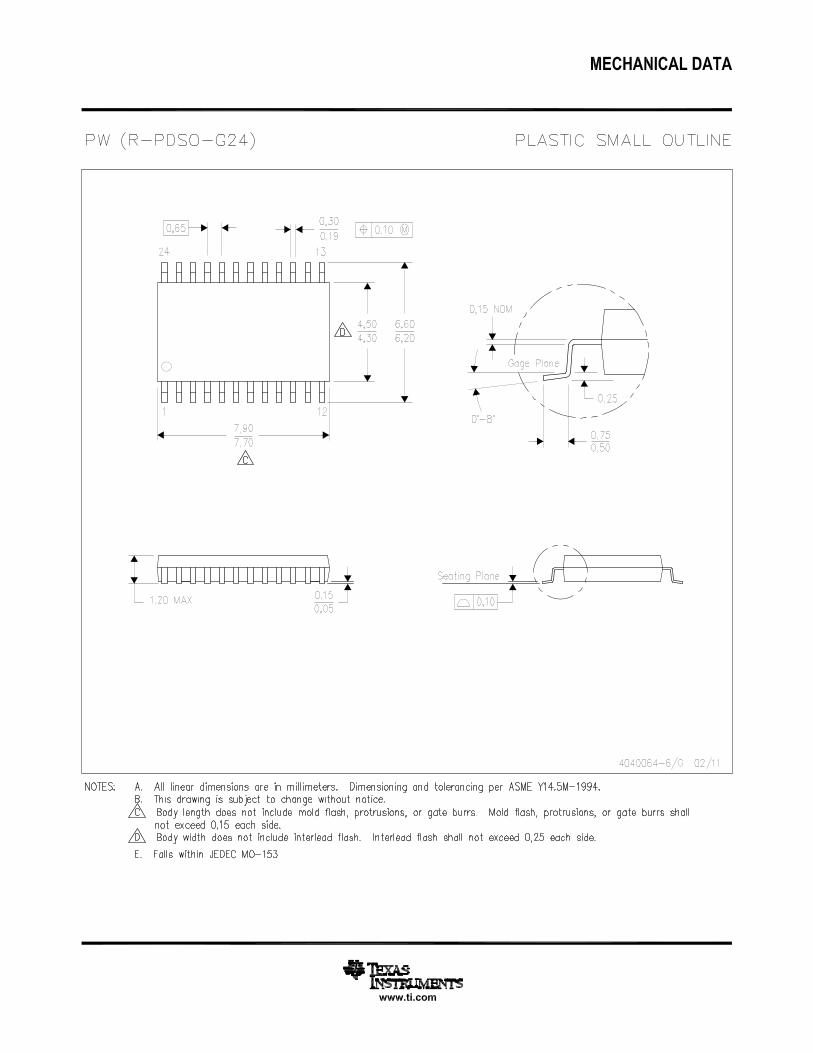
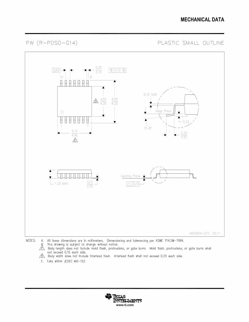
5 Pin Configuration and Functions
PW Package8-, 14-, 16-, 20, 24-Pin TSSOP
Top View
Pin FunctionsPIN
TYPE DESCRIPTIONNAME CDCLVC
1102CDCLVC
1103CDCLVC
1104CDCLVC
1106CDCLVC
1108CDCLVC
1110CDCLVC
1112LVCMOS CLOCK INPUTCLKIN 1 1 1 1 1 1 1 Input Input PinCLOCK OUTPUT ENABLE1G 2 2 2 2 2 2 2 Input Output EnableLVCMOS CLOCK OUTPUTY0 3 3 3 3 3 3 3
Output LVCMOS output. Unusedoutputs can be left floating.
Y1 8 8 8 14 16 20 24Y2 — 5 5 11 13 17 21Y3 — — 7 13 15 19 23Y4 — — — 6 6 6 6Y5 — — — 9 11 15 19Y6 — — — — 8 8 8Y7 — — — — 9 13 17Y8 — — — — — 12 16Y9 — — — — — 10 10Y10 — — — — — — 14Y11 — — — — — — 12SUPPLY VOLTAGE
VDD 6 6 65 5
55
Power 2.5-V or device supply9
9 138 10 14 1812 14 18 22
GROUND
4
CDCLVC1102, CDCLVC1103, CDCLVC1104CDCLVC1106, CDCLVC1108, CDCLVC1110, CDCLVC1112SCAS895B –MAY 2010–REVISED FEBRUARY 2017 www.ti.com
Product Folder Links: CDCLVC1102 CDCLVC1103 CDCLVC1104 CDCLVC1106 CDCLVC1108 CDCLVC1110CDCLVC1112
Submit Documentation Feedback Copyright © 2010–2017, Texas Instruments Incorporated
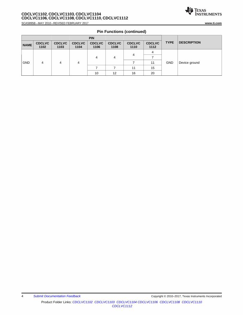
Pin Functions (continued)PIN
TYPE DESCRIPTIONNAME CDCLVC
1102CDCLVC
1103CDCLVC
1104CDCLVC
1106CDCLVC
1108CDCLVC
1110CDCLVC
1112
GND 4 4 44 4
44
GND Device ground7
7 117 7 11 1510 12 16 20
5
CDCLVC1102, CDCLVC1103, CDCLVC1104CDCLVC1106, CDCLVC1108, CDCLVC1110, CDCLVC1112
www.ti.com SCAS895B –MAY 2010–REVISED FEBRUARY 2017
Product Folder Links: CDCLVC1102 CDCLVC1103 CDCLVC1104 CDCLVC1106 CDCLVC1108 CDCLVC1110CDCLVC1112
Submit Documentation FeedbackCopyright © 2010–2017, Texas Instruments Incorporated
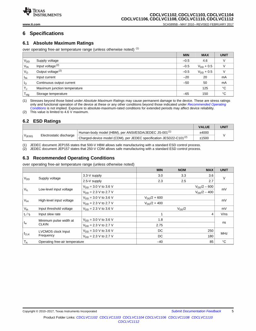
(1) Stresses beyond those listed under Absolute Maximum Ratings may cause permanent damage to the device. These are stress ratingsonly and functional operation of the device at these or any other conditions beyond those indicated under Recommended OperatingConditions is not implied. Exposure to absolute-maximum-rated conditions for extended periods may affect device reliability.
(2) This value is limited to 4.6 V maximum.
6 Specifications
6.1 Absolute Maximum Ratingsover operating free-air temperature range (unless otherwise noted) (1)
MIN MAX UNITVDD Supply voltage –0.5 4.6 VVIN Input voltage (2) –0.5 VDD + 0.5 VVO Output voltage (2) –0.5 VDD + 0.5 VIIN Input current –20 20 mAIO Continuous output current –50 50 mATJ Maximum junction temperature 125 °CTstg Storage temperature –65 150 °C
(1) JEDEC document JEP155 states that 500-V HBM allows safe manufacturing with a standard ESD control process.(2) JEDEC document JEP157 states that 250-V CDM allows safe manufacturing with a standard ESD control process.
6.2 ESD RatingsVALUE UNIT
V(ESD) Electrostatic dischargeHuman-body model (HBM), per ANSI/ESDA/JEDEC JS-001 (1) ±4000
VCharged-device model (CDM), per JEDEC specification JESD22-C101 (2) ±1500
6.3 Recommended Operating Conditionsover operating free-air temperature range (unless otherwise noted)
MIN NOM MAX UNIT
VDD Supply voltage3.3-V supply 3.0 3.3 3.6
V2.5-V supply 2.3 2.5 2.7
VIL Low-level input voltageVDD = 3.0 V to 3.6 V VDD/2 – 600
mVVDD = 2.3 V to 2.7 V VDD/2 – 400
VIH High-level input voltageVDD = 3.0 V to 3.6 V VDD/2 + 600
mVVDD = 2.3 V to 2.7 V VDD/2 + 400
Vth Input threshold voltage VDD = 2.3 V to 3.6 V VDD/2 mVtr / tf Input slew rate 1 4 V/ns
twMinimum pulse width atCLKIN
VDD = 3.0 V to 3.6 V 1.8ns
VDD = 2.3 V to 2.7 V 2.75
fCLKLVCMOS clock InputFrequency
VDD = 3.0 V to 3.6 V DC 250MHz
VDD = 2.3 V to 2.7 V DC 180TA Operating free-air temperature –40 85 °C
6
CDCLVC1102, CDCLVC1103, CDCLVC1104CDCLVC1106, CDCLVC1108, CDCLVC1110, CDCLVC1112SCAS895B –MAY 2010–REVISED FEBRUARY 2017 www.ti.com
Product Folder Links: CDCLVC1102 CDCLVC1103 CDCLVC1104 CDCLVC1106 CDCLVC1108 CDCLVC1110CDCLVC1112
Submit Documentation Feedback Copyright © 2010–2017, Texas Instruments Incorporated
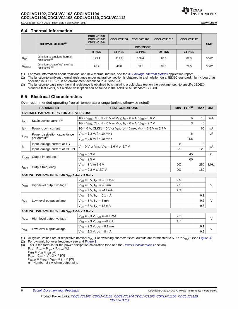
(1) For more information about traditional and new thermal metrics, see the IC Package Thermal Metrics application report.(2) The junction-to-ambient thermal resistance under natural convection is obtained in a simulation on a JEDEC-standard, high-K board, as
specified in JESD51-7, in an environment described in JESD51-2a.(3) The junction-to-case (top) thermal resistance is obtained by simulating a cold plate test on the package top. No specific JEDEC-
standard test exists, but a close description can be found in the ANSI SEMI standard G30-88.
6.4 Thermal Information
THERMAL METRIC (1)
CDCLVC1102CDCLVC1103CDCLVC1104
CDCLVC1106 CDCLVC1108 CDCLVC11010 CDCLVC1112
UNITPW (TSSOP)
8 PINS 14 PINS 16 PINS 20 PINS 24 PINS
RθJAJunction-to-ambient thermalresistance (2) 149.4 112.6 108.4 83.0 87.9 °C/W
RθJC(top)Junction-to-case(top) thermalresistance (3) 69.4 48.0 33.6 32.3 26.5 °C/W
(1) All typical values are at respective nominal VDD. For switching characteristics, outputs are terminated to 50 Ω to VDD/2 (see Figure 3).(2) For dynamic IDD over frequency see and Figure 1.(3) This is the formula for the power dissipation calculation (see and the Power Considerations section).
Ptot = Pstat + Pdyn + PCload [W]Pstat = VDD × IDD [W]Pdyn = CPD × VDD2 × ƒ [W]PCload = Cload × VDD2 × ƒ × n [W]n = Number of switching output pins
6.5 Electrical CharacteristicsOver recommended operating free-air temperature range (unless otherwise noted)
PARAMETER TEST CONDITIONS MIN TYP (1) MAX UNITOVERALL PARAMETERS FOR ALL VERSIONS
IDD Static device current (2) 1G = VDD; CLKIN = 0 V or VDD; IO = 0 mA; VDD = 3.6 V 6 10 mA1G = VDD; CLKIN = 0 V or VDD; IO = 0 mA; VDD = 2.7 V 3 6
IPD Power-down current 1G = 0 V; CLKIN = 0 V or VDD; IO = 0 mA; VDD = 3.6 V or 2.7 V 60 µA
CPDPower dissipation capacitanceper output (3)
VDD = 3.3 V; f = 10 MHz 6 pFVDD = 2.5 V; f = 10 MHz 4.5
IIInput leakage current at 1G
VI = 0 V or VDD, VDD = 3.6 V or 2.7 V8 8
µAInput leakage current at CLKIN 25 25
ROUT Output impedanceVDD = 3.3 V 45 Ω
VDD = 2.5 V 60
fOUT Output frequencyVDD = 3 V to 3.6 V DC 250 MHzVDD = 2.3 V to 2.7 V DC 180
OUTPUT PARAMETERS FOR VDD = 3.3 V ± 0.3 V
VOH High-level output voltageVDD = 3 V, IOH = –0.1 mA 2.9
VVDD = 3 V, IOH = –8 mA 2.5VDD = 3 V, IOH = –12 mA 2.2
VOL Low-level output voltageVDD = 3 V, IOL = 0.1 mA 0.1
VVDD = 3 V, IOL = 8 mA 0.5VDD = 3 V, IOL = 12 mA 0.8
OUTPUT PARAMETERS FOR VDD = 2.5 V ± 0.2 V
VOH High-level output voltageVDD = 2.3 V, IOH = –0.1 mA 2.2
VVDD = 2.3 V, IOH = –8 mA 1.7
VOL Low-level output voltageVDD = 2.3 V, IOL = 0.1 mA 0.1
VVDD = 2.3 V, IOL = 8 mA 0.5
0
1
2
3
0 20 40 60 80 100 120 140 160 180
I = C * V * fdyn PD DD
V = 2.5 VDD
f - Clock Frequency - MHz
I-
Dy
na
mic
Su
pp
ly C
urr
en
t -
mA
dy
n
0
5
10
15
0 20 40 60 80 100 120 140 160 180
V = 2.5 VDD P + Pdyn Cload8pF
P + Pdyn Cload50/2
P + Pdyn Cload2pF
f - Clock Frequency - MHz
De
vic
e P
ow
er
Co
ns
um
pti
on
- m
W
7
CDCLVC1102, CDCLVC1103, CDCLVC1104CDCLVC1106, CDCLVC1108, CDCLVC1110, CDCLVC1112
www.ti.com SCAS895B –MAY 2010–REVISED FEBRUARY 2017
Product Folder Links: CDCLVC1102 CDCLVC1103 CDCLVC1104 CDCLVC1106 CDCLVC1108 CDCLVC1110CDCLVC1112
Submit Documentation FeedbackCopyright © 2010–2017, Texas Instruments Incorporated
(1) tsk(p) depends on output rise- and fall-time (tr/tf). The output duty-cycle can be calculated: odc = (tw(OUT) ± tsk(p))/tperiod; tw(OUT) is pulse-width of output waveform and tperiod is 1/fOUT.
(2) Parameter is specified by characterization. Not tested in production.
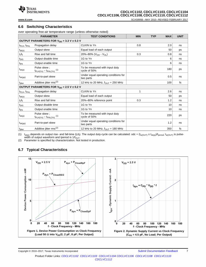
6.6 Switching Characteristicsover operating free-air temperature range (unless otherwise noted)
PARAMETER TEST CONDITIONS MIN TYP MAX UNITOUTPUT PARAMETERS FOR VDD = 3.3 V ± 0.3 VtPLH, tPHL Propagation delay CLKIN to Yn 0.8 2.0 nstsk(o) Output skew Equal load of each output 50 pstr/tf Rise and fall time 20%–80% (VOH - VOL) 0.3 0.8 nstDIS Output disable time 1G to Yn 6 nstEN Output enable time 1G to Yn 6 ns
tsk(p)Pulse skew ;tPLH(Yn) – tPHL(Yn)
(1)To be measured with input dutycycle of 50% 180 ps
tsk(pp) Part-to-part skew Under equal operating conditions fortwo parts 0.5 ns
tjitter Additive jitter rms (2) 12 kHz to 20 MHz, fOUT = 250 MHz 100 fsOUTPUT PARAMETERS FOR VDD = 2.5 V ± 0.2 VtPLH, tPHL Propagation delay CLKIN to Yn 1 2.6 nstsk(o) Output skew Equal load of each output 50 pstr/tf Rise and fall time 20%–80% reference point 0.3 1.2 nstDIS Output disable time 1G to Yn 10 nstEN Output enable time 1G to Yn 10 ns
tsk(p)Pulse skew ;tPLH(Yn) – tPHL(Yn)
(1)To be measured with input dutycycle of 50% 220 ps
tsk(pp) Part-to-part skew Under equal operating conditions fortwo parts 1.2 ns
tjitter Additive jitter rms (2) 12 kHz to 20 MHz, fOUT = 180 MHz 350 fs
6.7 Typical Characteristics
Figure 1. Device Power Consumption vs Clock Frequency(Load 50 Ω into VDD/2; 2 pF, 8 pF; Per Output)
Figure 2. Dynamic Supply Current vs Clock Frequency(CPD = 4.5 pF, No Load; Per Output)
tsk(o)
VDD / 2
Yn+1
VDD / 2
Yn
tsk(o)tDIS tEN
VIN / 2
1 G
Yn
VIN / 2
LVCMOSOutput Z = 50O W
RS = 10 (V = 3.3 V)
RS = 0 (V = 2.5 V)
W
W
DD
DD
parasitic input capacitance
V = 3.3 V or 2.5 VDD
LVCMOSOutput
VDD
R=100 W
R= 100 W
Z = 50O W
parasitic input capacitance
V = 3.3 V or 2.5 VDD
Z = 50O W
R=50 W
from Measurement Equipment
V /2DD
LVCMOSOutput
V = 3.3 V or 2.5 VDD
C = 2 pF
parasitic capasitance
8
CDCLVC1102, CDCLVC1103, CDCLVC1104CDCLVC1106, CDCLVC1108, CDCLVC1110, CDCLVC1112SCAS895B –MAY 2010–REVISED FEBRUARY 2017 www.ti.com
Product Folder Links: CDCLVC1102 CDCLVC1103 CDCLVC1104 CDCLVC1106 CDCLVC1108 CDCLVC1110CDCLVC1112
Submit Documentation Feedback Copyright © 2010–2017, Texas Instruments Incorporated
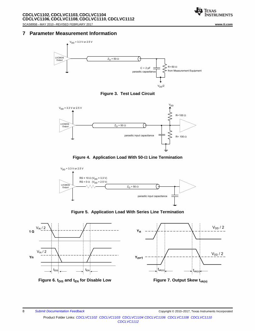
7 Parameter Measurement Information
Figure 3. Test Load Circuit
Figure 4. Application Load With 50-Ω Line Termination
Figure 5. Application Load With Series Line Termination
Figure 6. tDIS and tEN for Disable Low Figure 7. Output Skew tsk(o)

tPLH
V DD/ 2
Yn
V DD/ 2
CLKIN
tPHL
Note: tsk (p) = | tPLH – t PHL |
tr
Yn
80 % V OH -V OL
CLKIN
tf
20 % V OH -V OL
VOH
V OL
9
CDCLVC1102, CDCLVC1103, CDCLVC1104CDCLVC1106, CDCLVC1108, CDCLVC1110, CDCLVC1112
www.ti.com SCAS895B –MAY 2010–REVISED FEBRUARY 2017
Product Folder Links: CDCLVC1102 CDCLVC1103 CDCLVC1104 CDCLVC1106 CDCLVC1108 CDCLVC1110CDCLVC1112
Submit Documentation FeedbackCopyright © 2010–2017, Texas Instruments Incorporated
Parameter Measurement Information (continued)
Figure 8. Pulse Skew tsk(p) and Propagation DelaytPLH/tPHL
Figure 9. Rise/Fall Times tr/tf
CDCLVC 1112
1
1G 2
GND
3
CLKIN
4
5
6
7
8
9
10
16
17
18
19
20
21
22
23
24 Y1
Y2
VDD
VDD
Y3
Y4
VDD
GND
Y0
Y11
Y5
GND
Y6 Y7
Y9
VDD Y8
GND
11
12 13
14
15
GND Y10
VDD
CDCLVC 1106
CDCLVC 1110
CDCLVC 1102
CDCLVC 1103
CDCLVC 1104
CDCLVC 1108
Y0
Y1
Y2
Y3
Yn
CLKINLV
CMOS
1G
LVCMOS
LVCMOS
LVCMOS
LVCMOS
LV
CMOS
•
•
•
10
CDCLVC1102, CDCLVC1103, CDCLVC1104CDCLVC1106, CDCLVC1108, CDCLVC1110, CDCLVC1112SCAS895B –MAY 2010–REVISED FEBRUARY 2017 www.ti.com
Product Folder Links: CDCLVC1102 CDCLVC1103 CDCLVC1104 CDCLVC1106 CDCLVC1108 CDCLVC1110CDCLVC1112
Submit Documentation Feedback Copyright © 2010–2017, Texas Instruments Incorporated
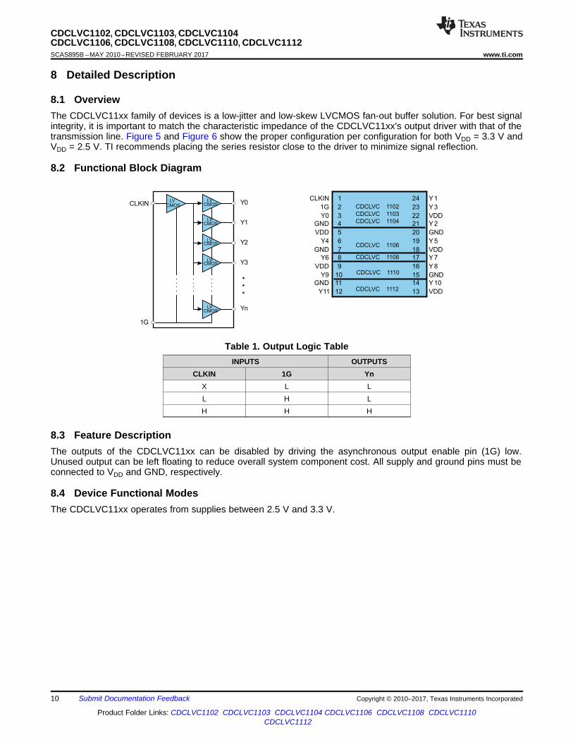
8 Detailed Description
8.1 OverviewThe CDCLVC11xx family of devices is a low-jitter and low-skew LVCMOS fan-out buffer solution. For best signalintegrity, it is important to match the characteristic impedance of the CDCLVC11xx's output driver with that of thetransmission line. Figure 5 and Figure 6 show the proper configuration per configuration for both VDD = 3.3 V andVDD = 2.5 V. TI recommends placing the series resistor close to the driver to minimize signal reflection.
8.2 Functional Block Diagram
Table 1. Output Logic TableINPUTS OUTPUTS
CLKIN 1G YnX L LL H LH H H
8.3 Feature DescriptionThe outputs of the CDCLVC11xx can be disabled by driving the asynchronous output enable pin (1G) low.Unused output can be left floating to reduce overall system component cost. All supply and ground pins must beconnected to VDD and GND, respectively.
8.4 Device Functional ModesThe CDCLVC11xx operates from supplies between 2.5 V and 3.3 V.
11
CDCLVC1102, CDCLVC1103, CDCLVC1104CDCLVC1106, CDCLVC1108, CDCLVC1110, CDCLVC1112
www.ti.com SCAS895B –MAY 2010–REVISED FEBRUARY 2017
Product Folder Links: CDCLVC1102 CDCLVC1103 CDCLVC1104 CDCLVC1106 CDCLVC1108 CDCLVC1110CDCLVC1112
Submit Documentation FeedbackCopyright © 2010–2017, Texas Instruments Incorporated
9 Application and Implementation
NOTEInformation in the following applications sections is not part of the TI componentspecification, and TI does not warrant its accuracy or completeness. TI’s customers areresponsible for determining suitability of components for their purposes. Customers shouldvalidate and test their design implementation to confirm system functionality.
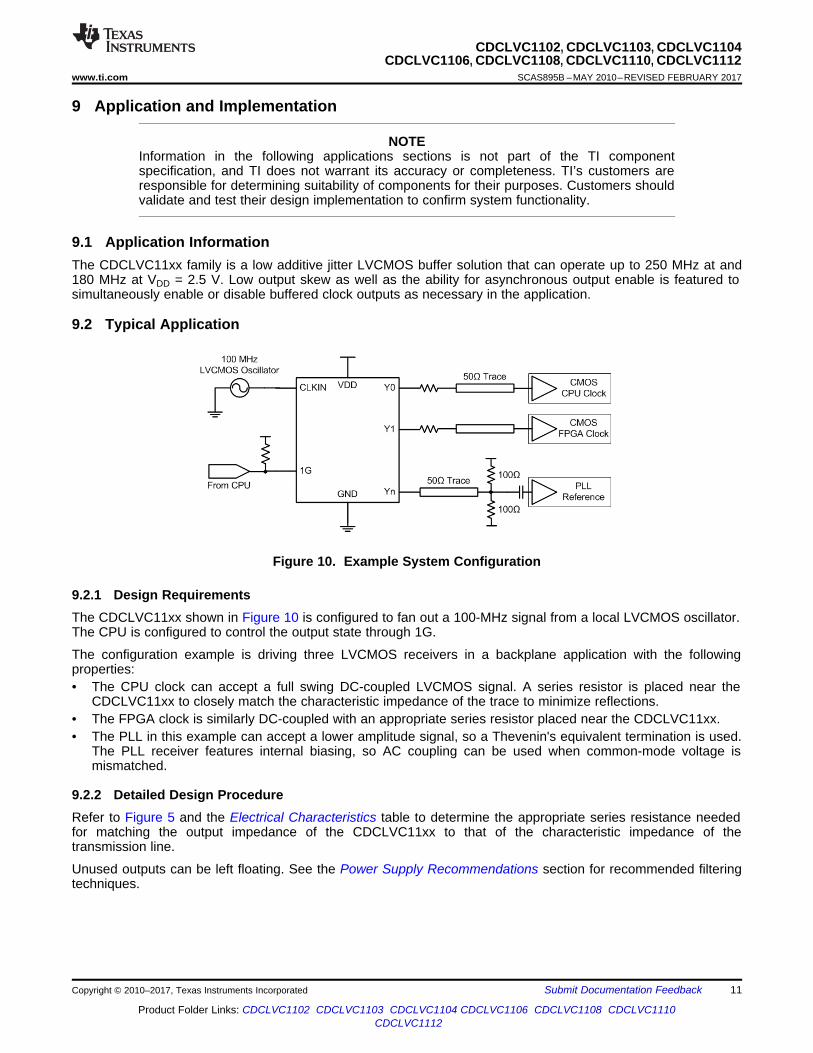
9.1 Application InformationThe CDCLVC11xx family is a low additive jitter LVCMOS buffer solution that can operate up to 250 MHz at and180 MHz at VDD = 2.5 V. Low output skew as well as the ability for asynchronous output enable is featured tosimultaneously enable or disable buffered clock outputs as necessary in the application.
9.2 Typical Application
Figure 10. Example System Configuration
9.2.1 Design RequirementsThe CDCLVC11xx shown in Figure 10 is configured to fan out a 100-MHz signal from a local LVCMOS oscillator.The CPU is configured to control the output state through 1G.
The configuration example is driving three LVCMOS receivers in a backplane application with the followingproperties:• The CPU clock can accept a full swing DC-coupled LVCMOS signal. A series resistor is placed near the
CDCLVC11xx to closely match the characteristic impedance of the trace to minimize reflections.• The FPGA clock is similarly DC-coupled with an appropriate series resistor placed near the CDCLVC11xx.• The PLL in this example can accept a lower amplitude signal, so a Thevenin's equivalent termination is used.
The PLL receiver features internal biasing, so AC coupling can be used when common-mode voltage ismismatched.
9.2.2 Detailed Design ProcedureRefer to Figure 5 and the Electrical Characteristics table to determine the appropriate series resistance neededfor matching the output impedance of the CDCLVC11xx to that of the characteristic impedance of thetransmission line.
Unused outputs can be left floating. See the Power Supply Recommendations section for recommended filteringtechniques.

12
CDCLVC1102, CDCLVC1103, CDCLVC1104CDCLVC1106, CDCLVC1108, CDCLVC1110, CDCLVC1112SCAS895B –MAY 2010–REVISED FEBRUARY 2017 www.ti.com
Product Folder Links: CDCLVC1102 CDCLVC1103 CDCLVC1104 CDCLVC1106 CDCLVC1108 CDCLVC1110CDCLVC1112
Submit Documentation Feedback Copyright © 2010–2017, Texas Instruments Incorporated
Typical Application (continued)9.2.3 Application Curves
Figure 11. CDCLVC11xx Reference Phase Noise 26 fs(12 kHz to 20 MHz)
Figure 12. CDCLVC11xx Output Phase Noise 86 fs(12 kHz to 20 MHz)
The low additive jitter of the CDCLVC11xx can be shown in the previous application example. The low-noise100-MHz XO with 26-fs RMS jitter drives the CDCLVC11xx, resulting in 86-fs RMS jitter when integrated from 12kHz to 20 MHz. The resultant additive jitter is a low 82-fs RMS for this configuration.
10 Power Supply Recommendations
High-performance clock buffers are sensitive to noise on the power supply, which can dramatically increase theadditive jitter of the buffer. Thus, it is essential to reduce noise from the system power supply, especially whenthe jitter and phase noise is critical to applications.
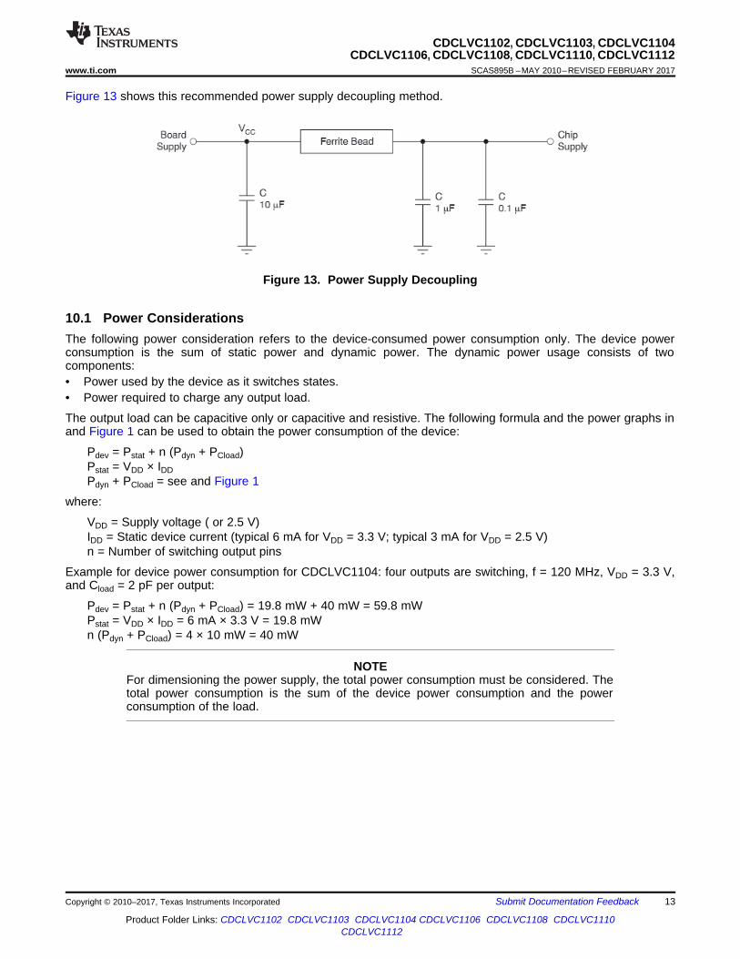
Filter capacitors are used to eliminate the low-frequency noise from the power supply, where the bypasscapacitors provide the very low impedance path for high-frequency noise and guards the power supply systemagainst induced fluctuations. These bypass capacitors also provide instantaneous current surges as required bythe device and should have low equivalent series resistance (ESR). To properly use the bypass capacitors, theymust be placed very close to the power-supply terminals and laid out with short loops to minimize inductance. TIrecommends adding as many high-frequency (for example, 0.1 µF) bypass capacitors, as there are supplyterminals in the package. TI recommends, but does not require, inserting a ferrite bead between the board powersupply and the chip power supply that isolates the high-frequency switching noises generated by the clock buffer;these beads prevent the switching noise from leaking into the board supply. It is imperative to choose anappropriate ferrite bead with very low DC resistance to provide adequate isolation between the board supply andthe chip supply, as well as to maintain a voltage at the supply terminals that is greater than the minimum voltagerequired for proper operation.
13
CDCLVC1102, CDCLVC1103, CDCLVC1104CDCLVC1106, CDCLVC1108, CDCLVC1110, CDCLVC1112
www.ti.com SCAS895B –MAY 2010–REVISED FEBRUARY 2017
Product Folder Links: CDCLVC1102 CDCLVC1103 CDCLVC1104 CDCLVC1106 CDCLVC1108 CDCLVC1110CDCLVC1112
Submit Documentation FeedbackCopyright © 2010–2017, Texas Instruments Incorporated
Figure 13 shows this recommended power supply decoupling method.
Figure 13. Power Supply Decoupling
10.1 Power ConsiderationsThe following power consideration refers to the device-consumed power consumption only. The device powerconsumption is the sum of static power and dynamic power. The dynamic power usage consists of twocomponents:• Power used by the device as it switches states.• Power required to charge any output load.
The output load can be capacitive only or capacitive and resistive. The following formula and the power graphs inand Figure 1 can be used to obtain the power consumption of the device:
Pdev = Pstat + n (Pdyn + PCload)Pstat = VDD × IDDPdyn + PCload = see and Figure 1
where:
VDD = Supply voltage ( or 2.5 V)IDD = Static device current (typical 6 mA for VDD = 3.3 V; typical 3 mA for VDD = 2.5 V)n = Number of switching output pins
Example for device power consumption for CDCLVC1104: four outputs are switching, f = 120 MHz, VDD = 3.3 V,and Cload = 2 pF per output:
Pdev = Pstat + n (Pdyn + PCload) = 19.8 mW + 40 mW = 59.8 mWPstat = VDD × IDD = 6 mA × 3.3 V = 19.8 mWn (Pdyn + PCload) = 4 × 10 mW = 40 mW
NOTEFor dimensioning the power supply, the total power consumption must be considered. Thetotal power consumption is the sum of the device power consumption and the powerconsumption of the load.

14
CDCLVC1102, CDCLVC1103, CDCLVC1104CDCLVC1106, CDCLVC1108, CDCLVC1110, CDCLVC1112SCAS895B –MAY 2010–REVISED FEBRUARY 2017 www.ti.com
Product Folder Links: CDCLVC1102 CDCLVC1103 CDCLVC1104 CDCLVC1106 CDCLVC1108 CDCLVC1110CDCLVC1112
Submit Documentation Feedback Copyright © 2010–2017, Texas Instruments Incorporated
11 Layout
11.1 Layout GuidelinesFigure 14 shows a conceptual layout detailing recommended placement of power supply bypass capacitors. Forcomponent side mounting, use 0402 body size capacitors to facilitate signal routing. Keep the connectionsbetween the bypass capacitors and the power supply on the device as short as possible. Ground the other sideof the capacitor using a low-impedance connection to the ground plane.
11.2 Layout Example
Figure 14. PCB Conceptual Layout
15
CDCLVC1102, CDCLVC1103, CDCLVC1104CDCLVC1106, CDCLVC1108, CDCLVC1110, CDCLVC1112
www.ti.com SCAS895B –MAY 2010–REVISED FEBRUARY 2017
Product Folder Links: CDCLVC1102 CDCLVC1103 CDCLVC1104 CDCLVC1106 CDCLVC1108 CDCLVC1110CDCLVC1112
Submit Documentation FeedbackCopyright © 2010–2017, Texas Instruments Incorporated
12 Device and Documentation Support
12.1 Related LinksThe table below lists quick access links. Categories include technical documents, support and communityresources, tools and software, and quick access to sample or buy.
Table 2. Related Links
PARTS PRODUCT FOLDER SAMPLE & BUY TECHNICALDOCUMENTS
TOOLS &SOFTWARE
SUPPORT &COMMUNITY
CDCLVC1102 Click here Click here Click here Click here Click hereCDCLVC1103 Click here Click here Click here Click here Click hereCDCLVC1104 Click here Click here Click here Click here Click hereCDCLVC1106 Click here Click here Click here Click here Click hereCDCLVC1108 Click here Click here Click here Click here Click hereCDCLVC1110 Click here Click here Click here Click here Click hereCDCLVC1112 Click here Click here Click here Click here Click here
12.2 Receiving Notification of Documentation UpdatesTo receive notification of documentation updates, navigate to the device product folder on ti.com. In the upperright corner, click on Alert me to register and receive a weekly digest of any product information that haschanged. For change details, review the revision history included in any revised document.
12.3 Community ResourcesThe following links connect to TI community resources. Linked contents are provided "AS IS" by the respectivecontributors. They do not constitute TI specifications and do not necessarily reflect TI's views; see TI's Terms ofUse.
TI E2E™ Online Community TI's Engineer-to-Engineer (E2E) Community. Created to foster collaborationamong engineers. At e2e.ti.com, you can ask questions, share knowledge, explore ideas and helpsolve problems with fellow engineers.
Design Support TI's Design Support Quickly find helpful E2E forums along with design support tools andcontact information for technical support.
12.4 TrademarksE2E is a trademark of Texas Instruments.All other trademarks are the property of their respective owners.
12.5 Electrostatic Discharge CautionThese devices have limited built-in ESD protection. The leads should be shorted together or the device placed in conductive foamduring storage or handling to prevent electrostatic damage to the MOS gates.
12.6 GlossarySLYZ022 — TI Glossary.
This glossary lists and explains terms, acronyms, and definitions.
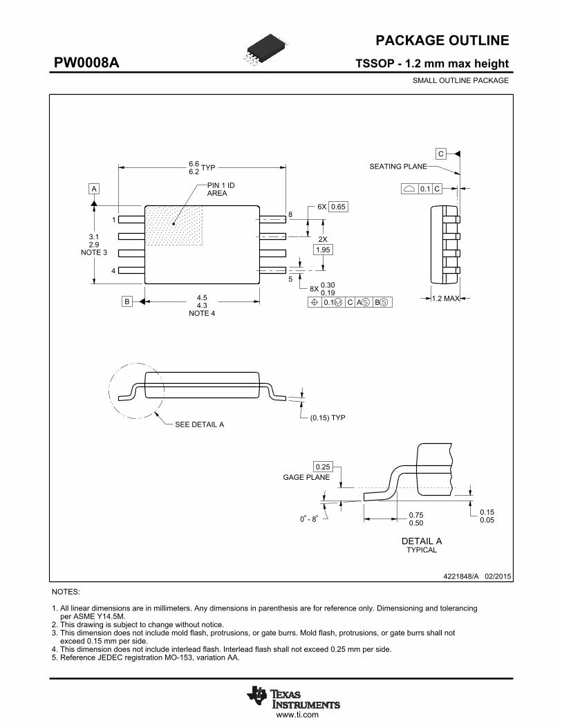
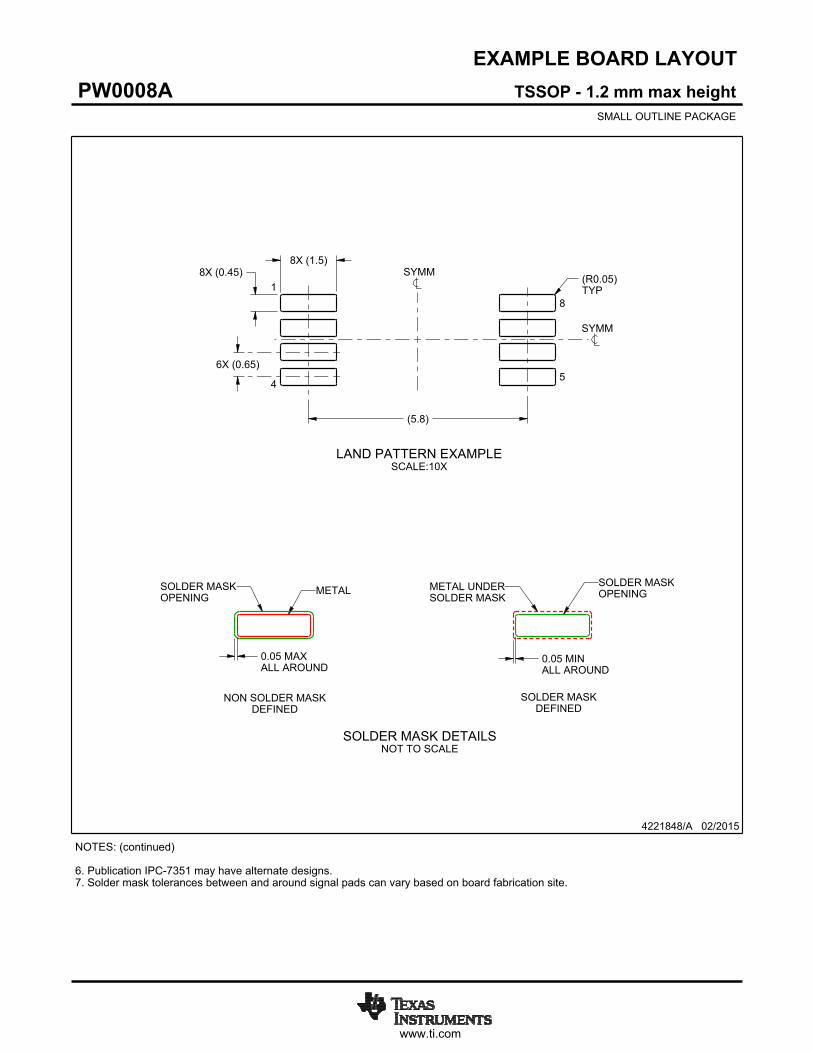
13 Mechanical, Packaging, and Orderable InformationThe following pages include mechanical, packaging, and orderable information. This information is the mostcurrent data available for the designated devices. This data is subject to change without notice and revision ofthis document. For browser-based versions of this data sheet, refer to the left-hand navigation.
PACKAGE OPTION ADDENDUM
www.ti.com 8-Oct-2015
Addendum-Page 1
PACKAGING INFORMATION
Orderable Device Status(1)
Package Type PackageDrawing
Pins PackageQty
Eco Plan(2)
Lead/Ball Finish(6)
MSL Peak Temp(3)
Op Temp (°C) Device Marking(4/5)
Samples
CDCLVC1102PW ACTIVE TSSOP PW 8 150 Green (RoHS& no Sb/Br)
CU NIPDAU Level-1-260C-UNLIM -40 to 85 C9C2
CDCLVC1102PWR ACTIVE TSSOP PW 8 2000 Green (RoHS& no Sb/Br)
CU NIPDAU Level-1-260C-UNLIM -40 to 85 C9C2
CDCLVC1103PW ACTIVE TSSOP PW 8 150 Green (RoHS& no Sb/Br)
CU NIPDAU Level-1-260C-UNLIM -40 to 85 C9C3
CDCLVC1103PWR ACTIVE TSSOP PW 8 2000 Green (RoHS& no Sb/Br)
CU NIPDAU Level-1-260C-UNLIM -40 to 85 C9C3
CDCLVC1104PW ACTIVE TSSOP PW 8 150 Green (RoHS& no Sb/Br)
CU NIPDAU Level-1-260C-UNLIM -40 to 85 C9C4
CDCLVC1104PWR ACTIVE TSSOP PW 8 2000 Green (RoHS& no Sb/Br)
CU NIPDAU Level-1-260C-UNLIM -40 to 85 C9C4
CDCLVC1106PW ACTIVE TSSOP PW 14 90 Green (RoHS& no Sb/Br)
CU NIPDAU Level-1-260C-UNLIM -40 to 85 C9C6
CDCLVC1106PWR ACTIVE TSSOP PW 14 2000 Green (RoHS& no Sb/Br)
CU NIPDAU Level-1-260C-UNLIM -40 to 85 C9C6
CDCLVC1108PW ACTIVE TSSOP PW 16 90 Green (RoHS& no Sb/Br)
CU NIPDAU Level-1-260C-UNLIM -40 to 85 C9C8
CDCLVC1108PWR ACTIVE TSSOP PW 16 2000 Green (RoHS& no Sb/Br)
CU NIPDAU Level-1-260C-UNLIM -40 to 85 C9C8
CDCLVC1110PW ACTIVE TSSOP PW 20 70 Green (RoHS& no Sb/Br)
CU NIPDAU Level-1-260C-UNLIM -40 to 85 C9CA
CDCLVC1110PWR ACTIVE TSSOP PW 20 2000 Green (RoHS& no Sb/Br)
CU NIPDAU Level-1-260C-UNLIM -40 to 85 C9CA
CDCLVC1112PW ACTIVE TSSOP PW 24 60 Green (RoHS& no Sb/Br)
CU NIPDAU Level-1-260C-UNLIM -40 to 85 C9CC
CDCLVC1112PWR ACTIVE TSSOP PW 24 2000 Green (RoHS& no Sb/Br)
CU NIPDAU Level-1-260C-UNLIM -40 to 85 C9CC
(1) The marketing status values are defined as follows:ACTIVE: Product device recommended for new designs.LIFEBUY: TI has announced that the device will be discontinued, and a lifetime-buy period is in effect.NRND: Not recommended for new designs. Device is in production to support existing customers, but TI does not recommend using this part in a new design.PREVIEW: Device has been announced but is not in production. Samples may or may not be available.OBSOLETE: TI has discontinued the production of the device.
PACKAGE OPTION ADDENDUM
www.ti.com 8-Oct-2015
Addendum-Page 2
(2) Eco Plan - The planned eco-friendly classification: Pb-Free (RoHS), Pb-Free (RoHS Exempt), or Green (RoHS & no Sb/Br) - please check http://www.ti.com/productcontent for the latest availabilityinformation and additional product content details.TBD: The Pb-Free/Green conversion plan has not been defined.Pb-Free (RoHS): TI's terms "Lead-Free" or "Pb-Free" mean semiconductor products that are compatible with the current RoHS requirements for all 6 substances, including the requirement thatlead not exceed 0.1% by weight in homogeneous materials. Where designed to be soldered at high temperatures, TI Pb-Free products are suitable for use in specified lead-free processes.Pb-Free (RoHS Exempt): This component has a RoHS exemption for either 1) lead-based flip-chip solder bumps used between the die and package, or 2) lead-based die adhesive used betweenthe die and leadframe. The component is otherwise considered Pb-Free (RoHS compatible) as defined above.Green (RoHS & no Sb/Br): TI defines "Green" to mean Pb-Free (RoHS compatible), and free of Bromine (Br) and Antimony (Sb) based flame retardants (Br or Sb do not exceed 0.1% by weightin homogeneous material)
(3) MSL, Peak Temp. - The Moisture Sensitivity Level rating according to the JEDEC industry standard classifications, and peak solder temperature.
(4) There may be additional marking, which relates to the logo, the lot trace code information, or the environmental category on the device.
(5) Multiple Device Markings will be inside parentheses. Only one Device Marking contained in parentheses and separated by a "~" will appear on a device. If a line is indented then it is a continuationof the previous line and the two combined represent the entire Device Marking for that device.
(6) Lead/Ball Finish - Orderable Devices may have multiple material finish options. Finish options are separated by a vertical ruled line. Lead/Ball Finish values may wrap to two lines if the finishvalue exceeds the maximum column width.
Important Information and Disclaimer:The information provided on this page represents TI's knowledge and belief as of the date that it is provided. TI bases its knowledge and belief on informationprovided by third parties, and makes no representation or warranty as to the accuracy of such information. Efforts are underway to better integrate information from third parties. TI has taken andcontinues to take reasonable steps to provide representative and accurate information but may not have conducted destructive testing or chemical analysis on incoming materials and chemicals.TI and TI suppliers consider certain information to be proprietary, and thus CAS numbers and other limited information may not be available for release.
In no event shall TI's liability arising out of such information exceed the total purchase price of the TI part(s) at issue in this document sold by TI to Customer on an annual basis.
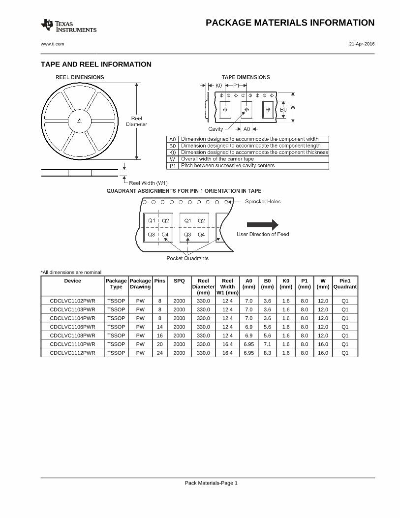
TAPE AND REEL INFORMATION
*All dimensions are nominal
Device PackageType
PackageDrawing
Pins SPQ ReelDiameter
(mm)
ReelWidth
W1 (mm)
A0(mm)
B0(mm)
K0(mm)
P1(mm)
W(mm)
Pin1Quadrant
CDCLVC1102PWR TSSOP PW 8 2000 330.0 12.4 7.0 3.6 1.6 8.0 12.0 Q1
CDCLVC1103PWR TSSOP PW 8 2000 330.0 12.4 7.0 3.6 1.6 8.0 12.0 Q1
CDCLVC1104PWR TSSOP PW 8 2000 330.0 12.4 7.0 3.6 1.6 8.0 12.0 Q1
CDCLVC1106PWR TSSOP PW 14 2000 330.0 12.4 6.9 5.6 1.6 8.0 12.0 Q1
CDCLVC1108PWR TSSOP PW 16 2000 330.0 12.4 6.9 5.6 1.6 8.0 12.0 Q1
CDCLVC1110PWR TSSOP PW 20 2000 330.0 16.4 6.95 7.1 1.6 8.0 16.0 Q1
CDCLVC1112PWR TSSOP PW 24 2000 330.0 16.4 6.95 8.3 1.6 8.0 16.0 Q1
PACKAGE MATERIALS INFORMATION
www.ti.com 21-Apr-2016
Pack Materials-Page 1
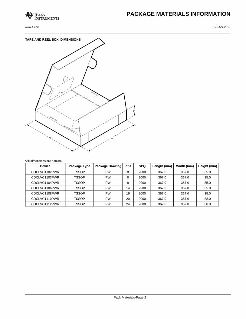
*All dimensions are nominal
Device Package Type Package Drawing Pins SPQ Length (mm) Width (mm) Height (mm)
CDCLVC1102PWR TSSOP PW 8 2000 367.0 367.0 35.0
CDCLVC1103PWR TSSOP PW 8 2000 367.0 367.0 35.0
CDCLVC1104PWR TSSOP PW 8 2000 367.0 367.0 35.0
CDCLVC1106PWR TSSOP PW 14 2000 367.0 367.0 35.0
CDCLVC1108PWR TSSOP PW 16 2000 367.0 367.0 35.0
CDCLVC1110PWR TSSOP PW 20 2000 367.0 367.0 38.0
CDCLVC1112PWR TSSOP PW 24 2000 367.0 367.0 38.0
PACKAGE MATERIALS INFORMATION
www.ti.com 21-Apr-2016
Pack Materials-Page 2


www.ti.com
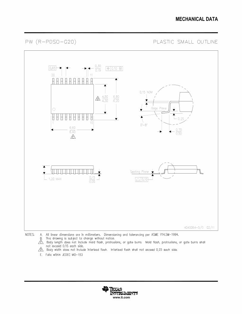
PACKAGE OUTLINE
C
TYP6.66.2
1.2 MAX
6X 0.65
8X 0.300.19
2X1.95
0.150.05
(0.15) TYP
0 - 8
0.25GAGE PLANE
0.750.50
A
NOTE 3
3.12.9
BNOTE 4
4.54.3
4221848/A 02/2015
TSSOP - 1.2 mm max heightPW0008ASMALL OUTLINE PACKAGE
NOTES: 1. All linear dimensions are in millimeters. Any dimensions in parenthesis are for reference only. Dimensioning and tolerancing per ASME Y14.5M. 2. This drawing is subject to change without notice. 3. This dimension does not include mold flash, protrusions, or gate burrs. Mold flash, protrusions, or gate burrs shall not exceed 0.15 mm per side. 4. This dimension does not include interlead flash. Interlead flash shall not exceed 0.25 mm per side.5. Reference JEDEC registration MO-153, variation AA.
18
0.1 C A B
54
PIN 1 IDAREA
SEATING PLANE
0.1 C
SEE DETAIL A
DETAIL ATYPICAL
SCALE 2.800
www.ti.com
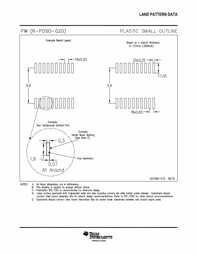
EXAMPLE BOARD LAYOUT
(5.8)
0.05 MAXALL AROUND
0.05 MINALL AROUND
8X (1.5)8X (0.45)
6X (0.65)
(R )TYP
0.05
4221848/A 02/2015
TSSOP - 1.2 mm max heightPW0008ASMALL OUTLINE PACKAGE
SYMM
SYMM
LAND PATTERN EXAMPLESCALE:10X
1
45
8
NOTES: (continued) 6. Publication IPC-7351 may have alternate designs. 7. Solder mask tolerances between and around signal pads can vary based on board fabrication site.
METALSOLDER MASKOPENING
NON SOLDER MASKDEFINED
SOLDER MASK DETAILSNOT TO SCALE
SOLDER MASKOPENING
METAL UNDERSOLDER MASK
SOLDER MASKDEFINED
www.ti.com
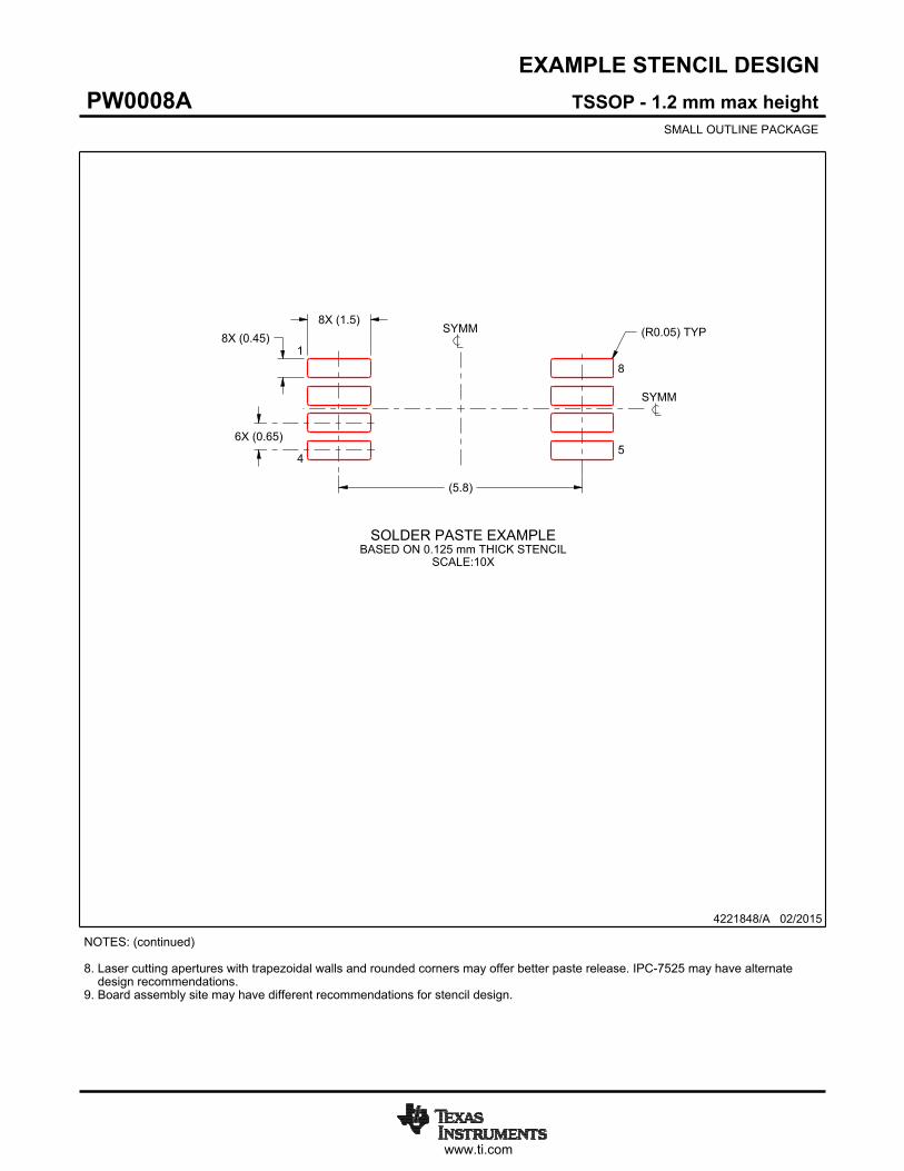
EXAMPLE STENCIL DESIGN
(5.8)
6X (0.65)
8X (0.45)8X (1.5)
(R ) TYP0.05
4221848/A 02/2015
TSSOP - 1.2 mm max heightPW0008ASMALL OUTLINE PACKAGE
NOTES: (continued) 8. Laser cutting apertures with trapezoidal walls and rounded corners may offer better paste release. IPC-7525 may have alternate design recommendations. 9. Board assembly site may have different recommendations for stencil design.
SYMM
SYMM
1
45
8
SOLDER PASTE EXAMPLEBASED ON 0.125 mm THICK STENCIL
SCALE:10X
IMPORTANT NOTICE
Texas Instruments Incorporated (TI) reserves the right to make corrections, enhancements, improvements and other changes to itssemiconductor products and services per JESD46, latest issue, and to discontinue any product or service per JESD48, latest issue. Buyersshould obtain the latest relevant information before placing orders and should verify that such information is current and complete.TI’s published terms of sale for semiconductor products (http://www.ti.com/sc/docs/stdterms.htm) apply to the sale of packaged integratedcircuit products that TI has qualified and released to market. Additional terms may apply to the use or sale of other types of TI products andservices.Reproduction of significant portions of TI information in TI data sheets is permissible only if reproduction is without alteration and isaccompanied by all associated warranties, conditions, limitations, and notices. TI is not responsible or liable for such reproduceddocumentation. Information of third parties may be subject to additional restrictions. Resale of TI products or services with statementsdifferent from or beyond the parameters stated by TI for that product or service voids all express and any implied warranties for theassociated TI product or service and is an unfair and deceptive business practice. TI is not responsible or liable for any such statements.Buyers and others who are developing systems that incorporate TI products (collectively, “Designers”) understand and agree that Designersremain responsible for using their independent analysis, evaluation and judgment in designing their applications and that Designers havefull and exclusive responsibility to assure the safety of Designers' applications and compliance of their applications (and of all TI productsused in or for Designers’ applications) with all applicable regulations, laws and other applicable requirements. Designer represents that, withrespect to their applications, Designer has all the necessary expertise to create and implement safeguards that (1) anticipate dangerousconsequences of failures, (2) monitor failures and their consequences, and (3) lessen the likelihood of failures that might cause harm andtake appropriate actions. Designer agrees that prior to using or distributing any applications that include TI products, Designer willthoroughly test such applications and the functionality of such TI products as used in such applications.TI’s provision of technical, application or other design advice, quality characterization, reliability data or other services or information,including, but not limited to, reference designs and materials relating to evaluation modules, (collectively, “TI Resources”) are intended toassist designers who are developing applications that incorporate TI products; by downloading, accessing or using TI Resources in anyway, Designer (individually or, if Designer is acting on behalf of a company, Designer’s company) agrees to use any particular TI Resourcesolely for this purpose and subject to the terms of this Notice.TI’s provision of TI Resources does not expand or otherwise alter TI’s applicable published warranties or warranty disclaimers for TIproducts, and no additional obligations or liabilities arise from TI providing such TI Resources. TI reserves the right to make corrections,enhancements, improvements and other changes to its TI Resources. TI has not conducted any testing other than that specificallydescribed in the published documentation for a particular TI Resource.Designer is authorized to use, copy and modify any individual TI Resource only in connection with the development of applications thatinclude the TI product(s) identified in such TI Resource. NO OTHER LICENSE, EXPRESS OR IMPLIED, BY ESTOPPEL OR OTHERWISETO ANY OTHER TI INTELLECTUAL PROPERTY RIGHT, AND NO LICENSE TO ANY TECHNOLOGY OR INTELLECTUAL PROPERTYRIGHT OF TI OR ANY THIRD PARTY IS GRANTED HEREIN, including but not limited to any patent right, copyright, mask work right, orother intellectual property right relating to any combination, machine, or process in which TI products or services are used. Informationregarding or referencing third-party products or services does not constitute a license to use such products or services, or a warranty orendorsement thereof. Use of TI Resources may require a license from a third party under the patents or other intellectual property of thethird party, or a license from TI under the patents or other intellectual property of TI.TI RESOURCES ARE PROVIDED “AS IS” AND WITH ALL FAULTS. TI DISCLAIMS ALL OTHER WARRANTIES ORREPRESENTATIONS, EXPRESS OR IMPLIED, REGARDING RESOURCES OR USE THEREOF, INCLUDING BUT NOT LIMITED TOACCURACY OR COMPLETENESS, TITLE, ANY EPIDEMIC FAILURE WARRANTY AND ANY IMPLIED WARRANTIES OFMERCHANTABILITY, FITNESS FOR A PARTICULAR PURPOSE, AND NON-INFRINGEMENT OF ANY THIRD PARTY INTELLECTUALPROPERTY RIGHTS. TI SHALL NOT BE LIABLE FOR AND SHALL NOT DEFEND OR INDEMNIFY DESIGNER AGAINST ANY CLAIM,INCLUDING BUT NOT LIMITED TO ANY INFRINGEMENT CLAIM THAT RELATES TO OR IS BASED ON ANY COMBINATION OFPRODUCTS EVEN IF DESCRIBED IN TI RESOURCES OR OTHERWISE. IN NO EVENT SHALL TI BE LIABLE FOR ANY ACTUAL,DIRECT, SPECIAL, COLLATERAL, INDIRECT, PUNITIVE, INCIDENTAL, CONSEQUENTIAL OR EXEMPLARY DAMAGES INCONNECTION WITH OR ARISING OUT OF TI RESOURCES OR USE THEREOF, AND REGARDLESS OF WHETHER TI HAS BEENADVISED OF THE POSSIBILITY OF SUCH DAMAGES.Unless TI has explicitly designated an individual product as meeting the requirements of a particular industry standard (e.g., ISO/TS 16949and ISO 26262), TI is not responsible for any failure to meet such industry standard requirements.Where TI specifically promotes products as facilitating functional safety or as compliant with industry functional safety standards, suchproducts are intended to help enable customers to design and create their own applications that meet applicable functional safety standardsand requirements. Using products in an application does not by itself establish any safety features in the application. Designers mustensure compliance with safety-related requirements and standards applicable to their applications. Designer may not use any TI products inlife-critical medical equipment unless authorized officers of the parties have executed a special contract specifically governing such use.Life-critical medical equipment is medical equipment where failure of such equipment would cause serious bodily injury or death (e.g., lifesupport, pacemakers, defibrillators, heart pumps, neurostimulators, and implantables). Such equipment includes, without limitation, allmedical devices identified by the U.S. Food and Drug Administration as Class III devices and equivalent classifications outside the U.S.TI may expressly designate certain products as completing a particular qualification (e.g., Q100, Military Grade, or Enhanced Product).Designers agree that it has the necessary expertise to select the product with the appropriate qualification designation for their applicationsand that proper product selection is at Designers’ own risk. Designers are solely responsible for compliance with all legal and regulatoryrequirements in connection with such selection.Designer will fully indemnify TI and its representatives against any damages, costs, losses, and/or liabilities arising out of Designer’s non-compliance with the terms and provisions of this Notice.
Mailing Address: Texas Instruments, Post Office Box 655303, Dallas, Texas 75265Copyright © 2018, Texas Instruments Incorporated
Related Documents


