ORDER NO. PIONEER ELECTRONIC CORPORATION 4-1, Meguro 1-Chome, Meguro-ku, Tokyo 153-8654, Japan PIONEER ELECTRONICS SERVICE, INC. P.O. Box 1760, Long Beach, CA 90801-1760, U.S.A. PIONEER ELECTRONIC (EUROPE) N.V. Haven 1087, Keetberglaan 1, 9120 Melsele, Belgium PIONEER ELECTRONICS ASIACENTRE PTE. LTD. 253 Alexandra Road, #04-01, Singapore 159936 PIONEER ELECTRONIC CORPORATION 1999 NYXCN ‡ AC230V NVXCN ‡ AC230V CD RECEIVER SYSTEM RRV2136 T–ZZR MAY 1999 Printed in Japan X-HX700 CONTENTS 1. SAFETY INFORMATION .................................... 2 2. EXPLODED VIEWS AND PARTS LIST ............. 3 3. BLOCK DIAGRAM AND SCHEMATIC DIAGRAM 8 4. PCB CONNECTION DIAGRAM ....................... 22 5. PCB PARTS LIST ............................................. 30 6. ADJUSTMENT .................................................. 33 7. GENERAL INFORMATION .............................. 35 7.1 DIAGNOSIS ............................................... 35 7.2 PARTS ....................................................... 37 8. PANEL FACILITIES AND SPECIFICATIONS ................................................................... 49 THIS MANUAL IS APPLICABLE TO THE FOLLOWING MODEL(S) AND TYPE(S). System Component Table Remarks Type Model X-HX700 Power Requirement CD RECEIVER AMPLIFIER XC-HX700 RRV2136 This service manual SPEAKER SYSTEM S-HX700-LR RRV2136 This service manual MD RECORDER MJ-HX700 RRV 2134 Remarks Component System X-HX700 Service Manual

Welcome message from author
This document is posted to help you gain knowledge. Please leave a comment to let me know what you think about it! Share it to your friends and learn new things together.
Transcript

ORDER NO.
PIONEER ELECTRONIC CORPORATION 4-1, Meguro 1-Chome, Meguro-ku, Tokyo 153-8654, JapanPIONEER ELECTRONICS SERVICE, INC. P.O. Box 1760, Long Beach, CA 90801-1760, U.S.A.PIONEER ELECTRONIC (EUROPE) N.V. Haven 1087, Keetberglaan 1, 9120 Melsele, BelgiumPIONEER ELECTRONICS ASIACENTRE PTE. LTD. 253 Alexandra Road, #04-01, Singapore 159936 PIONEER ELECTRONIC CORPORATION 1999
NYXCN ‡ AC230V
NVXCN ‡ AC230V
CD RECEIVER SYSTEM
RRV2136
T–ZZR MAY 1999 Printed in Japan
X-HX700
CONTENTS1. SAFETY INFORMATION.................................... 22. EXPLODED VIEWS AND PARTS LIST ............. 33. BLOCK DIAGRAM AND SCHEMATIC DIAGRAM 84. PCB CONNECTION DIAGRAM ....................... 225. PCB PARTS LIST ............................................. 306. ADJUSTMENT .................................................. 33
7. GENERAL INFORMATION .............................. 35 7.1 DIAGNOSIS ............................................... 35
7.2 PARTS ....................................................... 378. PANEL FACILITIES AND SPECIFICATIONS
................................................................... 49
THIS MANUAL IS APPLICABLE TO THE FOLLOWING MODEL (S) AND TYPE(S).
System Component Table
RemarksTypeModel
X-HX700Power Requirement
CD RECEIVER AMPLIFIER XC-HX700 RRV2136 This service manual
SPEAKER SYSTEM S-HX700-LR RRV2136 This service manual
MD RECORDER MJ-HX700 RRV 2134
RemarksComponentSystem
X-HX700Service Manual
X-HX700
2
This service manual is intended for qualified service technicians; it is not meant for the casualdo-it-yourselfer. Qualified technicians have the necessary test equipment and tools, and have beentrained to properly and safely repair complex products such as those covered by this manual.Improperly performed repairs can adversely affect the safety and reliability of the product and mayvoid the warranty. If you are not qualified to perform the repair of this product properly and safely, youshould not risk trying to do so and refer the repair to a qualified service technician.
1. SAFETY INFORMATION
LASER DIODE CHARACTERISTICSMAXIMUM OUTPUT POWER: 5 mwWAVELENGTH: 780 – 785 nm
IMPORTANTTHIS PIONEER APPARATUS CONTAINSLASER OF CLASS 1.SERVICING OPERATION OF THE APPARATUSSHOULD BE DONE BY A SPECIALLYINSTRUCTED PERSON.
REAR
FRONT
LABEL CHECK

X-HX700
3
2. EXPLODED VIEWS AND PARTS LIST
2.1 PACKING
(1)PACKING PARTS LIST
NSP 1 CD RECEIVER See Contrast table (2)NSP 2 SPEAKER SYSTEM See Contrast table (2)
3 Display Carton See Contrast table (2)4 Mirrormat Bag (400× 300× 0.5) 667945 Remote Control Unit (REA-22C) 60231A
6 Battery Cover 60231-017 Operating Instruction (English) 66780-CDU7 Operating Instruction (French) 66780-CDF7 Operating Instruction (German) 66780-CDG
NSP 8 Dry Cell Battery (R6P, AA) 60235
9 Mirrormat Bag (360× 300× 0.5) 66692 (SPEAKER BOX)
10 AM Loop Ant . Assy 6023211 Poly Foam B (TOP) 6668212 Poly Foam B (BOTTOM) 6668313 Carton Sheet B 66678
14 SAFETY DIRECTION See Contrast table (2)15 GUARANTEE CARD 66689-Y/V16 Poly Bag 53117
Mark No. Description Parts No.
(2) CONTRAST TABLEX-HX700/NYXCN and X-HX700/NVXCN are constructed the same except for the following:
NOTES : ÷ Parts marked by “ NSP ” are generally unavailable because they are not in our Master Spare Parts List.÷ The mark found on some component parts indicates the importance of the safety factor of the part.
Therefore, when replacing, be sure to use parts of identical designation.÷ Screw adjacent to ∞ mark on the product are used for disassembly.
14
16
15
7
11
13
8
9
10
9
2
2
1
4
12
3
5
6
MarkX-HX700/NYXCN X-HX700/NVXCN
NSP 1 CD RECEIVER XC-HX700/NYXCN XC-HX700/NVXCNNSP 2 SPEAKER SYSTEM S-HX700-LR S-HX700-LR
3 Display Carton 66677-70Y 66677-70V14 SAFETY DIRECTION 66784-70Y 66784-70V
Part No.RemarksSymbol and DescriptionNo.

X-HX700
4
2.2 EXTERIOR
Fuse Holder
NVXCN type Only
57
57
61
55
3
3
3
3
371
5942
43
72
73
82
58
24
56
55
55
54
74
33
55
62
62
50
52
8
3
3
13
12
11
3
55
5367
51
39
41
4078
78
69
3
3
3
3
3
80
3
3
10
9
4
4
25
65
6331
30
32
32
8
28
38
3334
24
24
2424
6824
70 45
24
29
26
76
79
7
6
1
5
22
16
66
1514
18
17
2160 23
1964
20
37
3
2
83
36
35
44
47
4948
46
75
81
77
84
77
CD Mechanism assemblyhas no service part.

X-HX700
5
(1) EXTERIOR PARTS LISTMark No. Description Parts No.
(2) CONTRAST TABLEXC-HX700/NYXCN and XC-HX700/NVXCN are constructed the same except for the following:
Mark No. Description Parts No.
1 Inner Panel (CD) 66710-K7C2 Dumper Gear 601083 Screw PAN TAPP. T3X10 PBZ30P100FZK4 Plate Nut 667415 Button C (SET) 66718-K7S
6 Power Button 66720-K77 Button D (TIMER) 667198 Push Door Lock 602269 LCD Assy 52716
10 LCD Sheet 66756
11 LCD Holder 66727NSP 12 LED PCB Assy 66788B
13 FRONT CD PCB Assy 66788A14 Door Shaft A 6674615 Screw PAN TAPP. T2X8 PBZ20P080FMC
16 Cushion A 66795NSP 17 Front Door A (CD) 66706-K7C
18 Button B (CD-2) 66717-K7C219 Button A (CD-1) 66716-K7C120 Lens 66734-CD
NSP 21 Front Cover A (CD) 66712-K7C22 CD Front Case 66701-K7
NSP 23 CD Rear Chassis 6673724 Screw BIND M3X6 BMZ30P060FZK25 LCD Window 66735
26 Lens (STANDBY) 6673627 Screw BIND TAPP. T3X8 BBZ30P080FZK28 AMP COMBI PCB Assy 66789C
(HEADPHONE PCB)29 Front Door Spring 6674830 TUNER PCB Assy 66675
31 AMP COMBI PCB Assy 66789B(FUSE PCB)
32 Screw BTT-S T3X8 BSZ30P080FMC33 AC Cord Bushing 6022834 Heat Sink 6674335 Screw PAN M3X8 PMZ30P080FZK
36 Leg Rubber A 66758-0137 Foot A 66722-0138 AMP COMBI PCB Assy 66789A
(POWER PCB)39 CD PCB Assy 6678640 Cushion Rubber 60230
41 Holder Plate 66742NSP 42 CD Door 67705-K7NSP 43 CD Door Window 66733-OVNSP 44 Anntena Wire 66779
45 AM Anntena Jack 60243
46 Pin JAck 52526 47 Power Transformer 54516
48 Screw BIND M4X6 BMZ40P060FMC49 Washer WS40FMC50 1P pin Jack 52525
51 Speaker Terminal 6024652 CD Mechanism Assy 6141753 Leaf Switch 5280254 LABEL PLATE (CLASS1) 66690E55 Screw FLAT M3X6 CMZ30P060FNI
56 CD Rear Case 66703-K757 Door Shaft B 6674758 Rear Panel See Contrast table (2)59 CD Door Spring 6674960 Front Door A Assy (CD) 10200-K7C
61 CD Door Assy 10400-K7 62 AC Power Cord See Contrast table (2) 63 Fuse (F301 : T4A/250V) 51609
64 Button A (CD-3) 66716-K7C365 Button D (DISPLAY) 66719-K7D
66 Panel Tape A 6676067 Connector Assy (2P) 6677268 Fuse Label (T4A/250V) 6027069 Cushion Rubber 6022970 Cushion B 66796
71 Dumper Gear 6022772 10P Connector Cover 6668573 12p Connector Cover 6668474 LABEL PLATE (CAUTION) 66690I75 Fuse (F302 : T315mA/250V) 51608
76 Washer 5500377 Cable Tie 6020878 Hymeron 5190779 Barrier Plate 6669380 Shield Plate 66797
81 Fuse See Contrast table (2)82 Motor Cushion 6014383 Cushion Washer 6669984 Fuse Label (T315mA/250V) 60269
MarkX-HX700/NYXCN X-HX700/NVXCN
58 Rear Panel 66740-70Y 66740-70V 62 AC Power Cord 50322 50321 81 Fuse (T5A : For AC Power Cord) Not used PEK1003
Part No.RemarksSymbol and DescriptionNo.

X-HX700
6
2.3 SPEAKER SYSTEM
¶ SPEAKER SYSTEM PARTS LIST
Mark No. Description Parts No.
6
53
42
8
9
12
1
11
7
10
5
13
1 Speaker Frame Assy 10500-K72 Speaker Frame 66724-K73 Grille Frame 66725-K74 Speaker Net 66744-K7
NSP 5 Speaker Box Assy 10600-K7
6 Speaker Cord (L=1.8m) 503187 Speaker Unit 544078 Foot A 66722-019 Leg Rubber A 66758-01
10 Packing 66697
11 Screw BIND TAPP.(T3X12) BBZ30P120FZK12 Screw PAN TAPP.(T3X12) PBZ30P120FZK13 Back Plate A Label (NYXCN) 66673-70Y13 Back Plate A Label (NVXCN) 66673-70V

X-HX700
7

X-HX700
8
A
B
C
D
1 2 3 4
1 2 3 4
3. BLOCK DIAGRAM AND SCHEMATIC DIAGRAM3.1 BLOCK DIAGRAM
SPINDLEMOTOR ASSY
(AEA7009)
IC40052103
(AN8806SB)RF & SSP
HEAD AMP.
IC40152118
(BA6299FP)4ch BTL DRIVER
U1(TFFJ2U)
FM TUNER PACK1 4 9 10 1 2
DIS
K+
CO
NT
RO
L
CD
X40016.934MHz
CD CDAUDIOAUDIO
MD MD
MD
MD
+9VMD
RE
CM
D R
EC
TU
NE
RAUX
FM
BAND BAND
TU
NE
R
FM
AMAM
+9V
+5V
SE
RIA
L B
US
CD
- S
YS
D C A B
DIS
K-
CN401
CN406
CN404 CN100
J100
CN400
CD MECHANISM ASSY
PICKUP ASSY
DISC
M
SLEDMOTOR ASSY
(AEA7010)
1 2
SLE
D+
SLE
D-
CN402
M
LEAF SW(INNER)
(AEA7011)
FMANTENNA
AM LOOPANTENNA
LINE-IN(AUX)
1 2
INN
ER
CN403
CN2CN1
10 8 7 5CN101
TO MD RECORDER
B CD PCB
IC402(MN66274RHM)
DSP & DF & DAC
IC100(TC4052BP)FUNCTIONSELECTOR
IC101(TC9260P)
S VOL.
IC252190
(BA1450S)FIL3
Q1(2SC2412K)
IF AMP.
IC352193
(BU2614)TUNER PLL11
36
10
44
57 58
12
73 4
2
4
2
CN4051
4
75
35
12 13 14
X175kHz
1 2
7
4
15 7
FIL41 1
11
11
15 2
13
4
14
3
15
2
IC103(TC9260P)MD VOL.
14
3
15
2
4
10
20
13
FM : IF/DET/MPXAM : RF/IF/DET
4
R ch
R chR ch
R chR ch
R ch
R chR ch
R c
h
R ch
R c
h
R c
h
12
1

X-HX700
9
A
B
C
D
5 6 7 8
5 6 7 8
AUDIO AUDIO AUDIO AUDIO
CD + 9V
CD + 9V
CD + 9V
CD
+ 9
V
COM + 5V
CO
M +
5V
MD + 5V
COM + 5V
TUNER/CD + 9V
CD + 9V
R chR chR ch
R ch R ch R ch R ch
R chCD + 9VAUDIO
AUDIO
DATA
DA
TA
CN103
CN302
CN301
CN300
CN102
CN502CN501 CN503
PHONES
SPEAKER
CN500
CN506
18V
A TUNER PCB
F FRONT CD PCB
EHEADPHONEPCB
DFUSE PCB
C POWER PCB
8
10
5
7
8
5
7
10
4
10
1
CN304
J301
CN305
5
2
4
3
5
2
4
3
8
7
J303
TM4
TM6TM5
E304
E303
TM3
CD-MD OUTPUT(TX-OUT)
IC102(BH3854AS)MAIN VOL.
31
2
IC30052115
(BA5412)POWER AMP.
POWER AMP. CONT.(ST-BY) and (MUTE)
Q3152SD2061FCD + 9V
Q313 : 2SB1370FQ314 : 2SC1740STUNER/CD + 9V
Q309 : 2SB1370FQ310 : 2SC1740S
MD + 5V
Q511,Q5122SC2412KPS DET0
Q505,Q507,Q510DTC114YK
LED DRIVER
Q501,Q503DTC114YK
LED DRIVER
KEY
IC50060124 (SPS-442-1-W)REMOTE CONTROL
RECEIVER
DISC-LED1 - 3
KEY LEDBACK-LIGHT
LED
Q511,Q5122SC2412KPS DET0
Q311,Q3122SA933SP-MUTE
D310 - D313(MTZJ10A)
LIVE
NEUTRALAC IN
POWERTRANSFORMER
Q302 : 2SB1370FQ303 : 2SA933ASQ304 : 2SC1740S
COM + 5V
Q300 : 2SA933ASQ301 : 2SC1740SQ305 : 2SA933AS
8
5
11
2
24
10
10
IC50152206
(CXP83232A-111Q)SYSTEM
MICROCOM.
LCD50052716
(KSG4149)LCD PANEL
28
2
70
757172
CN303
9
12
4 1
7374
3
CD - SYS
SW519DOOR SW
X5014.19MHz
92
93
39
40
X50032kHz
TO MDRECORDER
F301T4A/250V(51609)

X-HX700
10
A
B
C
D
1 2 3 4
1 2 3 4
3.2 OVERALL CONNECTION DIAGRAM
TUNER PCB(66675)
A
FRONT CD PCB(66788)
F
CD PCB(66786)
CD MECHANISM ASSY(61417)
PICKUPASSY
SPINDLEMOTOR ASSY
(AEA7009)
B
1
2
3
4
FUNC CD
R CH
GND
L CH
CN100
1
2
3
NC
GND
TX
CN407
1
2
DISK+
DISK-
CN401
2 1
4 3
6 5
8 7
10 9
12 11
14 13
16 15
18 17
DCOM
NCCF
NCE
NCAB
LDGND
MDVOL
T+T-F-F+
CN400
1
2
3
4
FUNC CD
R CH
GND
L CH
CN404
1
2
3
4
5
6
7
8
9
10
FACOM
COM+5V
COM GND
LEDGND
LED+9V
AUGND
AU+9V
L ch
GND
R ch
CN103
1
1 2 3 4 5 6 7 8 9 10
2
3
4
5
6
7
8
9
SVOL STB
LED
GN
D
LED
+9V
AU
GN
D
AU
+9V
RC
H
GN
D
LCH
RE
C R
AU
GN
D
RE
C L
MVOL LAT
TUCE
MDVOL STB
CLK
TUDATA
DATA
AMUTE
TUNE
SV
OL
ST
B
MV
OL
LAT
TU
CE
MD
VO
L S
TB
CLK
TU
DA
TA
DA
TA
AM
UT
E
TU
NE
CN102
CN101
CN502
CN1
CN5
J100 1
2
3
4
5
6
COM+5V
CDAGND
CDGGND
CDM+9V
CDMGND
FUNC CD
CN405
1
2
3
4
5
6
7
8
9
10
11
12
MRST
STAT
SUBQ
SQCK
BLKCK
/TLOCK
/PLOCK
SENSE
MLD
MDATA
MCLK
REST
MR
ST
ST
AT
SU
BQ
SQ
CK
BLK
CK
/TLO
CK
/PLO
CK
SE
NS
E
MLD
MD
AT
A
MC
LK
RE
ST
CN406
1 2 3 4 5 6 7 8 9
CN501
1 2 3 4 5 6 7 8 9 10 11 12
M
SLED MOTORASSY
(AEA7010)
LEAF SW(INNER)
(AEA7011)
1
2
SLED+
SLED-
CN402
M
1
2
INNER
INNER
CN403
FMANT.
AMLOOPANT.
L cH
R cH
IN PUT(AUX)
TO MD RECORDER

X-HX700
11
A
B
C
D
5 6 7 8
5 6 7 8
Note: When ordering service parts, be sure to refer to "EXPLODED VIEWS AND PARTS LIST" or "PCB PARTS
LIST".
POWER PCB
C
HEADPHONE PCB
E
FUSE PCB
D
1
2
3
NC
GND
TX
CN306
1
2
3
4
1
2
3
4
BLY
BLG
BL GND
BL9V
CN504 CN505
1
2
3
4
5
6
7
8
9
10
FACOM
COM+5V
COM GND
LEDGND
LED+9V
AUGND
AU+9V
L ch
GND
R ch
CO
N
PC
ON
SY
SS
I
SY
SS
O
SY
SC
LK
SU
BC
S
SU
BR
EQ
SU
BR
ST
B.L
ED
+9V
B.L
ED
GN
D
CO
MG
ND
CO
M+
5V
CO
N
PC
ON
SY
SS
I
SY
SS
O
SY
SC
LK
SU
BC
S
SU
BR
EQ
SU
BR
ST
B.L
ED
+9V
B.L
ED
GN
D
CO
MG
ND
CO
M+
5V
CN300
J303
1
2
3
4
5
6
COM+5V
CDAGND
CDGGND
CDM+9V
CDMGND
FUNC CD
CN302
1
2
3
4
1
2
3
4
5
HPGND
HPROUT
ROUT
LOUT
HPLOUT
CN304
E304
TM3TM5
TM6
E303
1
2
3
4
5
HPGND
HPROUT
ROUT
LOUT
HPLOUT
LIVEF302
F301T4A/250V(51609)
F302T315mA/250V
(51608)
AC POWER CORD(50322,50321)
NEUTRAL
CN305
CN503
1 2 3 4 5 6 7 8 9 10 11 12
CN303
1 2 3 4 5 6 7 8 9 10 11 12
CN301
1 2 3 4 5 6 7 8 9 10 11 12
LOUT
ROUT
LGND
RGND
J301
TM4
AC230V50/60Hz
L cH
R cH
SPEAKER SYSTEM
CD-MDOUT PUTExclusive
TO MD RECORDER

X-HX700
12
A
B
C
D
1 2 3 4
1 2 3 4
3.3 TUNER PCB
66769
51038
A TUNER PCB (66675)
CN
404
L cH
R cH
AM LOOP ANT.
FMANT.
LINEIN
(AUX)
B
: CD AUDIO SIGNAL ROUTE(CD)
(CD)
(CD
)(C
D)
(CD) (CD)
(MD)
(MD REC)(MD REC)
(MD REC)
(MD
RE
C)
(MD
RE
C)
(MD
RE
C)
(CD
)
(T)
: MD AUDIO SIGNAL ROUTE(MD)
(MD) (MD)
(MD
)(M
D)
(MD
)
(MD
)(M
D)
(MD
)
(MD)
: MD REC ANALOG AUDIO SIGNAL ROUTE(MD REC)
: AM SIGNAL ROUTE(AM)
: FM SIGNAL ROUTE(FM)
: TUNER AUDIO SIGNAL ROUTE(T)
: AUDIO SIGNAL ROUTE
TO
MD
RE
CO
RD
ER
IC101521889
(TC9260P)
(AM)
(FM)
(T)
(T)(T)
(T)
(T)
(T)
(T)
(T)
(T)
(T)
3.1V
3.1V
7.08V
7.08V
2.47V
2.48V
0V
0.72V
8.63V
7.95V
8.66V
0V
0V
0V
0.64V
7.08
V
3.8V 3.8V
3.55V
3.8V
0V
3.08
V
3.08
V
3.75
V
3.08
V
3.75
V
8.31
V
3.81
V
3.81
V3.
81V
3.81
V
4.8V
3.81
V
3.81
V
3.81
V 0V0V
0V
4.68
V
8.31
V
3.81
V
3.81
V
3.81
V
3.81
V
3.81
V
3.81
V
3.81
V
3.81
V
0V
0V
0V
4.8V
4.68
V
0V 0V
0V
Pin No. Pin 9 Pin 10CD 7.24V 7.24VMD 0V 6.85VTU 7.14V 0VAUX 0V 0V
AMFM
12.092.08
24.94.82
30
1.01
400
54.9
4.82
64.94.83
74.94.81
80.490.5
94.144.06
101.561.57
111.611.63
120
2.03
Pin No.Voltage (V)IC2
Voltage (V)IC100
AMFM
131.872.08
142.082.08
152.052.07
162.132.39
1700
184.884.83
194.894.83
202.092.09
212.072.65
222.1
2.09
232.092.09
241.471.53
Pin No.
AMFM
12.372.18
21.81.18
300
40.28
0
50.19
0
64.894.83
74.870.3
81.872.08
900
1000
112.31
0
120
2.24.854.57
4.854.57
1.161.16
00
13 14 15 16Pin No.Voltage (V)IC3
4
5
6
6
5
4
A

X-HX700
13
A
B
C
D
5 6 7 8
5 6 7 8
51037
51039
CN502F
CN300C
IC10252192
(BH3854AS)
D257713
(SVC384)
L150764
L250765
IC252190
(BA1450S)
50767
IC3 52193(BU2614)
5721
3
5651
4
(FM)
(FM) (FM)(FM)
(FM
)
(FM
)
(AM) (AM)
(AM) (AM)
(T)
(T)
(T)
(T)(T)(T)
1.46V
0V
0V
3.75
V
3.75
V
3.77
V
7.56
V
7.73
V
4.03
V
4.04
V4.
04V
4.04
V
4.05
V4.
05V
4.05
V
4.05
V
4.06
V
4.02
V
4.05
V
4.04
V
4.05
V
4.06
V
3.76
V
1.46
V
1.8V
2.37
V
4.7V
4.7V 0V
0V 0V 0V 0V0V
3.82
V
1.82
V
4.76
V0V0V0V 0V0V 0V
1.82V
0.75V
4.76V
4.92V
4.09V
0.1V
3.97V
4.88V 4.97V
4.21V
4.21V
3.04V
3.68V
123
U1TFFJ2U
A

X-HX700
14
A
B
C
D
1 2 3 4
1 2 3 4B
3.4 CD PCB
CN40051014
CN40151033
CN51
B CD PCB (66788)
SP
IND
LEM
OT
OR
AS
SY
PIC
KU
P A
SS
Y
SLE
DM
OT
OR
AS
SY
INN
ER
SW
IC40052103
(AN8806SB)
5721
6
IC40152118
(BA6299FP)
IC40252187
(MN662741R
(CD)
(CD)
(CD)
(CD)
(CD)(CD)
(CD) (CD)
(CD
)
(CD
)
(CD)
(CD)
(CD)
(CD
)
1.87V
4.29V 3.61V
0.23
V3.
64V
4.8V
0.55
V4.
88V
2.44
V2.
87V
2.46
V3.
6V
1.57
V3.
8V3.
14V
3.5V
3.51
V
2.41
V2.
44V
2.44
V
2.44
V2.
44V
2.44
V
2.44
V2.
44V
2.46
V2.
47V
2.29
V2.
29V
2.42
V
2.43
V
0.4V
1.7V
0V 0V 0V0V
0V0V
2.4V2.44V
2.44V
0.17V0.69V0.12V7.89V7.89V
0.5V
0.1V
2.44V 2.44V
2.44V2.41V
2.45V
7.45V7.45V
7.89V
0V
0V0V0V
0V 0V
0V0V0V
2.43V
4.85
V2.
6V
4.5V
4.92
V2.
68V
2.52
V
2.41V2.44V
2.44V
2.44V2.44V2.41V
2.13V
2.13V
4.86
V
4.87
V4.
87V
2.45
V3.
3V
0V0V0V
0V
0V 0V 0V
2.19V2.6V
2.4V2.4V2.4V2.4V
2.48V
0V
498
V0V0V0V0V0V
2.42
V
277
V
2.44
V2.
09V
1
3
2
8910

X-HX700
15
A
B
C
D
5 6 7 8
5 6 7 8B
CN40751034
51035
CN40551036
51032
CABLE HOLDER51048-0400
X40060266
CN
100
A
CN306C
CN
302
CC
N50
1F
IC40252187
(MN662741RHM)
: CD AUDIO SIGNAL ROUTE(CD)
(CD
)
(CD)
(CD)
(CD)
4.88V4.93V
4.22V
4.22V
4.1V
4.76V
2.63
V
2.63
V4.
0V
4.85
V2.
6V
4.5V
4.92
V
4.87
V4.
87V
2.45
V3.
3V 0V 0V 0V2.
4V
4.78
V4.
98V
2.48
V2.
5V4.
88V
0V0V0V0V0V0V2.
42V
2.77
V2.
45V
2.45
V
2.43
V0.
1V4.
86V
4.87
V
4.64V4.82V
4.87V4.87V4.87V
4.87V
4.87V
4.97V
4.87V4.56V2.32V
2.32V4.87V
4.87V
0V
0V0V0V
4.87V
0V
2.44
V2.
09V
4
11
12
5 6 7
8910

X-HX700
16
A
B
C
D
1 2 3 4
1 2 3 4
66771
66777
51040
66768
51032
C POWER PCB
CN
405
BT
O M
D. R
EC
OR
DE
RC
N50
3F
CN407
CD-MDOUT PUTEXC.
B
CN
103
A
52527
Q30254610(2SB1370F)
Q31554624(2SD2061F)
5721
2
5,06V17.9V
17.27V
4.88V
4.39V
16.5V
17.4V4.98V
4.35V
7.88V
7.73V
17.9V
17.3V
7.16V
17.9V8.67V9.29V
C
3.5 POWER PCB, FUSE PCB and HEADPHONE PCB

X-HX700
17
A
B
C
D
5 6 7 8
5 6 7 8
CN30466767
CN30551041
CABLE HOLDER51052-05000
• NOTE FOR FUSE REPLACEMENTFOR CONTINUED PROTECTION AGAINST RISK OF FIRE, REPLACE WITH SAME TYPE AND RATINGS ONLY.
CAUTION :
E HEADPHONEPCB
D FUSE PCB
F30151609
T4A/250V
AC POWER CORD(50322 : NYXCN)(50321 : NVXCN)
AC230V50/60Hz
LIVE
PHONES
L cH
R cH
SPEAKER
NEUTRAL
IC300 52115 (BA5412)
60246
52513
66745
66745
: AUDIO SIGNAL ROUTE
0V
0V0.64V
16.52V
16.6V
17.3V
4.65V
4.65V
4.05V
0V
0.66V0V
17.9V
17.1V
17.82V
17.8
V
8.28
V
14.1
V
14.1
V
8.25
V
0.59
V
0.59
V
15V0V 0V 0V 0V
F302:T315mA /250V 51608
54516
EDC

X-HX700
18
A
B
C
D
1 2 3 4
1 2 3 4F
66772
51032
66765
66766
66764
F FRONT CD PCB (66788)
CN406B
CN102A
CN303C
DOOR SW
FRONT CD PCBSW500 : POWER STANDBY/ONSW501 : TIMER SETTINGSW502 : MODESW503 : TIMERSW504 : ENTER (MEMORY)SW505 : CANCEL (DELETE)SW506 : STOP ( )SW507 : SOURCESW508 : + ( )SW509 : PLAY PAUSE ( )
SW510 : - ( )SW511 : SLEEPSW512 : VOL-SW513 : EQ MODESW514 : MUSIC UPSW515 : VOL+SW516 : SOUND SCAPE UPSW517 : P.BASSSW518 : DISPLAY (MONO)
5656
0
60245
IC50152206
(CXP83232A)
5721
3
53426
0.66V
0V
2
3
3.6 FRONT CD PCB
X-HX700
19
A
B
C
D
5 6 7 8
5 6 7 8
CN50566770
CN50451029
60245
D50
052
907
(SLA
380M
T3F
)IC50152206
(CXP83232A)
5721
3
3426
5052
4
LCD50052716
(KSG4149)
D51252910
(SLR342VCTE7)
Q50754653
(DTA114YK)
D51152908
(SLR342MCTE7)
D51052909
(SLR342DCTE7)
0.66V
4.93V
0.92V
0.48V 0.48V
0V
0V
0V0V
0V
0V
5V (POWER ON)4.93 (POWER OFF)
0V (POWER ON)4.93 (POWER OFF)
4.95V (POWER ON)0 (POWER OFF)
4.93V (TIMER LED ON)8.47V (TIMER LED OFF)
4.86V (TIMER LED ON)0V (TIMER LED OFF)
4.95V
4.33V (SLEEP ON)0V (SLEEP OFF) 0V
0V (SLEEP ON)7.3V (SLEEP OFF)
0V (POWER OFF)0V (NIGHT)4.45V (DAY)
0V
0V
0V
Voltage(V)Pin
IC501
1 0.072 ∗
∗ Pin 2 4.98V (CD DOOR OPEN) 0V (CD DOOR CLOSE)
3 4.944 05 06 07 08 09 3.11011 4.871213 4.9114 4.5315 4.9416 4.9117 018 019 020 4.94
Voltage(V)Pin
21 4.9422 023 024 025 026 4.8727 0.2528 4.6429 030 4.8731 0.4632 4.933 034 4.9535 4.9536 4.9437 4.9538 4.9439 2.1640 2.65
Voltage(V)Pin
41 042 4.9443 0.844 4.9445 046 047 0.2848 1.8749 3.1250 2.551 2.5152 2.5153 2.5154 2.655 2.5656 2.5557 2.5558 2.5759 2.5560 2.55
Voltage(V)Pin
61 2.5662 2.5563 2.5564 2.5565 2.5566 2.5567 2.5568 2.5569 2.5570 071 4.9372 073 4.8274 4.8275 4.9276 2.5777 2.5978 2.5979 2.5980 2.56
Voltage(V)Pin
81 2.5682 2.5583 2.5684 2.5585 2.5686 2.5987 2.5988 2.5989 4.9390 4.9391 092 2.6293 1.8194 2.5895 2.5896 2.5897 2.5898 2.5899 0100 4.95
12
3
F

X-HX700
20
1.95mS
A TUNER PCB F FRONT CD PCB
LATCH (IC102 - pin 18)V : 2V/div. H : 50µsec/div.
1CK (IC101 - pin 8)(IC103 - pin 8)V : 2V/div. H : 10µsec/div.
4
DATA (IC102 - pin 19)V : 2V/div. H : 50µsec/div.
2 -1
-1
-2
-2
DATA (IC101 - pin 9)(IC103 - pin 9)V : 2V/div. H : 50µsec/div.
5
DATA (IC102 - pin 19)V : 2V/div. H : 200µsec/div.
2STB(IC101 - pin 10)(IC103 - pin 10)V : 2V/div. H : 50µsec/div.
6
COM (IC501 - pin 50)V : 2V/div. H : 500µsec/div.
1
XTAL1 (IC501 - pin 40)V : 2V/div. H : 200nsec/div.
2
TX (IC501 - pin 92)V : 2V/div. H : 20µsec/div.
3
CK (IC102 - pin 20)V : 2V/div. H : 10µsec/div.
3
CK (IC102 - pin 20)V : 2V/div. H : 200µsec/div.
3
Waveforms (CD RECEIVER )Note: The encircled numbers denote measuring point in the schematic diagram.

X-HX700
21
B CD PCB
FEOUT (IC400 - pin 27)V : 50mV/div. H : 10msec/div.
1
TEOUT (IC400 - pin 25)V : 100mV/div. H : 2msec/div.
2
ARF (IC400 - pin 10)V : 500mV/div. H : 5µsec/div.
3
X2 (IC402 - pin 59)V : 2V/div. H : 20µsec/div.(f = 16.9MHz)
4
MCLK (IC402 - pin 7)V : 2V/div. H : 50µsec/div.
5
MCLK (IC402 - pin 7)V : 2V/div. H : 10µsec/div.
5
MDATA (IC402 - pin 8)V : 2V/div. H : 50µsec/div.
6
MDATA (IC402 - pin 8)V : 2V/div. H : 10µsec/div.
6
MLD (IC402 - pin 9)V : 2V/div. H : 2msec/div.
7
MLD (IC402 - pin 9)V : 2V/div. H : 20µsec/div.
7
BLKCK (IC402 - pin 13)V : 2V/div. H : 2msec/div.
8
BLKCK (IC402 - pin 13)V : 2V/div. H : 100µsec/div.
8
SQCK (IC402 - pin 14)V : 2V/div. H : 5µsec/div.
9
SQCK (IC402 - pin 14)V : 2V/div. H : 50µsec/div.
9
SUBQ (IC402 - pin 15)V : 2V/div. H : 20µsec/div.
10
PCK (IC402 - pin 53)V : 2V/div. H : 200nsec/div.
11
TX (IC402 - pin 6)V : 2V/div. H : 500nsec/div.
12
GND2.45V
1.2V
-2 -1
-2
-1
-2
-1
-2
-1
-2-1
GND2.45V
1.2V

X-HX700
22
A
B
C
D
1 2 3 4
1 2 3 4
4. PCB CONNECTION DIAGRAM4.1 TUNER PCB SIDE A
A
TC1Q102Q101
Q103
IC101
IC103
IC100
U1
IC2
IC3
Q7
IC102
Q104
Q201
Q200
Q10
CN404B
TO MINI DISCRECORDER
AM LOOPANTENNA
FMANTENNATUNER PCBA
CN502FCN300C

X-HX700
23
A
B
C
D
1 2 3 4
1 2 3 4
SIDE B
A
NOTE FOR PCB DIAGRAMS :1. Part numbers in PCB diagrams match those in the schematic diagrams.2. A comparison between the main parts of PCB and schematic diagrams is shown below.
3. The parts mounted on this PCB include all necessary parts for several destinations. For further information for respective destinations, be sure to check with the schematic diagram.4. View point of PCB diagrams.
Symbol In PCBDiagrams
Symbol In SchematicDiagrams
Part Name
B C E
D
D
G
G
S
S
B C E
B C E
D G S
B C E B C E
B C E
Transistor
Transistorwith resistor
Field effecttransistor
Resistor array
3-terminalregulator
CapacitorConnector
P.C.Board Chip Part
SIDE A
SIDE B
Q4
Q2
Q5
Q1
Q6
Q9
Q202
TUNER PCBA

X-HX700
24
A
B
C
D
1 2 3 4
1 2 3 4
CD PCBB
CN501F
CN100A CN302C
CD MECHA.(PICKUP ASSY)
INNER SW
SPINDLEMOTOR
CDMECHA.
SLEDMOTOR
CN306C
SIDE A
B
4.2 CD PCB

X-HX700
25
A
B
C
D
1 2 3 4
1 2 3 4
SIDE B
B
Q400
IC400
Q406
Q407
Q405
IC401
Q404
Q402
Q401
IC402
Q403
CD PCBB

X-HX700
26
A
B
C
D
1 2 3 4
1 2 3 4
SIDE A
C
4.3 POWER PCB
Q300
Q310
Q309
Q304
Q302Q303
Q314
Q313
Q315
Q312
Q301 Q305
CN305E
D
CN805G
CN503F
CN405B
SPEAKER
POWER PCBC
AC IN
TM5TM6
NEUTRAL
LIVE
CN407B
CN103A

X-HX700
27
A
B
C
D
1 2 3 4
1 2 3 4D E
SIDE A4.4 FUSE PCB and HEADPHONE PCB
TM3C
TM4C
CN304C
FUSE PCBD
HEADPHONE PCBE

X-HX700
28
A
B
C
D
1 2 3 4
1 2 3 4D
SIDE A4.5 FRONT CD PCB
F
CN503
CN102A
CN303CFRONT CD PCBF
CN406B
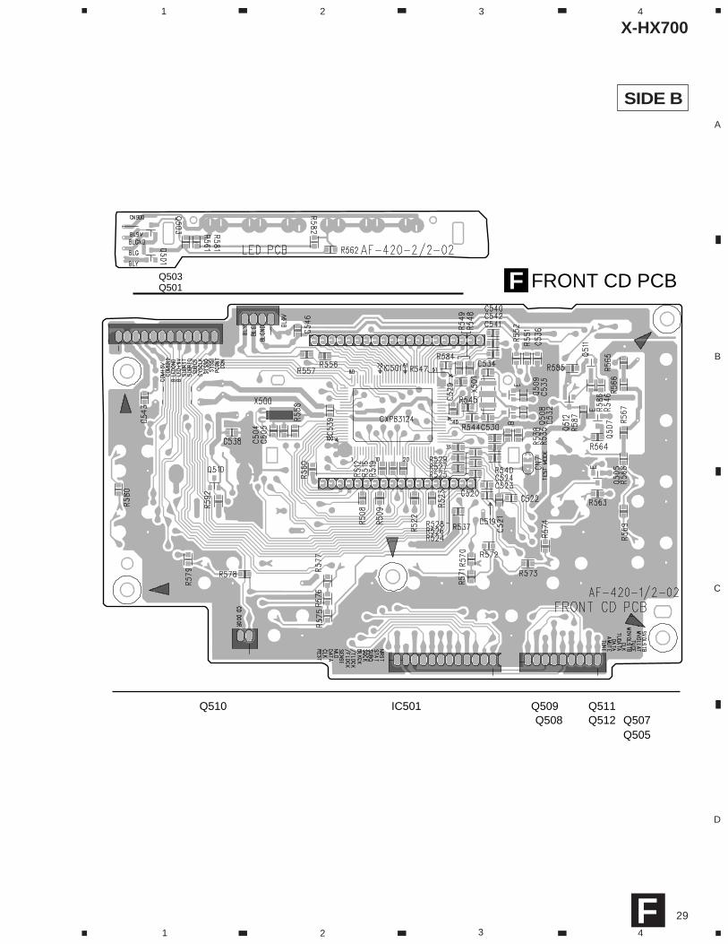
X-HX700
29
A
B
C
D
1 2 3 4
1 2 3 4
SIDE B
F
Q501Q503
Q510 IC501Q507Q505
Q511Q509Q512Q508
FRONT CD PCBF

X-HX700
30
NSP CD RECEIVER TUNER PCB 66675 CD PCB 66786 AMP COMBI PCB 66789
NSP POWER PCB • • • • •NSP FUSE PCB • • • • •NSP HEADPHONE PCB • • • • •
FRONT CD PCB 66788 CD MECHANISM ASSY 61417
TUNER PCB ASSYSEMICONDUCTORS
IC101, IC103 (TC9260P) 52189IC2 (BA1450S) 52190IC102 (BH3854AS) 52192IC3 (BU2614) 52193IC100 TC4052BP
Q4 2SA1037AKQ7 2SK118GRQ10, Q201 2SA933SQ101- Q104, Q200 2SC1740SQ1- Q2, Q5, Q6, Q9, Q202 2SC2412K
D6, D201- D207, D208 1SS133D2 (SVC384) 57713D1, D3 DA204KD7, D8– D10 (RB721Q) 51435U1 (FM Fronted) TFFJ2U581A
COILS AND FILTERSL1 AM ANT 839741L2 AM OSC 839739L7 FM DET 839737T1 AM IFT 839740L100-L104 AXIAL INDUCTOR LAU2R2J
C13 CHIP INDUCTOR LK2125R22K 52411
5. PCB PARTS LISTNOTES : ÷ Parts marked by “ NSP ” are generally unavailable because they are not in our Master Spare Parts List.
÷ The mark found on some component parts indicates the importance of the safety factor of the part.Therefore, when replacing, be sure to use parts of identical designation.
÷ When ordering resistors, first convert resistance values into code form as shown in the following examples.Ex. 1 When there are 2 effective digits (any digit apart from 0), such as 560 ohm and 47k ohm (tolerance is shown by
J = 5%, and K = 10%).560 Ω = 56 × 10 1 = 561 ...................................................RD1/4PU 5 6 1 J47k Ω = 47 × 10 3 = 473 ..................................................RD1/4PU 4 7 3 J0.5 Ω = R50 ......................................................................RN2H Â 5 0 K1 Ω = 1R0 .........................................................................RS1P 1 Â 0 K
Ex. 2 When there are 3 effective digits (such as in high precision metal film resistors).5.62k Ω = 562 × 10 1 = 5621...........................................RN1/4PC 5 6 2 1 F
LIST OF PCB ASSEMBLIES
Mark No. Description Parts No. Mark No. Description Parts No.
A
CAPACITORSC8, C12, C36, C209 (10µF/16V) 57213C4, C38, C75, C210, C212 (22µF/16V) 57216C50 CCPUSL180J50C43, C44 CCSQCH220J50C2 CCSQUJ220J50
C9, C15, C55 CCSQSL101J50C73, C74 CCSQSL151J50C23 CCSQYB102K50C7, C30, C201, C202, C208 CEAT101M10C213, C215, C205 CEAT101M10
C6, C11, C31 CEAT1R0M50C107, C108 CEAT2R2M50C34 CEAT3R3M50C203, C206 CEAT470M10C101- C106, C109- C112, C121 CEAT4R7M50
C122, C127, C128, C214, C221 CEAT4R7M50C33, C211 CEATR22M50C223- C225 CKPUYB101K50C51, C220, C222 CKPUYB102K50C53, C204, C226 CKPUYF104Z50
C20, C32, C207 CKPUYY473Z50C49, C52, C200 CKPUYK103K50C1 CKSQYB104K50C5, C25- C28, C35- C39, C41, C42 CKSQYB103K50C115, C116, C123, C124 CKSQYB152K50
C71, C72 CKSQYB153K50C45 CKSQYB331K50C10 CKSQYB682K50C54, C117, C118, C125, C126 CKSQYF104Z50C14, C24, C29 CKSQYF223Z50
C133,C134 CQMBA103J50C216 CQMBA223J50C129- C132 CQMBA683J50 TC1 TRIMMER CAPACITOR (10pF) 58003
RESISTORSR220, R221 RD1/4PU102JR107 RD1/4PU153JL8 RD1/8PU101JR108 RD1/8PU153JR8, R201, R211, R223, R224 RD1/8PU102J
X-HX700
31
R45 RD1/8PU222JR101– R104 RD1/8PU273JR200, R119, R120 RD1/8PU104JR121, R122 RD1/8PU152JR213,R105, R106, R222 RD1/8PU472J
R205– R207 RD1/8PU471JR42, R43, R202, R111– R118 RD1/8PU473JR210 RD1/8PU680JR123, R124, R129, R130 RD1/8PU682JR212 RD1/8PU272J
Other Resistors RS1/10S J
OTHERSCERAMIC FILTER SFE10 50508ACERAMIC FILTER SFU45 50518CN102 CONNECTOR (53254-0910) 51037CN101 CONNECTOR (5268-10A) 51038CN103 CONNECTOR (53253-1010) 51039
4P CABLE HOLDER 51048-0400PIN JACK YKC21-3035 52526CN5 PUSH TERMINAL YKD21 60243X1 CRYSTAL AT-38 (75kHz) 602444P CONNECTOR ASSY 66769
CD PCB ASSYSEMICONDUCTORS
IC400 (AN8806SB) 52103IC401 (BA6299FP) 52118IC402 (MN662741RHM) 52187Q400 2SA1037KQ402,Q403 2SC2412K
Q401 (2SB1561) 54651D401,D402 DAN202K
CAPACITORSC421 (0.1µF/25V) 56517C436 (0.33µF/25V) 56549C453- C455 (10µF/16V) 57212C414 (22µF/16V) 57112C439 CCSQCH100J50
C438 CCSQCH120J50C450 CCSQSL221J50C423, C457, C458 CCSQSL101J50C410 CCSQSL331J50C403, C404 CCSQSL471J50
C419 CCSQSL5R0D50C407 CEAT101M10C433 CEAT102M25C422 CEAT1R0M50C418, C430, C441, C442, C447 CEAT221M10
C408 CEAT2R2M50C448 CEATR47M50C400, C401, C434 CKSQYB102K50C415, C416, C449 CKSQYB103K50C409 CKSQYB122K50
C435 CKSQYB123K50
Mark No. Description Parts No. Mark No. Description Parts No.
C417, C425, C426, C428 CKSQYB222K50C412, C427, C429 CKSQYB223K50C413, C424, C451, C452 CKSQYB273K50C402, C440 CKSQYF104Z50C405, C412, C420, C427, C431 CKSQYF223Z50
C432, C437, C443, C445, C446, C429 CKSQYF223Z50
RESISTORSOther Resistors RS1/10S J
OTHERSX400 RESONATOR CSA16.93MX 60266424 CD PCB 66786CN400 CONNECTOR 52043-1810 51014CN406 CONNECTOR 53254-1210 51032CN401-CN403 51033
CONNECTOR S2B-PH-K-SCN407 CONNECTOR 53254-0310 51034CN404 CONNECTOR 53254-0410 51035CN405 CONNECTOR 53254-0610 51036
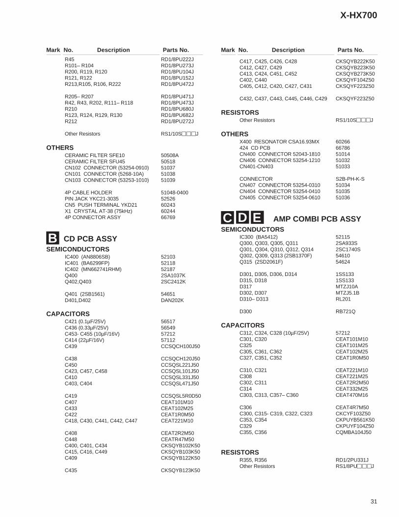
AMP COMBI PCB ASSYSEMICONDUCTORS
IC300 (BA5412) 52115Q300, Q303, Q305, Q311 2SA933SQ301, Q304, Q310, Q312, Q314 2SC1740SQ302, Q309, Q313 (2SB1370F) 54610Q315 (2SD2061F) 54624
D301, D305, D306, D314 1SS133D315, D318 1SS133D317 MTZJ10AD302, D307 MTZJ5.1BD310– D313 RL201
D300 RB721Q
CAPACITORSC312, C324, C328 (10µF/25V) 57212C301, C320 CEAT101M10C325 CEAT101M25C305, C361, C362 CEAT102M25C327, C351, C352 CEAT1R0M50
C310, C321 CEAT221M10C308 CEAT221M25C302, C311 CEAT2R2M50C314 CEAT332M25C303, C313, C357– C360 CEAT470M16
C306 CEAT4R7M50C300, C315- C319, C322, C323 CKCYF103Z50C353, C354 CKPUYB561K50C329 CKPUYF104Z50C355, C356 CQMBA104J50
RESISTORSR355, R356 RD1/2PU331JOther Resistors RS1/8PU J
B
C D E

X-HX700
32
OTHERSFUSE HOLDER FH-V-03078 51606
J302 HEADPHONE JACK 52513J303 1P PIN JACK YKB11-0940 52527J301 PUSH TERMINAL 4P 60246
AC TERMINAL 66745
AMP COMBI PCB 66789AMP PCB 66789AFUSE PCB 66789BH/P PCB 66789C
CN303 CONNECTOR 53254-1210 51032
CN301 CONNECTOR 5268-12A 51040CN305 CONNECTOR 5129-5A 51041CN302 6P CONNECTOR ASSY 66768CN306 3P CONNECTOR ASSY 66771CN300 10P CONNECTOR ASSY 66777
5P CONNECTOR 66767CABLE HOLDER (5P) 51052-0500GND PLATE 66676
FRONT CD PCB ASSYSEMICONDUCTORS
IC501 (CXP83232A) 52209Q508, Q509, Q511, Q512 2SC2412KQ507, Q510 (DTA114YKAT146) 54653Q501, Q503, Q505 DTC114YKD500- D505 (SLA380MT3F) 52907
D511 (SLR342MCTE7) 52908D510 (SLR342DCTE7) 52909D512 (SLR342VCTE7) 52910
SWITCHESSW500- SW518 (SOA-111H) 53426
COILSL501, L502 AXIAL INDUCTOR (10µH) LAU100J
CAPACITORSC504, C505 (30pF/50V) 56560C527 (10µF/50V) 57212C500- C526 CCSQSL101J50C530, C534 CCSQSL560J50C537 CEAT101M10
C528 CEAT471M10C529, C532, C535, C536, C539, C543 CKSQYB102K50C538, C540- C542, C546 CKSQYB103K50
RESISTORSOther Resistors RS1/10S J
Mark No. Description Parts No.
F
Mark No. Description Parts No.
OTHERSX501 RESONATOR CSTCC 50524 (4.19MHz)LCD500 LCD KSG4149(FTN) 52716IC500 REMOTE CONTROL RECEIVER 60124X500 CRYSTAL QRT-26 60245 (32.76kHz)
LCD HOLDER 66727 LCD SHEET 66756 FRONT CD COMBI PCB 66788 FRONT CD PCB 66788A LED PCB 66788B
CN504 CONNECTOR 53253-0410 51029CN500 CONNECTOR 53254-0210 51032CN503 CONNECTOR ASSY (12P) 66764CN501 CONNECTOR ASSY (12P) 66765CN502 CONNECTOR ASSY (9P) 66766
CN505 4P CONNECTOR 66770CN506 2P CONNECTOR 66772

X-HX700
33
6. ADJUSTMENT6.1 CD SECTION
Note : There is no information to be shown in this CD adjustment.
• Set the mode selector to FM BAND.• Connect the wiring as shown in Fig. 1, 2.
6.2 TUNER SECTION6.2.1 FM Tuner Section
• Set the mode selector to AM BAND.• Connect the wiring as shown in Fig. 1, 2.
6.2.2 AM Tuner Section
StepNo.
AdjustmentTitle
FM SG (1kHz, ± 75kHz dev.) Reception Frequency
Display
Adjustment Location SpecificationsFrequency
(MHz)Level
(dBmV)
1DET. waveformCoil Adjustment
98 60 98MHz L7
• Adjust L7 so that the voltaghe between TP8 (+)and TP9 (−) becomes 0V ± 50mV.
• Check the waveform with the oscilloscope, andconfirm so that the output level is about −11 ±2dBV and THD is about 0.5 ± 0.1%.Confirm that the "TUNE" indicator in the LCD isturned on.
StepNo.
AdjustmentTitle
AM SG (400Hz, 30% Mod.) Reception Frequency
Display
Adjustment Location SpecificationsFrequency
(kHz)Level
(dBmV/m)
1Vt(Tuning Voltage Adjustment)
531
1602
−
−
531kHz
1602kHz
L2
−
• Adjust L2 so that the voltage between TP6 (+) and TP7(−) becomes 1.0V.
• Set the reception frequency to 1602 kHz and confirmthat the voltage is about 6.1V.
2 IFT Adjustment 999 S/N about 10dB 999kHz T1
1. Connect an electrolytic capacitor of about 10µF to TP9 (TP9 side is +), and terminate with TP10 by a resistorof about 47kΩ. Connect the sweep input to the bothends of terminated resistor.
2. Adjust T1 so that the marker of 450kHz ± 3kHzbecomes the same level (single-peak characteristic ofIF becomes symmetrical).
3. Input 74dBµV from the SSG, confirm the waveform ofoutput signal so that the output level is −27 ± 2dBVand THD is about 1 ± 0.5%. And confirm that the"TUNE" indicator in the LCD is turned on.
3Tracking Adjustment
6031404
50(S/N about 10dB)
603kHz1404kHz
L1TC1
Connect an oscilloscope to TP3 (L) and TP4 (R), and adjust L1 (603kHz) and TC1 (1404kHz) repeatedly so that the output level becomes maximum.

X-HX700
34
AM SG
MPX SG FM SG PRODUCT DCVoltmeter
Oscilloscope
AM IF Sweep
FM75Ω antenna terminal
AM antenna terminal
60cm
Center Center
Loop antenna
Fig. 1 AM and FM Adjustment Wiring Diagram
Fig. 2 Adjustment Point
Point (TP) SIDE B show .
AM Loop antenna
TC1
TP3
TP5TP4
TP6 TP7
TP8
TP10
TP9TC2
L1
L2
L4
L5
L7T2
T1
TUNER PCBA SIDE A
FM antenna
7 Check and Adjustment

X-HX700
35
7. GENERAL INFORMATION7.1 DIAGNOSIS
CN407
CN202
CN404
CD RearCase
CN405
Leaf SW(Door)
TUNER PCB
Removethe Hook
Cut the Binder
CN406
POWER PCB
POWER PCB
TUNER PCBCD REAR CASE
× 51
× 21
× 42
× 21
× 24
× 33
× 51
1
2
2
5
3
4
7
6
3

X-HX700
36
CD PCB
CD Rear Case
Servo Mecha Assy
Holder Plate
CD MECHANISM ASSY
×41
× 32
4
3

X-HX700
37
7.2 PARTS7.2.1 IC
7 52193 (BU2614) (TUNER PCB ASSY : IC3)7 PLL IC
¶ Pin Arrangement ¶ Block Diagram
¶ The information shown in the list is basic information and may notcorrespond exactly to that shown in the schematic diagrams.
XOUT 1
XIN 2
CE 3
CK 4
DA 5
CD 6
P0 7
P1 8
16 VSS
15 PD1
14 VDD1
13 VDD2
12 FMIN
11 AMIN
10 P2
9 IF IN
• List of IC 52193 (BU2614), 52192 (BH3854AS), 52103 (AN8806SB), 52118 (BA6299FP), 52187 (MN662741RHM), 52206 (CXP83232A), 52186 (AK4518-VF-E2)

X-HX700
38
¶ Pin Function
No. Pin Name Function No. Pin Name Function
1 A_GND Analog ground 17 VREF 3.8V reference voltage output pin
2 IN1 1 ch volume input pin 18 LATCH Latch data reception pin
3 NF1 Gain adjustment pin of input stage amp. 19 DATA Data reception pin
4 BVN1
Pins for 1 ch low-pass filter connection
20 CK Clock reception pin
5 BIN1 21 BCTime constant install pins for change shock protection
6 BVO1 22 TC
7 TIN1Pins for 1 ch high-pass filter connection
23 VC
8 TVO1 24 OUT2 2 ch volume output pin
9 OUT1 1 ch volume output pin 25 TVO22 ch high-pass filter connection pins
10 Vcc Power supply pin 26 TIN2
11 SC Time constant install pin for change shock 27 BVO2
2 ch low-pass filter connection pins12 PORT1
Port output pins
28 BIN2
13 PORT2 29 BVN2
14 PORT3 30 NF2 Gain adjustment pin of input stage amp.
15 PORT4 31 IN2 2 ch volume input pin
16 D_GND Digital ground 32 FILTER Filter pin
(BASS) (TREBLE)
TONE
2kΩ 10kΩ
20kΩ
20kΩ
20kΩ
2kΩ200kΩ
20kΩ
47kΩ
47kΩ
10kΩ 10kΩ
CONTROL
RE
F. P
OW
ER
SU
PP
LY
MA
TR
IX •
SU
RR
OU
ND
VOLU
ME
VO
LUM
EV
OLU
ME
VOLU
ME
(BASS) (TREBLE)
TONE
52192 (BH3854AS) (TUNER PCB : IC102) • Main Control and TONE Control IC
• Block Diagram

X-HX700
39
52103 (AN8806SB) (CD PCB : IC400) • Digital Servo Head Amplifier IC
• Block Diagram
• Pin Function
No. Pin Name Function No. Pin Name Function
1 PD APC Amp input 19 ENV 3TENV output
2 LD APC Amp output 20 VREF VREF output
3 LD ON/OFF APC ON/OFF control 21 LD OFF APC OFF control
4 LDP APC reference voltage setting 22 VDET VDET output
5 Vcc Power supply pin 23 TEBPF VDET input
6 RF- RF Amp inverting input 24 CROSS CROSS output
7 RFOUT RF Amp output 25 TEOUT TE. Amp output
8 RFIN AGC input 26 TE- TE. Amp inverting input
9 CAGC AGC loop filter connection pin 27 FEOUT FE. Amp output
10 ARF AGC output 28 FE- FE. Amp inverting input
11 CENV Capacitor connection pin for RF detection 29 FBAL F. BAL control
12 CEA Capacitor connection pin for HPF-Amp 30 TBAL T. BAL control
13 CSBDO Capacitor connection pin for RF dark side envelope 31 PDFRI-V Amp conversion resistor adjustment
14 BDO BDO output 32 PDER
15 CSHRT Capacitor connection pin for RF light side envelope 33 E
I-V Amp input16 OFTR OFTR output 34 F
17 RFDET RFDET output 35 B+D
18 GND Ground 36 A+C
6 7 29 27 28 8 9 10 17 11 12 19
13
14
15
16
5
18
20
21
2
341222326252430
33
32
34
31
35
36
EQ AGCRFDETEC-TION
ENVDETECTION
BDO
OFTR
RF- RFOUT FBAL FEOUT FE- RFIN CAGC ARF RFDET CENV CEA ENV
CSBDO
BDO
CSHRT
OFTR
Vcc
GND
VREF
LD OFF
LD
LD ON/OFFLDPPDVDETTEBPFTE-TEOUTCROSSTBAL
E
PDER
F
PDFR
B+D
A+C
SUBTRACTION
FEOUT by IA+CFEOUT by IB+DFEOUT by FBAL
TEOUT by IFTEOUT by IEFEOUT by TBAL

X-HX700
40
28 27 26 25 24 23 22 21 20 19 18 17 16 15
1 2 3 4 5 6 7 8 9 10 11 12 13 14
THERMALSHUTDOWN
GN
D
VC
C
GN
D
OP-AMP. VC
C
DR
IVE
RM
UT
E
DR
IVE
RC
H3
DR
IVE
RC
H4
DR
IVE
RC
H1
DR
IVE
RC
H2
No. Pin Name Function No. Pin Name Function1 VIN1 CH1 input 15 VO4 + CH4 positive output
2 VIN1' CH1 gain change 16 VO4 - CH4 negative output
3 VIN2 CH2 input 17 VO3 + CH3 positive output
4 VIN2' CH2 gain change 18 VO3 - CH3 negative output
5 OPOUT OP Amp output 19 MUTE Mute control
6 OPIN - OP Amp negative input 20 VCC VCC
7 OPIN + OP Amp positive input 21 GND Sub-straight GND
8 GND Sub-straight GND 22 RGND GND (regulator GND)
9 VCC VCC 23 REGB External TR base connection pin
10 BIAS Bias input 24 REGOUT 5V output (connect a external PNP Tr collector)
11 VO2 - CH2 negative output 25 VIN3' CH3 gain change
12 VO2 + CH2 positive output 26 VIN3 CH3 input
13 VO1 - CH1 negative output 27 VIN4' CH4 gain change
14 VO1 + CH1 positive output 28 VIN4 CH4 input
52118 (BA6299FP) (CD PCB : IC401) • CD Driver IC
• Block Diagram
• Pin Function

X-HX700
41
79LRCKIN (MSEL)
80BCLKIN (SSEL)
78SRDATAIN (PSEL)
70IOSEL
66CLVS
67CRC
13BLKCK
62/CLDCK
56SBCK
55SUBC
68DEMPH
69RESY
...FLAG6 (RESY)
80SSEL
14SQCK
46DRF
44ARF
76RSEL
78PSEL
9MLD
15SUBQ
53PCK
52EFM
48PLLF
47DSLF
45IREF
52CK384 (EFM)
49VCOF
61BYTCK
19SMCK
63FCLK
20PMCK
77CSEL
79MSEL
59X2
17STAT
58X1
60V
DD
57V
SS
4D
VD
D1
5D
VS
S1
18/R
ST
71/T
ES
T
32F
E
33T
E
34R
FE
NV
37T
RC
RS
35V
DE
T
39B
DO
38/R
FD
ET
36O
FT
51AVSS2
50AVDD2
75 OUTR
73 OUTL
72 AVDD1
74 AVSS1
DIG
ITA
L D
EE
MP
HA
SIS
SU
BC
OD
EB
UF
FE
R
CIR
C E
RR
OR
CO
RR
EC
TIO
ND
EIN
TE
RLE
VE
16k
SR
AM
DIG
ITA
LA
UD
IOIN
TE
RF
AC
E
CLV
SE
RV
O
INT
ER
PO
LAT
ION
SO
FT
MU
TIN
GD
IGIT
AL
AT
TE
NU
AT
ION
PE
AK
DE
TE
CT
AU
TO
CU
E
DS
L •
PLL
VC
OV
CO
MIC
RO
CO
MP
UT
ER
INT
ER
FA
CE
SE
RV
O C
PU D
/AC
ON
VE
RT
ER
OU
TP
UT
PO
RT
TIM
ING
GE
NE
RA
TO
RP
ITC
H C
ON
TR
OL
EF
M D
EM
OD
ULA
TIO
N
SY
NC
INT
ER
PO
LAT
ION
SU
BC
OD
E D
EM
OD
ULA
TIO
N
1 bi
t DA
CLO
GIC
S
PW
M(R
)P
WM
(L)
8TIM
ES
OV
ER
SA
MP
LIN
GD
IGIT
AL
FIL
TE
R
65 FLAG64 IPFLAP
6 TX
24 ECM
23 PC
2 LRCK
3 SRDATA
1 BCLK
21 TRV26 KICK29 VREF61 (BYTCK) TRVSTP25 ECS22 TVD27 TRD28 FOD31 TBAL30 FBAL54 TOFS41 TES12 /TLOCK11 /FLOCK42 PLAY40 LDON43 WVEL10 SENSE
16 DMUTE
7MCLK
8MDATA
A/D CONVERTER INPUT PORT SERVO TIMINGGENERATOR
52187 (MN662741RHM) (CD PCB : IC402) • DSP IC
• Block Diagram

X-HX700
42
No. Pin Name I/O Function No. Pin Name I/O Function
1 BCLK O Bit clock output for SRDATA 31 TBAL O Tracking balance adjustment output
2 LRCK OL, R discrimination signal outputH: Lch audio data , L: Rch audio data
32 FE I Focus error signal input (analog input)
3 SRDATA O Serial data output 33 TE I Tracking error signal input (analog input)
4 DVDD1 I Power supply for digital circuit 34 RFENV I RF envelope signal input (analog input)
5 DVSS1 I Ground for digital circuit 35 VDET I Vibration detection signal input (H: detection)
6 TX O Digital audio interface output signal 36 OFT I Off track signal input (H: Off track)
7 MCLK IMicrocomputer command clock signal input(Data latches at rising edge.)
37 TRCRS I Track cross signal input
8 MDATA I Microcomputer command data input 38 /RFDET I RF detection signal input (L: detection)
9 MLD I Microcomputer command load signal input L: 39 BDO I Drop out signal input (H: drop out)
10 SENSE OSense signal output (OFT, FESL, NACEND, NAJEND, SFG, NWTEND)
40 LDON O Laser ON signal outputÅiH: ON)
11 /FLOCK O Focus servo incoming signal (L:incoming 41 TES O Tracking error shunt signal output (H: shunt)
12 /TLOCK O Tracking servo incoming signal (L:incoming 42 PLAY O Play signal output (H: PLAY)
13 BLKCK O Subcode block clock signal (fBLKCK=75Hz) 43 WVEL O Double speed status signal output
14 SQCK I External clock input for subcode Q register 44 ARF I RF signal input
15 SUBQ O Subcode Q data output 45 IREF I Reference current input
16 DMUTE I Muting output H:Mute 46 DRF I Bias pin for DSL
17 STAT OStatus signal (CRC, CUE, CLVS, TTSTOP, FCLV, SQOK, FLAG6, SENSE, /FLOCK, /TLOCK)
47 DSLF I/O Loop filter pin for DSL
18 /RST IReset input (Reset at IOSEL=L and more than472ns) L:Reset
48 PLLF I/O Loop filter pin for PLL
19 SMCK OWhen MSEL=H, 8.4672MHz clock signal output 49 VCOF I/O Loop filter pin for VCO
20 PMCK O 88.2kHz clock signal output 50 AVDD2 IPower supply for analog circuit(for DSL, PLL, AD input and DA output)
21 TRV O Traverse forced forward output 51 AVSS2 IGND for analog circuit(for DSL, PLL, AD input and DA output)
22 TVD O Traverse drive output 52 EFM OEFM signal output When IOSEL=H, EFM signal output. When IOSEL=L,
23 PC O Spindle motor ON signal L: ON 53 PCK O PLL extract clock output (fPCK=4.32MHz)
24 ECM OSpindle motor drive signal (forced mode output) 3-state
54 TOFS O Tracking offset adjustment output
25 ECS OSpindle motor drive signal (servo error signal output)
55 SUBC O Subcode serial output
26 KICK O Kick pulse output 3-state 56 SBCK IClock input for subcode serial output(with pull-up resistor)
27 TRD O Trscking drive output 57 VSS I GND for oscillation circuit
28 FOD O Focus drive output 58 X1 ICrystal oscillation circuit input(f=16.9344MHz, 33.8688MHz)
29 VREF IReference voltage for DA output section(TVD, ECS, TRD, FOD, FBAL, TBAL, TOFS)
59 X2 OCrystal oscillation circuit output(f=16.9344MHz, 33.8688MHz)
30 FBAL O Focus balance adjustment output 60 VDD I Power supply for oscillation circuit
• Pin Function

X-HX700
43
No. Pin Name I/O Function No. Pin Name I/O Function
61 BYTCK OWhen IOSEL=H, byte clock signal outputWhen IOSEL=L, Traverse STOP signal outputH: STOP mode
71 /TEST I Test pin (Normal: H)
62 /CLDCK OSubcode frame clock signal output(fCLDCK=7.35kHz)
72 AVDD1 IPower supply for analog circuit [for audio output (use both as L ch and R ch)]
63 FCLK OCrustal frame clock signal output(fFCLK=7.35kHz)
73 OUTL O L ch audio output
64 IPFLAG O Interpolate flag signal output H: Interpolate 74 AVSS1 IGround for analog circuit [for audio output (use both as L ch and R ch)]
65 FLAG O Flag signal output 75 OUTR O R ch audio output
66 CLVS OPhase sync. state signal output of spindle servo H: CLV , L: Rough servo
76 RSEL IRF signal polarity specify pin When light level is "H", RSEL=H When light level is "L", RSEL=L
67 CRC OSubcode CRC check result outputH: OK , L: NG
77 CSEL ICrystal oscillator frequency specify pinH : Oscillation frequency = 33.8688MHzL : Oscillation frequency = 16.9344MHz
68 DEMPH O Deemphasis detection signal output H: ON 78 PSEL IWhen IOSEL=H, test pin (normal: L)When IOSEL=L, SRDATA input
69 RESY O
When IOSEL=H, playback sync signal RESY output of frame sync. H: synchronize, L: not synchronizeWhen IOSEL=L, address reset signal FLAG6 output of RAM for deinterleave.L: generate address reset
79 MSEL I
When IOSEL=H, SMCK pin output frequency switch H : SMCK= 8.4672MHz
L : SMCK= 4.2336MHzWhen IOSEL=L, LRCK inputH: Lch data, L: Rch dataSMCK= 4.2336MHz fixed
70 IOSEL I Mode switch pin 80 SSEL I
When IOSEL=H, SUBQpin output mode switch H: Q code buffer use modeWhen IOSEL=L, BCLK inputQ code buffer mode fixed
• Pin Function

X-HX700
44
52206 (CXP83232A) (FRONT CD PCB : IC501) • System Microcomputer IC
• Pin Arrangement (Top view)

X-HX700
45
• Block Diagram

X-HX700
46
• Pin Function
FunctionNo. Pin Name I/O1 PE2/INT2 I Port (E) / External interrupt request input
2 PE3/INT3/NMI I Port (E) / External interrupt request input / Nonmaskable interrupt input
3 PE4/RMC I Port (E) / Remote control reception circuit input
4 PE5/PWM O Port (E) / 14 bit PWM output
5 PE6/TO/ADJ O Port (E) / 16 bit timer/Rectangle waveform output of counter (duty 50% output) /32 kHz oscillation frequency
6 PB0/CINT I/O 8 bit input/output port (port B) / 16 bit timer / External capture input of counter
7 PB1/CS0 I/O 8 bit input/output port (port B) / Chip select input of serial interface (CH0)
8 PB2/SCK0 I/O 8 bit input/output port (port B) / serial interface (CH0) input/output
9 PB3/SI0 I/O 8 bit input/output port (port B) / serial data (CH0) input
10 PB4/SO0 I/O 8 bit input/output port (port B) / serial data (CH0) output
11 PB5/SCK1 I/O 8 bit input/output port (port B) / serial clock (CH1) input/output
12 PB6/SI1 I/O 8 bit input/output port (port B) / serial data (CH1) input
13 PB7/SO1 I/O 8 bit input/output port (port B) / serial data (CH1) output
14 PC0
I/O 8 bit input/output port (port C)
15 PC1
16 PC2
17 PC3
18 PC4
19 PC5
20 PC6
21 PC7
22 PH0
I/O 8 bit input/output port (port H)
23 PH1
24 PH2
25 PH3
26 PH4
27 PH5
28 PH6
29 PH7
30 PA0/AN0
I/O 8 bit input/output port (port A) / Analog input to A/D converter
31 PA1/AN1
32 PA2/AN2
33 PA3/AN3
34 PA4/AN4
35 PA5/AN5
36 PA6/AN6
37 PA7/AN7
38 RST I System reset of "L" level active
39 EXTAL1 I Crystal connection pin for system clock oscillation When apply a clock from the external, input to EXTAL1 pin and input the reverse clock to XTAL1 pin.System clock oscillation use for normal operation mode (Max. 10MHz).40 XTAL1 −
41 VSS − GND pin
42 XTAL2 − Crystal connection pin for system clock oscillation When apply a clock from the external, input to EXTAL2 pin and input the reverse clock to XTAL2 pin.System clock oscillation use for sub-clock mode (Typ. 500kHz).43 EXTAL2 I
44 AVREF − Reference voltage input of A/D converter
45 AVSS − GND pin of A/D converter
46 VL O Control pin for cutoff the current which flows to the bias resistor for external LCD at standby.
47 VLC3 −Bias power supply pin for LCD48 VLC2 −
49 VLC1 −50 COM0 O Common signal output pin for LCD

X-HX700
47
• Pin Function
No. Pin Name I/O Function51 COM1
O Common signal output for LCD52 COM2
53 COM3
54 SEG0
O Segment signal output for LCD
55 SEG1
56 SEG2
57 SEG3
58 SEG4
59 SEG5
60 SEG6
61 SEG7
62 SEG8
63 SEG9
64 SEG10
65 SEG11
66 SEG12
67 SEG13
68 SEG14
69 SEG15
70 SEG16/PD0
O 8 bit output port (port D) / Segment signal output for LCD
71 SEG17/PD1
72 SEG18/PD2
73 SEG19/PD3
74 SEG20/PD4
75 SEG21/PD5
76 SEG22/PD6
77 DEG23/PD7
78 SEG24/PF0
O 8 bit output port (port F) / Segment signal output for LCD
79 SEG25/PF1
80 SEG26/PF2
81 SEG27/PF3
82 SEG28/PF4
83 SEG29/PF5
84 SEG30/PF6
85 SEG31/PF7
86 SEG32/PG0
O 8 bit output port (port G) / Segment signal output for LCD87 SEG33/PG1
88 SEG34/PG2
89 VDD − Positive power supply pin
90 NC − NC pin Connect to VDD at normal operation.
91 VSS − GND pin
92 TX O Crystal connection pin of the clock generating circuit for 32kHz timer counter Connect a 32.768kHz crystal between TEX and TX. When using for event input, connect the source of clock generation to TEX and TX pin set to open.93 TEX I
94 SEG35/PG3
O 8 bit output port (port G) / Segment signal output for LCD
95 SEG36/PG4
96 SEG37/PG5
97 SEG38/PG6
98 SEG39/PG7
99 PE0/INT0/EC0I (Port E) / External interrupt request input / Timer / External event input of the timer
100 PE1/INT1/EC1
X-HX700
48
38 19
181
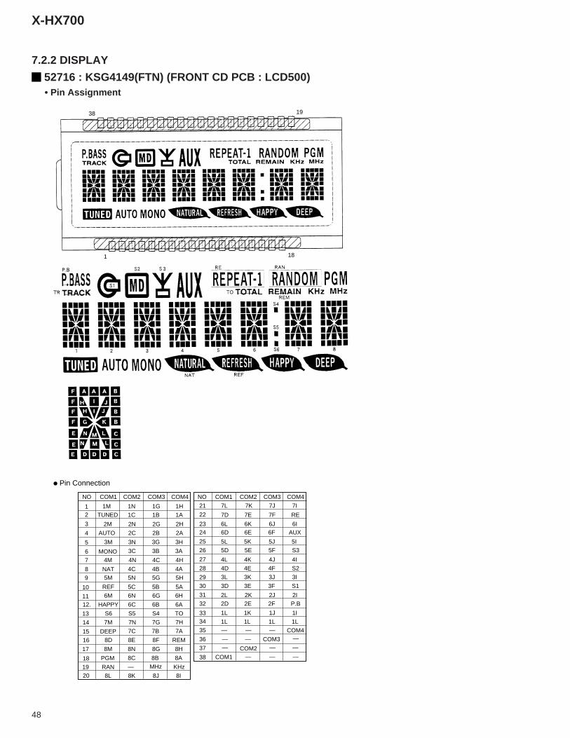
NO
12
3
4
5
6
7
8
9
10
21 7L
7D
6L6D
5L
5D
4L
4D
3L
3D
2L2D
1L
1L 1L 1L 1L— — —
———— — —
— — —
COM4
COM3
COM2COM1
1K 1J 1I
2E 2F P.B2K 2J 2I
3E 3F S1
3K 3J 3I
4E 4F S2
4K 4J 4I
5E 5F S3
5K 5J 5I
6E 6F AUX6K 6J 6I
7E 7F RE
7K 7J 7I
22
2324
25
26
27
28
29
30
31
32
3334
35
36
37
38
1112.
13
14
15
16
17
181920
COM1
TUNED
AUTO
MONO
1M 1N 1G 1H1A1B1C
2M 2N
2C
3M 3N
3C
4M
NAT
REF
REM
PGMMHz KHzRAN
HAPPY
DEEP
4N
4C
5M
6M 6N
7M
7C
8D
8M 8N
8C
8L 8K 8J 8I
—
8B 8A
8G 8H
8E 8F
7B 7A
7N 7G 7H
6C
S6 S5 S4 TO
6B 6A
6G 6H
5N
5C 5B 5A
5G 5H
4B 4A
4C 4H
3B 3A
3G 3H
2B 2A
2G 2H
COM2 COM3 COM4 COM1 COM2 COM3 COM4NO
÷ Pin Connection
52716 : KSG4149(FTN) (FRONT CD PCB : LCD500) • Pin Assignment
7.2.2 DISPLAY
X-HX700
49
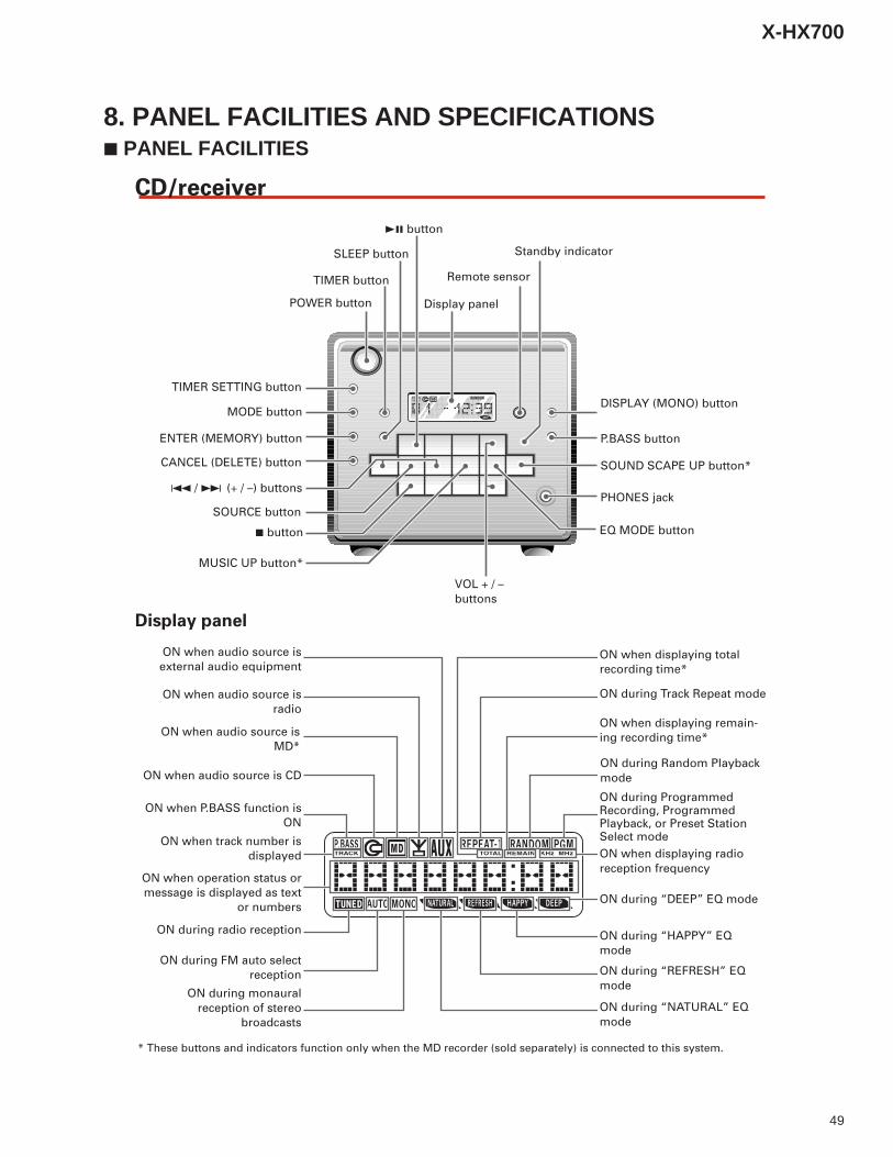
8. PANEL FACILITIES AND SPECIFICATIONS7 PANEL FACILITIES
CD/receiver
Display panel
Remote sensor
Standby indicator
38 button
SLEEP button
TIMER button
POWER button
TIMER SETTING button
MODE button
ENTER (MEMORY) button
CANCEL (DELETE) button
4 / ¢ (+ / –) buttons
SOURCE button
7 button
MUSIC UP button*
DISPLAY (MONO) button
P.BASS button
SOUND SCAPE UP button*
PHONES jack
EQ MODE button
VOL + / –buttons
Display panel
* These buttons and indicators function only when the MD recorder (sold separately) is connected to this system.
ON when audio source isexternal audio equipment
ON when audio source isradio
ON when audio source isMD*
ON when audio source is CD
ON when P.BASS function isON
ON when track number isdisplayed
ON when operation status ormessage is displayed as text
or numbers
ON during radio reception
ON during FM auto selectreception
ON during monauralreception of stereo
broadcasts
ON when displaying totalrecording time*
ON during Track Repeat mode
ON when displaying remain-ing recording time*
ON during Random Playbackmode
ON during ProgrammedRecording, ProgrammedPlayback, or Preset StationSelect modeON when displaying radioreception frequency
ON during “DEEP” EQ mode
ON during “HAPPY” EQmode
ON during “REFRESH” EQmode
ON during “NATURAL” EQmode

X-HX700
50
Remote Control
* All buttons of the MD section, the SOUND SCAPE UP button and the MUSIC UP button function only when the MDrecorder (sold separately) is connected to this system. See the Operating Instructions of the MD recorder for thedetailed operation of these buttons.
SLEEP button
TIMER button
CD section
38 button
4 / ¢ buttons
ENTER button
MODE button7 button
MD section*
38 button
4 / ¢ buttons
SOUNDSCAPE button
MODE button
7 button
VOL + / – buttons
SOUND SCAPE UP button*
MUSIC UP button*
EQ MODE button
+ / – buttons
FM/AM button
Radio section
STANDBY/ONbutton

X-HX700
51
• Specifications and design subject to possiblemodification without notice, due toimprovements.
CD/receiver
CD player unit
Type ......................... Compact disc audio system
Medium................................... Compact disc (CD)
No. of channels ................................ Two (stereo)
Program steps ................................................... 32
Amplifier unit
Maximum practical output (RMS)
.................. 5 W + 5 W (1 kHz, T.H.D. 10 %, 4 Ω)
FM (UKW)/AM (MW/LW) tuner
section
Reception frequency
FM ....... 87.50 to 108.00 MHz in 50-kHz steps
FMW ...... 88.0 to 108.0 MHz in 100-kHz steps
AM ................ 531 to 1,602 kHz in 9-kHz steps
AMW .......... 530 to 1,600 kHz in 10-kHz steps
Antenna
AM ............................. Loop antenna (supplied)
FM .................................. 75 Ω unbalanced type(extends from rear of set)
Specifications
Power supply, etc.
Power supply voltage
............................................. AC 230 V, 50/60 Hz
Power consumption (based on electricalproduct regulations) ..................................... 30 W
Power consumption in standby mode
...................................................... less than 3 W
External dimensions
........................ 145 (W) × 137 (H) × 250 (D) mm
(5 3/4 (W) × 5 1/2 (H) × 9 7/8 (D) inches)
Weight ................................... 2.6 kg (5 lb 11.7 oz)
Speaker system
Type ........................ Book-shelf style, bass reflextype magnetically shielded
Speakers ................... 10-cm full range cone type
Nominal impedance ........................................ 4 Ω
Playback frequency range ......... 50 Hz to 20 kHz
Maximum input ............................................ 25 W
External dimensions
........................ 145 (W) × 137 (H) × 200 (D) mm
(5 3/4 (W) × 5 1/2 (H) × 7 7/8 (D) inches)
Weight ......................... 1.3 kg (2 lb 13.8 oz) each
* Measured pursuant to the Federal TradeCommissions’s Trade Regulation rule on PowerOutput Claims for Amplifier.
** Measured by Audio Spectrum Analyzer.
Accessories
Dry cell batteries(AA/R6P)
Remote control unit(60231A)
AM LoopAntenna(60232)
• Operating instructions
Related Documents