CCS Technology Synopsys Interoperability Forum November 9, 2005 Bill Mullen Vice President of Engineering Synopsys, Inc.

CCS Technical
Oct 26, 2014
Welcome message from author
This document is posted to help you gain knowledge. Please leave a comment to let me know what you think about it! Share it to your friends and learn new things together.
Transcript
CCS Technology
Synopsys Interoperability ForumNovember 9, 2005
Bill MullenVice President of EngineeringSynopsys, Inc.
© 2005 Synopsys, Inc. (2)
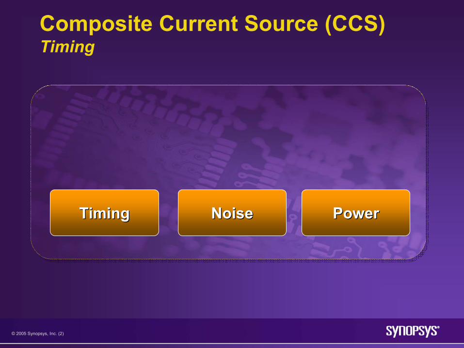
Composite Current Source (CCS)Timing
NoiseNoise PowerPowerTimingTiming
© 2005 Synopsys, Inc. (3)
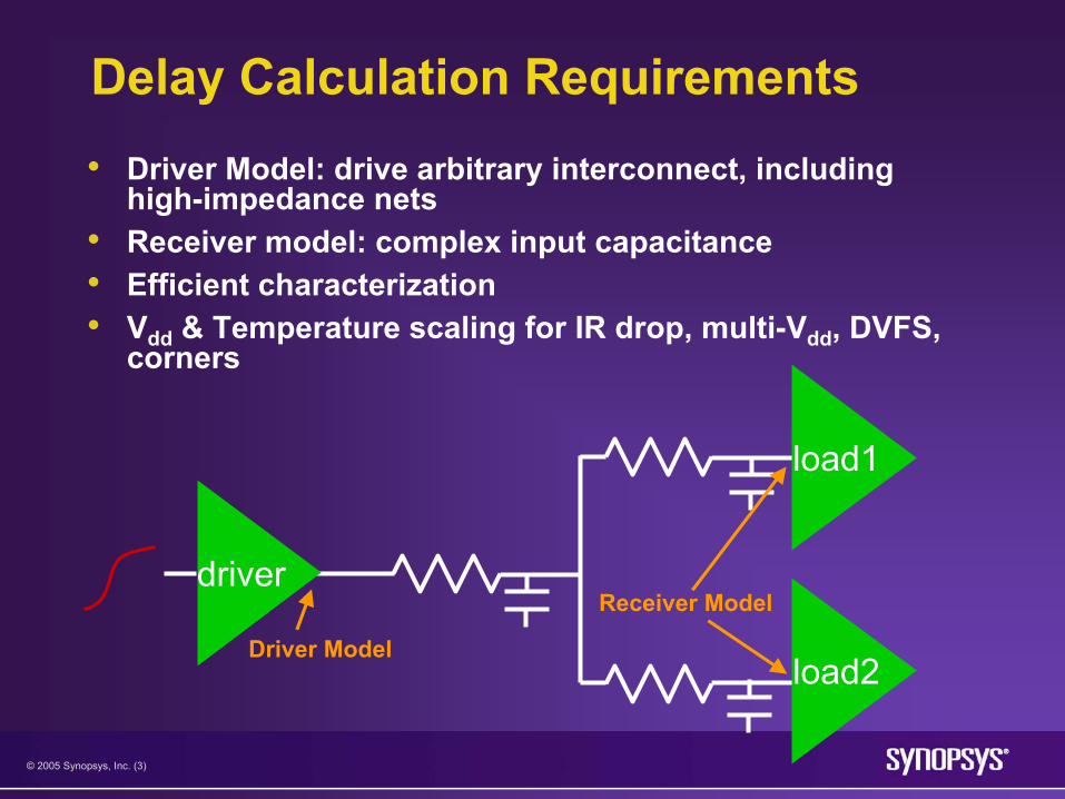
Delay Calculation Requirements• Driver Model: drive arbitrary interconnect, including
high-impedance nets• Receiver model: complex input capacitance• Efficient characterization• Vdd & Temperature scaling for IR drop, multi-Vdd, DVFS,
corners
driver
load1
load2Driver Model
Receiver Model
© 2005 Synopsys, Inc. (4)
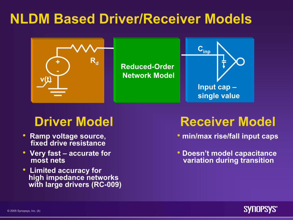
NLDM Based Driver/Receiver Models
Driver Model• Ramp voltage source,
fixed drive resistance• Very fast – accurate for
most nets• Limited accuracy for
high impedance networks with large drivers (RC-009)
Receiver Model• min/max rise/fall input caps
• Doesn’t model capacitance variation during transition
Reduced-OrderNetwork Modelv(t)
+-
Rd
Input cap –single value
Cinp
© 2005 Synopsys, Inc. (5)
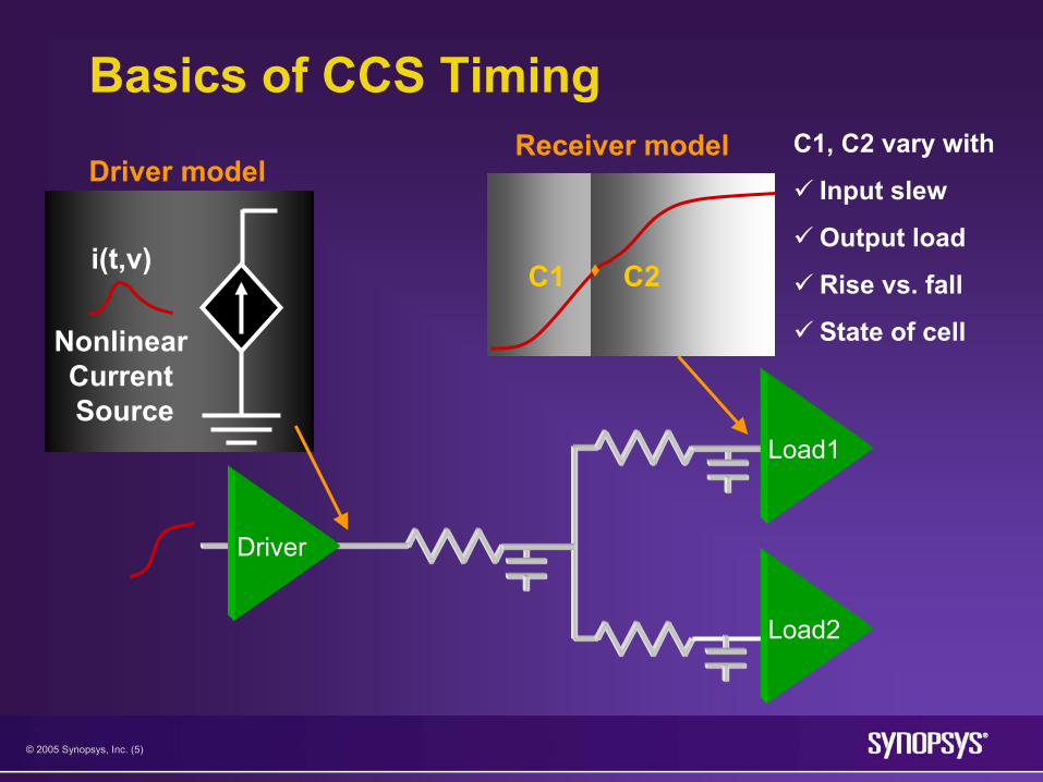
Basics of CCS Timing
C1 C2
Receiver model
i(t,v)
Nonlinear Current Source
Driver model
Load1
Load2
Driver
C1, C2 vary with
Input slew
Output load
Rise vs. fall
State of cell
© 2005 Synopsys, Inc. (6)
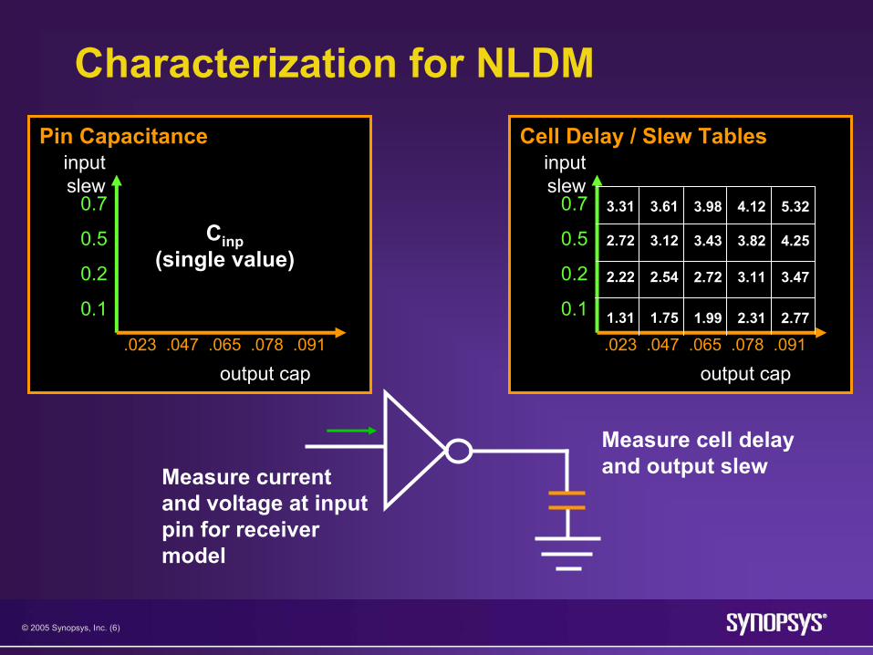
Cell Delay / Slew Tables
Characterization for NLDM
output cap
inputslew
0.7
0.5
0.2
0.1
.023 .047 .065 .078 .091
Measure cell delay and output slew Measure current
and voltage at input pin for receiver model
Pin Capacitance
output cap
inputslew
0.7
0.5
0.2
0.1
.023 .047 .065 .078 .091
Cinp(single value)
3.313.31 3.613.61 3.983.98 4.124.12 5.325.32
2.722.72 3.123.12 3.433.43 3.823.82 4.254.25
2.222.22 2.542.54 2.722.72 3.113.11 3.473.47
1.311.31 1.751.75 1.991.99 2.312.31 2.772.77
© 2005 Synopsys, Inc. (7)
Driver Model
Characterization for CCS Timing
output cap
inputslew
0.7
0.5
0.2
0.1
.023 .047 .065 .078 .091
Measure current through load cap for driver modelMeasure current
and voltage at input pin for receiver model
Receiver Model
output cap
inputslew
0.7
0.5
0.2
0.1
.023 .047 .065 .078 .091
C1,C2
C1,C2
C1,C2
C1,C2
C1,C2
C1,C2
C1,C2
C1,C2
C1,C2
C1,C2
C1,C2
C1,C2
C1,C2
C1,C2
C1,C2
C1,C2
C1,C2
C1,C2
C1,C2
C1,C2
© 2005 Synopsys, Inc. (8)
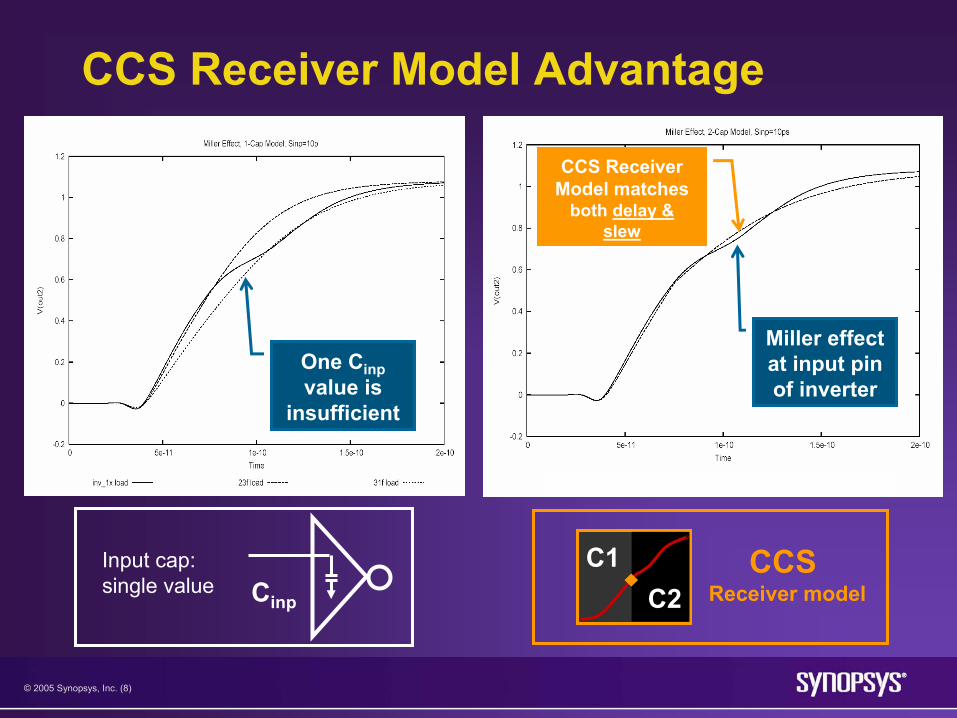
CCS Receiver Model Advantage
Miller effect at input pin of inverter
CCS Receiver Model matches
both delay & slew
C1C2
CCS Receiver model
One Cinpvalue is
insufficient
Input cap:single value Cinp
© 2005 Synopsys, Inc. (9)
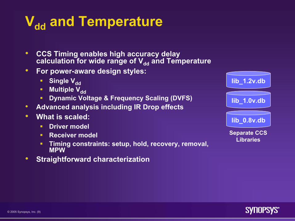
Vdd and Temperature
• CCS Timing enables high accuracy delay calculation for wide range of Vdd and Temperature
• For power-aware design styles:Single VddMultiple VddDynamic Voltage & Frequency Scaling (DVFS)
• Advanced analysis including IR Drop effects• What is scaled:
Driver modelReceiver modelTiming constraints: setup, hold, recovery, removal, MPW
• Straightforward characterization
lib_0.8v.db
lib_1.0v.db
lib_1.2v.db
Separate CCSLibraries
© 2005 Synopsys, Inc. (10)
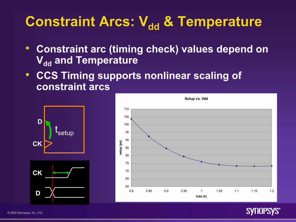
Constraint Arcs: Vdd & Temperature
• Constraint arc (timing check) values depend on Vdd and Temperature
• CCS Timing supports nonlinear scaling of constraint arcs
tsetup
Setup vs. Vdd
60
65
70
75
80
85
90
95
100
105
110
0.8 0.85 0.9 0.95 1 1.05 1.1 1.15 1.2
Vdd (V)
setu
p (p
s)CK
D
CK
D
CCS Timing Results
© 2005 Synopsys, Inc. (12)
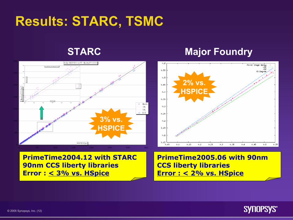
Results: STARC, TSMC
Delay (HSPICE vs PT-liberty,PT-CCS)
0
500
1000
1500
2000
2500
3000
3500
0 500 1000 1500 2000 2500 3000 3500
HSPICE[ps]
liberty,CCS[ps]
liberty
-3%
+3%
CCS
Delay (HSPICE vs PT-liberty,PT-CCS)
600
650
700
750
800
850
900
600 650 700 750 800 850 900
HSPICE[ps]
liberty,CCS[ps]
liberty
-3%
+3%
CCS
PrimeTime2004.12 with STARC 90nm CCS liberty librariesError : < 3% vs. HSpice
STARC Major Foundry
3% vs.HSPICE
2% vs.HSPICE
PrimeTime2005.06 with 90nm CCS liberty librariesError : < 2% vs. HSpice
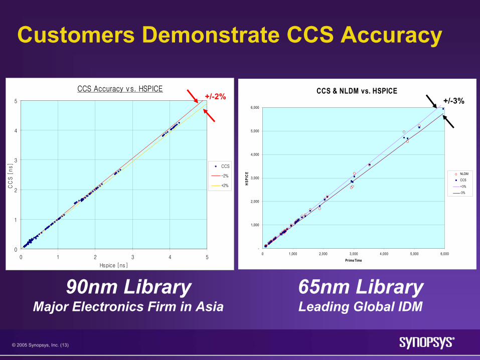
© 2005 Synopsys, Inc. (13)
90nm LibraryMajor Electronics Firm in Asia
CCS Accuracy v s. HSPICE
0
1
2
3
4
5
0 1 2 3 4 5
Hspice [ns]
CC
S [
ns] CCS
-2%
+2%
+/-2%
Customers Demonstrate CCS Accuracy
65nm LibraryLeading Global IDM
CCS & NLDM vs. HSPICE
-
1,000
2,000
3,000
4,000
5,000
6,000
0 1,000 2,000 3,000 4,000 5,000 6,000
PrimeTime
HSP
ICE NLDM
CCS
+3%
-3%
+/-3%
© 2005 Synopsys, Inc. (14)
CCS Timing Summary
• High accuracy delay and slew calculationAdvanced driver and receiver modelingResults within 2% of SPICEPowerful scaling for Vdd and Temperature
• No impact on analysis runtime• Easy and efficient characterization• Industry Support
ARM, TSMC, Virage Logic, STARC, Library Technologies, Synopsys NanoChar

© 2005 Synopsys, Inc. (15)
Composite Current Source (CCS)Noise
NoiseNoise PowerPowerTimingTiming
© 2005 Synopsys, Inc. (16)
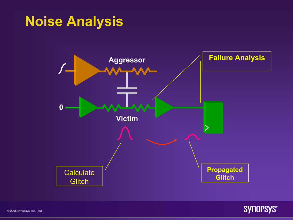
Noise Analysis
Aggressor
0Victim
Calculate Glitch
Propagated Glitch
Failure Analysis
© 2005 Synopsys, Inc. (17)
Noise Modeling Requirements
• Accurate model to support:Noise bump calculationNoise propagationDriver weakening (combination of propagated and injected bumps)Vdd and Temperature scaling
• Characterization should be fast and cover a broad set of cell types
• Model must enable efficient calculation in analysis and implementation tools
© 2005 Synopsys, Inc. (18)
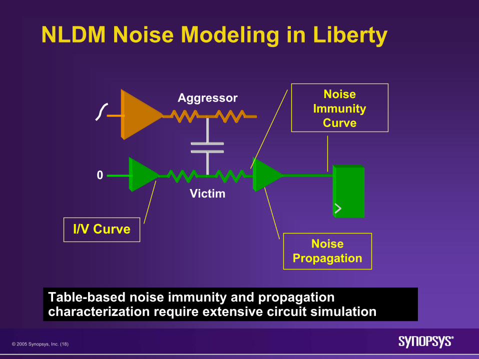
NLDM Noise Modeling in Liberty
Aggressor
0Victim
I/V CurveNoise
Propagation
Noise Immunity
Curve
Table-based noise immunity and propagation characterization require extensive circuit simulation
© 2005 Synopsys, Inc. (19)
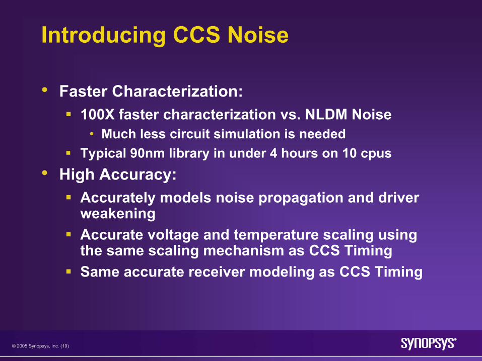
Introducing CCS Noise
• Faster Characterization:100X faster characterization vs. NLDM Noise
• Much less circuit simulation is neededTypical 90nm library in under 4 hours on 10 cpus
• High Accuracy:Accurately models noise propagation and driver weakeningAccurate voltage and temperature scaling using the same scaling mechanism as CCS TimingSame accurate receiver modeling as CCS Timing
© 2005 Synopsys, Inc. (20)
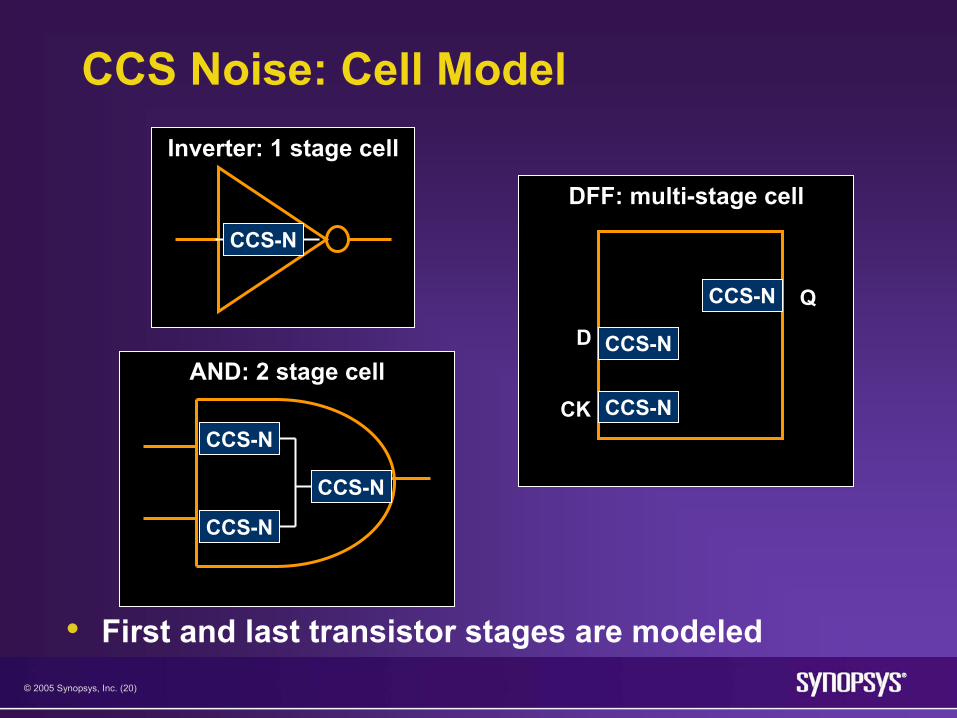
DFF: multi-stage cell
CK
D
Q
CCS Noise: Cell Model
• First and last transistor stages are modeled
Inverter: 1 stage cell
AND: 2 stage cell
CCS-N
CCS-N
CCS-N
CCS-N
CCS-N
CCS-N
CCS-N
© 2005 Synopsys, Inc. (21)
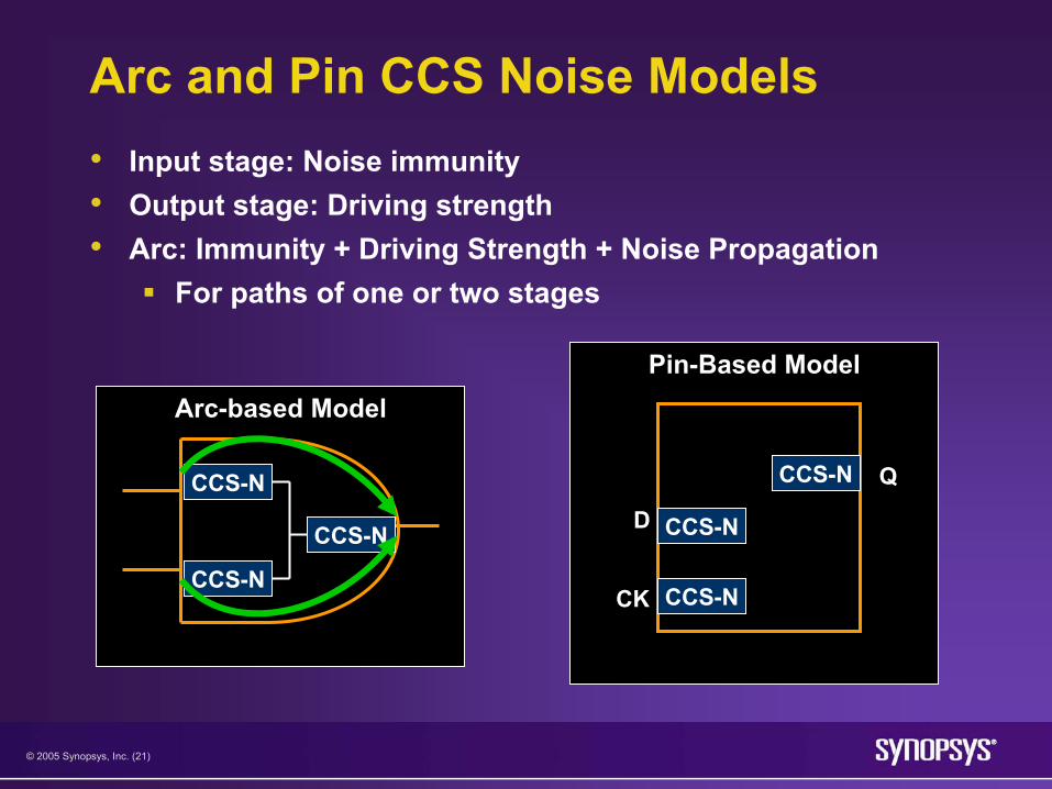
Pin-Based Model
CK
D
Q
Arc and Pin CCS Noise Models• Input stage: Noise immunity• Output stage: Driving strength• Arc: Immunity + Driving Strength + Noise Propagation
For paths of one or two stages
Arc-based Model
CCS-N
CCS-N
CCS-N
CCS-N
CCS-N
CCS-N

© 2005 Synopsys, Inc. (22)
Arc-Based Example: AND2
A2
A1
CCS-N
CCS-N
CCS-NA1
A2
ZZN_7
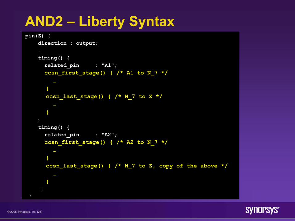
© 2005 Synopsys, Inc. (23)
AND2 – Liberty Syntaxpin(Z) {
direction : output;…timing() {related_pin : "A1";ccsn_first_stage() { /* A1 to N_7 */
…}ccsn_last_stage() { /* N_7 to Z */…
}}timing() {related_pin : "A2";ccsn_first_stage() { /* A2 to N_7 */
…}ccsn_last_stage() { /* N_7 to Z, copy of the above */…
}}
}
© 2005 Synopsys, Inc. (24)
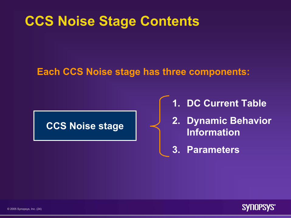
CCS Noise Stage Contents
CCS Noise stage
Each CCS Noise stage has three components:
1. DC Current Table
2. Dynamic Behavior Information
3. Parameters
© 2005 Synopsys, Inc. (25)
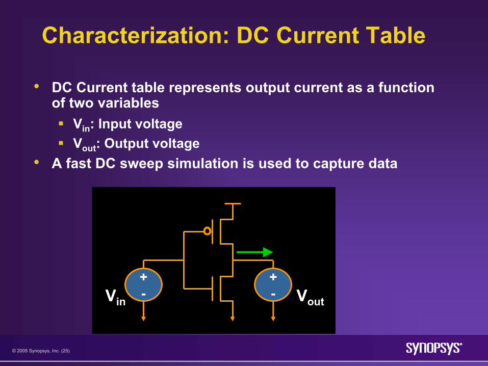
Characterization: DC Current Table
• DC Current table represents output current as a function of two variables
Vin: Input voltageVout: Output voltage
• A fast DC sweep simulation is used to capture data
Vin Vout
+-
+-
© 2005 Synopsys, Inc. (26)
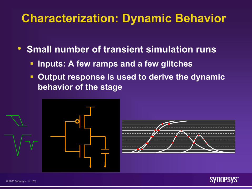
Characterization: Dynamic Behavior
• Small number of transient simulation runsInputs: A few ramps and a few glitchesOutput response is used to derive the dynamic behavior of the stage
© 2005 Synopsys, Inc. (27)
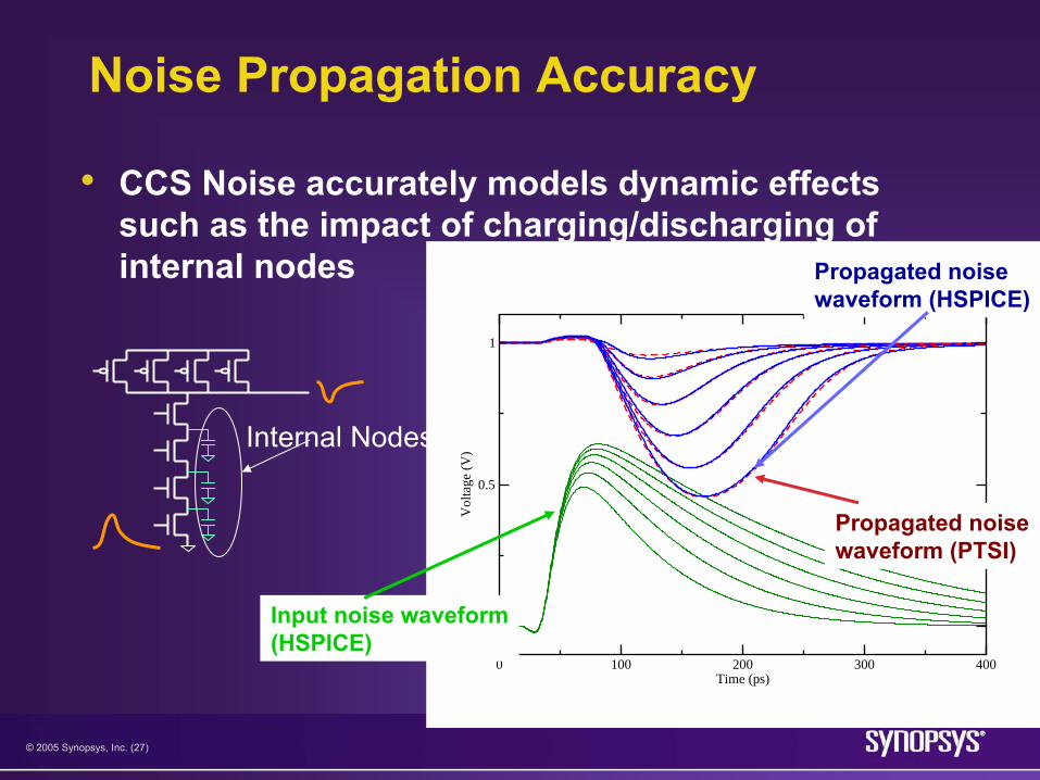
Noise Propagation Accuracy
• CCS Noise accurately models dynamic effects such as the impact of charging/discharging of internal nodes
0 100 200 300 400Time (ps)
0
0.5
1
Vol
tage
(V
)
Input noise waveform(HSPICE)
Propagated noisewaveform (HSPICE)
Propagated noisewaveform (PTSI)
Internal Nodes
© 2005 Synopsys, Inc. (28)
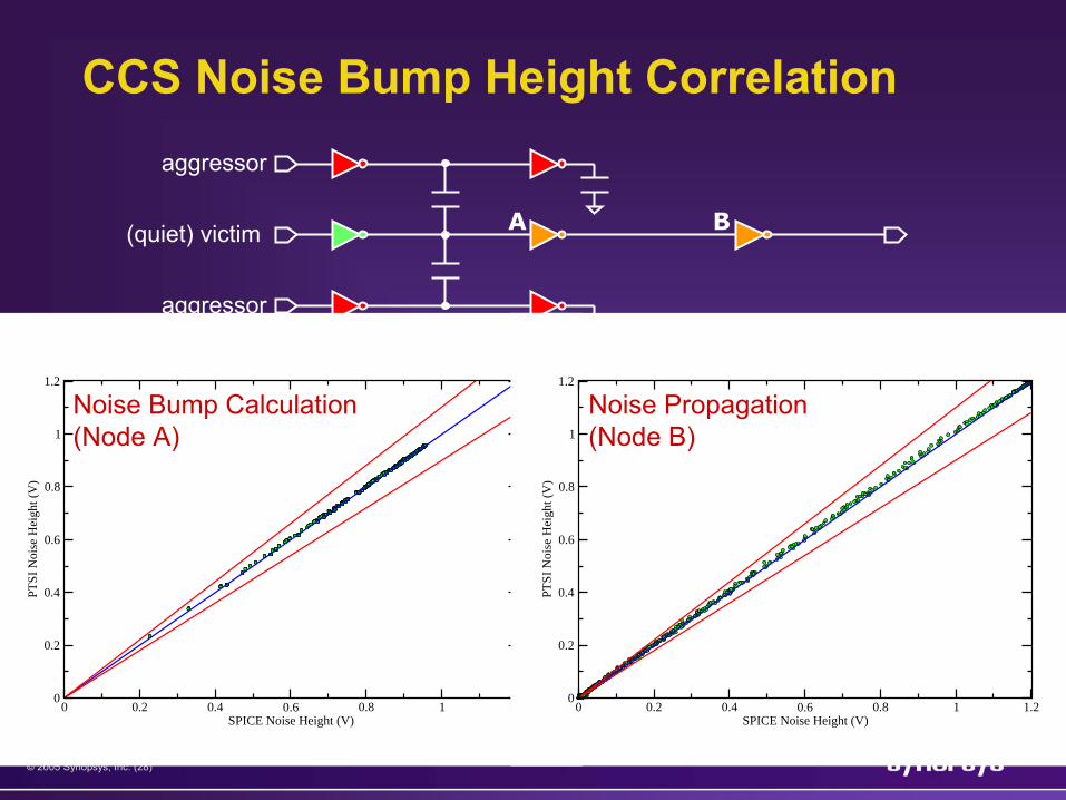
CCS Noise Bump Height Correlation
A B
0 0.2 0.4 0.6 0.8 1 1.2SPICE Noise Height (V)
0
0.2
0.4
0.6
0.8
1
1.2
PTSI
Noi
se H
eigh
t (V
)
0 0.2 0.4 0.6 0.8 1 1.2SPICE Noise Height (V)
0
0.2
0.4
0.6
0.8
1
1.2
PTSI
Noi
se H
eigh
t (V
)
Noise Bump Calculation(Node A)
Noise Propagation(Node B)
aggressor
(quiet) victim
aggressor
© 2005 Synopsys, Inc. (29)
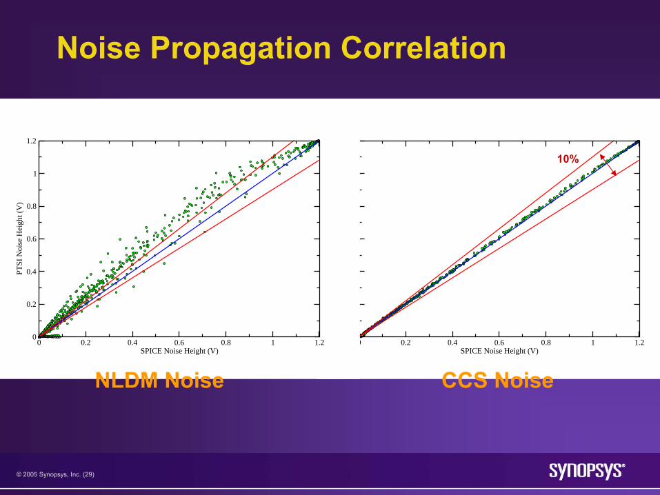
Noise Propagation Correlation
0 0.2 0.4 0.6 0.8 1 1.2SPICE Noise Height (V)
0
0.2
0.4
0.6
0.8
1
1.2
PTSI
Noi
se H
eigh
t (V
)0 0.2 0.4 0.6 0.8 1 1.2
SPICE Noise Height (V)
0
0.2
0.4
0.6
0.8
1
1.2
PTSI
Noi
se H
eigh
t (V
)
CCS NoiseNLDM Noise
10%
© 2005 Synopsys, Inc. (30)
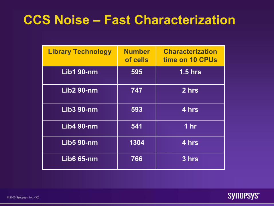
CCS Noise – Fast Characterization
3 hrs
4 hrs
1 hr
4 hrs
2 hrs
1.5 hrs
Characterization time on 10 CPUs
1304Lib5 90-nm
541Lib4 90-nm
593Lib3 90-nm
766Lib6 65-nm
Number of cells
Library Technology
747Lib2 90-nm
595Lib1 90-nm
© 2005 Synopsys, Inc. (31)
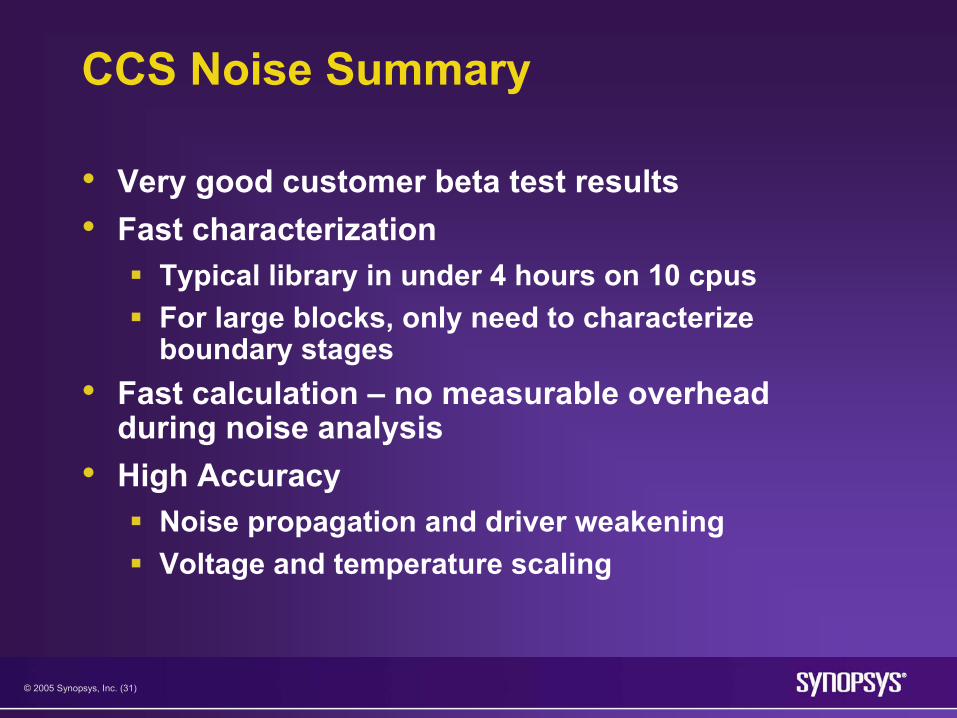
CCS Noise Summary
• Very good customer beta test results• Fast characterization
Typical library in under 4 hours on 10 cpusFor large blocks, only need to characterize boundary stages
• Fast calculation – no measurable overhead during noise analysis
• High AccuracyNoise propagation and driver weakeningVoltage and temperature scaling

© 2005 Synopsys, Inc. (32)
Composite Current Source (CCS)Power
NoiseNoise PowerPowerTimingTiming

© 2005 Synopsys, Inc. (33)
Power Library Requirements
• Address needs of Multi-Voltage designsMulti-Rail cells (Vdd, Vss)Non-zero ground railMTCMOS (power gating)
• Static and dynamic rail analysisSupport accurate voltage (IR) drop calculation
• Single library / model for all power related applications
• Fast and easy library characterization

© 2005 Synopsys, Inc. (34)
Power Gating (MTCMOS)Reduce Leakage by turning block off
Block ABlock A
Block CBlock C
Block BBlock B
Power switch controlPower switch control
MTCMOSMTCMOS
VirtualVdd
Sleep-mode
VsleepVVdddd
LVtIN OUT
Sleep
Fine Grain:Fine Grain:Sleep transistor within each cellSleep transistor within each cell
VD
DV
SS
VDD
INTERNAL VSS INTERNAL VSS
Coarse Grain:Coarse Grain:Sleep transistor for entire blockSleep transistor for entire block
Challenge: Analyze “in-rush current” when block turns on

© 2005 Synopsys, Inc. (35)
Introducing CCS Power
• Switching current waveform for each power or ground pinFiner time resolutionFull Multi-Voltage support
• Equivalent parasitics as seen from the power networkAllows fast yet accurate rail analysis
• Support for macro power modeling for memory and IP• Unified library model for power optimization, power
analysis, rail analysisFast and easy to characterize

© 2005 Synopsys, Inc. (36)
Characterization for NLPMLiberty Non-Linear Power Model
inputslew
0.7
0.5
0.2
0.1
.023 .047 .065 .078 .091
3.613.61 3.983.98 4.124.12 5.325.32
2.722.72 3.123.12 3.433.43 3.823.82 4.254.25
2.222.22 2.542.54 2.722.72 3.113.11 3.473.47
1.311.31 1.751.75 1.991.99 2.312.31 2.772.77
output cap
3.313.31
Leakage power per state
Internal Energy per transition

© 2005 Synopsys, Inc. (37)
Characterization for CCS Power
i(t)
Dynamic Current Dynamic Current Waveform per Waveform per
transition per Railtransition per Rail
output cap
inputslew
0.7
0.5
0.2
0.1
.023 .047 .065 .078 .091Leakage current per state per rail
Can characterize CCS Power switching information concurrently with CCS Timing

© 2005 Synopsys, Inc. (38)
CCS Power Characterization• HSPICE Simulation: AND gate with rising input
Power pin (Vdd) currentPower pin (Vdd) currentGround pin (Vss) currentGround pin (Vss) current

© 2005 Synopsys, Inc. (39)
Advantages: Time Resolution
• Captures complete power and ground pin current waveforms
Charge/energy can be calculated by integrating current
( ) ( )( )∑∫
= −
−−
−+∞ −
+−+
≈n
i nn
nnnii
ii
IIttIttIIIdt
1 1
11
1
0 ln2

© 2005 Synopsys, Inc. (40)
Dynamic Rail Analysis
• Compute instance-specific voltage drop at all power/ground pins
• Requires cell model for switching and non-switching cases
VDD1
GND
RparCpar

© 2005 Synopsys, Inc. (41)
Equivalent Parasitics for Non-Switching Case• Essential for accurate rail analysis – additional decoupling cap• Cpar per input state for each power or ground pin• Rpar per input state for each power or ground pin to each output
CintIN2
IN1
OUT
Rpar
Cpar CloadCload
Equivalent Parasitics

© 2005 Synopsys, Inc. (42)
CCS Power Summary
• Single Power Model For All Power Applications: Power Optimization, Dynamic Rail Analysis, Power Analysis
• Accurately Models:Transient current during switchingEquivalent parasitics for non-switching caseLeakage current Multi-Voltage designs
• Multi-rail cells• Non-zero ground rail
MTCMOS: fine-grain or coarse-grain• Characterized concurrently with CCS Timing

© 2005 Synopsys, Inc. (43)
CCS SummaryContinuing With A Tradition Of Innovation
NoiseNoise PowerPowerTimingTiming
• CCS - Next Generation Modeling TechnologyOpen SourceUnified Model For Timing, Noise and PowerHigher Accuracy as Needed By 90nm and Below
• Easy and Efficient Library Characterization• Complete Ecosystem: Models, Format, Characterization

© 2005 Synopsys, Inc. (44)
Technical Collateral Material
• Technical collateral material for CCS is available on:www.synopsys.com/products/solutions/galaxy/ccs/cc_source.html
• It includes:CCS BackgrounderWhite PapersFormat SpecificationFAQ
Related Documents