ECS Journal of Solid State Science and Technology, 3 (4) R53-R59 (2014) R53 2162-8769/2014/3(4)/R53/7/$31.00 © The Electrochemical Society Cathodoluminescence of Double Layers of Phosphor Particles Daniel den Engelsen, Paul Harris, Terry Ireland, z and Jack Silver z Centre for Phosphor and Display Materials, Wolfson Centre for Materials Processing, Brunel University, Uxbridge, Middlesex UB8 3PH, United Kingdom We present radiance measurements of particle layers of ZnO:Zn, Y 2 O 3 :Eu and Y 2 O 2 S:Eu bombarded with electrons at anode voltages between 1 and 15 kV. The layers described in this work refer to single component layers, double layers and two component mixtures. The phosphor layers are deposited on ITO-coated glass slides by settling; the efficiency of the cathodoluminescence is determined by summing the radiances and luminances in the reflected and transmitted modes respectively. The efficiency of a double layer of Y 2 O 3 :Eu on top of ZnO:Zn at high electron energy is significantly larger than the efficiency of a corresponding layer in which the two components are mixed. This result is interpreted in terms of the penetration-model, which predicts a larger efficiency for a high-voltage phosphor on top of a low-voltage phosphor. When a layer of the low-voltage phosphor ZnO:Zn is on top of the high-voltage phosphor Y 2 O 3 :Eu, we also observe a higher efficiency than that of the corresponding layer with both components mixed. In this case the efficiency increases due to suppression of charging in the Y 2 O 3 :Eu layer. Double layers of ZnO:Zn and Y 2 O 2 S:Eu did not show enhanced efficiency, because the size of the Y 2 O 2 S:Eu particles was too large to evoke the penetration effect. © 2014 The Electrochemical Society. [DOI: 10.1149/2.021404jss] All rights reserved. Manuscript submitted January 20, 2014; revised manuscript received February 12, 2014. Published February 22, 2014. Recently we have described an idea to enhance the efficiency of cathodoluminescence (CL) of phosphor particle layers by depositing one layer on top of another. 1 Such an enhancement is to be expected when a high-voltage phosphor is deposited on top of a low-voltage phosphor. The difference between a high- and low-voltage phosphor is the light output at low electron beam energies: a low-voltage phosphor has a high luminance yield, whilst the luminance of a high-voltage phosphor is low. At higher voltages, however, the high-voltage phos- phor has the greatest output. As primary electrons penetrate the phos- phor they progressively lose energy until they can no longer excite the phosphor. When the top, high-voltage, layer is thin enough to allow electrons of sufficient energy (but not enough to excite the high energy one) to penetrate into the low-voltage phosphor layer enhancement of the luminance may be expected. We shall refer to this theory as the “penetration model”. An application of electron penetration in double and multi lay- ers of phosphors were so-called “penetrons”: Penetration CRTs, in which the color of the cathodoluminescence could be tuned by changing the energy of the electron beam. 2–4 The objective of the scientists who developed penetrons was to maximize the color gamut of the tubes; no attention was paid to enhancing the lumen output. If the energy of the electron beam is not high enough, the electrons do not pass through the top layer and there will be no enhancement of the luminance. This was the main reason that there was no observable increase of the lumen efficacy of a thin layer of nano-sized Y 2 O 3 :Eu particles on top of a ZnO: Zn layer using electron beam energies up to 5 Kv. 1 Another reason was the charging of non-conducting Y 2 O 3 :Eu layers upon electron bombardment. In order to cope with the charging of phosphor layers the measuring method was modified. Recently we published a new measuring method (the “comparison method”) to determine the CL of an insulating phosphor layer. 5 The objective of the work described here, was to investigate the effect of double layers of phosphor particles on the lumen and energy efficiency by using electron beam energies up to 15 kV and applying the comparison measuring method. The underlying motive to study the effect of double and multi layers of phosphor particles is to enhance the luminous efficiency. Besides the penetration model mentioned above, there are two other ways to enhance the light output of phosphor layers by CL. The first way is well described in the literature and is based on increasing the conductivity of phosphor layers. The charging of insulating phosphor layers is thought to be detrimental for a number of reasons. In most circumstances it is likely to charge negatively and this will result z E-mail: [email protected]; [email protected] in the deceleration of the beam before it strikes the phosphor. The field may also cause beam deflection, and may alter the transport of electrons within the phosphor layer. It may also establish fields inside the phosphor grains that impede the recombination of electrons and holes, resulting in a higher proportion of the energy being lost via non-radiative de-excitation routes. At anode voltages > 7 kV the application of aluminum (Al) back- ing layers is beneficial: preventing charging of the phosphor layer and enhancing the light output of the screen by reflection of the excited light directed to the vacuum side of the screen. At low anode voltages, however, an Al backing layer cannot be used, because too much of the electron beam is dissipated inside the metallic layer. In this case an alternative method of minimizing charging must be used and one approach is the mixing of the luminescent powder with In 2 O 3 powder, which is sufficiently conductive and does not absorb light at wave- lengths > 430 nm. 6–9 At first sight it might reasonably be expected that diluting the phosphor layer with non-luminescent material would reduce the efficiency of the layer. It appears, however, that the effects of charging are very strong and, for example, Yang and Yokoyama 7 found that the CL of ZnGa 2 O 4 powder could be enhanced by a factor of 4.2 by mixing with 12% In 2 O 3 powder. Xu et al. 8 found that the CL intensity of Lu 3 Ga 5 O 12 :Tb increased by almost a factor of 2 by mixing the luminescent powder with 5% In 2 O 3 nanoparticles. Hu et al. 9 coated Y 2 O 3 :Eu particles with In 2 O 3 and measured an increase of the light output by a factor of 1.5. One way of avoiding the losses caused by dilution is to use a conductive component that itself contributes to the luminescence (i.e. a conductive phosphor). In making double layers of (slightly) con- ductive ZnO:Zn and non-conductive Y 2 O 3 :Eu, the situation is more complicated, since both the penetration and the conductivity mod- els for the enhancement of the light output have to be taken into account. This complication is an important issue and will be con- sidered in discussing our measurement results. Since the Y 2 O 3 :Eu material used in this work consisted of nanosized powders, the de- position of powder layers by settling takes a long time and fabri- cating mixed layers is impossible due to segregation of ZnO:Zn and Y 2 O 3 :Eu. Therefore micrometer sized Y 2 O 2 S:Eu was included in this study. The second alternative to enhance the light output is making mixed layers of a CL and photoluminescent (PL) phosphor, in which the near UV or deep blue light of the CL component is used to excite the PL phosphor. This principle was demonstrated by Jung and Han 10 for Y 2 SiO 5 :Ce, a CL phosphor that emits in the near UV/deep blue region, and BaMgAl 10 O 17 :Eu, being a well-known blue emitting PL phosphor. Results and a discussion thereof are presented in the subsequent section. The final section contains the conclusions. ) unless CC License in place (see abstract). ecsdl.org/site/terms_use address. Redistribution subject to ECS terms of use (see 131.155.202.42 Downloaded on 2014-03-13 to IP

Welcome message from author
This document is posted to help you gain knowledge. Please leave a comment to let me know what you think about it! Share it to your friends and learn new things together.
Transcript

ECS Journal of Solid State Science and Technology, 3 (4) R53-R59 (2014) R532162-8769/2014/3(4)/R53/7/$31.00 © The Electrochemical Society
Cathodoluminescence of Double Layers of Phosphor ParticlesDaniel den Engelsen, Paul Harris, Terry Ireland,z and Jack Silverz
Centre for Phosphor and Display Materials, Wolfson Centre for Materials Processing, Brunel University, Uxbridge,Middlesex UB8 3PH, United Kingdom
We present radiance measurements of particle layers of ZnO:Zn, Y2O3:Eu and Y2O2S:Eu bombarded with electrons at anodevoltages between 1 and 15 kV. The layers described in this work refer to single component layers, double layers and two componentmixtures. The phosphor layers are deposited on ITO-coated glass slides by settling; the efficiency of the cathodoluminescence isdetermined by summing the radiances and luminances in the reflected and transmitted modes respectively. The efficiency of a doublelayer of Y2O3:Eu on top of ZnO:Zn at high electron energy is significantly larger than the efficiency of a corresponding layer inwhich the two components are mixed. This result is interpreted in terms of the penetration-model, which predicts a larger efficiencyfor a high-voltage phosphor on top of a low-voltage phosphor. When a layer of the low-voltage phosphor ZnO:Zn is on top of thehigh-voltage phosphor Y2O3:Eu, we also observe a higher efficiency than that of the corresponding layer with both componentsmixed. In this case the efficiency increases due to suppression of charging in the Y2O3:Eu layer. Double layers of ZnO:Zn andY2O2S:Eu did not show enhanced efficiency, because the size of the Y2O2S:Eu particles was too large to evoke the penetrationeffect.© 2014 The Electrochemical Society. [DOI: 10.1149/2.021404jss] All rights reserved.
Manuscript submitted January 20, 2014; revised manuscript received February 12, 2014. Published February 22, 2014.
Recently we have described an idea to enhance the efficiency ofcathodoluminescence (CL) of phosphor particle layers by depositingone layer on top of another.1 Such an enhancement is to be expectedwhen a high-voltage phosphor is deposited on top of a low-voltagephosphor. The difference between a high- and low-voltage phosphor isthe light output at low electron beam energies: a low-voltage phosphorhas a high luminance yield, whilst the luminance of a high-voltagephosphor is low. At higher voltages, however, the high-voltage phos-phor has the greatest output. As primary electrons penetrate the phos-phor they progressively lose energy until they can no longer excite thephosphor. When the top, high-voltage, layer is thin enough to allowelectrons of sufficient energy (but not enough to excite the high energyone) to penetrate into the low-voltage phosphor layer enhancement ofthe luminance may be expected. We shall refer to this theory as the“penetration model”.
An application of electron penetration in double and multi lay-ers of phosphors were so-called “penetrons”: Penetration CRTs,in which the color of the cathodoluminescence could be tunedby changing the energy of the electron beam.2–4 The objective ofthe scientists who developed penetrons was to maximize the colorgamut of the tubes; no attention was paid to enhancing the lumenoutput.
If the energy of the electron beam is not high enough, the electronsdo not pass through the top layer and there will be no enhancement ofthe luminance. This was the main reason that there was no observableincrease of the lumen efficacy of a thin layer of nano-sized Y2O3:Euparticles on top of a ZnO: Zn layer using electron beam energies up to5 Kv.1 Another reason was the charging of non-conducting Y2O3:Eulayers upon electron bombardment. In order to cope with the chargingof phosphor layers the measuring method was modified. Recently wepublished a new measuring method (the “comparison method”) todetermine the CL of an insulating phosphor layer.5 The objective ofthe work described here, was to investigate the effect of double layersof phosphor particles on the lumen and energy efficiency by usingelectron beam energies up to 15 kV and applying the comparisonmeasuring method.
The underlying motive to study the effect of double and multilayers of phosphor particles is to enhance the luminous efficiency.Besides the penetration model mentioned above, there are two otherways to enhance the light output of phosphor layers by CL. The firstway is well described in the literature and is based on increasing theconductivity of phosphor layers. The charging of insulating phosphorlayers is thought to be detrimental for a number of reasons. In mostcircumstances it is likely to charge negatively and this will result
zE-mail: [email protected]; [email protected]
in the deceleration of the beam before it strikes the phosphor. Thefield may also cause beam deflection, and may alter the transport ofelectrons within the phosphor layer. It may also establish fields insidethe phosphor grains that impede the recombination of electrons andholes, resulting in a higher proportion of the energy being lost vianon-radiative de-excitation routes.
At anode voltages > 7 kV the application of aluminum (Al) back-ing layers is beneficial: preventing charging of the phosphor layer andenhancing the light output of the screen by reflection of the excitedlight directed to the vacuum side of the screen. At low anode voltages,however, an Al backing layer cannot be used, because too much ofthe electron beam is dissipated inside the metallic layer. In this casean alternative method of minimizing charging must be used and oneapproach is the mixing of the luminescent powder with In2O3 powder,which is sufficiently conductive and does not absorb light at wave-lengths > 430 nm.6–9 At first sight it might reasonably be expectedthat diluting the phosphor layer with non-luminescent material wouldreduce the efficiency of the layer. It appears, however, that the effectsof charging are very strong and, for example, Yang and Yokoyama7
found that the CL of ZnGa2O4 powder could be enhanced by a factorof 4.2 by mixing with 12% In2O3 powder. Xu et al.8 found that theCL intensity of Lu3Ga5O12:Tb increased by almost a factor of 2 bymixing the luminescent powder with 5% In2O3 nanoparticles. Hu etal.9 coated Y2O3:Eu particles with In2O3 and measured an increase ofthe light output by a factor of 1.5.
One way of avoiding the losses caused by dilution is to use aconductive component that itself contributes to the luminescence (i.e.a conductive phosphor). In making double layers of (slightly) con-ductive ZnO:Zn and non-conductive Y2O3:Eu, the situation is morecomplicated, since both the penetration and the conductivity mod-els for the enhancement of the light output have to be taken intoaccount. This complication is an important issue and will be con-sidered in discussing our measurement results. Since the Y2O3:Eumaterial used in this work consisted of nanosized powders, the de-position of powder layers by settling takes a long time and fabri-cating mixed layers is impossible due to segregation of ZnO:Zn andY2O3:Eu. Therefore micrometer sized Y2O2S:Eu was included in thisstudy.
The second alternative to enhance the light output is making mixedlayers of a CL and photoluminescent (PL) phosphor, in which thenear UV or deep blue light of the CL component is used to excitethe PL phosphor. This principle was demonstrated by Jung and Han10
for Y2SiO5:Ce, a CL phosphor that emits in the near UV/deep blueregion, and BaMgAl10O17:Eu, being a well-known blue emitting PLphosphor.
Results and a discussion thereof are presented in the subsequentsection. The final section contains the conclusions.
) unless CC License in place (see abstract). ecsdl.org/site/terms_use address. Redistribution subject to ECS terms of use (see 131.155.202.42Downloaded on 2014-03-13 to IP

R54 ECS Journal of Solid State Science and Technology, 3 (4) R53-R59 (2014)
Materials and Methods
Materials.— Micrometer sized ZnO:Zn phosphor was obtainedfrom Kasei Optonix, Japan and used without further treatment. Theparticle size of the ZnO:Zn ranged from 0.2 to 1.5 μm. Nanometersized spherical Y2O3:Eu (2.0 mol%) was synthesized in-house, thesynthesis has been described in detail previously,5 the sample usedin this work was a mixture of various monosized batches of equalweights, with particle sizes ranging from 100 to 500 nm. Micrometersized Y2O2S:Eu with a particle size of 0.4 to 4.5 μm (average 2 μm)was obtained from Phosphor Technology Ltd., and also used withoutfurther treatment. Glass substrates coated with one ITO film (85�/sq)were obtained from Visiontek Ltd., UK, which were cut into squareslides of 1 cm2.
Characterization.— The morphology and initial particle size as-sessment of the phosphor powders were undertaken using a fieldemission scanning electron microscope (FESEM), Supra 35 VP, Zeiss,Germany.
Phosphor layers were deposited onto the ITO-coated glass slidesby settling from iso-propanol suspensions containing various phos-phor concentrations. These suspensions were dispersed by ultrasoniccavitation prior to settling. Electrophoretically deposited layers werenot studied, since these layers have large internal voids as observedby FESEM studies and are therefore strongly light-scattering.1
The CL measurements were carried out in two different high vac-uum chambers at a vacuum level of 4 × 10⁻⁶ mbar using KimballPhysics Inc. (USA) electron guns and associated power supplies overthe ranges of electron beam voltages of 1–5 kV and 2–15 kV re-spectively. The electron guns have the ability to focus and defocusthe beam over a range of current densities. Deflection plates enableoptimum positioning of the electron beam on sample and reference,the latter is called ‘target’ in our study. The vacuum chamber, elec-tron gun set-up and viewing port geometries are shown in Fig. 1. Thesample was positioned in the center of the vacuum chamber and itsposition and azimuth angle could easily be changed and optimized.The spectroradiometers shown in Fig. 1 were Spectrobos 1200 instru-ments manufactured by JETI (Germany), which recorded the spectralradiance of the sample between 380 and 780 nm. From the spectralradiance, the radiance, luminance and CIE-1931 color coordinates arecalculated in the usual way using the software package supplied withthe instruments.
The measuring method for CL of insulating and slightly conductivephosphor layers has been described in detail previously.5 Essential tothe method described herein is measuring the excited light in both re-flection and transmission mode. In the reflection mode, the CL is mea-sured at the gun side of the sample, whilst in the transmission modethe luminescence transmitted through the ITO-coated glass slide ismeasured. The advantage of this measuring method is that the sum ofthe radiances in the reflection and transmission modes is largely inde-
Figure 1. View of vacuum chamber, electron gun, sample, shield, spectrom-eter 1 (reflection mode) and spectrometer 2 (transmission mode). For the1–5 kV rig the sample is vertically oriented, whilst for the 2–15 kV system thesample is oriented horizontally.
Figure 2. Picture of sample holder with electrical shield and positioning ofsample and target.
pendent of the coating weight for non-absorbing samples as we haveshown previously.5 Another advantage is the opportunity to study thedifferences in radiance, luminance and color coordinates between theR- and T-modes in the case of double and multi layers. Radiance andluminance were measured with defocused electron beams, generatinga uniform illumination of the phosphor layer. The uniformity of theexcitation was checked using a Minolta LS110 luminance meter.
Figure 2 shows a picture of the sample and target holder. Thetarget is an ITO-coated glass slide of 1 cm2 coated with a conductivephosphor layer, ZnO:Zn in our case. The problem with measuring thecurrent striking an insulating object is that it charges up under the beamand this makes accurate measurement of the current on the samplevery difficult. To avoid these problems the approach used herein wasto measure the current in the beam using a conductive target and thenthe electron beam is directed onto the sample slide, either by changingthe deflection conditions of the beam or by moving the sample-targetholder.5 The current adjustment is kept constant during this change: inthis way we ensure that the current density on the sample is the samein every measurement. From the secondary yield curves of variouslayers of Y2O3:Eu5 it was concluded that the charging of our samplesis limited to only a few tens of volts so that hardly any primaryelectrons were deflected at VA > 3 kV. Furthermore, given that thedielectric breakdown field in a thin crystalline layer of Y2O3, wasmeasured to be about 20 MV/m,11 the maximum charging voltage ofthe Y2O3:Eu layer is expected to be ∼ 40 V at a thickness of 2 μm. Ina high surface area powder layer, as used here, this figure is probablylower because the threshold for surface breakdown is usually lowerthan for bulk material.
These considerations suggest that the comparison measuringmethod may be successfully applied, since the charging voltages arelimited and any beam deceleration/deflection will be negligible. More-over, it is still possible to suppress SE emission successfully.
The angle of incidence of the electron beam on the target andsample is about 30◦ as can be derived from Fig. 1. The CL in thereflection and transmission modes measured by spectrometers 1 and2 respectively was also measured at an angle of 30◦ with respectto the normal of the sample surface. At this angle of incidence thereflectivity of the ITO covered glass (front and rear side together)at 555 nm is 11%. This reflectivity was taken into account togetherwith the reflection losses at the vacuum windows for calculating theefficiency of the CL. Figure 2 also shows the grid wires of the shield,which was biased at –50 V to suppress secondary electron emissionfrom the (earthed) sample and target, so that accurate current readingscould be taken. The optical transmission of the grid wires is about98%.
The current striking the target/sample is determined by measuringthe voltage drop across a resistor that is placed between the target andearth. A relatively low resistance of 100 k� is used so that with acurrent of 1 μA this yields a voltage on the target of only 0.1 V, which
) unless CC License in place (see abstract). ecsdl.org/site/terms_use address. Redistribution subject to ECS terms of use (see 131.155.202.42Downloaded on 2014-03-13 to IP

ECS Journal of Solid State Science and Technology, 3 (4) R53-R59 (2014) R55
may be neglected. Thus the target and sample are basically at earthpotential and the kinetic energy of the electrons hitting the sample isequal to the adjusted anode voltage of the power supply.
Calculation of the energy and luminous efficiency.— The calcu-lation of the energy and luminous efficiency of phosphor layers onITO coated glass has been dealt with in our previous publication.5
Spectrometers 1 and 2 measure the spectral radiance from which theradiance is derived by integrating between 380 and 780 nm, while theluminance is indicated after convoluting the spectral radiance with thephotopic eye sensitivity curve. When Rr is the radiance indicated byspectrometer 1 (reflection) and Rt is the radiance indicated by spec-trometer 2 (transmission), then the total radiance Ra generated in thephosphor layer is:
Ra = 1.2Rr + 1.23Rt [1]
where the coefficient 1.2 is the correction for the reflection losses atthe vacuum window in the reflection branch plus an additional X-rayabsorbing filter and 1.23 is the correction for the reflection losses inthe transmission branch: 11% for the ITO-coated glass plus about10% for the vacuum window. The 2% shadowing effect of the shieldwires, indicated in Fig. 2, is included in these correction coefficients.In our previous work5 we have shown that Rr is always larger than Rt,especially for thick layers, in which scattering becomes dominant.
If the light distribution of the CL in the reflection and transmissionmodes is Lambertian, the energy efficiency ηe (in%) of the lumines-cence can be written as
ηe = 100πRa
j V[2]
where j is the current density, mostly 1 μA/cm2, and V is the anodevoltage of the electron beam. The corresponding equation for theluminous efficiency ηl (in lm/w) is given by:
ηl = π(1.2Lr + 1.23Lt )
j V[3]
where Lr and Lt are the luminances in the reflection and transmissionbranch respectively.
Electron Penetration
Many scientists in the last century have described the penetration ofelectrons in solids.12–19 The electron penetration depth P is generallywritten as:
P = bVAn [4]
where VA is the electron energy, which will be indicated in this paperas anode voltage, represented in kilovolts; b is a constant that dependson material properties of the solid, such as density ρ, atomic numberZ and atomic weight A. Most authors considered the exponent n tobe independent of the material; however, there is no agreement onthis approach. It is not always clear in the papers cited above what isexactly meant with “range”: the average range of the electrons or themaximum penetration depth.
In most cases the constants b and n were fitted to experimentaldata; nevertheless, the electron ranges according to Whiddington13
and Mahkov18 differ by more than a factor of 3 at 5 kV and abouta factor of 5 at 15 kV. Furthermore, the algorithms of Feldman16
and Everhard and Hoff17 for the multi-atom compounds Y2O3:Euand Y2O2S:Eu lead to strange deviations when compared to ZnO:Zn,because the concepts of atomic number Z and atomic mass A leadto ambiguities in multi-atom compounds. We have applied Kanayaand Okayama´s algorithm19 to estimate the electron range in ZnO:Zn,Y2O3:Eu and Y2O2S:Eu, because they propose a theoretical equationwith only one fitting parameter. Moreover, their equation is almostinsensitive to the concepts of atomic number and atomic weight and,finally, the range evaluated with their equation is close to the averageof the ranges calculated with the algorithms of the other scientistsmentioned here.12–18
Figure 3. Electron range in crystalline ZnO:Zn, Y2O3:Eu and Y2O2S:Eu asa function of anode voltage.
Figure 3 depicts the ranges P for crystalline ZnO:Zn, Y2O3:Eu andY2O2S:Eu as a function of VA: crystalline implies that the densities inconstructing Fig. 3 refer to the crystalline phase of the materials. Thelayer thickness D (in μm) of a phosphor layer can be expressed as:
D = 10W
ρ[5]
where W is the coating weight (in mg/cm2), ρ is the density ofcrystalline phosphor material, 5.6 g/cm3 for ZnO:Zn, 5.0 g/cm3 forY2O3:Eu and 4.9 g/cm3 for Y2O2S:Eu. The phosphor powder layersdeposited by settling exhibit a much lower density than expected (be-cause of a low packing density of about 0.65). The attenuation of theelectron energy only occurs inside phosphor particles and not in thevoids between particles; therefore, we may ignore the packing den-sity in discussing the penetration in double layers. Furthermore, theE-beam does not hit the phosphor layers at an angle of incidence of0◦, but rather at 30◦, so we shall consider the effective thickness ofthe phosphor layer, which is 2/
√3 times larger than the value given
by Eq. 5.
Results and Discussion
Figure 4 is a FESEM image of the Y2O2S:Eu material used inthis work at a magnification of x10000. Figure 5 presents diagramsof the spectral radiance of ZnO:Zn without and with thin top layersof Y2O3:Eu (5a) and Y2O2S:Eu (5b) respectively. These spectra havenot been corrected for the reflection losses at the various windows as
Figure 4. FESEM picture of Y2O2S:Eu at a magnification of 10000.
) unless CC License in place (see abstract). ecsdl.org/site/terms_use address. Redistribution subject to ECS terms of use (see 131.155.202.42Downloaded on 2014-03-13 to IP
R56 ECS Journal of Solid State Science and Technology, 3 (4) R53-R59 (2014)
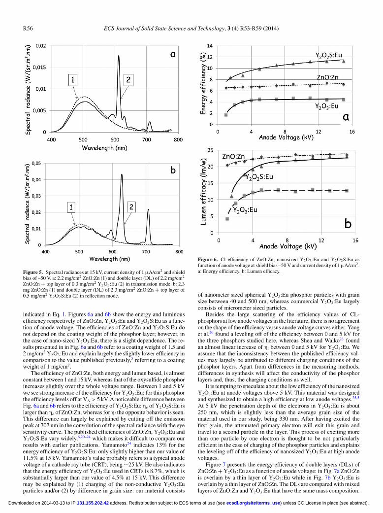
Figure 5. Spectral radiances at 15 kV, current density of 1 μA/cm2 and shieldbias of –50 V. a: 2.2 mg/cm2 ZnO:Zn (1) and double layer (DL) of 2.2 mg/cm2
ZnO:Zn + top layer of 0.3 mg/cm2 Y2O3:Eu (2) in transmission mode. b: 2.3mg ZnO:Zn (1) and double layer (DL) of 2.3 mg/cm2 ZnO:Zn + top layer of0.5 mg/cm2 Y2O2S:Eu (2) in reflection mode.
indicated in Eq. 1. Figures 6a and 6b show the energy and luminousefficiency respectively of ZnO:Zn, Y2O3:Eu and Y2O2S:Eu as a func-tion of anode voltage. The efficiencies of ZnO:Zn and Y2O2S:Eu donot depend on the coating weight of the phosphor layer; however, inthe case of nano-sized Y2O3:Eu, there is a slight dependence. The re-sults presented in in Fig. 6a and 6b refer to a coating weight of 1.5 and2 mg/cm2 Y2O3:Eu and explain largely the slightly lower efficiency incomparison to the value published previously,5 referring to a coatingweight of 1 mg/cm2.
The efficiency of ZnO:Zn, both energy and lumen based, is almostconstant between 1 and 15 kV, whereas that of the oxysulfide phosphorincreases slightly over the whole voltage range. Between 1 and 5 kVwe see strong increase of the efficiency for Y2O3:Eu; for this phosphorthe efficiency levels off at VA > 5 kV. A noticeable difference betweenFig. 6a and 6b refers to the efficiency of Y2O2S:Eu: ηe of Y2O2S:Eu islarger than ηe of ZnO:Zn, whereas for ηl the opposite behavior is seen.This difference can largely be explained by cutting off the emissionpeak at 707 nm in the convolution of the spectral radiance with the eyesensitivity curve. The published efficiencies of ZnO:Zn, Y2O3:Eu andY2O2S:Eu vary widely,6,20–24 which makes it difficult to compare ourresults with earlier publications. Yamamoto24 indicates 13% for theenergy efficiency of Y2O2S:Eu: only slightly higher than our value of11.5% at 15 kV. Yamamoto’s value probably refers to a typical anodevoltage of a cathode ray tube (CRT), being ∼25 kV. He also indicatesthat the energy efficiency of Y2O3:Eu used in CRTs is 8.7%, which issubstantially larger than our value of 4.5% at 15 kV. This differencemay be explained by (1) charging of the non-conductive Y2O3:Euparticles and/or (2) by difference in grain size: our material consists
Figure 6. Cl efficiency of ZnO:Zn, nanosized Y2O3:Eu and Y2O2S:Eu asfunction of anode voltage at shield bias –50 V and current density of 1 μA/cm2.a: Energy efficiency. b: Lumen efficacy.
of nanometer sized spherical Y2O3:Eu phosphor particles with grainsize between 40 and 500 nm, whereas commercial Y2O3:Eu largelyconsists of micrometer sized particles.
Besides the large scattering of the efficiency values of CL-phosphors at low anode voltages in the literature, there is no agreementon the shape of the efficiency versus anode voltage curves either. Yanget al.20 found a leveling off of the efficiency between 0 and 5 kV forthe three phosphors studied here, whereas Shea and Walko23 foundan almost linear increase of ηl between 0 and 5 kV for Y2O3:Eu. Weassume that the inconsistency between the published efficiency val-ues may largely be attributed to different charging conditions of thephosphor layers. Apart from differences in the measuring methods,differences in synthesis will affect the conductivity of the phosphorlayers and, thus, the charging conditions as well.
It is tempting to speculate about the low efficiency of the nanosizedY2O3:Eu at anode voltages above 5 kV. This material was designedand synthesized to obtain a high efficiency at low anode voltages.25,5
At 5 kV the penetration depth of the electrons in Y2O3:Eu is about250 nm, which is slightly less than the average grain size of thematerial used in our study, being 330 nm. After having excited thefirst grain, the attenuated primary electron will exit this grain andtravel to a second particle in the layer. This process of exciting morethan one particle by one electron is thought to be not particularlyefficient in the case of charging of the phosphor particles and explainsthe leveling off of the efficiency of nanosized Y2O3:Eu at high anodevoltages.
Figure 7 presents the energy efficiency of double layers (DLs) ofZnO:Zn + Y2O3:Eu as a function of anode voltage: in Fig. 7a ZnO:Znis overlain by a thin layer of Y2O3:Eu while in Fig. 7b Y2O3:Eu isoverlain by a thin layer of ZnO:Zn. The DLs are compared with mixedlayers of ZnO:Zn and Y2O3:Eu that have the same mass composition.
) unless CC License in place (see abstract). ecsdl.org/site/terms_use address. Redistribution subject to ECS terms of use (see 131.155.202.42Downloaded on 2014-03-13 to IP

ECS Journal of Solid State Science and Technology, 3 (4) R53-R59 (2014) R57
Figure 7. Efficiency of double layers of ZnO:Zn + Y2O3:Eu as a function ofanode voltage, current density of 1 μA/cm2 and shield bias of –50 V. a: DL(double layer): 2.2 mg/cm2 ZnO:Zn overlain by 0.3 mg/cm2 Y2O3:Eu. Theory:calculated efficiency of an ideally mixed layer of 2.2 mg/cm2 ZnO:Zn and0.3 mg/cm2 Y2O3:Eu. b: DL (double layer): 1.5 mg/cm2 Y2O3:Eu overlain by0.4 mg/cm2 ZnO:Zn. Theory: calculated efficiency of an ideally mixed layerof 1.5 mg/cm2 Y2O3:Eu and 0.4 mg/cm2 ZnO:Zn.
Unfortunately, it was not possible to prepare mixed layers of ZnO:Znand Y2O3:Eu by settling without segregation, because of the differencein particle diameter: the larger ZnO:Zn particles settled much fasterthan the nanosized Y2O3:Eu particles. However, the DL-curves shouldbe compared with the curves indicated by “Theory”. These lattercurves refer to the calculated efficiency of ideally mixed layers ofthe two phosphors with the same mass composition as the DLs. Thetheoretical efficiency curves are evaluated as follows:
ηtheor ye = ηe
(1)v(1) + ηe(2)v(2) [6]
where ηe(1) and v(1) are the energy efficiency and the volume fraction
of ZnO:Zn respectively, ηe(2) and v(2) are the corresponding quantities
for Y2O3:Eu; furthermore:
v(2) = 1 − v(1) [7]
The volume fraction is a better quantity to evaluate the weightedaverage of the efficiency than the molar ratio, because the DLs andmixed layers do not form molecular mixed systems.
Figure 8 shows the x-color coordinate (CIE-1931) of DLs ofZnO:Zn + Y2O3:Eu as a function of anode voltage: Fig. 8a refersto the same layers as mentioned in Fig. 7a, while Fig. 8b refers to thesame system as in Fig. 7b. The colors in the reflection (R) and trans-mission (T) modes are different for a DL, both are indicated in thefigures. In Fig. 8 the measured x-color coordinates are compared withthose of an ideally mixed layer. These theoretical x-color coordinatesare evaluated as follows:
xtheor y = ηl(1)v(1)x (1) + ηl
(2)v(2)x (2)
ηl(1)v(1) + ηl
(2)v(2)[8]
Figure 8. x-color coordinate of double layers of ZnO:Zn + Y2O3:Eu in reflec-tion and transmission modes as a function of anode voltage, current density of1 μA/cm2 and shield bias of –50 V. a: R-mode and T-mode of DL: 2.2 mg/cm2
ZnO:Zn overlain by 0.3 mg/cm2 Y2O3:Eu. Theory: x-color coordinate cal-culated for an ideally mixed layer of 2.2 mg/cm2 ZnO:Zn and 0.3 mg/cm2
Y2O3:Eu. b: R-mode and T-mode of DL: 1.5 mg/cm2 Y2O3:Eu overlain by0.4 mg/cm2 ZnO:Zn. Theory: x-color coordinate calculated for an ideallymixed layer of 1.5 mg/cm2 Y2O3:Eu and 0.4 mg/cm2 ZnO:Zn.
where ηl(1) and x(1) are the lumen efficacy and x-color coordinate of
ZnO:Zn respectively, ηl(2) and x(2) are the corresponding quantities
for Y2O3:Eu. Thus, the color coordinate of the ideally mixed layeris obtained by weighing the coordinates of the constituent phosphorswith the product of the volume fraction and the lumen efficacy. Thecolor coordinates (x, y) of CL of ZnO:Zn and Y2O3:Eu are (0.238,0.418) and (0.645,0.348) respectively. Because of the large differencein x-color coordinate (0.407), we limit the considerations on color tothe x-color coordinate only.
First of all the thin Y2O3:Eu layer on top of ZnO:Zn will bediscussed. According to Eq. 5 the effective thickness D of the0.3 mg/cm2 Y2O3:Eu top layer is 0.6 μm. From Fig. 3 it can beconcluded that electrons will not pass this layer at 5 kV; however, at15 kV attenuated primary electrons will penetrate in the ZnO:Zn layer.Figure 7a shows that at low anode voltage the efficiency of a DL ismuch lower than that of the ideal mixture, whereas at VA > 8 kV, theDL has a larger efficiency. It may be concluded that the results repre-sented in Fig. 7a are in line with the penetration model. By depositing anon-conductive layer of Y2O3:Eu on top of ZnO:Zn one might expectcharging and lowering of the efficiency, also at high anode voltage.Since this is not observed, it can be tentatively concluded that theconduction of the bottom ZnO:Zn layer also prevents charging of theY2O3:Eu top layer. In other words, thanks to this discharging effect,enhancement of the efficiency by penetration is observed.
Since the layers comprise of phosphor particles, there are manypin holes in the layers, which implies that some non-attenuated pri-mary electrons will hit the ZnO:Zn layer. This induces a backgroundexcitation of ZnO:Zn at low and high anode voltages. Figure 8a shows
) unless CC License in place (see abstract). ecsdl.org/site/terms_use address. Redistribution subject to ECS terms of use (see 131.155.202.42Downloaded on 2014-03-13 to IP
R58 ECS Journal of Solid State Science and Technology, 3 (4) R53-R59 (2014)
Figure 9. Efficiency of DL and mixed layers of ZnO:Zn + Y2O2S:Eu as afunction of anode voltage, current density of 1 μA/cm2 and shield bias of–50 V. DL: 2.3 mg/cm2 ZnO:Zn overlain by 0.5 mg/cm2 Y2O2S:Eu. The-ory: calculated efficiency of ideally mixed layer of 2.3 mg/cm2 ZnO:Zn and0.5 mg/cm2 Y2O2S:Eu. Mix: measured efficiency of mixed layer of 2.3 mg/cm2
ZnO:Zn and 0.5 mg/cm2 Y2O2S:Eu.
that both the R- and T-mode yield a more red-shifted emission thanthe ideally mixed layer. The x-color coordinate shows a maximumvalue a 5 kV, which can be understood because of the strong increaseof the efficiency of Y2O3:Eu between 0 and 5 kV. At VA > 5 kVa larger fraction of electrons pass the Y2O3:Eu-layer and exciteZnO:Zn, increasing the green component of the luminescence. TheR-mode yields a more red-shifted light than the T-mode, which is tobe expected with a top layer of Y2O3:Eu.
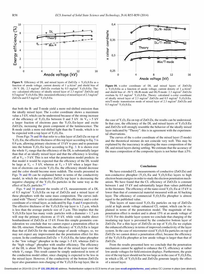
From Figs 7b and 8b that refer to a thin layer of ZnO:Zn on top ofY2O3:Eu, the effective thickness of this top layer according to Eq. 5 is0.9 μm, allowing primary electrons of 15 kV to pass and to penetrateinto the bottom Y2O3:Eu layer according to Fig. 3. It is shown overthe whole VA-range that the efficiency of the DL is substantially largerthan that of an ideally mixed layer and that the efficiency is levelingoff at VA > 5 kV. This is not what the penetration model predicts: inthat model it would be expected that the efficiency of the DL wouldbe large at VA < 5 kV, whereas at VA > 5 kV when a larger frac-tion of electrons can excite Y2O3:Eu, the efficiency should decreaseand the color should become more reddish. The results presented inFigs 7b and 8b can be explained better in terms of the conductivitymodel, in which the conductive ZnO:Zn top layer is decreasing thenegative charging of the Y2O3:Eu particles in the same way as theeffect of In2O3 particles.6,8
Figs. 9 and 10 present the results of CL measurements of a DLof 0.5 mg/cm2 Y2O2S:Eu on top of ZnO:Zn and a mixed layer ofthese phosphors with the same mass composition. The curves indi-cated with “Theory” refer to calculations of the efficiency and x-colorcoordinate of a virtual layer, as indicated by Eqs. 6 and 8 respectively.The effective thickness of the Y2O2S:Eu top layer is 1.2 μm, whichis less than the average particle size of 2 μm. This implies that theY2O2S:Eu layer has many voids: particles with a diameter > 1.7 μmwill stop the primary electrons at 15 kV, while voids enable directbombardment of ZnO:Zn at 15 kV. From this simple geometric con-sideration we conclude that we cannot expect a penetration effect inthis DL-structure. Furthermore, the efficiency of Y2O2S:Eu is largerthan that of ZnO:Zn for the studied range of anode voltages; so, wemay not expect any improvement due the penetration effect for thissystem. In the combination ZnO:Zn + Y2O2S:Eu, the latter phosphoris the “low voltage” phosphor in the range 1–5 kV, whereas ZnO isthe “high voltage” phosphor with smaller efficiency. The efficiencyof the DL is about 30% larger than that of the mixed layer over thewhole VA-range. This result cannot be simply understood in term ofthe conduction model either, since charging is expected to be less inthe mixed layer. However, if the conductivity of the bottom ZnO:Znlayer also guarantees non-charging of the Y2O2S:Eu top layer, like in
Figure 10. x-color coordinate of DL and mixed layers of ZnO:Zn+ Y2O2S:Eu as a function of anode voltage, current density of 1 μA/cm2
and shield bias of –50 V. DL/R-mode and DL/T-mode: 2.3 mg/cm2 ZnO:Znoverlain by 0.5 mg/cm2 Y2O2S:Eu. Theory: calculated x-color coordinateof ideally mixed layer of 2.3 mg/cm2 ZnO:Zn and 0.5 mg/cm2 Y2O2S:Eu.mix/T-mode: transmission mode of mixed layer of 2.3 mg/cm2 ZnO:Zn and0.5 mg/cm2 Y2O2S:Eu.
the case of Y2O3:Eu on top of ZnO:Zn, the results can be understood.In that case, the efficiency of the DL and mixed layers of Y2O2S:Euand ZnO:Zn will strongly resemble the behavior of the ideally mixedlayer indicated by “Theory”: this is in agreement with the experimen-tal observations.
The curves of the x-color coordinate of the mixed layer (T-mode)and the theoretical mixture do not coincide very well. This may beexplained by the inaccuracy in adjusting the mass composition of theDL and mixed layers during settling. We estimate that the accuracy ofthe mass composition of the composite layers is not better than ±5%.
Conclusions
We have extended CL-measurements of conductive (ZnO:Zn) andnon-conductive phosphor (Y2O3:Eu and Y2O2S:Eu) layers to highelectron beam energies in order to study the electron penetration mech-anism. We have found that the CL efficiency of ZnO:Zn is constantbetween 1 and 15 kV and substantially larger than values publishedin the literature. The efficiency of the nano-sized Y2O3:Eu at 15 kV islower than that of commercial material measured with an Al backinglayer. The efficiency of commercial Y2O2S:Eu phosphor is almostequal to the published value.
Thin layers of nano-sized Y2O3:Eu particles on top of ZnO:Znyield at high anode voltage enhanced CL output, which can be ex-plained in terms of the penetration model. The magnitude of thispenetration effect is modest and is about 15% at an anode voltage of15 kV. For this double layer system we conclude that charging of theinsulating top layer is prevented by the conductive bottom layer ofZnO:Zn. For a thin layer of ZnO:Zn on top of Y2O3:Eu we explainthe enhanced efficiency in terms of improved conductivity of the layersystem. In the case of micrometer-sized Y2O2S:Eu particles on top ofZnO:Zn we cannot detect a penetration effect, because the efficiencyof the Y2O2S:Eu phosphor at low anode voltage is larger than that ofZnO:Zn.
From the results presented here we conclude that the penetrationmechanism cannot be applied to enhance the CL efficiency at ratherlow anode voltages for field emission displays. Furthermore, the grainsize of the top layer should not be too large as in the case of Y2O2S:Eu,in which a DL of Y2O2S:Eu and ZnO:Zn generate largely the effectof a mixed layer.
) unless CC License in place (see abstract). ecsdl.org/site/terms_use address. Redistribution subject to ECS terms of use (see 131.155.202.42Downloaded on 2014-03-13 to IP

ECS Journal of Solid State Science and Technology, 3 (4) R53-R59 (2014) R59
Acknowledgments
We are grateful to the EPSRC and the Technology StrategyBoard(TSB) for funding the PURPOSE (TP11/MFE/6/I/AA129F; EP-SRC TS/G000271/1) and CONVERTED (JeS no. TS/1003053/1) pro-grams. We are also grateful to the TSB for funding the CONVERTprogram.
References
1. D. den Engelsen, P. G. Harris, T. G. Ireland, R. Withnall, and J. Silver, SID SymposiumDigest of Technical Papers, 43, 861 (2012).
2. A. M. Morrell, H. B. Law, E. G. Ramberg, and E. W. Herold, “Color TelevisionPicture Tubes”, Academic Press Inc., Orlando (1974), Chapter 8.
3. D. H. Pritchard, “Penetration color screen, color tube, and color television receiver”,US patent 3204143 (1965).
4. J. S. Prener and J. D. Kingsley, J. Electrochem. Soc., 119, 1254 (1972).5. D. den Engelsen, P. G. Harris, T. G. Ireland, R. Withnall, and J. Silver, ECS J. Solid
State Sci. Technol., 2, R201 (2013).6. K. Morimoto and S. Itoh in “Phosphor Handbook”, Chapter 8, Edited by
W. Yen, S. Shionoya, and H. Yamamoto, 2nd ed., CRC-Press, Boca Raton(2007).
7. S.-H. Yang and M. Yokoyama, J. Electr. Mater., 31, 248 (2002).
8. X. G. Xu, J. Chen, S. Z. Deng, N. S. Xu, and J. Lin, J. Vac. Sci. Technol., 28B, 490(2010).
9. X. Hu, X. Huang, Y. Hu, and W. Zhuang, J. Rare Earths, 25, 11 (2007).10. K. Y. Jung and K. H. Han, Electrochem. Solid State Lett., 8, H91 (2005).11. G. Alacon-Flores, M. Aguilar-Frutis, C. Falcony, M. Garcia-Hipolito,
J. J. Araiza-Ibara, and H. J. Herrera-Suarez, J. Vac. Sci. Technol., B24, 1873 (2006).12. H. A. Bethe, Ann. Physik, 5, 325 (1930).13. R. Whiddington, Proc. Roy. Soc. (London), A86, 360 (1912).14. H. M. Terrill, Phys. Rev., 22, 101 (1923).15. R. O. Lane and D. J. Zaffarano, Phys. Rev., 95, 960 (1954).16. C. Feldman, Phys. Rev., 117, 455 (1960).17. T. E. Everhard and P H. Hoff, J. Appl. Phys., 42, 5837 (1971).18. A. F. Makhov, J. D. Kingsley, and J. S. Prener, J. Appl. Phys., 43, 3073 (1972) and
H. Bechtel et al., Philips. J. Res., 50, 433 (1996).19. K. Kanaya and S. Okayama, J. Phys. D: Appl. Phys., 5, 43 (1971).20. S. Yang, F. Zhang, C. Stoffers, S. M. Jacobsen, C. J. Summers, P. N. Yocom, and
S. McClelland, Proc. SPIE., 2408, 194 (1995).21. L. E. Shea, Electrochem. Soc. Interface, Summer, 24 (1998).22. L. E. Shea and R. J. Walko, Proc SPIE, 3636, 105 (1999).23. G. Wakefield, E. Holland, P. J. Dobson, and J. L. Hutchison, Adv. Mater., 13, 1557
(2001).24. H. Yamamoto in “Phosphor Handbook”, Chapter 2.9, Edited by W. Yen, S. Shionoya,
and H. Yamamoto, 2nd ed., CRC-Press, Boca Raton (2007).25. X. Jing, T. Ireland, C. Gibbons, D. Barber, J. Silver, A. Vecht, G. Fern, P. Trogwa,
and D. Morton, J. Electrochem. Soc., 146, 4654 (1999).
) unless CC License in place (see abstract). ecsdl.org/site/terms_use address. Redistribution subject to ECS terms of use (see 131.155.202.42Downloaded on 2014-03-13 to IP
Related Documents