Carrier Thermalization Dynamics in Single Zincblende and Wurtzite InP Nanowires Yuda Wang, Howard E. Jackson, and Leigh M. Smith* Department of Physics, University of Cincinnati, Cincinnati, Ohio 45221-0011, United States Tim Burgess, Suriati Paiman, Qiang Gao, Hark Hoe Tan, and Chennupati Jagadish Department of Electronic Materials Engineering, Research School of Physics and Engineering, The Australian National University, Canberra, Australian Capital Territory 0200, Australia * S Supporting Information ABSTRACT: Using transient Rayleigh scattering (TRS) measurements, we obtain photoexcited carrier thermalization dynamics for both zincblende (ZB) and wurtzite (WZ) InP single nanowires (NW) with picosecond resolution. A phenomenological fitting model based on direct band-to-band transition theory is developed to extract the electron-hole-plasma density and temperature as a function of time from TRS measurements of single nanowires, which have complex valence band structures. We find that the thermalization dynamics of hot carriers depends strongly on material (GaAs NW vs InP NW) and less strongly on crystal structure (ZB vs WZ). The thermalization dynamics of ZB and WZ InP NWs are similar. But a comparison of the thermalization dynamics in ZB and WZ InP NWs with ZB GaAs NWs reveals more than an order of magnitude slower relaxation for the InP NWs. We interpret these results as reflecting their distinctive phonon band structures that lead to different hot phonon effects. Knowledge of hot carrier thermalization dynamics is an essential component for effective incorporation of nanowire materials into electronic devices. KEYWORDS: Nanowire, Zincblende, Wurtzite, Band Structure, Excitation Spectroscopy R ecent dramatic advances in the growth of semiconductor nanowires and their heterostructures have been followed by substantial development of novel devices utilizing these structures 1 including nanoelectronics, 2,3 nanophotonics, 4-6 nanobiochemistry, 7-9 and nanoenergy 10,11 applications. The design of these applications depends critically on knowledge of the relaxation of hot carriers in the semiconductor NWs. Previously, Montazeri et al. 12,13 used time-resolved Rayleigh scattering to obtain detailed information on carrier thermal- ization in GaAs NWs. How these relaxations depend on the NW material, for example, GaAs or InP, or crystal structure, for example, ZB or WZ, is an open question. Here, using a simple analysis of detailed TRS spectra in both ZB and WZ InP NWs, we find that the dynamics in both these crystal structures are dramatically different from what has been observed in ZB GaAs NWs. Although in nature InP exists only in the ZB phase, in nanowire structures both ZB and WZ polytypes can be fabricated with high crystal and optical quality, and homostructures using both polytypes can be made. Though the electronic band structures of ZB and WZ InP nanowires are now well understood, 14-17 there is no information on the thermalization of carriers in WZ InP, and extremely limited information for ZB InP, even in bulk material. 18-21 In this paper, for the first time, we provide a complete picture of the carrier cooling dynamics of both ZB and WZ InP in the picosecond to nanosecond regime at low temperatures analyzing pump-probe transient Rayleigh scattering (TRS) Received: September 29, 2014 Revised: October 28, 2014 Published: November 9, 2014 Letter pubs.acs.org/NanoLett © 2014 American Chemical Society 7153 dx.doi.org/10.1021/nl503747h | Nano Lett. 2014, 14, 7153-7160

Welcome message from author
This document is posted to help you gain knowledge. Please leave a comment to let me know what you think about it! Share it to your friends and learn new things together.
Transcript
Carrier Thermalization Dynamics in Single Zincblende and WurtziteInP NanowiresYuda Wang, Howard E. Jackson, and Leigh M. Smith*
Department of Physics, University of Cincinnati, Cincinnati, Ohio 45221-0011, United States
Tim Burgess, Suriati Paiman, Qiang Gao, Hark Hoe Tan, and Chennupati Jagadish
Department of Electronic Materials Engineering, Research School of Physics and Engineering, The Australian National University,Canberra, Australian Capital Territory 0200, Australia
*S Supporting Information
ABSTRACT: Using transient Rayleigh scattering (TRS) measurements, we obtain photoexcited carrier thermalization dynamicsfor both zincblende (ZB) and wurtzite (WZ) InP single nanowires (NW) with picosecond resolution. A phenomenologicalfitting model based on direct band-to-band transition theory is developed to extract the electron-hole−plasma density andtemperature as a function of time from TRS measurements of single nanowires, which have complex valence band structures. Wefind that the thermalization dynamics of hot carriers depends strongly on material (GaAs NW vs InP NW) and less strongly oncrystal structure (ZB vs WZ). The thermalization dynamics of ZB and WZ InP NWs are similar. But a comparison of thethermalization dynamics in ZB and WZ InP NWs with ZB GaAs NWs reveals more than an order of magnitude slower relaxationfor the InP NWs. We interpret these results as reflecting their distinctive phonon band structures that lead to different hotphonon effects. Knowledge of hot carrier thermalization dynamics is an essential component for effective incorporation ofnanowire materials into electronic devices.KEYWORDS: Nanowire, Zincblende, Wurtzite, Band Structure, Excitation Spectroscopy
Recent dramatic advances in the growth of semiconductornanowires and their heterostructures have been followed
by substantial development of novel devices utilizing thesestructures1 including nanoelectronics,2,3 nanophotonics,4−6
nanobiochemistry,7−9 and nanoenergy10,11 applications. Thedesign of these applications depends critically on knowledge ofthe relaxation of hot carriers in the semiconductor NWs.Previously, Montazeri et al.12,13 used time-resolved Rayleighscattering to obtain detailed information on carrier thermal-ization in GaAs NWs. How these relaxations depend on theNW material, for example, GaAs or InP, or crystal structure, forexample, ZB or WZ, is an open question. Here, using a simpleanalysis of detailed TRS spectra in both ZB and WZ InP NWs,we find that the dynamics in both these crystal structures aredramatically different from what has been observed in ZB GaAsNWs.
Although in nature InP exists only in the ZB phase, innanowire structures both ZB and WZ polytypes can befabricated with high crystal and optical quality, andhomostructures using both polytypes can be made. Thoughthe electronic band structures of ZB and WZ InP nanowires arenow well understood,14−17 there is no information on thethermalization of carriers in WZ InP, and extremely limitedinformation for ZB InP, even in bulk material.18−21
In this paper, for the first time, we provide a complete pictureof the carrier cooling dynamics of both ZB and WZ InP in thepicosecond to nanosecond regime at low temperaturesanalyzing pump−probe transient Rayleigh scattering (TRS)
Received: September 29, 2014Revised: October 28, 2014Published: November 9, 2014
Letter
pubs.acs.org/NanoLett
© 2014 American Chemical Society 7153 dx.doi.org/10.1021/nl503747h | Nano Lett. 2014, 14, 7153−7160
measurements by expanding the analysis of Montazeri et al.12,13
to include complex multiband structures. For instance, in WZInP NWs, relaxation dynamics must include both electronthermalization in a single conduction band, as well as holes inthree separate valence bands: the A (heavy hole), B (lighthole), and C bands,15,16,23 which are separated by energiesdetermined by the spin−orbit and crystal-field interactions.22
To interpret the experimental results, we develop a simpleformalism based on direct band−band theory, which can modelthe changes in the real and imaginary parts of the index ofrefraction when the bands are dynamically occupied by carriers.The many-body effects are included phenomenologically. Weextract the electron−hole density and temperature as a functionof time for each polytype for all bands, as well as their energypositions. We then provide a phenomenological explanation ofthe contrasting dynamics of InP and GaAs NWs by consideringhot phonon effects.TRS Experimental Results and Spectra Fitting Model.
These measurements are performed on single MOCVD grownZB or WZ InP NWs at 10 K. The single phase ZB or WZ InPNWs are nominally 150 nm in diameter. The ZB NWs wereintentionally doped by a low Si-doping concentration ofapproximately 1016 cm−3 (deduced from TRS data analysis),whereas the WZ NWs were undoped. In these TRSexperiments, the polarization of a tunable probe pulse (1.2−2.0 eV) oscillates between parallel and perpendicular to a singlenanowire at 100 kHz using a photoelastic modulator (PEM).Using a balanced detector the backscattered probe pulse ismonitored by a lockin amplifier tuned to the 100 kHz PEMoscillator. This provides the signal which is the polarizedscattering efficiency: R! = R∥ − R⊥. Using a pump pulse (at 2.25eV), carriers are photoexcited into the wire which changes thereal and imaginary part of the index of refraction which in turnchanges the polarized scattering efficiency, R!. Both pump andprobe laser pulses have a width of ∼200 fs. The pump ismodulated on and off by a mechanical chopper at 773 Hz. Bylooking at the change of R! when pump is on and off, weacquired ΔR!, which is a derivative-like structure and is muchsharper than R!. Moreover, the ΔR! is measured at differenttime delays of the probe after the initial pump by adjusting thelength of the time delay line in the probe laser path. With suchan experimental setup, we can measure the relative change ofthe polarized Rayleigh scattering efficiency ΔR!/R! as afunction of both probe energy and probe delay time after thepump.Typical spectra from a single ZB InP NW are shown in
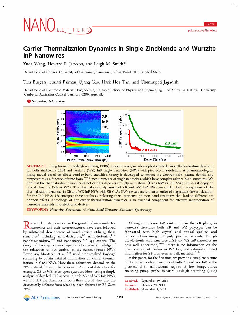
Figure 1b, and the spectra map is plotted as a function of timein Figure 1a. The false color in the TRS map represents thevalue of ΔR!/R!, with red showing positive and blue showingnegative changes in the scattering efficiency R!, where R! is thelinear dichroism (R∥ − R⊥). The derivative-like structurebecomes very sharp at late times when the carrier occupationdensities and temperatures are low, and so the energy positionof the fundamental band to band transition is seen with highaccuracy. The zero crossing point of the TRS spectrum is adirect measure of the energy associated with a direct band-to-band transition. The ZB InP NW band gap Eg is observed at1.42 eV corresponding to an optical transition between thedegenerate light-hole (LH) and heavy hole (HH) bands andthe conduction band, whereas the corresponding transitionbetween the split-off (SO) band to the conduction band isobserved at 110 meV higher energy. Both of the results are inexcellent agreement with previous reports.23−26 The ΔR!/R!
spectral map (Figure 1a) at early times displays a more intenseresponse (larger changes in R!) and exhibits an increasedenergy width and is centered at a higher energy compared tolater times. At very early times (t < 100 ps), the broadeningeffects are strong enough to cause overlapping responsesbetween the higher lying SO-e transition and the lower lyingLH- and HH-e band edge. Perhaps more surprisingly, a veryweak transition is also observed around 1.95 eV, which may beassociated with the Γ−L transition between the top of thevalence band and the conduction band L-valley.To model these light scattering lineshapes, we calculate ΔR!/
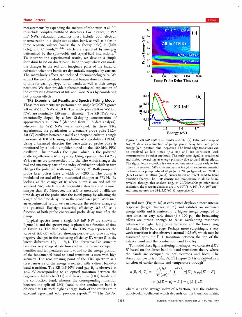
R! based on the direct band-to-band transitions theory wherethe bands are occupied by hot electrons and holes. Theabsorption coefficient ![E, N, T] (Figure 2a) is calculated as afunction of carrier density and temperature through27
∫α ππ
ρ ρ Ε
Ε
= ′ × ′ −
× − − ′ − ′ ′
−E N T c h
n EB E E
f E E f E E
[ , , ](2 )
[ ] [ ]
( [ ] [ ])d
E E
c V
l g u
2 2 3
2 2 3 0
g
where n is the average index of refraction; B is the radiativebimolecular coefficient which depends on the transition matrix
Figure 1. ZB InP NW TRS results and fits. (a) False color map ofΔR!/R! data, as a function of pump−probe delay time and probeenergy (red−positive, blue−negative). The band edge transitions canbe resolved at late times (∼2 ns) and are consistent withmeasurements by other methods. The early time signal is broadenedand shifted toward higher energy primarily due to band filling effects.The signal decay evolution is clear when one moves from early to latetimes. (b) Selected ΔR!/R! vs energy spectra (dots are measurements)for times after pump pulse of 20 ps (red), 200 ps (green), and 2000 ps(blue) as well as fitting (solid) curves based on direct band to bandtransition theory. The EHP density and temperature in all bands arerevealed through this analysis (e.g., at 20/200/2000 ps after initialexcitation, the electron densities are 1 ! 1018/8 ! 1017/8 ! 1016 cm−3
and temperatures are 384/252/60 K, respectively).
Nano Letters Letter
dx.doi.org/10.1021/nl503747h | Nano Lett. 2014, 14, 7153−71607154
element; "i[E] is the 3D density of states in the conduction/valence band; f i[E] = (1/(1 + exp[(E − EF)/(kBT)])) is theFermi−Dirac distribution probability that upper/lower statesinvolved in the transition are occupied by electrons, with thequasi-Fermi energy EF[N, T] related to both the carrier densityN and temperature T; E! is the upper state energy above theconduction band minimum. For n and B, we use the averagevalues from the literature28−35 because only the relative changeof the absorption coefficient is critical, not its absolute value.Using the Kramers−Kronig relation, we transform thecalculated absorption coefficient ![E, N, T] to obtain theindex of refraction n[E, N, T] as a function of carrier densityand temperature. We define the complex refractive index n = n+ ik, where the extinction coefficient k = (#/(4$))!. As shownby Montazeri et al.,13 the line shape ΔR!/R! is the directproduct of a complex phase factor ei% containing NWgeometrical information and the change of the complex indexof refraction Δn = Δn + iΔk. We therefore can write
Δ Δ Δα λπ
θ Δ λπ θ Δα
′′ = +
= −
θ⎜ ⎟⎛⎝
⎞⎠
{ }R
RAe n i
A n
4
cos[ ]4
sin[ ]
i
where A is an overall arbitrary amplitude factor. In Figure 2 weshow the resulting coefficients !, n, Δ!, Δn and ΔR!/R! for theHH-e optical transition corresponding to fits of the ZB InPTRS spectra at various times.The final fitting curve is simply the superposition of each
ΔR!/R! curve for transitions from each of the three valencebands to the conduction band using the following assumptions:(1) the temperature of the electrons and holes are thesame36−38 (i.e., they are thermalized with each other throughrapid (<1 ps) carrier−carrier scattering after initial excitation);(2) the sum of the hole densities in all 3 valence bands (HH,LH, SO for ZB/A, B, C for WZ) equals the density of electronsin the conduction band (i.e., charge neutrality is assumed); (3)the background density without pump excitation is 1015 cm−3
(i.e., the probe pulse itself excites a few carriers), which meansthat separate quasi-Fermi energies are defined for each bandeven if we assume the pump-excited holes are in thermalequilibrium between various hole bands; (4) the background
temperature for these measurements is 10 K; (5) the amplitudefactor A and bimolecular coefficient B are the same if similarelectronic selection rules39,40 exist among different transitions(the HH-e transition intensity dominates over LH-e or SO-e inZB InP, because the HH mass dominates23,41 where density ofstates effective mass is one of the prefactors of n and !, whichturn out to be the component of the modeled ΔR!/R!); (6)band-gap-renormalization (BGR) effects42,43 occur due to themany-body-effects of the EHP and are treated as a free time-dependent fitting parameter causing a rigid shift in the bandgap.To fit the entire TRS spectra as a function of time, we
optimize all the parameters by running iteration cycles. Withineach cycle, we keep time-independent parameters fixed buttune and optimize time-dependent parameters to acquire thebest fits for all the spectra. Those time-dependent parametersare carrier densities, common carrier temperatures and theBGR coefficients. The time-independent parameters are theband gap, SO split-off energy, amplitude factors, and NWgeometry phase factor as well as the background density andtemperature. After one cycle is finished, we adjust time-independent parameters slightly and start another iterationcycle. By continually comparing the fitting results from differentiterations, we finally acquire the optimized time-independentparameters as well as the corresponding time-dependentparameters. The results of these fits are selectively shown atseveral times after the pump pulse in Figure 1b. The fitted bandgap for ZB InP NW is 1.419 ± 0.001 eV and the split-off bandis 0.108 ± 0.001 eV below the top of the valence band. Thesetransition energies agree well with previous reports23−26 anddirect observations of the derivative structures at late times(Figure 1a). The fitted phase factor result indicates thediameter of the NW is approximately 160 nm based on therelation between phase factor and nanowire diameter.12 Inanalyzing the fits to the ΔR!/R! spectrum, we find that theintensity is primarily related to the hot carrier concentration,whereas the spectral width is primarily related to the hot carriertemperature and band filling. As a result of these effects, thescattering lineshapes can overlap strongly at early times whenboth the density and temperatures are high. This overlap showsup, for instance, for the ZB InP Eg + Δso transition near 100 pswhere both the intensity and energy appear to drop. This
Figure 2. (a) and (b) Solid lines show the calculated absorption coefficient ![E] and index of refraction n[E] as a function of energy at differenttimes (20, 200, and 2000 ps shown as red, green and blue respectively) after initial pump-excitation obtained from the spectral line shape fittingdisplayed in Figure 1b. The background !o[E] and no[E] (dashed) are calculated with no pump-photoexcitation but only probe-excitation (i.e., logNo = 1015 cm−3, To = 10 K). (c) and (d) Change of the absorption coefficient Δ![E] and index of refraction Δn[E] at different times after initialpump with respect to background !o and no. (e) The final Rayleigh scattering efficiency ((ΔR!)/R!) ∝ (Δn + iΔ!(#/(4$))) ei% is represented as adirect product of the complex index of refraction and complex phase factor related to the nanowire geometry.
Nano Letters Letter
dx.doi.org/10.1021/nl503747h | Nano Lett. 2014, 14, 7153−71607155
structure results from the superposition of the spectrallineshapes at Eg and Eg + Δso. At the earliest times, the bandgap renormalization tend to reduce the band gap slightly butthe strong band filling effects eventually cause the ΔR!/R!structure move to higher energy. Due to the small electroneffective mass compared to holes, this band filling effect isdominated by the pump-modulated electron distribution in theconduction band.Similar TRS measurements have been carried out on a single
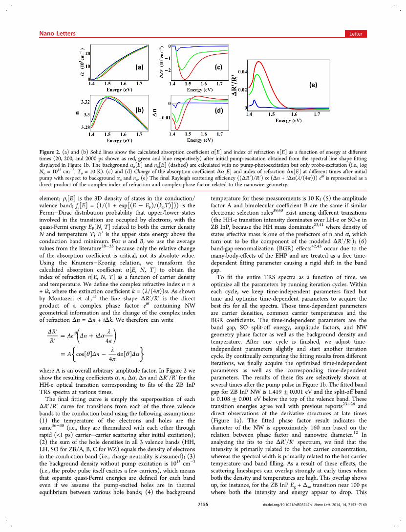
MOCVD grown 150 nm diameter undoped WZ InP NW atpump excitation intensity 4 ! 105 kW cm−2, as displayed inFigure 3a. By looking at the zero point of the derivative-like
structure at late times, the WZ InP NW Eg is observed at ∼1.49eV which is the energy of the optical transition between the Avalence band and the conduction band, whereas the B valenceband to conduction band transition is observed ∼30 meVhigher in energy, and the C valence band to conduction bandtransition is seen ∼160 meV higher in energy. At a larger pumpexcitation intensity 2 ! 106 kW cm−2, the A and B valence bandto second conduction band can be resolved at 1.74 and 1.77 eV(see Supporting Information Figure S1). These results are inexcellent agreement with recent reports.15,16,22,44 Similar bandfilling behavior to that observed in ZB InP is also seen in theWZ InP NWs. We use the same fitting model based on directband-to-band transition theory to extract the WZ InP NW EHPdensity and temperature as a function of time. One differencefor the WZ InP TRS data fitting model is that the A−etransition intensity is extremely weak compared with B−e orC−e. The reason for this is that the A−e transition is onlyallowed for an electric-field polarized perpendicular to the WZInP c axis (NW long-axis), but this field is suppressed by the
dielectric contrast between the NW (150 nm diameter muchsmaller than the laser wavelength ∼800 nm) and thesurrounding media (vacuum). The results of these fits areshown at several times after the pump pulse in Figure 3b. Thefitted A, B, C-valence band to conduction band energies for WZInP are 1.485 ± 0.005 eV, 1.523 ± 0.005 eV, and 1.654 ± 0.005eV, respectively, which agree well with previous reports15,16 anddirect observations of the derivative structures at late times(Figure 3a). The fitted phase factor result gives an approximateNW diameter of 160 nm based on the relation between phasefactor and nanowire diameter;12 the average diameter of NWsmeasured by TEM for this growth is about 150 nm.22
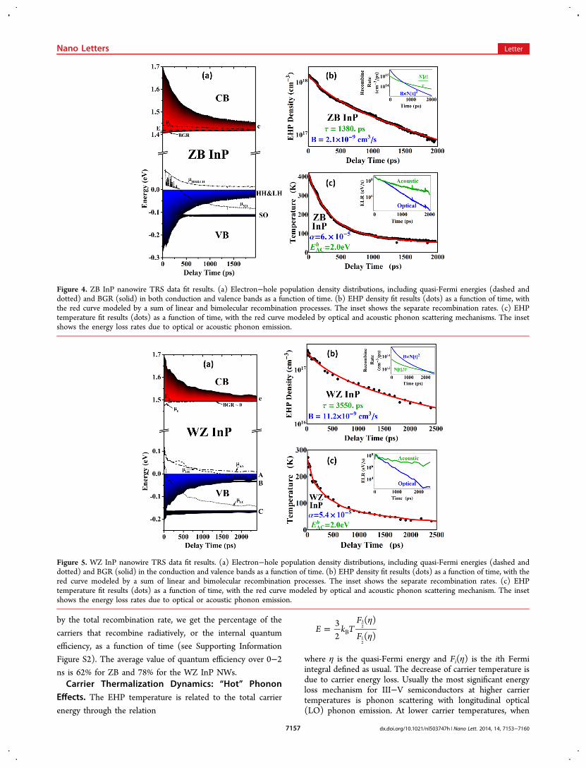
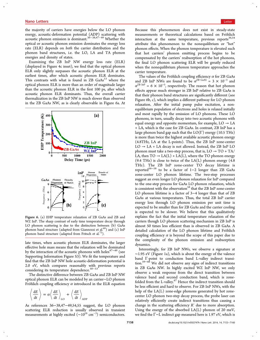
EHP Density and Temperature Relaxation. With thedynamics of carrier density and temperature obtained from thefits to the TRS spectra, we can now plot the carrier populationdensity distribution versus time for all conduction and valencebands. These are displayed in Figure 4a for ZB InP and Figure5a for WZ InP. We assume that the background carrier densitywithout pump excitation is 1015 cm−3, so at late times when thecarrier temperature is low, the occupation of the SO (for ZB)or B, C (for WZ) valence bands is still observable. For the samereason, the quasi-Fermi energy for each band is computedindividually from carrier density and temperature (with Fermi−Dirac distribution and 3D density of states) in spite of theassumption that pump excited holes in different hole bands arein thermal equilibrium, which means each hole band’s quasi-Fermi energies should be equal. The fact that the quasi-Fermienergy is usually within kBT of the band edge supports ourassumption that the pump-excited carriers in the NWs are adegenerate EHP, and thus, we can ignore excitonic effects.The EHP density and temperature obtained from these fits as
a function of time are plotted in Figures 4b, c and 5b, c. Thecarrier density and temperature of the ZB InP NW is 1.5 ! 1018
cm−3 and 400 K at t = 0, which relaxes to 7.5 ! 1016 cm−3 and70 K by 2 ns. In contrast, the carrier density and temperature ofthe WZ InP NW is 2 ! 1017 cm−3 and 270 K at t = 0 whichrelaxes to 2 ! 1016 cm−3 and 50 K by 2 ns. The difference of theinitial carrier density and temperature reflects the fact that thepump excitation intensity for the ZB NW was 1.2 ! 106 kWcm−2, whereas the WZ NW intensity was lower at 4 ! 105 kWcm−2. The larger excitation intensity is also reflected by the factthat the ZB electron quasi-Fermi energy is above theconduction band edge at the earliest times, whereas the WZelectron quasi-Fermi energy is close to the conduction bandedge. Similarly, the BGR of ZB InP NW is larger than WZ InPdue to the higher EHP density.To model the dynamics of the EHP carrier density, we
include both linear (nonradiative) and bimolecular (radiative)recombination processes ignoring the background density fromeither unintentional doping or probe excitation. We describethe decay of the EHP density based on the sum of linear andbimolecular recombination by dN/dt = −N/& − BN2 andobtain the nonradiative lifetime & and bimolecular coefficient Bfor both ZB and WZ InP NWs. For the ZB InP NWs, & ∼ 1.4ns and B ∼ 2 ! 10−9 cm−3 s−1; whereas for the WZ InP NWs, &∼ 3.4 ns and B ∼ 11 ! 10−9 cm−3 s−1. These values comparereasonably well with previous reports,29−35,45,46 taking intoaccount that both parameters are strongly affected by samplequality, temperature, and excitation carrier density. With theknowledge of & and B, the density loss rate through bothrecombination mechanisms can be extracted. The values of thedifferent loss rates as a function of time are plotted in the insetsof Figures 4b and 5b. Dividing the radiative recombination rate
Figure 3. WZ InP nanowire TRS results and fits: (a) False color mapof ΔR!/R! data as a function of pump−probe delay time and probeenergy (red−positive, blue−negative), (b) Selected ΔR!/R! spectra(dots are measurements) as well as fitted (solid) curves based ondirect band-to-band transition theory.
Nano Letters Letter
dx.doi.org/10.1021/nl503747h | Nano Lett. 2014, 14, 7153−71607156
by the total recombination rate, we get the percentage of thecarriers that recombine radiatively, or the internal quantumefficiency, as a function of time (see Supporting InformationFigure S2). The average value of quantum efficiency over 0−2ns is 62% for ZB and 78% for the WZ InP NWs.Carrier Thermalization Dynamics: “Hot” Phonon
Effects. The EHP temperature is related to the total carrierenergy through the relation
ηη=E k T
F
F32
( )
( )B
32
12
where ' is the quasi-Fermi energy and Fi(') is the ith Fermiintegral defined as usual. The decrease of carrier temperature isdue to carrier energy loss. Usually the most significant energyloss mechanism for III−V semiconductors at higher carriertemperatures is phonon scattering with longitudinal optical(LO) phonon emission. At lower carrier temperatures, when
Figure 4. ZB InP nanowire TRS data fit results. (a) Electron−hole population density distributions, including quasi-Fermi energies (dashed anddotted) and BGR (solid) in both conduction and valence bands as a function of time. (b) EHP density fit results (dots) as a function of time, withthe red curve modeled by a sum of linear and bimolecular recombination processes. The inset shows the separate recombination rates. (c) EHPtemperature fit results (dots) as a function of time, with the red curve modeled by optical and acoustic phonon scattering mechanisms. The insetshows the energy loss rates due to optical or acoustic phonon emission.
Figure 5. WZ InP nanowire TRS data fit results. (a) Electron−hole population density distributions, including quasi-Fermi energies (dashed anddotted) and BGR (solid) in the conduction and valence bands as a function of time. (b) EHP density fit results (dots) as a function of time, with thered curve modeled by a sum of linear and bimolecular recombination processes. The inset shows the separate recombination rates. (c) EHPtemperature fit results (dots) as a function of time, with the red curve modeled by optical and acoustic phonon scattering mechanism. The insetshows the energy loss rates due to optical or acoustic phonon emission.
Nano Letters Letter
dx.doi.org/10.1021/nl503747h | Nano Lett. 2014, 14, 7153−71607157
the majority of carriers have energies below the LO phononenergy, acoustic-deformation potential (ADP) scattering withacoustic phonon emission is dominant.36−38,47−49 Whether theoptical or acoustic phonon emission dominates the energy lossrate (ELR) depends on both the carrier distribution and thephonon band structures, i.e. the LO, LA and TA phononenergies and density of states.Examining the ZB InP NW energy loss rate (ELR)
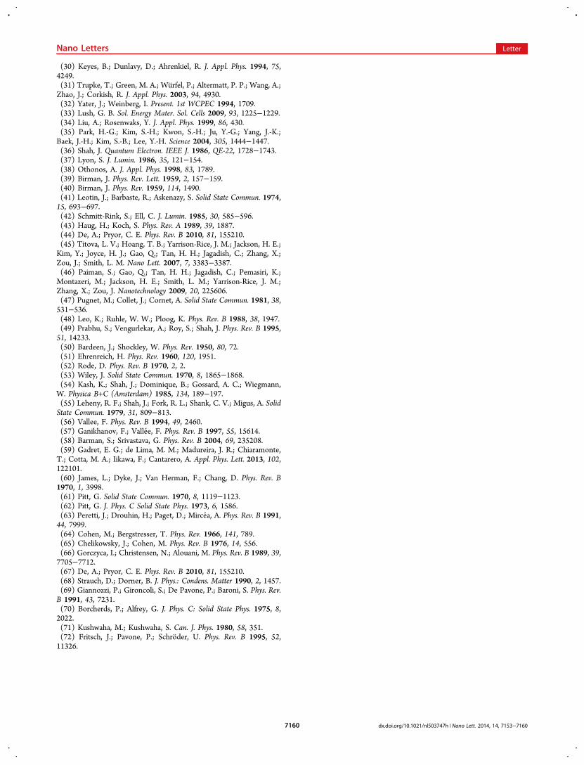
(displayed in Figure 4c inset), we find that the optical phononELR only slightly surpasses the acoustic phonon ELR at theearliest times, after which acoustic phonon ELR dominates.This contrasts with what is found in ZB GaAs13 where theoptical phonon ELR is more than an order of magnitude largerthan the acoustic phonon ELR in the first 100 ps, after whichacoustic phonon ELR dominants. Thus, the overall carrierthermalization in the ZB InP NW is much slower than observedin the ZB GaAs NW, as is clearly observable in Figure 6a. At
late times, when acoustic phonon ELR dominates, the largereffective hole mass means that the relaxation will be dominatedby the interaction of the acoustic phonons with holes47−49 (seeSupporting Information Figure S3). We fit the temperature andfind that the ZB InP NW hole acoustic-deformation potential is2.0 eV, which compares reasonably with previous reportsconsidering its temperature dependence.50−53
The distinctive difference between ZB GaAs and ZB InP NWoptical phonon ELR can be modeled by an carrier−LO phononFrohlich coupling efficiency ! introduced in the ELR equation
α= +Et
Et
Et
dd
dd
ddLO ADP
As references 36−38,47−49,54,55 suggest, the LO phononscattering ELR reduction is usually observed in transientmeasurements at highly excited (∼1018 cm−3) semiconductors.
Because this phenomenon does not exist in steady-statemeasurements or theoretical calculations based on Frohlichinteraction at the same temperature, previous reports36,54
attribute this phenomenon to the nonequilibrium or “hot”phonon effects. When the phonon temperature is elevated suchthat hot carriers’ phonon emitting process begins to becompensated by the carriers’ reabsorption of the hot phonons,the final LO phonon scattering ELR will be greatly reducedwhen the nonequilibrium phonon temperature approaches thecarrier temperature.The values of the Frohlich coupling efficiency ! for ZB GaAs
and ZB InP NWs are found to be !ZB GaAS = 3 ! 10−3 and!ZB InP = 6 ! 10−5, respectively. The reason that hot phononeffects appear much stronger in ZB InP relative to ZB GaAs isthat their phonon band structures are significantly different (seeFigure 6b, c), which implies a different pathway for LO phononrelaxation. After the initial pump pulse excitation, a non-equilibrium population of electrons and holes is relaxed initiallyand most rapidly by the emission of LO phonons. These LOphonons, in turn, usually decay into two acoustic phonons withequal energy and opposite momentum, for example, LO ! LA+ LA, which is the case for ZB GaAs. In contrast, ZB InP has alarge phonon band gap such that the LO(Γ) energy (10.5 THz)is more than twice the highest available acoustic phonon energy(4.8THz, LA at the L-points). Thus, the ZB InP zone-centerLO ! LA + LA decay is not allowed. Instead, the ZB InP LOphonon must take a two-step process, that is, LO! TO + TA/LA, then TO! LA(L) + LA(L), where the TO phonon energy(9.4 THz) is close to twice of the LA(L) phonon energy (4.8THz). The ZB InP zone-center TO decay lifetime isreported56−58 to be a factor of 1−2 longer than ZB GaAszone-center LO phonon lifetime. The two-step processessuggest an even longer LO phonon relaxation for InP comparedto the one-step process for GaAs LO phonon relaxation, whichis consistent with the observation58 that the ZB InP zone-centerLO phonon lifetime is a factor of 3−4 longer than that of ZBGaAs at various temperatures. Thus, the total ZB InP carrierenergy loss through LO phonon emission per unit time isexpected to be smaller than for ZB GaAs and the carrier coolingis expected to be slower. We believe that this qualitativelyexplains the fact that the initial temperature relaxation of thecarriers though LO phonon scattering mechanism in ZB InP isalmost 50 times less efficient than is observed in ZB GaAs. Adetailed calculation of the LO phonon lifetime and Frohlichcoupling efficiency ! is beyond the scope of this paper due tothe complexity of the phonon emission and reabsorptiondynamics.Interestingly, for ZB InP NWs, we observe a signature at
∼1.95 eV (Figure 1a), which is about the energy of the valenceband Γ-point to conduction band L-valley indirect transi-tion.59−66 We did not observe any signs of indirect transitionsin ZB GaAs NW. In highly excited WZ InP NW, we onlyobserve a weak response from the direct transition betweenvalence band and second conduction band, which is zone-folded from the L-valley.67 Hence the indirect transition shouldbe less efficient and hard to observe. For ZB InP NWs, with thehelp of the LA(L) zone-edge phonons generated by hot zone-center LO phonon two-step decay process, the probe laser canrelatively efficiently create indirect transitions thus causing achange in the scattering efficiency R! due to more absorption.Using the energy of the absorbed LA(L) phonon of 20 meV,we find the Γ−L indirect gap measured here is 1.97 eV, which is
Figure 6. (a) EHP temperature relaxation of ZB GaAs and ZB andWZ InP. The sharp contrast of early time temperature decay throughLO phonon scattering is due to the distinction between (b) GaAsphonon band structure (adapted from Giannozzi et al.69) and (c) InPphonon band structure (adapted from Fritsch et al.72).
Nano Letters Letter
dx.doi.org/10.1021/nl503747h | Nano Lett. 2014, 14, 7153−71607158
in the range of previous reports 1.94−2.2 eV at lowtemperatures.59−66
Looking at the WZ InP NW ELR (Figure 5c inset), we findthat the ratio of the initial ELR by LO and acoustic phononscattering is similar to ZB InP NW, but still much less than thatof ZB GaAs NWs. This is reflected by the value of the WZ InPNWs Frohlich coupling efficiency !WZ InP = 5.4 ! 10−5. TheWZ InP hole acoustic-deformation potential, fitted through asimilar process as ZB InP, is found to be ∼2 eV, which agreeswith bulk ZB InP results.50−53 Although there is no directreport of WZ InP LO phonon decay lifetimes eitherexperimentally (recall that WZ InP does not exist in bulkform) or theoretically, we can still interpret this result using thesame phenomenological decay channel framework as detailedabove for ZB InP. For instance, the WZ InP phonon bandstructures at Γ−A dispersion along [0001] can be roughlyapproximated59 by folding the ZB InP Γ−L of the phononband structure along [111]. The phonon states are nowdistributed closer to the zone-center, but the top of the acousticbranches should be still at exactly the same energy as ZB InPand the dispersion of LO/TO branches would not change dueto the flat dispersion nature of the optical branches. Hence, thedirect LO ! LA + LA process is still not allowed for WZ InPand a similar two-step process like that of ZB InP is required.For that reason, we would expect a similar hot phonon effectfor WZ InP NW and thus a similarly slow thermalizationprocess as in ZB InP NW, in agreement with our observations.Conclusions. Using time-resolved Rayleigh scattering, we
have directly measured the density and temperature relaxationof optically excited electron−hole plasma in single ZB and WZInP nanowires. We demonstrate that a simple analysistechnique enables the extraction of the electron and holedensity and temperature in complex multiband materials.Compared with similar measurements of ZB GaAs nanowires,we find that the thermalization time of the EHP is nearly 50times longer in ZB InP nanowires. This slower thermalization islikely caused by the substantially different phonon bandstructure of InP compared to GaAs, which inhibits the directrelaxation of optical to acoustic phonons. Both ZB InPnanowires and WZ InP nanowires have similar thermalizationdynamics. Information on the dependence of carrier thermal-ization dynamics in different materials and nanostructures is anessential component for the design of high efficiency nanowiredevices.
! ASSOCIATED CONTENT*S Supporting InformationAn additional WZ InP TRS spectrum is provided, showingexcitations to the second conduction band, as well as moredetail on the ELR for electron and hole bands separately. Thismaterial is available free of charge via the Internet at http://pubs.acs.org.
! AUTHOR INFORMATIONCorresponding Author*E-mail: [email protected] authors declare no competing financial interest.
! ACKNOWLEDGMENTSWe acknowledge the financial support of the National ScienceFoundation through grants DMR-1105362, 1105121, and
ECCS-1100489 and the Australian Research Council. TheAustralian National Fabrication Facility is acknowledged foraccess to the growth facilities used in this research.
! REFERENCES(1) Yang, P.; Yan, R.; Fardy, M. Nano Lett. 2010, 10, 1529−1536.(2) Cui, Y.; Lieber, C. M. Science 2001, 291, 851−853.(3) Huang, Y.; Duan, X.; Cui, Y.; Lauhon, L. J.; Kim, K. H.; Lieber, C.M. Science 2001, 294, 1313−1317.(4) Huang, Y.; Duan, X.; Lieber, C. M. Small 2005, 1, 142−147.(5) Qian, F.; Gradecak, S.; Li, Y.; Wen, C.-Y.; Lieber, C. M. NanoLett. 2005, 5, 2287−2291.(6) Minot, E. D.; Kelkensberg, F.; van Kouwen, M.; van Dam, J. a;Kouwenhoven, L. P.; Zwiller, V.; Borgstrom, M. T.; Wunnicke, O.;Verheijen, M. a; Bakkers, E. P. a M. Nano Lett. 2007, 7, 367−371.(7) Cui, Y.; Wei, Q.; Park, H.; Lieber, C. M. Science 2001, 293,1289−1292.(8) Zheng, G.; Patolsky, F.; Cui, Y.; Wang, W. U.; Lieber, C. M. Nat.Biotechnol. 2005, 23, 1294−1301.(9) Robinson, J. T.; Jorgolli, M.; Shalek, A. K.; Yoon, M.-H.; Gertner,R. S.; Park, H. Nat. Nanotechnol. 2012, 7, 180−184.(10) Chan, C. K.; Peng, H.; Liu, G.; McIlwrath, K.; Zhang, X. F.;Huggins, R. a; Cui, Y. Nat. Nanotechnol. 2008, 3, 31−35.(11) Hochbaum, A. I.; Yang, P. Chem. Rev. 2010, 110, 527−546.(12) Montazeri, M.; Wade, A.; Fickenscher, M.; Jackson, H. E.;Smith, L. M.; Yarrison-Rice, J. M.; Gao, Q.; Tan, H. H.; Jagadish, C.Nano Lett. 2011, 11, 4329−4336.(13) Montazeri, M.; Jackson, H. E.; Smith, L. M.; Yarrison-Rice, J.M.; Kang, J.-H.; Gao, Q.; Tan, H. H.; Jagadish, C. Nano Lett. 2012, 12,5389−5395.(14) Mishra, A.; Titova, L. V.; Hoang, T. B.; Jackson, H. E.; Smith, L.M.; Yarrison-Rice, J. M.; Kim, Y.; Joyce, H. J.; Gao, Q.; Tan, H. H.;Jagadish, C. Appl. Phys. Lett. 2007, 91, 263104.(15) Perera, S.; Pemasiri, K.; Fickenscher, M. a.; Jackson, H. E.;Smith, L. M.; Yarrison-Rice, J.; Paiman, S.; Gao, Q.; Tan, H. H.;Jagadish, C. Appl. Phys. Lett. 2010, 97, 023106.(16) Gadret, E. G.; Dias, G. O.; Dacal, L. C. O.; de Lima, M. M.;Ruffo, C. V. R. S.; Iikawa, F.; Brasil, M. J. S. P.; Chiaramonte, T.;Cotta, M. A.; Tizei, L. H. G.; Ugarte, D.; Cantarero, A. Phys. Rev. B2010, 82, 125327.(17) Pemasiri, K.; Montazeri, M.; Gass, R.; Smith, L. M.; Jackson, H.E.; Yarrison-Rice, J. M.; Paiman, S.; Gao, Q.; Tan, H. H.; Jagadish, C.;Zhang, X.; Zou, J. Nano 2009, 9, 648.(18) Rota, L.; Lugli, P.; Elsaesser, T.; Shah, J. Phys. Rev. B: Condens.Matter Mater. Phys. 1993, 47, 4226−4237.(19) Hohenester, U.; Supancic, P.; Kocevar, P.; Zhou, X.; Kutt, W.;Kurz, H. Phys. Rev. B: Condens. Matter Mater. Phys. 1993, 47, 13233−13245.(20) Yong, C. K.; Wong-Leung, J.; Joyce, H. J.; Lloyd-Hughes, J.;Gao, Q.; Tan, H. H.; Jagadish, C.; Johnston, M. B.; Herz, L. M. NanoLett. 2013, 13, 4280−4287.(21) Clady, R.; Tayebjee, M. J. Y.; Aliberti, P.; Konig, D.; Clady, R.;John, N.; Daukes, E.; Conibeer, G. J.; Schmidt, T. W.; Green, M. A.Prog. Photovolt Res. Appl. 2012, 20, 82−92.(22) Perera, S.; Shi, T.; Fickenscher, M. A.; Jackson, H. E.; Smith, L.M.; Yarrison-Rice, J. M.; Paiman, S.; Gao, Q.; Tan, H. H.; Jagadish, C.Nano Lett. 2013, 13, 5367−5372.(23) Vurgaftman, I.; Meyer, J. R.; Ram-Mohan, L. R. J. Appl. Phys.2001, 89, 5815.(24) Rochon, P.; Fortin, E. Phys. Rev. B 1975, 12, 5803.(25) Camassel, J.; Merle, P.; Bayo, L.; Mathieu, H. Phys. Rev. B 1980,22, 2020−2024.(26) Mathieu, H.; Chen, Y.; Camassel, J. Phys. Rev. B 1985, 32, 4042.(27) Lasher, G.; Stern, F. Phys. Rev. 1964, 133, A553.(28) Adachi, S. J. Appl. Phys. 1989, 66, 6030.(29) Rosenwaks, Y.; Shapira, Y.; Huppert, D. Phys. Rev. B 1992, 45,9108.
Nano Letters Letter
dx.doi.org/10.1021/nl503747h | Nano Lett. 2014, 14, 7153−71607159
(30) Keyes, B.; Dunlavy, D.; Ahrenkiel, R. J. Appl. Phys. 1994, 75,4249.(31) Trupke, T.; Green, M. A.; Wurfel, P.; Altermatt, P. P.; Wang, A.;Zhao, J.; Corkish, R. J. Appl. Phys. 2003, 94, 4930.(32) Yater, J.; Weinberg, I. Present. 1st WCPEC 1994, 1709.(33) Lush, G. B. Sol. Energy Mater. Sol. Cells 2009, 93, 1225−1229.(34) Liu, A.; Rosenwaks, Y. J. Appl. Phys. 1999, 86, 430.(35) Park, H.-G.; Kim, S.-H.; Kwon, S.-H.; Ju, Y.-G.; Yang, J.-K.;Baek, J.-H.; Kim, S.-B.; Lee, Y.-H. Science 2004, 305, 1444−1447.(36) Shah, J. Quantum Electron. IEEE J. 1986, QE-22, 1728−1743.(37) Lyon, S. J. Lumin. 1986, 35, 121−154.(38) Othonos, A. J. Appl. Phys. 1998, 83, 1789.(39) Birman, J. Phys. Rev. Lett. 1959, 2, 157−159.(40) Birman, J. Phys. Rev. 1959, 114, 1490.(41) Leotin, J.; Barbaste, R.; Askenazy, S. Solid State Commun. 1974,15, 693−697.(42) Schmitt-Rink, S.; Ell, C. J. Lumin. 1985, 30, 585−596.(43) Haug, H.; Koch, S. Phys. Rev. A 1989, 39, 1887.(44) De, A.; Pryor, C. E. Phys. Rev. B 2010, 81, 155210.(45) Titova, L. V.; Hoang, T. B.; Yarrison-Rice, J. M.; Jackson, H. E.;Kim, Y.; Joyce, H. J.; Gao, Q.; Tan, H. H.; Jagadish, C.; Zhang, X.;Zou, J.; Smith, L. M. Nano Lett. 2007, 7, 3383−3387.(46) Paiman, S.; Gao, Q.; Tan, H. H.; Jagadish, C.; Pemasiri, K.;Montazeri, M.; Jackson, H. E.; Smith, L. M.; Yarrison-Rice, J. M.;Zhang, X.; Zou, J. Nanotechnology 2009, 20, 225606.(47) Pugnet, M.; Collet, J.; Cornet, A. Solid State Commun. 1981, 38,531−536.(48) Leo, K.; Ruhle, W. W.; Ploog, K. Phys. Rev. B 1988, 38, 1947.(49) Prabhu, S.; Vengurlekar, A.; Roy, S.; Shah, J. Phys. Rev. B 1995,51, 14233.(50) Bardeen, J.; Shockley, W. Phys. Rev. 1950, 80, 72.(51) Ehrenreich, H. Phys. Rev. 1960, 120, 1951.(52) Rode, D. Phys. Rev. B 1970, 2, 2.(53) Wiley, J. Solid State Commun. 1970, 8, 1865−1868.(54) Kash, K.; Shah, J.; Dominique, B.; Gossard, A. C.; Wiegmann,W. Physica B+C (Amsterdam) 1985, 134, 189−197.(55) Leheny, R. F.; Shah, J.; Fork, R. L.; Shank, C. V.; Migus, A. SolidState Commun. 1979, 31, 809−813.(56) Vallee, F. Phys. Rev. B 1994, 49, 2460.(57) Ganikhanov, F.; Vallee, F. Phys. Rev. B 1997, 55, 15614.(58) Barman, S.; Srivastava, G. Phys. Rev. B 2004, 69, 235208.(59) Gadret, E. G.; de Lima, M. M.; Madureira, J. R.; Chiaramonte,T.; Cotta, M. A.; Iikawa, F.; Cantarero, A. Appl. Phys. Lett. 2013, 102,122101.(60) James, L.; Dyke, J.; Van Herman, F.; Chang, D. Phys. Rev. B1970, 1, 3998.(61) Pitt, G. Solid State Commun. 1970, 8, 1119−1123.(62) Pitt, G. J. Phys. C Solid State Phys. 1973, 6, 1586.(63) Peretti, J.; Drouhin, H.; Paget, D.; Mircea, A. Phys. Rev. B 1991,44, 7999.(64) Cohen, M.; Bergstresser, T. Phys. Rev. 1966, 141, 789.(65) Chelikowsky, J.; Cohen, M. Phys. Rev. B 1976, 14, 556.(66) Gorczyca, I.; Christensen, N.; Alouani, M. Phys. Rev. B 1989, 39,7705−7712.(67) De, A.; Pryor, C. E. Phys. Rev. B 2010, 81, 155210.(68) Strauch, D.; Dorner, B. J. Phys.: Condens. Matter 1990, 2, 1457.(69) Giannozzi, P.; Gironcoli, S.; De Pavone, P.; Baroni, S. Phys. Rev.B 1991, 43, 7231.(70) Borcherds, P.; Alfrey, G. J. Phys. C: Solid State Phys. 1975, 8,2022.(71) Kushwaha, M.; Kushwaha, S. Can. J. Phys. 1980, 58, 351.(72) Fritsch, J.; Pavone, P.; Schroder, U. Phys. Rev. B 1995, 52,11326.
Nano Letters Letter
dx.doi.org/10.1021/nl503747h | Nano Lett. 2014, 14, 7153−71607160
Related Documents