Carbon nanotube micro-electrodes for neuronal interfacing E. Ben-Jacob a and Y. Hanein * b DOI: 10.1039/b805878b This article highlights our recent progress in developing carbon nanotube based electrodes for neurochip applications. By integrating carbon nanotube growth with standard micro- fabrication techniques we have realized novel carbon nanotube based micro-electrode arrays for neuronal interfacing and network engineering. The novel electrodes possess a unique set of properties that make them a promising platform for future neuronal interfacing applications. In particular, carbon nanotube electrodes may potentially be used for neuro- prosthetic devices or as novel biosensors. Introduction The design and development, in recent decades, of electronic chips capable of interfacing with neuronal systems have stirred immense interest. 1–5 Development of such neuronal devices is geared towards the development of two related device categories: one of in-vivo applica- tions such as retinal and brain implants, 6 the other of in-vitro devices for basic investigation of neuronal systems. The latter category of devices, often termed ‘‘brain on a chip’’ (or neurochip), may be used to better understand biological mechanisms or even for the realization of organic computers. 7 Clearly, the feasi- bility of creating devices suited for any of these possible applications rests in the ability to produce high quality chips with efficient interfacing between the chip and the biological system. For both application categories, the integration between biological cells and electronic chips is laden with challenges: biocompatibility, chip durability in a wet environment, packaging issues, electronic circuitry to accommodate data collection, and software to accommodate data anal- ysis and compression, to name a few. Owing to intensive research in the last several decades, remarkable progress has been achieved in all of these issues. 6,8–10 Of the various challenges, achieving the right properties of the actual interface between the chip and the cells are of utmost importance. This interface is crit- ical in ensuring both the viability of the cells and the effectiveness of the electrical interface. The desired properties of the interface between the chip and neurons depend on the transduction method used to convert the electro-physiological activity of the cells (i.e. ionic currents) to electrical signals (i.e. electronic voltage or current). The most common transduction scheme in use today to interface with neuronal cells is based on planar metallic electrochemical electrode arrays (multi- electrodes arrays, MEAs). When in contact with ionic solution (i.e. biological medium), these electrodes can be regarded as electrochemical capacitors and the coupling between the electrodes and the cells is capacitive in nature. 1,2 Consequently, a fundamental require- ment that these interfaces have to accom- modate is large electrode capacitance. This parameter defines the impedance of the electrode and determines its noise level, how well it can record electrical activity and, most importantly for implantable devices, its effectiveness in Prof : Eshel Ben-Jacob Eshel Ben Jacob finished his PhD in physics (1982) at Tel Aviv University, Israel. He then worked in the US before return- ing to Tel Aviv University in 1986, where he is currently Maguy-Glass Professor in Physics of Complex Systems. Professor Ben Jacob’s research interests include self-organiza- tion and pattern formation in nonlinear open systems, DNA nano-electronics and DNA computing. Dr Yael Hanein Yael Hanein received her PhD in physics from the Weizmann Institute of Science, Israel. After a research associate position at the University of Washington, Seattle, US, she joined the School of Electrical Engineering of Tel-Aviv University as a senior lecturer specialising in bio-nanosystems. Her current interests include BioMEMS, micro-self-assembly, and carbon nanotube electronic devices. a School of Physics and Astronomy, Tel-Aviv University, Tel-Aviv, 69978, Israel. E-mail: [email protected] b School of Electrical Engineering, Department of Physical Electronics, The Iby and Aladar Fleischman Faculty of Engineering, Tel-Aviv University, Tel-Aviv, 69978, Israel. E-mail: [email protected] This journal is ª The Royal Society of Chemistry 2008 J. Mater. Chem., 2008, 18, 5181–5186 | 5181 HIGHLIGHT www.rsc.org/materials | Journal of Materials Chemistry

Welcome message from author
This document is posted to help you gain knowledge. Please leave a comment to let me know what you think about it! Share it to your friends and learn new things together.
Transcript

HIGHLIGHT www.rsc.org/materials | Journal of Materials Chemistry
Carbon nanotube micro-electrodes for neuronalinterfacingE. Ben-Jacoba and Y. Hanein*b
DOI: 10.1039/b805878b
This article highlights our recent progress in developing carbon nanotube based electrodes forneurochip applications. By integrating carbon nanotube growth with standard micro-fabrication techniques we have realized novel carbon nanotube based micro-electrode arraysfor neuronal interfacing and network engineering. The novel electrodes possess a unique setof properties that make them a promising platform for future neuronal interfacingapplications. In particular, carbon nanotube electrodes may potentially be used for neuro-prosthetic devices or as novel biosensors.
Introduction
The design and development, in recent
decades, of electronic chips capable of
interfacing with neuronal systems have
stirred immense interest.1–5 Development
of such neuronal devices is geared
towards the development of two related
device categories: one of in-vivo applica-
tions such as retinal and brain implants,6
the other of in-vitro devices for basic
investigation of neuronal systems. The
latter category of devices, often termed
‘‘brain on a chip’’ (or neurochip), may be
used to better understand biological
mechanisms or even for the realization of
Prof: Eshel Ben-Jacob
Eshel Ben J
PhD in phys
Aviv Univers
worked in the
ing to Tel A
1986, where
Maguy-Glass
Physics of
Professor Be
interests inc
tion and p
in nonlinea
DNA nano-el
computing.
aSchool of Physics and Astronomy, Tel-AvivUniversity, Tel-Aviv, 69978, Israel. E-mail:[email protected] of Electrical Engineering, Departmentof Physical Electronics, The Iby and AladarFleischman Faculty of Engineering, Tel-AvivUniversity, Tel-Aviv, 69978, Israel. E-mail:[email protected]
This journal is ª The Royal Society of Chemistry
organic computers.7 Clearly, the feasi-
bility of creating devices suited for any of
these possible applications rests in the
ability to produce high quality chips with
efficient interfacing between the chip and
the biological system.
For both application categories, the
integration between biological cells and
electronic chips is laden with challenges:
biocompatibility, chip durability in a wet
environment, packaging issues, electronic
circuitry to accommodate data collection,
and software to accommodate data anal-
ysis and compression, to name a few.
Owing to intensive research in the last
several decades, remarkable progress has
been achieved in all of these issues.6,8–10
Of the various challenges, achieving the
right properties of the actual interface
between the chip and the cells are of
utmost importance. This interface is crit-
ical in ensuring both the viability of the
cells and the effectiveness of the electrical
interface.
acob finished his
ics (1982) at Tel
ity, Israel. He then
US before return-
viv University in
he is currently
Professor in
Complex Systems.
n Jacob’s research
lude self-organiza-
attern formation
r open systems,
ectronics and DNADr Yael Hanein
2008 J
The desired properties of the interface
between the chip and neurons depend on
the transduction method used to convert
the electro-physiological activity of the
cells (i.e. ionic currents) to electrical
signals (i.e. electronic voltage or current).
The most common transduction scheme
in use today to interface with neuronal
cells is based on planar metallic
electrochemical electrode arrays (multi-
electrodes arrays, MEAs). When in
contact with ionic solution (i.e. biological
medium), these electrodes can be
regarded as electrochemical capacitors
and the coupling between the electrodes
and the cells is capacitive in nature.1,2
Consequently, a fundamental require-
ment that these interfaces have to accom-
modate is large electrode capacitance.
This parameter defines the impedance of
the electrode and determines its noise
level, how well it can record electrical
activity and, most importantly for
implantable devices, its effectiveness in
Yael Hanein received her PhD in
physics from the Weizmann
Institute of Science, Israel. After
a research associate position at
the University of Washington,
Seattle, US, she joined the
School of Electrical Engineering
of Tel-Aviv University as
a senior lecturer specialising in
bio-nanosystems. Her current
interests include BioMEMS,
micro-self-assembly, and carbon
nanotube electronic devices.
. Mater. Chem., 2008, 18, 5181–5186 | 5181
stimulating cell activity. On the other
hand, to allow high specificity, the elec-
trodes must be as small as possible. Thus,
to optimize these two contradicting
factors (i.e., small electrode projection and
large effective area), electrodes with high
specific areas are most desired. Addition-
ally, since neuronal cells are far more
particular than most cell types, special
surface treatment prior to culturing is
required to facilitate cell adhesion, proli-
feration, growth and proper activity.
Commonly, these two requirements
(proper electrical and biological coupling)
are met separately, using two independent
approaches. To achieve electrodes with
large specific area various roughening
procedures are used, and various chem-
ical modification schemes are employed
to mediate cell adhesion. Among the
roughening procedures, electroplating is
the most commonly used (in particular,
platinum black electroplating11,12), but
recently the use of highly porous sput-
tered TiN has been demonstrated as
a very effective scheme.13 Capacitance
values are in the several mF cm�2 range.14
Surface chemical modification schemes to
ensure cell adhesion and viability include
various adhesion proteins and growth
factors.15 The deposition of the needed
chemistry is typically straightforward, but
its addition onto the electrode may affect
the electrical performances of the elec-
trode as well as its stability. Restricting
the adhesion of the cells to specific
locations in order to control the geometry
of in-vitro neuronal networks is highly
desired and is often achieved by
patterning the chemical adhesion layer in
alignment with the recording sites.16–18
Even though surface chemical modifi-
cation is the most commonly used scheme
to achieve cell adhesion in neurochip
technology,19 a second alternative exists.
A great deal of research has revealed the
strong sensitivity of cells to the roughness
of the surface.20,21 In fact, it has been
shown that by increasing the roughness of
the surface to the nano-scale it is possible
to achieve cell adhesive surfaces. With the
use of lithographic methods to create
heterogeneous surfaces containing flat
and rough regions, it was possible to show
that cells would preferentially adhere to
the rough surface even if the chemistry
of the rough and flat surfaces was
identical.22,23 It should be noted that,
despite the compelling evidence linking
5182 | J. Mater. Chem., 2008, 18, 5181–5186
surface topography and surface rough-
ness to cell adhesion, the origin of this link
is not understood. We shall return to
discuss this issue in the Conclusions and
outlook section of this article.
The fact that rough surfaces can
provide a good substrate for cell adhesion
implies that a direct electrical interface
between recording electrodes and cells
can be obtained provided the surface of
the electrode is both conducting and
rough enough to allow direct cell attach-
ment to the surface. The rough surface
must also be very durable to avoid
breakage. An ideal material for these
requirements is carbon nanotube (CNT)
paper. CNT paper is an entangled,
spaghetti-like, three-dimensional matrix
of CNTs. Being electrically conductive,
these materials are excellent electro-
chemical capacitors and have been
investigated for super-capacitance appli-
cations with and without additional
chemical treatments.
CNT paper is also a promising material
in the realm of biomaterials,24 and in
particular for neurological applica-
tions,14,25–31 since CNTs possess a unique
combination of properties: they are
biologically inert, flexible yet strong, and
electrically conductive. Their electrical
conductivity renders them particularly
interesting for neuronal applications.
Extensive investigations in the last several
years have validated their biocompati-
bility and suitability to interface with
neurons. Even though various surface
modification schemes have been explored,
pristine CNTs make an excellent surface
for cell culturing.27
Our research in the last several years
was concerned with the development of
a novel class of micro-electrodes coated
with islands made of CNTs that were
specifically designed as an interface for
neuronal systems. We review below the
main progress in this endeavor.
CNT coated electrodes
To develop a superior electro-chemical
interface for neuronal recordings, we
developed a unique micro-fabrication
process that allows integration of very
high density CNT paper directly onto
micro-electrodes. The electrodes were
fabricated by synthesizing (by a thermal
chemical vapor deposition process) high
density carbon nanotube islands on
This journ
lithographically defined, passivated
titanium nitride (TiN) conductors on
a silicon dioxide substrate. The addition
of CNTs provides an elegant and efficient
solution to the two main challenges in
building efficient micro-electrodes for
neuronal applications. Foremost, CNT
coated surfaces have a very large surface
area, thus can achieve the very high
specific capacitance necessary for low
noise electrodes. Second, the roughness of
the CNT surface is suitable for anchoring
the cells to the electrode site. The inter-
action between the cells and the surface is
so strong that it dramatically affects
the overall arrangement of the cells on
the surface, thus enabling network
engineering.
The use of CNT paper as a coating
material for neuronal electrodes thus
facilitates two fundamental capabilities.
First, the electrodes act as anchoring
points onto which cells can adhere and
grow. Second, the electrodes can be used
for high fidelity electrical recording and
stimulation.
As expected, one of the most conspic-
uous effects observed when culturing
neurons on CNT coated islands is the
strong affinity of cells to these surfaces.
This affinity is best illustrated when
isolated islands of CNTs are realized on
a flat SiO2 background (Fig. 1), in which
case cells migrate from the flat surface and
adhere exclusively onto the CNT coated
areas.
However, this is not the only noticeable
effect associated with the interaction of
neurons with the CNT. In addition to the
apparent cell affinity to the CNT surfaces,
cells cultured on CNT electrodes also
self-form ordered networks (Fig. 2).
Connections between cells attached to
different islands are clearly apparent, and
interconnected networks are formed
following the exact pattern of the CNT
templates. This process typically occurs
by bridging gaps between neighboring
islands. The bridging consists of either an
axon or bundles of axons and dendrites.
In some cases, the bridge is covered with
clusters of cells.
The manner by which the cells move
towards the CNT-coated surfaces and
rearrange into a network is not obvious.32
To investigate the origin of this mobility,
we examined the dynamics of neurons by
placing cultures in an environmental
chamber under a microscope and taking
al is ª The Royal Society of Chemistry 2008

Fig. 1 Neuronal cells adhere preferentially to isolated islands of pristine CNTs patterned on SiO2
surface. The adhesion of the neuronal cells is typified by extensive process growth and branching.
Glia cells also adhere selectively to the CNT surfaces. (a) High resolution scanning electron
microscope (HRSEM) image. (b) Confocal fluorescence image of neurons (red) and glia cells (green)
on a large CNT Island. In both pictures the bar is 10 mm.
Fig. 2 Neuronal network arranges on isolated CNT crosses. Cell bodies are anchored to the CNT
coated regions and are interconnected by thick bundles of axons and dendrites. Dark crosses are
regions coated with high density CNTs.
time lapse recordings at four-minute
intervals. The most conspicuous process
revealed by investigating the temporal
development of these cultures in vitro
takes place in the first two days after cells
are plated on the surface of the substrate.
Interestingly, the network connectivity is
not the result of the dynamics of single
cells. Rather, the cells first aggregate into
clusters at random locations on the
substrate, after which they separate into
individual clusters that migrate and cling
to the CNT sites (Fig. 3). As these clusters
migrate, an isolated process bundle
remains suspended between the islands
and stretches with the increasing distance
between the cell clusters. This process is
This journal is ª The Royal Society of Chemistry
depicted in Fig. 3, where a 10 to 15 hour
time lapse shows a clear separation
between two clusters and the formation
and extension of a single connecting
bundle between them. It is important to
note that several additional processes are
taking place which contribute to the final
shape of the network, including process
navigation on the glass surface and
process stretching and fasciculation.
To utilize the CNT coating as electrical
electrodes, a special micro-fabrication
procedure was developed (Fig. 4). This
method has to accommodate both the
high-temperature chemical vapor deposi-
tion (CVD) CNT growth and the harsh
ionic environment used to culture the
2008 J
cells. The electrodes were realized either
on quartz or oxidized silicon substrates.
Titanium nitride (TiN) was found to be
the ultimate choice for realizing the
metallic tracks due to its conductivity,
durability in the high temperature CVD
process and its compatibility with the
CNT growth. TiN is an ideal barrier layer
onto which a thin nickel layer is depos-
ited. During the CVD process, the Ni
layer on the TiN separates into small
droplets acting as catalyst sites for the
subsequent CNT growth. After their
deposition, the TiN tracks are coated with
sputtered Si3N4, which passivates and
protects the TiN from the ionic solution
of the neuron culturing medium. The
Si3N4 layer, like the TiN layer, has to be
durable in the high temperature process of
the CVD growth, thus its stress level and
content must be tuned to avoid cracking.
Using proper deposition conditions of the
various layers, it is possible to build stable
chips with durability of several weeks in
the biological medium.
The three dimensional nature of the
CNT electrodes contributes to a very
large surface area, and consequently to
large electrode specific capacitance
and low frequency dependence of the
electrode impedance.33 These properties
were validated using DC and AC elec-
trochemical characterization. The values
obtained with our micro-fabricated CNT
electrodes are consistent with previously
reported values of macroscopic CNT
electrodes, validating the success of our
scheme in producing high quality,
microscopic CNT electrodes.14
The superb DC and AC properties of
the CNT MEA are compounded by their
interesting interaction with biological
cells described above. By culturing
neurons on CNT electrodes in properly
calibrated cell density it is possible to
form highly organized neuronal systems
in excellent fidelity to the position of the
electrodes (Fig. 5a). The electrodes func-
tion as focal points that attract the cells
and facilitate the organization of the
network, thus making it possible to
engineer the network geometry. For
comparison, if the entire surface of the
chip is coated with an adhesive protein
layer, cells may adhere to the rough as
well as the smooth surface of the chip and
the effectiveness of the electrodes in
positioning the cells and shaping the
network is markedly reduced (Fig. 5b).
. Mater. Chem., 2008, 18, 5181–5186 | 5183
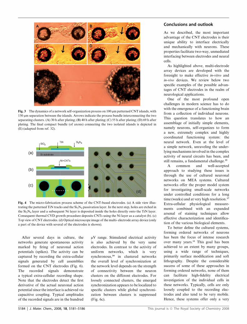
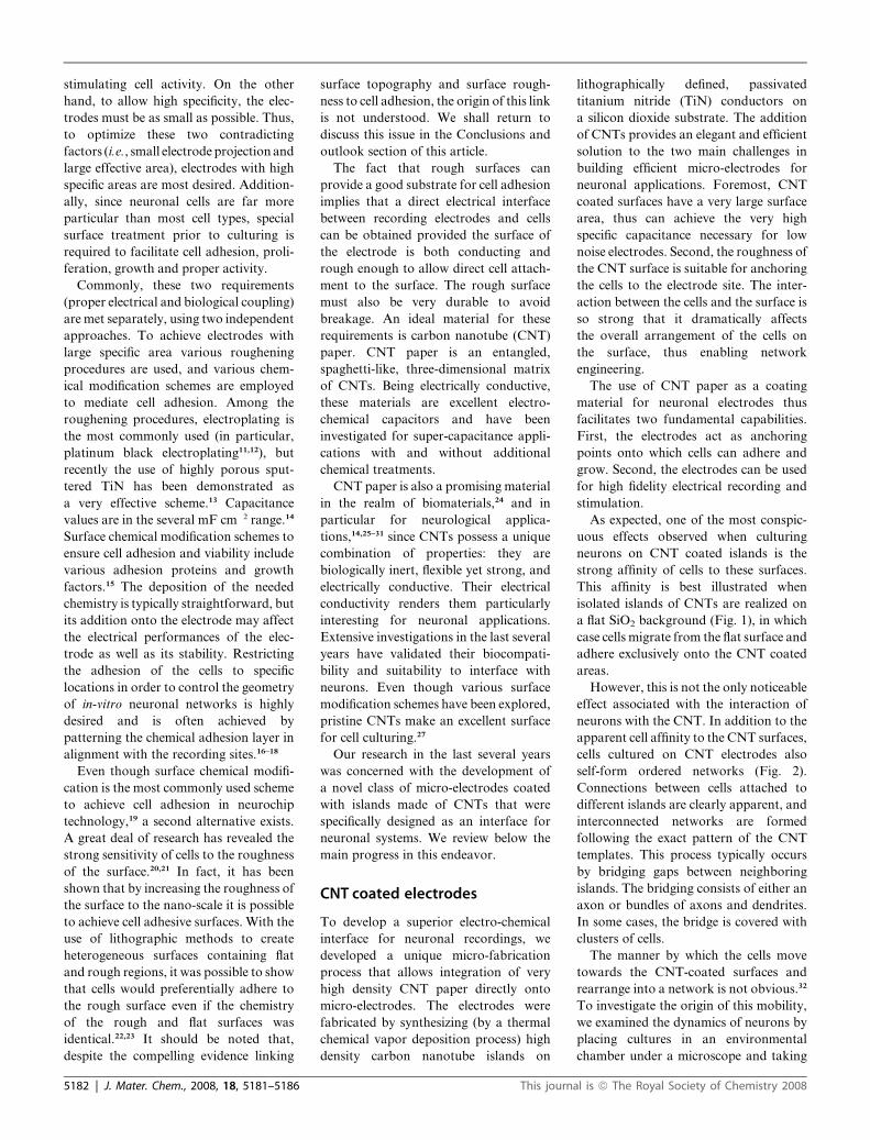
Fig. 3 The dynamics of a network self-organization process on 100 mm patterned CNT islands, with
150 mm separation between the islands. Arrows indicate the process bundle interconnecting the two
separating clusters. (A) 30 h after plating; (B) 40 h after plating; (C) 55 h after plating; (D) 69 h after
plating. The final compact bundle (of axons) connecting the two isolated islands is depicted in
(E) (adapted from ref. 32).
Fig. 4 The micro-fabrication process scheme of the CNT-based electrodes. (a) A side view illus-
trating the patterned TiN tracks and the Si3N4 passivation layer. In the next step, holes are etched in
the Si3N4 layer and a subsequent Ni layer is deposited inside the holes directly onto the TiN layer.
Consequent thermal CVD growth procedure deposits CNTs using the Ni layer as a catalyst (b). (c)
Top view of CNT electrodes. (d) Optical microscope image of the multi- electrode array device (only
a part of the device with several of the electrodes is shown).
After several days in culture, the
networks generate spontaneous activity
marked by firing of neuronal action
potentials (spikes). The activity can be
captured by recording the extra-cellular
signals generated by cell assemblies
formed on the CNT electrodes (Fig. 6).
The recorded signals demonstrate
a typical extra-cellular recording shape.
Note that the electrodes detect the first
derivative of the actual neuronal action
potential since the interface is achieved via
capacitive coupling. Typical amplitudes
of the recorded signals are in the hundred
5184 | J. Mater. Chem., 2008, 18, 5181–5186
mV range. Stimulated electrical activity
is also achieved by the very same
electrodes. In contrast to the activity of
uniform networks, which is very
synchronous,34 in clustered networks
the overall level of synchronization at
the network level depends on the strength
of connectivity between the neuron
clusters on the different electrodes. For
loosely connected clusters, the emerged
synchronization appears to be localized to
specific clusters while global synchroni-
zation between clusters is suppressed
(Fig. 6c).
This journ
Conclusions and outlook
As we described, the most important
advantage of the CNT electrodes is their
unique ability to interface electrically
and mechanically with neurons. These
properties facilitate two-way, unmediated
interfacing between electrodes and neural
cells.
As highlighted above, multi-electrode
array devices are developed with the
foresight to make effective in-vitro and
in-vivo devices. We review below two
specific examples of the possible advan-
tages of CNT electrodes in the realm of
neurological applications.
One of the most profound open
challenges in modern science has to do
with the emergence of a functioning brain
from a collection of individual neurons.
This question translates to how an
assemblage of initially simple elements,
namely neurons, self-organizes to form
a new, extremely complex and highly
coordinated functioning system: the
neural network. Even at the level of
a simple network, unraveling the under-
lying mechanisms involved in the complex
activity of neural circuits has been, and
still remains, a fundamental challenge.35
A common and well-accepted
approach to studying these issues is
through the use of cultured neuronal
networks on MEA systems. Cultured
networks offer the proper model system
for investigating small-scale networks
under controlled conditions for a long
time (weeks) and at very high resolution.17
Extra-cellular physiological measure-
ments combined with an expanded
arsenal of staining techniques allow
effective characterization and identifica-
tion of the various biological elements.
To better define the cultured systems,
forming ordered networks of neurons
has been the focus of intense research
over many years.11 This goal has been
achieved to an extent by many groups,
using a wide range of techniques,
primarily surface modification and soft
lithography. Despite the considerable
success of some of these approaches in
forming ordered networks, none of them
can facilitate high-fidelity electrical
investigation of the individual cells in
these networks. Typically, cells are only
loosely coupled to the recording elec-
trodes and also tend to be very mobile.
Hence, these systems offer only a very
al is ª The Royal Society of Chemistry 2008
Fig. 5 Optical microscope images of neurons on 80 mm CNT islands: (a) patterned interconnected
neuronal systems formed with pristine CNT islands. Closer inspections (by electron microscope
observations or staining) of the network in this case reveal that all the cells are attached to the CNT
islands. Note that cells attached to the electrodes are not visible in the optical image since the bases of
the electrodes are not transparent. For comparison, we show in (b) a random network formed on
a CNT island array coated with an adhesive protein layer. We can clearly see here cells that are
spread between the electrodes.
Fig. 6 Spontaneous electrical activity of
neuronal clusters on CNT electrodes. (a, b) A
voltage trace of spontaneous electrical activity
recorded from a CNT electrode. (c) A raster
plot of the spiking activity in several CNT
electrodes. Activity patterns are characterized
by synchronized bursting events (SBEs)—short
time windows (several hundreds of millisec-
onds) of rapid collective neuronal firing
followed by long intervals (tens of seconds) of
sporadic firing. The events of mutual synchro-
nization between the SBEs of different
electrodes are relatively rare in this example.
limited scope to investigate properties
related to coordinated activity of
neuronal circuits. For example, contem-
porary methods do not allow contin-
uous, multi-site, high resolution
investigation of signal propagation at the
single neuron level.
This journal is ª The Royal Society of Chemistry
The success of the CNT electrodes in
patterning and interfacing with neurons
suggests the unique possibility to carry
out investigations targeting basic
questions related to the activity of small
neuronal circuits. CNT electrodes facili-
tate the construction of the circuit as
well as provide the means to perform the
electrical recordings. Moreover, prelimi-
nary results demonstrate that the
CNT MEAs are also suitable for
interfacing with single cells at a very
high level of fidelity. By using cultures of
locust cells (neurons can be as large as
50 mm) we are now able to pattern
neuronal circuits consisting of ordered,
isolated single cells.
Moreover, since only very few neurons
occupy each electrode site, it is possible to
simultaneously monitor the activity of
these very small cell populations at
well known variable conditions such as
different degrees of connectivity to other
clusters, number of cells, number of glia
cells, etc. Such measurements could help
elucidate important aspects related to
cell–cell signaling, and in particular the
important influence of glia cell signaling
on neuronal activity and synchronization.
The high viability of the neuronal cells
on CNT surfaces, as is manifested in their
rapid development, also suggests their
potential in neuronal implant applica-
tions. In these devices, one of the major
challenges is the reactivity of the tissue
with the electrode surface. In retinal
implant devices, for example, one of the
major problems is the weak coupling
between the tissue and the electrodes,
which results in very poor stimulation
2008 J
specificity. The cells are simply too far
away from the electrode to allow stimu-
lation at high efficacy, in terms of both
charge injection and site specificity.
Preliminary tests we conducted have
validated the potential of this approach.
Mouse retinal whole mounts were placed
onto CNT MEAs, with ganglion cells (the
output cells of the retina) in direct contact
with the electrodes. Spontaneous bursts
of neural impulses as well as slow oscil-
latory activity were routinely recorded,
indicating the viability of these electrodes
for recording from intact neural tissue.
Successful stimulation tests were also
performed. We anticipate that the cell-
adhesive nature of our CNT electrodes, as
compared to standard microelectrodes
or even to vertically aligned, multi-walled
carbon nanotube microelectrodes, may
offer the important advantage of
promoting neuronal proliferation and
improving tissue–electrode interaction
without the need for additional adhesion
promoting coating.31
Even though the CNT electrodes
appear to be very effective, we believe that
their properties can be further enhanced
through surface modification. Special
chemical treatments can be applied to
improve the specificity of the electrodes
and to facilitate novel interfacing
schemes. It is also important to note
that the fabrication procedure currently
used to produce the CNT MEA employs a
relatively high temperature CVD proce-
dure, which restricts the range of
substrates used while also increasing the
fabrication cost relative to conventional
MEA. This drawback may be overcome
by developing alternative low-cost,
low-temperature procedures.
Our final comment is concerned with
the origin of the cell–CNT interaction.
Despite the great excitement in this field,
the underlying mechanism that governs
the interaction between cells and rough
surfaces in general, and with carbon
nanotubes in particular, is still elusive.
Our recent investigations into this issue
suggest a strong cellular sensitivity to
the surface roughness, which results
in process twining that may lead to cell
entanglement in the three dimensional
CNT matrix. Clearly, effective exploita-
tion of these surfaces in future bio-
medical devices strongly depends on
a better understanding of the biological
mechanisms involved.
. Mater. Chem., 2008, 18, 5181–5186 | 5185

Acknowledgements
This work was supported in part by an
ISF grant and by the Tauber Fund. The
authors thank Moshe David-Pur, Tamir
Gabay, Raya Sorkin, Alon Greenbaum,
Mark Shein, and Inna Brains who
contributed to and assisted in performing
the research described herein. YH thanks
Amir Ayali, Shlomo Yitzchaik, Evelyne
Sernagor, Chris Adams, and Danny
Baranes for very stimulating discussions.
References
1 J. Ji and K. D. Wise, An implantableCMOS circuit interface for multiplexedmicroelectrode recording arrays, IEEE J.Solid State Circuits, 1992, 27, 433–443.
2 Y. Jimbo and A. Kawana, Electricalstimulation and recording from culturedneurons using a planar electrode array,Bioelectrochem. Bioenerg., 1992, 29, 193.
3 P. Fromherz, C. O. Muller and R. Weis,Neuron transistor: electrical transferfunction measured by the patch-clamptechnique, Phys. Rev. Lett., 1993, 71,4079–4082.
4 M. P. Maher, J. Pine, J. Wright andY.-C. Tai, The neurochip: A newmultielectrode device for stimulatingand recording from cultured neurons,J. Neurosci. Methods, 1999, 87, 45–56.
5 S. Tatic-Lucic, Y.-C. Tai, J. A. Wright andJ. Pine, Silicon Cultured-Neuron ProstheticDevices for In Vivo and In Vitro Studies,Sens. Actuators, B: Chem., 1997, 43,105–109.
6 J. D. Weiland, W. Liu and M. S. Humayun,Retinal prosthesis, Annu. Rev. Biomed.Eng., 2005, 7, 361–401.
7 I. Baruchi and E. Ben-Jacob, TowardsNeuro-Memory-Chip: Imprinting multiplememories in cultured neural networks,Phys. Rev. E, 2007, 75, 050901.
8 E. Hulata, R. Segev, Y. Shapira,M. Benveniste and E. Ben-Jacob,Detection and sorting of neural spikesusing wavelet packets, Phys. Rev. Lett.,2000, 85, 4637–4640.
9 J. J. Pancrazio, S. A. Gray, Y. S. Subin,N. Kulagina, D. S. Cuttino,K. M. Shaffer, K. Eisemann, A. Curran,B. Zim, G. W. Gross andT. J. O’Shaughnessy, A portablemicroelectrode array recording systemincorporating cultured neuronal networksfor neurotoxin detection, Biosens.Bioelectron., 2003, 18(11), 1339–1347.
10 Y. Hanein, C. G. J. Schabmueller,G. Holman, P. Lucke, D. D. Denton andK. F. Bohringer, High-aspect ratio
5186 | J. Mater. Chem., 2008, 18, 5181–5186
submicrometer needles for intracellularapplications, J. Micromech. Microeng.,2003, 13, S91–S95.
11 C. D. James, A. J. H. Spence,N. M. Dowell-Mesfin, R. J. Hussain,K. L. Smith and H. G. Craighead,Extracellular recordings from patternedneuronal networks using planarmicroelectrode arrays, IEEE Trans.Biomed. Eng., 2004, 51, 1640–1645.
12 http://www.med64.com/products.html.13 M. Janders, U. Egert, M. Stelzle and
W. Nisch, Novel thin film titanium nitridemicro-electrodes with excellent chargetransfer capability for cell stimulation andsensing applications, Nano Lett., 1996, 1,245–247.
14 T. Gabay, M. Ben-David, I. Kalifa,R. Sorkin, Z. R. Abrams, E. Ben-Jacoband Y. Hanein, Electro-chemical andbiological properties of carbon nanotubebased multi-electrode arrays,Nanotechnology, 2007, 18, 035201.
15 M. Matsuzawa, S. Tokumitsu, W. Knolland H. Sasabe, Effects of organosilanemonolayer films on the geometricalguidance of CNS neurons, Langmuir,1998, 14, 5133–5138.
16 J. C. Chang, G. J. Brewer andB. C. Wheeler, Modulation of neuralnetwork activity by patterning, Biosens.Bioelectron., 2001, 16, 527.
17 R. Segev, M. Benveniste, E. Hulata,N. Cohen, A. Palevski, E. Kapon,Y. Shapira and E. Ben-Jacob, Long termbehavior of lithographically prepared invitro neuronal networks, Phys. Rev. Lett.,2002, 88, 118102.
18 A. Offenhausser, S. Bocker-Meffert,T. Decker, R. Helpenstein, P. Gasteier,J. Groll, M. Moller, A. Reska, S. Schafer,P. Schulte and A. Vogt-Eisele,Microcontact printing of proteins forneuronal cell guidance, Soft Matter, 2007,3, 290–298.
19 A. Folch and M. Toner, Microengineeringof cellular interactions, Annu. Rev.Biomed. Eng., 2000, 2, 227.
20 N. M. Dowell-Mesfin, M. A. Abdul-Karim,M. Turner, S. Schanz, H. G. Craighead,B. Roysam, J. N. Turner and W. Shain,Topographically modified surfaces affectorientation and growth of hippocampalneurons, J. Neural Eng., 2004, 1, 78–90.
21 S. K. Seidlits, J. Y. Lee and C. E. Schmidt,Nanostructured scaffolds for neuralapplications, Nanomedicine, 2008, 3,183–199.
22 Y. W. Fan and et al., Culture of neural cellson silicon wafers with nano-scale surfacetopography, J. Neurosci. Methods, 2002,120, 17–23.
23 C. C. Berry, G. Campbell, A. Spadiccino,M. Robertson and A. S. G. Curtis, Theinfluence of microscale topography on
This journ
fibroblast attachment and motility,Biomaterials, 2004, 25, 5781–5788.
24 E. Bekyarova, Y. Ni, E. B. Malarkey,V. Montana, J. L. McWilliams,R. C. Haddon and V. Parpura,Applications of Carbon Nanotubesin Biotechnology and Biomedicine,J. Biomed. Nanotechnol., 2005, 1, 3–17.
25 M. P. Mattson, R. C. Haddon andA. M. Rao, Molecular functionalization ofcarbon nanotubes and use as substratesfor neuronal growth, J. Mol. Neurosci.,2000, 14, 175–182.
26 H. Hu, Y. Ni, V. Montana, R. C. Haddonand V. Parpura, ChemicallyFunctionalized Carbon Nanotubes asSubstrates for Neuronal Growth, NanoLett., 2004, 4, 507–511.
27 T. Gabay, E. Jakobs, E. Ben-Jacob andY. Hanein, Carbon nanotube basedneuro-chip for engineering, recording andstimulation of cultured networks,Proceedings of the 13th InternationalConference on Solid-State Sensors,Actuators and Microsystems, IEEE,Piscataway, NJ, 2005, 2, 1226–1229.
28 T. Gabay, E. Jakobs, E. Ben-Jacob andY. Hanein, Engineered self-organizationof neural networks using carbon nanotubeclusters, Physica A, 2005, 350, 611–21.
29 V. Lovat, D. Pantarotto, L. Lagostena,B. Cacciari, M. Grandolfo, M. Righi,G. Spalluto, M. Prato and L. Ballerini,Carbon Nanotube Substrates BoostNeuronal Electrical Signaling, Nano Lett.,2005, 5–6, 1107–1110.
30 X. Zhang, S. Prasad, S. Niyogi, A. Morgan,M. Ozkan and C. S. Ozkan, Guided neuritegrowth on patterned carbon nanotubes,Sens. Actuators, B: Chem., 2005, 106, 843–850.
31 K. Wang, H. A. Fishman, H. Dai andJ. S. Harris, Neural Stimulation withCarbon Nanotube Microelectrode Array,Nano Lett., 2006, 6, 2043–2048.
32 R. Sorkin, T. Gabay, P. Blinder,D. Baranes, E. Ben-Jacob and Y. Hanein,compact self-wiring in cultured neuralnetworks, J. Neural Eng., 2006, 3, 95–101.
33 J. Li, A. Cassell, L. Delzeit, J. Han andM. Meyyappan, Novel three-dimensionalelectrodes: Electrochemical properties ofcarbon nanotube ensembles, J. Phys.Chem. B, 2002, 106, 9299–9305.
34 R. Segev, Y. Shapira, M. Benveniste andE. Ben-Jacob, Observation and modelingof synchronized bursting in two-dimensional neuronal networks, Phys.Rev. E, 2001, 64, 011920.
35 J. J. Hopfield, Neural Networks andPhysical Systems with Emergent CollectiveComputational Abilities, Proc. Natl. Acad.Sci. U. S. A., 1982, 79, 2554–2558.
al is ª The Royal Society of Chemistry 2008
Related Documents