Capacitance–voltage characteristics of metal–insulator–semiconductor structures based on graded-gap HgCdTe with various insulators A.V. Voitsekhovskii a, b, ⁎, S.N. Nesmelov b , S.M. Dzyadukh b a Department of Radiophysics, Tomsk State University, Lenin av., 36, 634050, Tomsk, Russia b Laboratory of Optical Electronics, Siberian Physical Technical Institute TSU, Novosobornaya sq., 1, 634050, Tomsk, Russia abstract article info Article history: Received 23 June 2011 Received in revised form 10 August 2012 Accepted 10 August 2012 Available online 19 August 2012 Keywords: Metal–insulator–semiconductor Mercury cadmium telluride Graded-gap layer Capacitance–voltage characteristics Interface Molecular-beam epitaxy Metal–insulator–semiconductor structures based on HgCdTe are grown by molecular-beam epitaxy. Near- surface graded-gap layers with a high CdTe content are inserted on both sides of the epitaxial HgCdTe film. The capacitance–voltage characteristics of these structures are studied experimentally. The main characteris- tics of these graded-gap HgCdTe structures are determined taking into account the effect of the non-uniform composition of the near-surface layers on the measured parameters. The capacitance–voltage characteristics of the graded-gap HgCdTe structures with various insulators are examined and the densities of surface states, densities of fixed and mobile charges are evaluated. The properties of the interface for CdTe grown in situ are found to be fairly good. We found that for structures based on HgCdTe–CdTe typical of very low density of mobile charges, the density of fixed charge does not exceed a 5.5 × 10 10 cm −2 . © 2012 Elsevier B.V. All rights reserved. 1. Introduction Narrow-band solid solution of Hg 1−x Cd x Te has been widely used for developing highly sensitive infrared detectors for the spectral ranges of atmospheric windows 3–5 and 8–12 μm for more than forty years [1]. Due to the necessity of passivation of the detectors' hybrid circuits and development of capabilities of monolithic circuit detectors, the properties of metal–insulator–semiconductor (MIS) structures based on bulk HgCdTe have been studied earlier in much detail [2–4]. The properties of the interfaces with HgCdTe of anodic oxide [5,5], its native sulfide [7], Al 2 O 3 [5], SiO 2 [5,8], ZnS [9–11], CdTe [12–15] and some other insulators are investigated. These results concern HgCdTe produced by bulk methods [5–11,13] or metalorganic chemical vapor deposition [12,14,15]. The development of molecular beam epitaxy (MBE) of HgCdTe has provided an additional means for optimizing the characteristics of in- frared photodetector arrays by controlling changes in the distribution of CdTe composition over the epitaxial film thickness [16–19]. The properties of MIS structures based on MBE HgCdTe with a stepped profile of composition [20] and a HgTe–CdTe superlattice in the active region [21] have been investigated. The band gap of HgCdTe depends on the composition of the CdTe, so the creation of near-surface graded-gap layers results to a potential barrier for minority carriers. Formation of compositionally graded surfaces (graded-gap layers) with a higher content of CdTe (higher value of x) compared to the bulk of the epitaxial film can improve the threshold characteristics of HgCdTe infrared detectors by reducing the influence of surface recombination on the photocarrier lifetime in the bulk of the epitaxial film [17–19]. Near-surface graded-gap layers with high composition can also be used for passivating detectors [22–24]. The characteristics of HgCdTe detectors largely depend on the properties (densities of fixed and mobile charges) of passivating insula- tor coatings and on their interfaces with the semiconductor (densities of surface states) [25,26], therefore, investigation into the characteris- tics of MIS structures based on heteroepitaxial MBE HgCdTe is an impor- tant task [27]. In the case of inhomogeneous distribution of the CdTe composition in the near-surface layer, no conventional methods devel- oped for homogeneous semiconductors can be used for determining the densities of surface states and densities of fixed and mobile charges. In [28], the effect on the capacitance–voltage characteristics of the pres- ence of graded-gap near-surface layer with linear variation of the band gap is considered theoretically, but no comparison of the calculation results with experiment is made. The electrical characteristics of MIS structures based on heteroepitaxial MBE HgCdTe layers with a near- surface graded gap are poorly understood [29–31]. In analyzing exper- imental capacitance–voltage characteristics of MIS structures based on graded-gap HgCdTe some authors either replace the real CdTe distribu- tion profile in the near-surface layer by a step profile [22] or do not consider the effect of the presence of graded-gap surface layer on the capacitance–voltage characteristics. The aim of this work is to develop methods to extract insulators and interface characteristics from capacitance–voltage measurements Thin Solid Films 522 (2012) 261–266 ⁎ Corresponding author. Tel.:+7 3822 412772; fax: +7 3822 422772. E-mail addresses: [email protected] (A.V. Voitsekhovskii), [email protected] (S.N. Nesmelov). 0040-6090/$ – see front matter © 2012 Elsevier B.V. All rights reserved. http://dx.doi.org/10.1016/j.tsf.2012.08.024 Contents lists available at SciVerse ScienceDirect Thin Solid Films journal homepage: www.elsevier.com/locate/tsf

Welcome message from author
This document is posted to help you gain knowledge. Please leave a comment to let me know what you think about it! Share it to your friends and learn new things together.
Transcript
Thin Solid Films 522 (2012) 261–266
Contents lists available at SciVerse ScienceDirect
Thin Solid Films
j ourna l homepage: www.e lsev ie r .com/ locate / ts f
Capacitance–voltage characteristics of metal–insulator–semiconductor structuresbased on graded-gap HgCdTe with various insulators
A.V. Voitsekhovskii a,b,⁎, S.N. Nesmelov b, S.M. Dzyadukh b
a Department of Radiophysics, Tomsk State University, Lenin av., 36, 634050, Tomsk, Russiab Laboratory of Optical Electronics, Siberian Physical Technical Institute TSU, Novosobornaya sq., 1, 634050, Tomsk, Russia
⁎ Corresponding author. Tel.:+7 3822 412772; fax: +E-mail addresses: [email protected] (A.V. Voitsekhov
(S.N. Nesmelov).
0040-6090/$ – see front matter © 2012 Elsevier B.V. Allhttp://dx.doi.org/10.1016/j.tsf.2012.08.024
a b s t r a c t
a r t i c l e i n f oArticle history:Received 23 June 2011Received in revised form 10 August 2012Accepted 10 August 2012Available online 19 August 2012
Keywords:Metal–insulator–semiconductorMercury cadmium tellurideGraded-gap layerCapacitance–voltage characteristicsInterfaceMolecular-beam epitaxy
Metal–insulator–semiconductor structures based on HgCdTe are grown by molecular-beam epitaxy. Near-surface graded-gap layers with a high CdTe content are inserted on both sides of the epitaxial HgCdTe film.The capacitance–voltage characteristics of these structures are studied experimentally. The main characteris-tics of these graded-gap HgCdTe structures are determined taking into account the effect of the non-uniformcomposition of the near-surface layers on the measured parameters. The capacitance–voltage characteristicsof the graded-gap HgCdTe structures with various insulators are examined and the densities of surface states,densities of fixed and mobile charges are evaluated. The properties of the interface for CdTe grown in situ arefound to be fairly good. We found that for structures based on HgCdTe–CdTe typical of very low density ofmobile charges, the density of fixed charge does not exceed a 5.5×1010 cm−2.
© 2012 Elsevier B.V. All rights reserved.
1. Introduction
Narrow-band solid solution ofHg1−xCdxTe has beenwidely used fordeveloping highly sensitive infrared detectors for the spectral rangesof atmospheric windows 3–5 and 8–12 μm for more than forty years[1]. Due to the necessity of passivation of the detectors' hybrid circuitsand development of capabilities of monolithic circuit detectors, theproperties of metal–insulator–semiconductor (MIS) structures basedon bulk HgCdTe have been studied earlier in much detail [2–4].The properties of the interfaces with HgCdTe of anodic oxide [5,5], itsnative sulfide [7], Al2O3 [5], SiO2 [5,8], ZnS [9–11], CdTe [12–15] andsome other insulators are investigated. These results concern HgCdTeproduced by bulk methods [5–11,13] or metalorganic chemical vapordeposition [12,14,15].
The development of molecular beam epitaxy (MBE) of HgCdTe hasprovided an additional means for optimizing the characteristics of in-frared photodetector arrays by controlling changes in the distributionof CdTe composition over the epitaxial film thickness [16–19]. Theproperties of MIS structures based on MBE HgCdTe with a steppedprofile of composition [20] and a HgTe–CdTe superlattice in the activeregion [21] have been investigated. The band gap of HgCdTe dependson the composition of the CdTe, so the creation of near-surfacegraded-gap layers results to a potential barrier for minority carriers.Formation of compositionally graded surfaces (graded-gap layers)
7 3822 422772.skii), [email protected]
rights reserved.
with a higher content of CdTe (higher value of x) compared to thebulk of the epitaxial film can improve the threshold characteristicsof HgCdTe infrared detectors by reducing the influence of surfacerecombination on the photocarrier lifetime in the bulk of the epitaxialfilm [17–19]. Near-surface graded-gap layers with high compositioncan also be used for passivating detectors [22–24].
The characteristics of HgCdTe detectors largely depend on theproperties (densities of fixed andmobile charges) of passivating insula-tor coatings and on their interfaces with the semiconductor (densitiesof surface states) [25,26], therefore, investigation into the characteris-tics ofMIS structures based on heteroepitaxialMBEHgCdTe is an impor-tant task [27]. In the case of inhomogeneous distribution of the CdTecomposition in the near-surface layer, no conventional methods devel-oped for homogeneous semiconductors can be used for determining thedensities of surface states and densities of fixed and mobile charges.In [28], the effect on the capacitance–voltage characteristics of the pres-ence of graded-gap near-surface layer with linear variation of the bandgap is considered theoretically, but no comparison of the calculationresults with experiment is made. The electrical characteristics of MISstructures based on heteroepitaxial MBE HgCdTe layers with a near-surface graded gap are poorly understood [29–31]. In analyzing exper-imental capacitance–voltage characteristics of MIS structures based ongraded-gap HgCdTe some authors either replace the real CdTe distribu-tion profile in the near-surface layer by a step profile [22] or do notconsider the effect of the presence of graded-gap surface layer on thecapacitance–voltage characteristics.
The aim of this work is to develop methods to extract insulatorsand interface characteristics from capacitance–voltage measurements
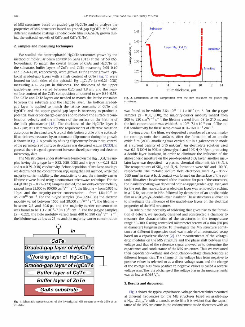
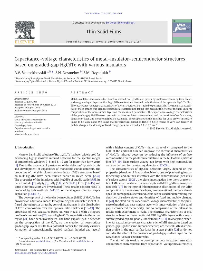
Fig. 2. Distribution of the composition over the film thickness for graded-gapstructures.
262 A.V. Voitsekhovskii et al. / Thin Solid Films 522 (2012) 261–266
of MIS structures based on graded-gap HgCdTe and to analyze theproperties of MIS structures based on graded-gap HgCdTe MBE withdifferent insulator coatings (anodic oxide film SiO2/Si3N4 grown dur-ing the epitaxial growth of CdTe and CdTe/ZnTe).
2. Samples and measuring techniques
We studied the heteroepitaxial HgCdTe structures grown by themethod of molecular beam epitaxy on GaAs (013) at the ISP SB RAS,Novosibirsk. To match the crystal lattices of GaAs and HgCdTe onthe substrate, buffer layers of ZnTe and CdTe measuring 0.05–0.10and 6.2–6.4 μm, respectively, were grown. During their growth, epi-taxial graded-gap layers with a high content of CdTe (Fig. 1) wereformed on both sides of the epitaxial Hg1−xCdxTe (x=0.21–0.38)measuring 4.1–12.4 μm in thickness. The thickness of the uppergraded-gap layers varied between 0.25 and 1.8 μm, and the near-surface content of the CdTe composition amounted to x=0.34–0.58.The CdTe and ZnTe layers are needed to match the lattice constantsbetween the substrate and the HgCdTe layer. The bottom graded-gap layer is applied to match the lattice constants of CdTe andHgCdTe, and the upper graded-gap layer is necessary to produce apotential barrier for charge-carriers and to reduce the surface recom-bination velocity and the influence of the surface on the lifetime ofthe bulk photocarrier [18]. The thickness of the HgCdTe layer is8–12 μm; it is determined by the requirements of effective radiationabsorption in the structure. A typical distribution profile of the epitaxial-film thicknessmeasured by an automatic ellipsometer during the growthis shown in Fig. 2. A possibility of using ellipsometry for an in situ controlof the parameters of this type structures was discussed, e.g., in [32,33]. Ingeneral, there is a good agreement between the ellipsometry and electronmicroscopy data.
TheMIS structures under studywere formedon theHg1−xCdxTe sam-ples having the p-type (x=0.22, 0.30, 0.38) and n-type (x=0.21–0.23and x=0.29–0.38) conductivity. Before deposition of insulator coatings,we determined the concentration n(p) using the Hall method, while themajority-carrier mobility μ, the conductivity σ, and the minority-carrierlifetime τ were found using a noncontact microwave technique. For then-HgCdTe (x=0.21–0.23) samples studied, the majority-carrier mobilityranged from 33,000 to 90,000 cm2V−1 s−1, the lifetime – from 0.035 to10 μs, and the majority-carrier concentration – from 1.8×10¹⁴ to4.9×1016 cm−3. For the n-type samples (x=0.29–0.38) the electronmobility varied between 1500 and 28,000 cm2V−1 s−1, the lifetime –
between 2.5 and 60.0 μs, and the majority-carrier concentrationwas found to be 1.3×10¹³–7.0×1014 cm−3. For the p-type samples(x=0.22), the hole mobility varied from 400 to 580 cm2 V−1 s−1,the lifetimewas as low as 75 ns, and themajority-carrier concentration
Fig. 1. Schematic representation of the investigated MIS structures with CdTe as aninsulator.
was found to be within 2.6×10¹⁵−1.1×1017 cm−3. For the p-typesamples (x=0.30, 0.38), the majority‐carrier mobility ranged from200 to 220 cm2V−1 s−1, the lifetime varied from 58 to 210 ns, andthe hole concentration was within 6.1×10¹⁵–7.1×1015 cm−3. The ini-tial conductivity for these samples was 0.01–160 Ω−1 cm−1.
Having grown the films, we deposited a number of various insula-tor coatings onto their surfaces. After the formation of an anodicoxide film (AOF), anodizing was carried out in a galvanostatic modeat a current density of 0.15 mA/cm2. An electrolyte solution usedwas 0.1 N KOH in 90% ethylene glycol and 10% H2O. Upon producinga double-layer insulator, in order to eliminate the influence of theatmospheric moisture on the pre-deposited SiO2 layer, another insu-lator layer was deposited — a plasma-chemical silicon nitride (Si3N4).The temperatures of SiO2 and Si3N4 formation were 90° and 100 °C,respectively. The metallic indium field electrodes were Ad=0.55×0.55 mm2 in size. A back contact was formed on the surface of the epi-taxialfilm after a local removal of the insulator. For part of the structures,the insulator coatingwas deposited onto an upper graded-gap layer, andfor the rest, the near-surface graded-gap layer was removed by etchingin a 1% Br2 solution in HBr, followed by deposition of an anodic oxidefilm or a SiO2/Si3N4 double-layer insulator. These structures allowed usto investigate the influence of the graded-gap layers on the electricalproperties of the MIS structures.
To rule out the necessity of soldering that gives rise to the forma-tion of defects, we specially designed and constructed a chamber tomeasure the characteristics of the structures in the temperaturerange 80–300 K using controlled micrometer screws of a thin (60 μmin diameter) tungsten probe. To investigate the MIS structure admit-tance at different frequencies used was made of an automated setupbased on a capacitive divider [2]. The measurements of the voltage-drop modulus on the MIS structure and the phase shift between thisvoltage and that of the reference signal allowed us to determine thecapacitance and conductance of the MIS structures. Thus we measuredtheir capacitance–voltage and conductance–voltage characteristics atdifferent frequencies. The change of the voltage bias from negative topositive values is referred to as a direct voltage scan, and the changeof the voltage bias from positive to negative values is called a reversevoltage scan. The rate of change of the voltage bias in themeasurementswas as low as 0.015 V/s.
3. Results and discussion
Fig. 3 shows the typical capacitance–voltage characteristics measuredat different frequencies for the MIS structures based on graded-gapn-Hg0.77Cd0.23Te with an anodic oxide film. It is evident that the capaci-tance of the MIS structure in the enhancement mode decreases with an
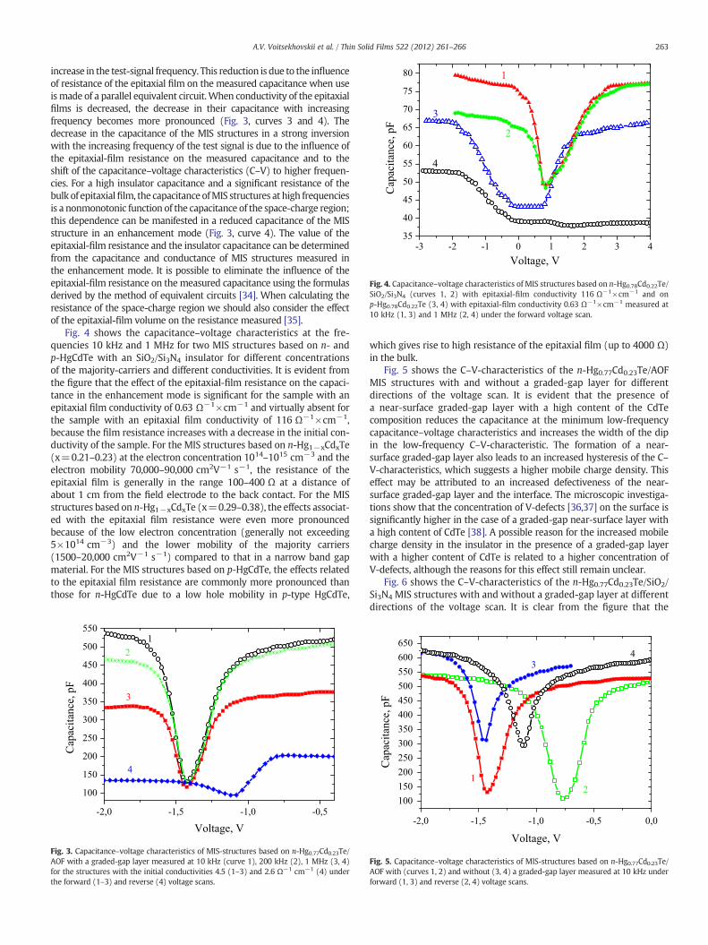
Fig. 4. Capacitance–voltage characteristics of MIS structures based on n-Hg0.78Cd0.22Te/SiO2/Si3N4 (curves 1, 2) with epitaxial-film conductivity 116 Ω−1×cm−1 and onp-Hg0.78Cd0.22Te (3, 4) with epitaxial-film conductivity 0.63 Ω−1×cm−1 measured at10 kHz (1, 3) and 1 MHz (2, 4) under the forward voltage scan.
263A.V. Voitsekhovskii et al. / Thin Solid Films 522 (2012) 261–266
increase in the test-signal frequency. This reduction is due to the influenceof resistance of the epitaxial film on the measured capacitance when useismade of a parallel equivalent circuit.When conductivity of the epitaxialfilms is decreased, the decrease in their capacitance with increasingfrequency becomes more pronounced (Fig. 3, curves 3 and 4). Thedecrease in the capacitance of the MIS structures in a strong inversionwith the increasing frequency of the test signal is due to the influence ofthe epitaxial-film resistance on the measured capacitance and to theshift of the capacitance–voltage characteristics (C–V) to higher frequen-cies. For a high insulator capacitance and a significant resistance of thebulk of epitaxialfilm, the capacitance ofMIS structures at high frequenciesis a nonmonotonic function of the capacitance of the space-charge region;this dependence can be manifested in a reduced capacitance of the MISstructure in an enhancement mode (Fig. 3, curve 4). The value of theepitaxial-film resistance and the insulator capacitance can be determinedfrom the capacitance and conductance of MIS structures measured inthe enhancement mode. It is possible to eliminate the influence of theepitaxial-film resistance on the measured capacitance using the formulasderived by the method of equivalent circuits [34]. When calculating theresistance of the space-charge region we should also consider the effectof the epitaxial-film volume on the resistance measured [35].
Fig. 4 shows the capacitance–voltage characteristics at the fre-quencies 10 kHz and 1 MHz for two MIS structures based on n- andp-HgCdTe with an SiO2/Si3N4 insulator for different concentrationsof the majority-carriers and different conductivities. It is evident fromthe figure that the effect of the epitaxial-film resistance on the capaci-tance in the enhancement mode is significant for the sample with anepitaxial film conductivity of 0.63 Ω−1×cm−1 and virtually absent forthe sample with an epitaxial film conductivity of 116 Ω−1×cm−1,because the film resistance increases with a decrease in the initial con-ductivity of the sample. For the MIS structures based on n-Hg1−xCdxTe(x=0.21–0.23) at the electron concentration 1014–1015 cm−3 and theelectron mobility 70,000–90,000 cm2V−1 s−1, the resistance of theepitaxial film is generally in the range 100–400 Ω at a distance ofabout 1 cm from the field electrode to the back contact. For the MISstructures based on n-Hg1−xCdxTe (x=0.29–0.38), the effects associat-ed with the epitaxial film resistance were even more pronouncedbecause of the low electron concentration (generally not exceeding5×1014 cm−3) and the lower mobility of the majority carriers(1500–20,000 cm2V−1 s−1) compared to that in a narrow band gapmaterial. For the MIS structures based on p-HgCdTe, the effects relatedto the epitaxial film resistance are commonly more pronounced thanthose for n-HgCdTe due to a low hole mobility in p-type HgCdTe,
Fig. 3. Capacitance–voltage characteristics of MIS-structures based on n-Hg0.77Cd0.23Te/AOF with a graded-gap layer measured at 10 kHz (curve 1), 200 kHz (2), 1 MHz (3, 4)for the structures with the initial conductivities 4.5 (1–3) and 2.6 Ω−1 cm−1 (4) underthe forward (1–3) and reverse (4) voltage scans.
which gives rise to high resistance of the epitaxial film (up to 4000 Ω)in the bulk.
Fig. 5 shows the C–V-characteristics of the n-Hg0.77Cd0.23Te/AOFMIS structures with and without a graded-gap layer for differentdirections of the voltage scan. It is evident that the presence ofa near-surface graded-gap layer with a high content of the CdTecomposition reduces the capacitance at the minimum low-frequencycapacitance–voltage characteristics and increases the width of the dipin the low-frequency C–V-characteristic. The formation of a near-surface graded-gap layer also leads to an increased hysteresis of the C–V-characteristics, which suggests a higher mobile charge density. Thiseffect may be attributed to an increased defectiveness of the near-surface graded-gap layer and the interface. The microscopic investiga-tions show that the concentration of V-defects [36,37] on the surface issignificantly higher in the case of a graded-gap near-surface layer witha high content of CdTe [38]. A possible reason for the increased mobilecharge density in the insulator in the presence of a graded-gap layerwith a higher content of CdTe is related to a higher concentration ofV-defects, although the reasons for this effect still remain unclear.
Fig. 6 shows the C–V-characteristics of the n-Hg0.77Cd0.23Te/SiO2/Si3N4 MIS structures with and without a graded-gap layer at differentdirections of the voltage scan. It is clear from the figure that the
Fig. 5. Capacitance–voltage characteristics of MIS-structures based on n-Hg0.77Cd0.23Te/AOF with (curves 1, 2) and without (3, 4) a graded-gap layer measured at 10 kHz underforward (1, 3) and reverse (2, 4) voltage scans.
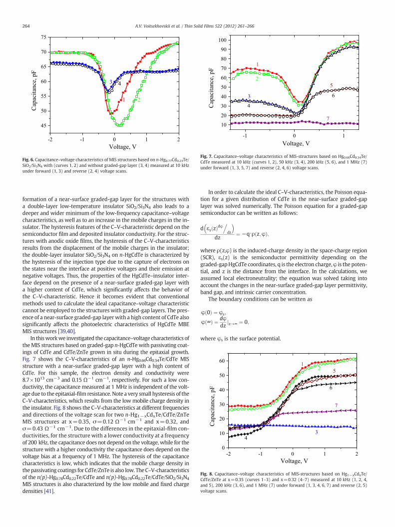
Fig. 6. Capacitance–voltage characteristics of MIS structures based on n-Hg0.77Cd0.23Te/SiO2/Si3N4 with (curves 1, 2) and without graded-gap layer (3, 4) measured at 10 kHzunder forward (1, 3) and reverse (2, 4) voltage scans.
Fig. 7. Capacitance–voltage characteristics of MIS-structures based on Hg0.66Cd0.34Te/CdTe measured at 10 kHz (curves 1, 2), 50 kHz (3, 4), 200 kHz (5, 6), and 1 MHz (7)under forward (1, 3, 5, 7) and reverse (2, 4, 6) voltage scans.
Fig. 8. Capacitance–voltage characteristics of MIS-structures based on Hg1−xCdxTe/CdTe/ZnTe at x=0.35 (curves 1–3) and x=0.32 (4–7) measured at 10 kHz (1, 2, 4,and 5), 200 kHz (3, 6), and 1 MHz (7) under forward (1, 3, 4, 6, 7) and reverse (2, 5)voltage scans.
264 A.V. Voitsekhovskii et al. / Thin Solid Films 522 (2012) 261–266
formation of a near-surface graded-gap layer for the structures witha double-layer low-temperature insulator SiO2/Si3N4 also leads to adeeper and wider minimum of the low-frequency capacitance–voltagecharacteristics, as well as to an increase in the mobile charges in the in-sulator. The hysteresis features of the C–V-characteristic depend on thesemiconductor film and deposited insulator conductivity. For the struc-tures with anodic oxide films, the hysteresis of the C–V-characteristicsresults from the displacement of the mobile charges in the insulator;the double-layer insulator SiO2/Si3N4 on n-HgCdTe is characterized bythe hysteresis of the injection type due to the capture of electrons onthe states near the interface at positive voltages and their emission atnegative voltages. Thus, the properties of the HgCdTe–insulator inter-face depend on the presence of a near-surface graded-gap layer witha higher content of CdTe, which significantly affects the behavior ofthe C–V-characteristic. Hence it becomes evident that conventionalmethods used to calculate the ideal capacitance–voltage characteristiccannot be employed to the structures with graded-gap layers. The pres-ence of a near-surface graded-gap layerwith a high content of CdTe alsosignificantly affects the photoelectric characteristics of HgCdTe MBEMIS structures [39,40].
In thisworkwe investigated the capacitance–voltage characteristics oftheMIS structures based on graded-gap n-HgCdTe with passivating coat-ings of CdTe and CdTe/ZnTe grown in situ during the epitaxial growth.Fig. 7 shows the C–V-characteristics of an n-Hg0.66Cd0.34Te/CdTe MISstructure with a near-surface graded-gap layer with a high content ofCdTe. For this sample, the electron density and conductivity were8.7×1013 cm−3 and 0.15 Ω−1 cm−1, respectively. For such a low con-ductivity, the capacitance measured at 1 MHz is independent of the volt-age due to the epitaxial-film resistance. Note a very small hysteresis of theC–V-characteristics, which results from the low mobile charge density inthe insulator. Fig. 8 shows the C–V-characteristics at different frequenciesand directions of the voltage scan for two n-Hg1−xCdxTe/CdTe/ZnTeMIS structures at x=0.35, σ=0.12 Ω−1 cm−1 and x=0.32, andσ=0.43 Ω−1 cm−1. Due to the differences in the epitaxial-film con-ductivities, for the structure with a lower conductivity at a frequencyof 200 kHz, the capacitance does not depend on the voltage, while for thestructure with a higher conductivity the capacitance does depend on thevoltage bias at a frequency of 1 MHz. The hysteresis of the capacitancecharacteristics is low, which indicates that the mobile charge density inthepassivating coatings for CdTe/ZnTe is also low. TheC–V-characteristicsof the n(p)-Hg0.78Cd0.22Te/CdTe and n(p)-Hg0.78Cd0.22Te/CdTe/SiO2/Si3N4
MIS structures is also characterized by the low mobile and fixed chargedensities [41].
In order to calculate the ideal C–V-characteristics, the Poisson equa-tion for a given distribution of CdTe in the near-surface graded-gaplayer was solved numerically. The Poisson equation for a graded-gapsemiconductor can be written as follows:
d εs zð Þdφ.
dz
� �dz
¼ −q⋅ρ z;φð Þ;
where ρ(z,φ) is the induced-charge density in the space-charge region(SCR), εs(z) is the semiconductor permittivity depending on thegraded-gapHgCdTe coordinates, q is the electron charge,φ is the poten-tial, and z is the distance from the interface. In the calculations, weassumed local electroneutrality; the equation was solved taking intoaccount the changes in the near-surface graded-gap layer permittivity,band gap, and intrinsic carrier concentration.
The boundary conditions can be written as
φ 0ð Þ ¼ φs;
φ ∞ð Þ ¼ dφdz z→∞ ¼ 0;j
where φs is the surface potential.
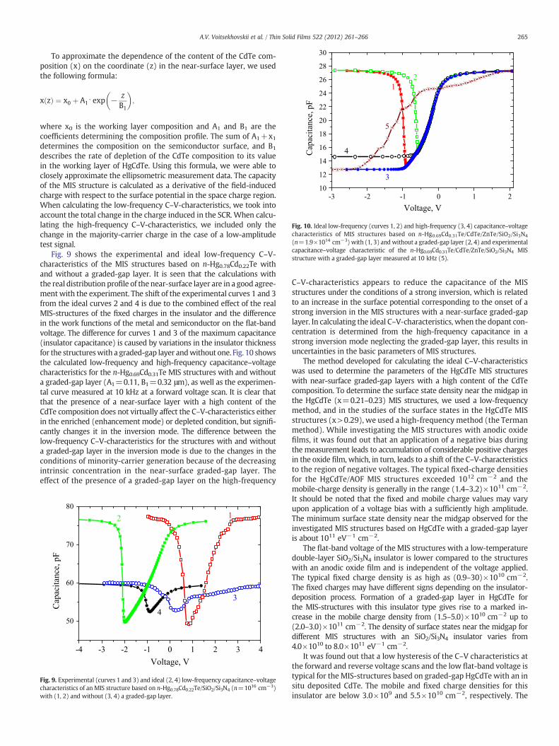
Fig. 10. Ideal low-frequency (curves 1, 2) and high-frequency (3, 4) capacitance–voltagecharacteristics of MIS structures based on n-Hg0.69Cd0.31Te/CdTe/ZnTe/SiO2/Si3N4
(n=1.9×1014 cm−3) with (1, 3) and without a graded-gap layer (2, 4) and experimentalcapacitance–voltage characteristic of the n-Hg0.69Cd0.31Te/CdTe/ZnTe/SiO2/Si3N4 MISstructure with a graded-gap layer measured at 10 kHz (5).
265A.V. Voitsekhovskii et al. / Thin Solid Films 522 (2012) 261–266
To approximate the dependence of the content of the CdTe com-position (x) on the coordinate (z) in the near-surface layer, we usedthe following formula:
x zð Þ ¼ x0 þ A1⋅ exp − zB1
� �;
where x0 is the working layer composition and A1 and B1 are thecoefficients determining the composition profile. The sum of A1+x1determines the composition on the semiconductor surface, and B1
describes the rate of depletion of the CdTe composition to its valuein the working layer of HgCdTe. Using this formula, we were able toclosely approximate the ellipsometric measurement data. The capacityof the MIS structure is calculated as a derivative of the field-inducedcharge with respect to the surface potential in the space charge region.When calculating the low-frequency C–V-characteristics, we took intoaccount the total change in the charge induced in the SCR. When calcu-lating the high-frequency C–V-characteristics, we included only thechange in the majority-carrier charge in the case of a low-amplitudetest signal.
Fig. 9 shows the experimental and ideal low-frequency C–V-characteristics of the MIS structures based on n-Hg0.78Cd0.22Te withand without a graded-gap layer. It is seen that the calculations withthe real distribution profile of the near-surface layer are in a good agree-ment with the experiment. The shift of the experimental curves 1 and 3from the ideal curves 2 and 4 is due to the combined effect of the realMIS-structures of the fixed charges in the insulator and the differencein the work functions of the metal and semiconductor on the flat-bandvoltage. The difference for curves 1 and 3 of the maximum capacitance(insulator capacitance) is caused by variations in the insulator thicknessfor the structureswith a graded-gap layer andwithout one. Fig. 10 showsthe calculated low-frequency and high-frequency capacitance–voltagecharacteristics for the n-Hg0.69Cd0.31Te MIS structures with and withouta graded-gap layer (A1=0.11, B1=0.32 μm), as well as the experimen-tal curve measured at 10 kHz at a forward voltage scan. It is clear thatthat the presence of a near-surface layer with a high content of theCdTe composition does not virtually affect the C–V-characteristics eitherin the enriched (enhancement mode) or depleted condition, but signifi-cantly changes it in the inversion mode. The difference between thelow-frequency C–V-characteristics for the structures with and withouta graded-gap layer in the inversion mode is due to the changes in theconditions of minority-carrier generation because of the decreasingintrinsic concentration in the near-surface graded-gap layer. Theeffect of the presence of a graded-gap layer on the high-frequency
Fig. 9. Experimental (curves 1 and 3) and ideal (2, 4) low-frequency capacitance–voltagecharacteristics of an MIS structure based on n-Hg0.78Cd0.22Te/SiO2/Si3N4 (n=1016 cm−3)with (1, 2) and without (3, 4) a graded-gap layer.
C–V-characteristics appears to reduce the capacitance of the MISstructures under the conditions of a strong inversion, which is relatedto an increase in the surface potential corresponding to the onset of astrong inversion in the MIS structures with a near-surface graded-gaplayer. In calculating the ideal C–V-characteristics, when the dopant con-centration is determined from the high-frequency capacitance in astrong inversion mode neglecting the graded-gap layer, this results inuncertainties in the basic parameters of MIS structures.
The method developed for calculating the ideal C–V-characteristicswas used to determine the parameters of the HgCdTe MIS structureswith near-surface graded-gap layers with a high content of the CdTecomposition. To determine the surface state density near the midgap inthe HgCdTe (x=0.21–0.23) MIS structures, we used a low-frequencymethod, and in the studies of the surface states in the HgCdTe MISstructures (x>0.29), we used a high-frequency method (the Termanmethod). While investigating the MIS structures with anodic oxidefilms, it was found out that an application of a negative bias duringthe measurement leads to accumulation of considerable positive chargesin the oxide film, which, in turn, leads to a shift of the C–V-characteristicsto the region of negative voltages. The typical fixed-charge densitiesfor the HgCdTe/AOF MIS structures exceeded 1012 cm−2 and themobile-charge density is generally in the range (1.4–3.2)×1011 cm−2.It should be noted that the fixed and mobile charge values may varyupon application of a voltage bias with a sufficiently high amplitude.The minimum surface state density near the midgap observed for theinvestigated MIS structures based on HgCdTe with a graded-gap layeris about 1011 eV−1 cm−2.
The flat-band voltage of the MIS structures with a low-temperaturedouble-layer SiO2/Si3N4 insulator is lower compared to the structureswith an anodic oxide film and is independent of the voltage applied.The typical fixed charge density is as high as (0.9–30)×1010 cm−2.The fixed charges may have different signs depending on the insulator-deposition process. Formation of a graded-gap layer in HgCdTe forthe MIS-structures with this insulator type gives rise to a marked in-crease in the mobile charge density from (1.5–5.0)×1010 cm−2 up to(2.0–3.0)×1011 cm−2. The density of surface states near the midgap fordifferent MIS structures with an SiO2/Si3N4 insulator varies from4.0×1010 to 8.0×10¹¹ eV−1 cm−2.
It was found out that a low hysteresis of the C–V characteristics atthe forward and reverse voltage scans and the low flat-band voltage istypical for the MIS-structures based on graded-gap HgCdTe with an insitu deposited CdTe. The mobile and fixed charge densities for thisinsulator are below 3.0×10⁹ and 5.5×1010 cm−2, respectively. The
266 A.V. Voitsekhovskii et al. / Thin Solid Films 522 (2012) 261–266
density of surface states near the midgap for CdTe is generally nohigher than 2.7×10¹¹ eV−1 cm−2.
Formation of an additional layer ZnTe on top of CdTe frequentlyleads to an increase in the average density of surface states in theHgCdTe (x=0.32–0.35)–CdTe (up to 5.0×10¹¹ eV−1 cm−2) system.When forming an additional ZnTe layer, we observed a moderateincrease in mobile charges in the insulator (up to 6.8×109 cm−2),while the fixed charge density was found to decrease (down to5.5×108–2.0×1010 cm−2).
We observed that for the MIS-structures with a complex protec-tive insulator CdTe/ZnTe/SiO2/Si3N4 a positive fixed charge in theinsulator and an increase in the density of surface states are common.
4. Summary
The capacitance–voltage characteristics of the MIS-structuresbased on hetero-epitaxial graded-gap HgCdTe grown by molecularbeam epitaxy with different insulators were investigated (AOF,SiO2/Si3N4, CdTe, CdTe/ZnTe, CdTe/ZnTe/SiO2/Si3N4). It was shownthat the resistance of the epitaxial film significantly affects themeasuredelectrical characteristics of MIS structures based on HgCdTeMBE at highfrequencies of the test signal (for example, higher than 200 kHz for theMIS structures based on n-Hg1−xCdxTe at x=0.21–0.23). It was foundthat the formation of a near-surface graded-gap layer with a high CdTecontent in the epitaxial HgCdTe film leads to changes in the low- andhigh-frequency capacitance–voltage characteristics in the inversionmode. The formation of the near-surface graded-gap layer also leads toan increase in the density of mobile charges for the MIS-structureswith AOF and SiO2/Si3N4 insulators. A method for calculating the idealcapacitance–voltage characteristics of the MIS-structures based onMBEHgCdTewith near-surface graded-gap layers with a high CdTe con-tent has been developed. Using the technique theproperties of the inter-faces between graded-gapHgCdTe and different insulator coatingswereinvestigated. A reasonably high positive fixed charge (higher than1.4×1011 cm−2) is typical for the anodic oxide film, which allows oneto use it for passivating photoconductors based on n-HgCdTe alone.The results are in good agreementwith the literature data (for example,in [6], the density of a fixed charge for the native oxide on HgCdTe bulkgrown by the Bridgman–Stockberger method was 1–1.5×1011 cm−2).Under passivation by a low-temperature double-layer SiO2/Si3N4
insulator there appears a significant mobile charge (higher than2×1011 cm−2), which can lead to instability of the devices used.This density of mobile charges significantly exceeds that of structureswithout a graded-gap layer. The density of mobile charges for SiO2 onHgCdTe without a graded-gap layer at x≈0.2 is (2–3)×1010 cm−2
[6]. Relatively low densities of fixed (lower than 5.5×1010 cm−2) andthe mobile charges (lower than 7×109 cm−2) are typical of insulatorcoatings of CdTe and CdTe/ZnTe grown in situ during the epitaxialgrowth. The properties of metalorganic chemical vapor depositiongrowth of CdTe on bulk HgCdTe have been investigated and the fixedcharge density varied between 8.8×1010 cm−2 and 6.5×1011 cm−2
depending on the preparation conditions (growth temperature,annealing) [14]. The hysteresis of the capacitance–voltage characteris-tics for some samples was low [14], however, for some structures thedensity ofmobile charge amounted to 2.5×1010 cm−2 [15]. In addition,CdTe has a high radiation resistance and the possibility of improving theproperties of the interface of CdTe with graded-gap HgCdTe throughoptimization of epitaxial growth has not been fully exhausted. Deposi-tion of additional SiO2/Si3N4 sublayers on top of CdTe/ZnTe leads tosome increase in the positive fixed charge and to some increase in thedensity of surface states. Thus, deposition of passivating CdTe andCdTe/ZnTe grown in situ on top of MBE HgCdTe with a near-surfacegraded-gap layer with a high CdTe content leads to the formation of
high-quality interface with low density of fixed and virtual absence ofmobile charges.
Acknowledgments
This work was supported by the Federal Target Program “Researchand Scientific-Pedagogical Stuff of Innovative Russia” (2009–2012),Project GK 02.740.11.0562, Reg. No. 15157 and by the Grant of theRussian President for Support of the Leading Scientific SchoolsNSH-512.2012.2.
References
[1] A. Rogalsky, Infrared Detectors, 2nd. ed. CRC Press, Taylor & Francis Group, NewYork, 2011. 876 p.
[2] M.A. Kinch, Semicond. Semimetals 18 (1981) 313.[3] A.V. Voitsekhovskii, V.N. Davydov, in: Photoelectric MIS Structures Based on
Narrow-Band Semiconductors, Radio Svyaz, Tomsk, 1990, p. 327.[4] C.-H. Lin, C.W. Liu, Sensors 10 (2010) 8797.[5] N.T.B. Ngoc, N.V. Nha, Thin Solid Films 334 (1998) 40.[6] V. Damnjanovic, J.M. Elazar, in: N. Stojadinovic, S. Dimitrijev, H. Iwai, J. Liou, S.
Selberherr (Eds.), Microelectronics 2010 (MIEL 2010), Proceedings of the 27thInternational Conference on Microelectronics, NIS, Serbia, May 16–19, 2010, p. 131.
[7] Y. Nemirovsky, L. Burstein, I. Kidron, J. Appl. Phys. 58 (1986) 366.[8] G.H. Tsau, A. Sher, M. Madou, J.A. Wilson, V.A. Cotton, C.E. Jones, J. Appl. Phys. 59
(1986) 1238.[9] M.J. Yang, C.H. Yang, M.A. Kinch, J.D. Beck, J. Appl. Phys. 54 (1989) 265.
[10] R.K. Bhan, V. Srivastava, R.S. Saxena, L. Sareen, R. Pal, R.K. Sharma, Infrared Phys.Technol. 53 (2010) 404.
[11] P.V. Biryulin, S.A. Dudko, S.A. Konovalov, Yu.A. Pelevin, V.I. Turinov, Semiconductors37 (2003) 1383.
[12] G. Bahir, V. Ariel, V. Garber, D. Rosenfeld, A. Sher, Appl. Phys. Lett. 65 (1994) 2725.[13] V. Kumar, R. Pal, P.K. Chaudhury, B.L. Sharma, V. Gopal, J. Electron. Mater. 34
(2005) 1225.[14] Y. Nemirovsky, N. Amir, D. Goren, G. Asa, J. Electron. Mater. 24 (1995) 1161.[15] Y. Nemirovsky, N. Amir, L. Djaloshinski, J. Electron. Mater. 24 (1995) 647.[16] M.A. Kinch, J. Electron. Mater. 39 (2010) 1043.[17] A.V. Voitsekhovskii, Yu.A. Denisov, A.P. Kokhanenko, V.S. Varavin, S.A. Dvoretskii,
V.T. Liberman, N.N. Mikhailov, Yu.G. Sidorov, Semiconductors 31 (1997) 655.[18] V.N. Ovsyk, G.L. Kuryshev, Y.G. Sidorov, in: IR-Matrix Photodetectors, Nauka,
Novosibirsk, 2001, p. 376.[19] V.S. Varavin, V.V. Vasiliev, S.A. Dvoretsky, N.N. Mikhailov, V.N. Ovsyuk, Yu.G.
Sidorov, A.O. Suslyakov, M.V. Yakushev, Opto-Electron. Rev. 11 (2003) 99.[20] M.W. Goodwin, M.A. Kinch, R.J. Koestner, J. Vac. Sci. Technol. A8 (2) (1990) 1226.[21] M.W. Goodwin, M.A. Kinch, R.J. Koestner, J. Vac. Sci. Technol. A6 (4) (1988) 2685.[22] S.Y. An, J.S. Kim, D.W. Seo, S.H. Suh, J. Electron. Mater. 31 (2002) 683.[23] R. Pal, A. Malik, V. Srivastav, B.L. Sharma, V. Dhar, B. Sreedhar, H.P. Vyas, J.
Electron. Mater. 35 (2006) 1793.[24] R. Pal, A. Malik, V. Srivastav, B.L. Sharma, V.R. Balakrishnan, V. Dhar, H.P. Vyas,
IEEE Trans. Electron Devices 53 (2006) 2727.[25] O.P. Agnihorti, C.A. Musca, L. Faraone, Semicond. Sci. Technol. 13 (1998) 839.[26] P. Capper, J. Garland, S. Kasap, A. Willoughby, in: JohnWiley & Sons Ltd, Chichester,
United Kingdom, 2011, p. 563.[27] I.S. Virt, I.V. Kurilo, I.A. Rudyi, F.F. Sizov, N.N. Mikhailov, R.N. Smirnov, Semicon-
ductors 42 (2008) 772.[28] E.V. Buzaneva, in: Microstructure of Integral Electronics, Radio and Svyaz,
Moscow, 1990, p. 304.[29] V.N. Ovsyuk, A.V. Yartsev, Proc. SPIE 6636 (2007) 663617.[30] V.V. Vasil'ev, Yu.P. Mashukov, Semiconductors 41 (2007) 37.[31] A.A. Guzev, V.S. Varavin, S.A. Dvoretsky, A.P. Kovchavtsev, G.L. Kuryshev, I.I. Lee,
Z.V. Panova, Yu.G. Sidorov, M.V. Yakushev, Appl. Phys. 2 (2009) 92 (in Russian).[32] V.A. Shvets, Opt. Spectrosc. 107 (2009) 780.[33] V.A. Shvets, S.V. Rykhlitski, E.V. Spesivtsev, N.A. Aulchenko, N.N. Mikhailov, S.A.
Dvoretsky, Yu.G. Sidorov, R.N. Smirnov, Thin Solid Films 455–456 (2004) 688.[34] A.V. Voitsekhovskii, S.N. Nesmelov, S.M. Dzyadukh, Russ. Phys. J. 48 (2005) 584.[35] A.V. Voitsekhovkii, S.N. Nesmelov, S.M. Dzyadukh, Russ. Phys. J. 52 (2009) 1003.[36] I.V. Sabinina, A.K. Gutakovsky, Yu.G. Sidorov, A.V. Latushev, J. Cryst. Growth 274
(2005) 339.[37] M.V. Yakushev, D.V. Brunev, V.S. Varavin, V.V. Vasilyev, S.A. Dvoretskii, I.V.
Marchishin, A.V. Predein, I.V. Sabinina, Yu.G. Sidorov, A.V. Sorochkin, Semicon-ductors 45 (2011) 385.
[38] A.S. Kashuba, A.V. Zabolotsky, E.V. Korostylev, A.A. Kuzin, E.V. Permikina, V.V.Arbenina, Vestnik MITHT 5 (2010) 19 (in Russian).
[39] A.V. Voitsekhovskii, S.N. Nesmelov, S.M. Dzyadukh, V.S. Varavin, S.A. Dvoretskii,N.N. Mikhailov, Yu.G. Sidorov, V.V. Vasil'ev, Semiconductors 42 (2008) 1327.
[40] A.V. Voitsekhovskii, S.N. Nesmelov, S.M. Dzyadukh, V.S. Varavin, S.A. Dvoretskii,N.N. Mikhailov, Yu.G. Sidorov, M.V. Yakushev, Opto-Electron. Rev. 18 (2010) 259.
[41] A.V. Voitsekhovskii, S.N. Nesmelov, S.M. Dzyadukh, V.S. Varavin, S.A. Dvoretskii,N.N. Mikhailov, Yu.G. Sidorov, M.V. Yakushev, Opto-Electron. Rev. 18 (2010) 263.
Related Documents


![[ Registration ] Silicon & Diamond photonicsFemto-ST SCIENCES & TECHNOLOGIES Besancon, France Lunch break 12:45 hrs [ 09.03.2016 ] Diamond Nanophotonics centers in diamond 09:30 hrs](https://static.cupdf.com/doc/110x72/60159bc2f38a064e2a3c303a/-registration-silicon-diamond-photonics-femto-st-sciences-technologies.jpg)


