CANON INDUSTRIAL PRODUCTS ENABLING A WORLD OF INNOVATIONS

Welcome message from author
This document is posted to help you gain knowledge. Please leave a comment to let me know what you think about it! Share it to your friends and learn new things together.
Transcript

C A N O N I N D U S T R I A L P R O D U C T S
ENABLING A WORLD OF INNOVATIONS
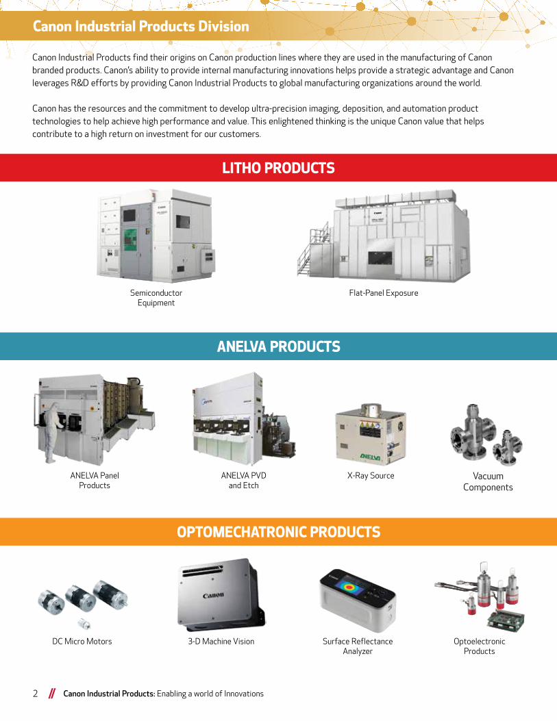
Canon Industrial Products Division
2 Canon Industrial Products: Enabling a world of Innovations
LITHO PRODUCTS
ANELVA PRODUCTS
OPTOMECHATRONIC PRODUCTS
Canon Industrial Products find their origins on Canon production lines where they are used in the manufacturing of Canon branded products. Canon’s ability to provide internal manufacturing innovations helps provide a strategic advantage and Canon leverages R&D efforts by providing Canon Industrial Products to global manufacturing organizations around the world.
Canon has the resources and the commitment to develop ultra-precision imaging, deposition, and automation product technologies to help achieve high performance and value. This enlightened thinking is the unique Canon value that helps contribute to a high return on investment for our customers.
Semiconductor Equipment
Flat-Panel Exposure
ANELVA PanelProducts
X-Ray Source
DC Micro Motors Surface ReflectanceAnalyzer
ANELVA PVD and Etch
VacuumComponents
OptoelectronicProducts
3-D Machine Vision
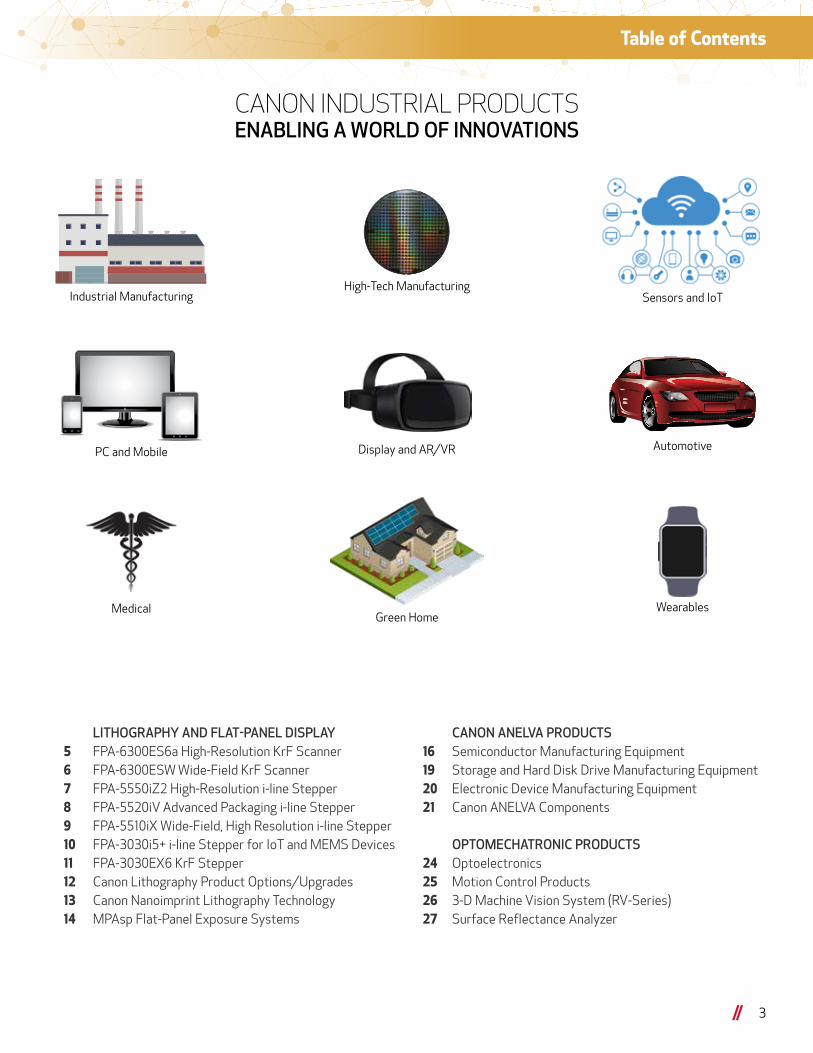
Table of Contents
3
LITHOGRAPHY AND FLAT-PANEL DISPLAY5 FPA-6300ES6a High-Resolution KrF Scanner6 FPA-6300ESW Wide-Field KrF Scanner7 FPA-5550iZ2 High-Resolution i-line Stepper8 FPA-5520iV Advanced Packaging i-line Stepper9 FPA-5510iX Wide-Field, High Resolution i-line Stepper 10 FPA-3030i5+ i-line Stepper for IoT and MEMS Devices 11 FPA-3030EX6 KrF Stepper 12 Canon Lithography Product Options/Upgrades 13 Canon Nanoimprint Lithography Technology 14 MPAsp Flat-Panel Exposure Systems
CANON ANELVA PRODUCTS16 Semiconductor Manufacturing Equipment19 Storage and Hard Disk Drive Manufacturing Equipment20 Electronic Device Manufacturing Equipment21 Canon ANELVA Components
OPTOMECHATRONIC PRODUCTS24 Optoelectronics25 Motion Control Products26 3-D Machine Vision System (RV-Series)27 Surface Reflectance Analyzer
Sensors and IoT
PC and Mobile
High-Tech ManufacturingIndustrial Manufacturing
Display and AR/VR
WearablesMedical
Automotive
Green Home
CANON INDUSTRIAL PRODUCTSENABLING A WORLD OF INNOVATIONS
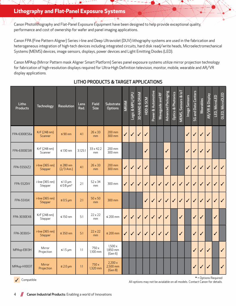
Lithography and Flat-Panel Exposure Systems
4 Canon Industrial Products: Enabling a world of Innovations
Litho Products Technology Resolution Lens
Red.FieldSize
Substrate Options M
RA
M
Logi
c &
MPU
/GPU
3D-N
AN
D &
DR
AM
HD
D &
SCM
Pow
er &
Aut
omot
ive
Wav
egui
de a
nd R
F
Adv
ance
d Pa
ckag
ing
Opt
ics
& P
hoto
nics
MEM
S, S
enso
rs &
IoT
Imag
e Se
nsor
s
5G a
nd D
ata
Cent
ers
Wea
rabl
es
AR
/VR
& D
ispl
ay
LED
, Mic
roLE
D
OLE
D, M
icro
OLE
D
FPA-6300ES6aKrF (248 nm)
Scanner≤ 90 nm 4:1
26 x 33 mm
200 mm300 mm 3 3 3 3 3 3 3 3
FPA-6300ESWKrF (248 nm)
Scanner≤ 130 nm 3.125:1
33 x 42.2 mm
200 mm300 mm 3 3 3 3 3 3
FPA-5550iZ2i-line (365 nm)
Stepper≤ 280 nm (2/3 Ann.)
4:126 x 33
mm200 mm300 mm 3 3 3 3 3 3 3 3 3 3 3
FPA-5520iVi-line (365 nm)
Stepper≤ 1.0 µm≤ 0.8 µm*
2:152 x 34
mm300 mm 3 3 3 3 3 3 3 3 3 3 3 3 3 3 3
FPA-5510iXi-line (365 nm)
Stepper≤ 0.5 µm 2:1
50 x 50 mm
300 mm 3 3 3 3 3 3 3 3 3 3 3 3
FPA-3030EX6KrF (248 nm)
Stepper≤ 150 nm 5:1
22 x 22 mm
≤ 200 mm 3 3 3 3 3 3 3 3 3 3 3
FPA-3030i5+i-line (365 nm)
Stepper≤ 350 nm 5:1
22 x 22 mm
≤ 200 mm 3 3 3 3 3 3 3 3 3 3 3
MPAsp-E813HMirror
Projection≤ 1.5 µm 1:1
750 x 1,100 mm
1,500 x 1,850 mm
(Gen 6)3 3 3 3
MPAsp-H1003TMirror
Projection≤ 2.0 µm 1:1
750 x 1,320 mm
2,200 x 2,500 mm
(Gen 8)3 3 3 3
LITHO PRODUCTS & TARGET APPLICATIONS
Canon Photolithography and Flat-Panel Exposure Equipment have been designed to help provide exceptional quality, performance and cost of ownership for wafer and panel imaging applications.
Canon FPA (Fine Pattern Aligner) Series i-line and Deep Ultraviolet (DUV) lithography systems are used in the fabrication and heterogeneous integration of high-tech devices including integrated circuits, hard disk read/write heads, Microelectromechanical Systems (MEMS) devices, image sensors, displays, power devices and Light Emitting Diodes (LED).
Canon MPAsp (Mirror Pattern mask Aligner Smart Platform) Series panel exposure systems utilize mirror projection technology for fabrication of high-resolution displays required for Ultra-High Definition television, monitor, mobile, wearable and AR/VR display applications.
3 Compatible* = Options Required
All options may not be avialable on all models. Contact Canon for details.
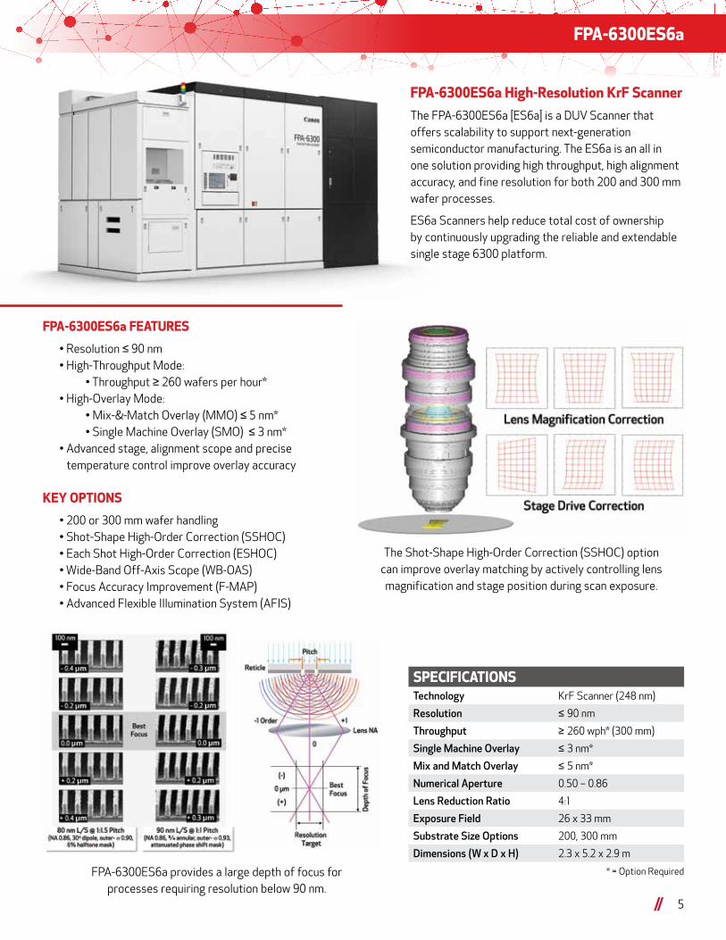
FPA-6300ES6a
5
FPA-6300ES6a FEATURES
• Resolution ≤ 90 nm • High-Throughput Mode: • Throughput ≥ 260 wafers per hour* • High-Overlay Mode: • Mix-&-Match Overlay (MMO) ≤ 5 nm* • Single Machine Overlay (SMO) ≤ 3 nm* • Advanced stage, alignment scope and precise temperature control improve overlay accuracy
KEY OPTIONS
• 200 or 300 mm wafer handling • Shot-Shape High-Order Correction (SSHOC) • Each Shot High-Order Correction (ESHOC) • Wide-Band Off-Axis Scope (WB-OAS) • Focus Accuracy Improvement (F-MAP) • Advanced Flexible Illumination System (AFIS)
FPA-6300ES6a High-Resolution KrF Scanner
The FPA-6300ES6a [ES6a] is a DUV Scanner that offers scalability to support next-generation semiconductor manufacturing. The ES6a is an all in one solution providing high throughput, high alignment accuracy, and fine resolution for both 200 and 300 mm wafer processes.
ES6a Scanners help reduce total cost of ownership by continuously upgrading the reliable and extendable single stage 6300 platform.
The Shot-Shape High-Order Correction (SSHOC) option can improve overlay matching by actively controlling lens magnification and stage position during scan exposure.
FPA-6300ES6a provides a large depth of focus for processes requiring resolution below 90 nm.
SPECIFICATIONSTechnology KrF Scanner (248 nm)
Resolution ≤ 90 nm
Throughput ≥ 260 wph* (300 mm)
Single Machine Overlay ≤ 3 nm*
Mix and Match Overlay ≤ 5 nm*
Numerical Aperture 0.50 – 0.86
Lens Reduction Ratio 4:1
Exposure Field 26 x 33 mm
Substrate Size Options 200, 300 mm
Dimensions (W x D x H) 2.3 x 5.2 x 2.9 m
* = Option Required
FPA-6300ESW
6 Canon Industrial Products: Enabling a world of Innovations
FPA-6300ESW FEATURES
• Lens Reduction 3.125:1 • Expanded field size from 26 x 33 mm to 33 x 42.2 mm • Flexible alignment solutions including alignment through multi-color RGB photo resist • Proven FPA-6300 Platform
KEY OPTIONS
• 200, 300 mm wafer handling • Wide-Band Off-Axis Scope (WB-OAS) • Advanced Flexible Illumination System (AFIS) • Focus Spot Automatic Chuck Cleaning • CD Uniformity Improvement • Standard Mechanical Interface Over Head Transport Kit (SMIF-OHT)
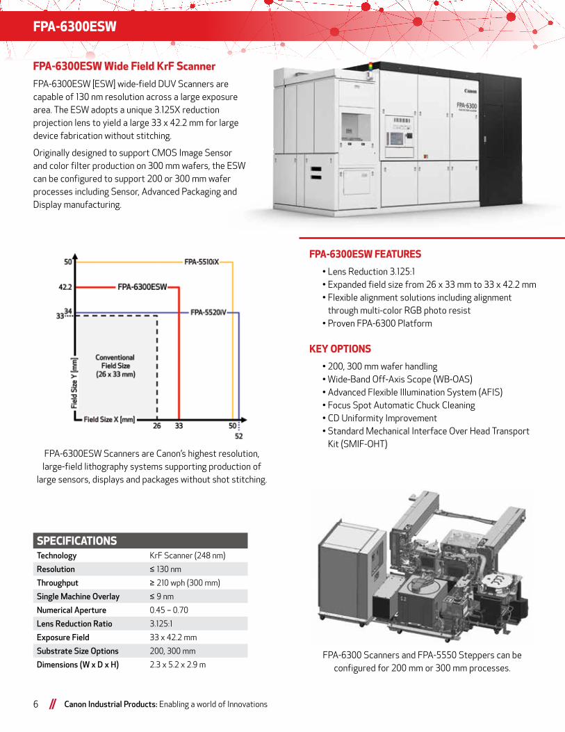
FPA-6300ESW Scanners are Canon’s highest resolution, large-field lithography systems supporting production of
large sensors, displays and packages without shot stitching.
FPA-6300 Scanners and FPA-5550 Steppers can be configured for 200 mm or 300 mm processes.
SPECIFICATIONSTechnology KrF Scanner (248 nm)
Resolution ≤ 130 nm
Throughput ≥ 210 wph (300 mm)
Single Machine Overlay ≤ 9 nm
Numerical Aperture 0.45 – 0.70
Lens Reduction Ratio 3.125:1
Exposure Field 33 x 42.2 mm
Substrate Size Options 200, 300 mm
Dimensions (W x D x H) 2.3 x 5.2 x 2.9 m
FPA-6300ESW Wide Field KrF Scanner
FPA-6300ESW [ESW] wide-field DUV Scanners are capable of 130 nm resolution across a large exposure area. The ESW adopts a unique 3.125X reduction projection lens to yield a large 33 x 42.2 mm for large device fabrication without stitching.
Originally designed to support CMOS Image Sensor and color filter production on 300 mm wafers, the ESW can be configured to support 200 or 300 mm wafer processes including Sensor, Advanced Packaging and Display manufacturing.
FPA-5550iZ2
7
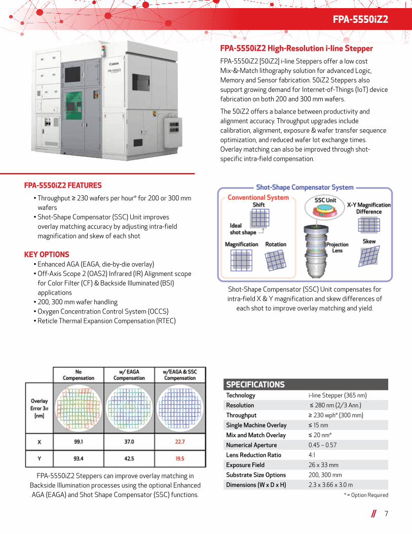
Shot-Shape Compensator (SSC) Unit compensates for intra-field X & Y magnification and skew differences of
each shot to improve overlay matching and yield.
FPA-5550iZ2 Steppers can improve overlay matching in Backside Illumination processes using the optional Enhanced AGA (EAGA) and Shot Shape Compensator (SSC) functions.
FPA-5550iZ2 FEATURES
• Throughput ≥ 230 wafers per hour* for 200 or 300 mm wafers • Shot-Shape Compensator (SSC) Unit improves overlay matching accuracy by adjusting intra-field magnification and skew of each shot
KEY OPTIONS • Enhanced AGA (EAGA, die-by-die overlay) • Off-Axis Scope 2 (OAS2) Infrared (IR) Alignment scope for Color Filter (CF) & Backside Illuminated (BSI) applications • 200, 300 mm wafer handling • Oxygen Concentration Control System (OCCS) • Reticle Thermal Expansion Compensation (RTEC)
FPA-5550iZ2 High-Resolution i-line Stepper
FPA-5550iZ2 [50iZ2] i-line Steppers offer a low cost Mix-&-Match lithography solution for advanced Logic, Memory and Sensor fabrication. 50iZ2 Steppers also support growing demand for Internet-of-Things (IoT) device fabrication on both 200 and 300 mm wafers.
The 50iZ2 offers a balance between productivity and alignment accuracy. Throughput upgrades include calibration, alignment, exposure & wafer transfer sequence optimization, and reduced wafer lot exchange times. Overlay matching can also be improved through shot-specific intra-field compensation.
SPECIFICATIONSTechnology i-line Stepper (365 nm)
Resolution ≤ 280 nm (2/3 Ann.)
Throughput ≥ 230 wph* (300 mm)
Single Machine Overlay ≤ 15 nm
Mix and Match Overlay ≤ 20 nm*
Numerical Aperture 0.45 – 0.57
Lens Reduction Ratio 4:1
Exposure Field 26 x 33 mm
Substrate Size Options 200, 300 mm
Dimensions (W x D x H) 2.3 x 3.66 x 3.0 m
* = Option Required
FPA-5520iV
8 Canon Industrial Products: Enabling a world of Innovations
FPA-5520iV Advanced Packaging i-line Stepper
FPA-5520iV [20iV] Steppers address next-generation Fan Out Wafer Level Packaging [FOWLP] challenges as demand for cost effective back-end high-resolution processes increases.
Available options supporting future FOWLP processes include the new High-Resolution (HR) Option that equips the 20iV with newly design projection lens with a maximum Numerical Aperture (NA) of 0.24. The 20iV-HR can provide 0.8 µm resolution patterning for high-density VIA and Redistribution Layer (RDL) processes.
20iV warpage compensation and die-by-die overlay options also support fabrication of multi-die Fan-Out packages by compensating for the substrate distortion and die-shift that is common in FOWLP processes.
FPA-5520iV FEATURES
• Resolution ≤ 0.8 um* • Lens Reduction 2:1 • Wide Field 52 x 34 mm • 20iV Steppers offer a wide exposure field, while balancing resolution and Depth of Focus (DoF) for thin and thick, positive and negative resist processes
KEY OPTIONS
• High-Resolution (HR) • Enhanced AGA (EAGA, die-by-die overlay) • Through Silicon Alignment (TSA) System • Resist Outgas Exhaust System • Wafer Warpage: Wafer Vacuum Assist (WVA)
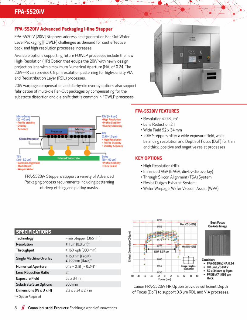
FPA-5520iV Steppers support a variety of Advanced Packaging process requirements including patterning
of deep etching and plating masks.
Canon FPA-5520iV HR Option provides sufficient Depth of Focus (DoF) to support 0.8 µm RDL and VIA processes.
* = Option Required
SPECIFICATIONSTechnology i-line Stepper (365 nm)
Resolution ≤ 1 µm (0.8 µm)*
Throughput ≥ 160 wph (300 mm)
Single Machine Overlay ≤ 150 nm (Front)≤ 500 nm (Back)*
Numerical Aperture 0.15 – 0.18 ( – 0.24)*
Lens Reduction Ratio 2:1
Exposure Field 52 x 34 mm
Substrate Size Options 300 mm
Dimensions (W x D x H) 2.3 x 3.34 x 2.7 m
FPA-5510iX
9
FPA-5510iX FEATURES
• Exposure Field 50 x 50 mm (max Φ 70.7 mm) • X max = 52 mm • Y max = 56 mm • Stepper Alignment Options enable overlay process optimization for Color Filter (CF) and Backside Illuminated (BSI) Processes
KEY OPTIONS
• Wide Band Off-Axis Scope (WB-OAS) • Oxygen Concentration Control System (OCCS) • Enhanced AGA (EAGA, die-by-die overlay) • 200, 300 mm wafer handling • Resist Outgas Exhaust System • PC Remote Console • Online Functions (GEM2, GEM0304)
FPA-5510iX Wide-Field, High-Resolution i-line Stepper
FPA-5510iX [10iX] Steppers provide high-resolution imaging across large exposure area and compatibility with a range of advanced functions. 10iX Steppers offer a large 50 x 50 mm exposure field allowing users to improve imaging performance and productivity by avoiding stitching of adjacent shots to expand field size.
Originally designed for image sensor Color Filter (CF) fabrication, the 10iX can be extended to provide high-resolution pattern for Field Programmable Gate Array (FPGA), Advanced Packaging, display and other large device applications.
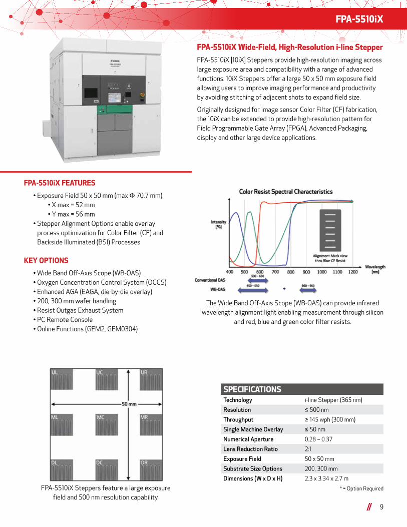
The Wide Band Off-Axis Scope (WB-OAS) can provide infrared wavelength alignment light enabling measurement through silicon
and red, blue and green color filter resists.
FPA-5510iX Steppers feature a large exposure field and 500 nm resolution capability.
* = Option Required
SPECIFICATIONSTechnology i-line Stepper (365 nm)
Resolution ≤ 500 nm
Throughput ≥ 145 wph (300 mm)
Single Machine Overlay ≤ 50 nm
Numerical Aperture 0.28 – 0.37
Lens Reduction Ratio 2:1
Exposure Field 50 x 50 mm
Substrate Size Options 200, 300 mm
Dimensions (W x D x H) 2.3 x 3.34 x 2.7 m
FPA-3030i5+
10 Canon Industrial Products: Enabling a world of Innovations
FPA-3030i5+ i-line Stepper for IoT and MEMS Devices
The FPA-3030i5+ [30i5+] Steppers deliver performance and flexibility required for manufacturing and R&D environments and support a variety of substrate materials, diameters and thicknesses.
The 30i5+ is able to support a range of innovative Internet-of-Things (IoT) applications and can configured to process wafers from 75 mm (3”) to 200 mm (8”) in diameter. 30i5+ systems can also be configured to handle two different wafer sizes with the Multi-Wafer Handling Kit option.
The resolution, overlay, productivity and available options of the 30i5+ make it a cost-effective solution for challenging ≤ 200 mm wafer processes.
FPA-3030i5+ FEATURES
• Resolution ≤ 350 nm • Lens Reduction 5:1 • Substrate handling capability: 75, 100, 150, 200 mm • FPA-3030i5+ Steppers leverage and extend proven Canon FPA-3000 Stepper designs
KEY OPTIONS
• Through Silicon Alignment (TSA) Scope • Multi-Wafer Size Handling Kit • 75 & 100 mm, 100 & 150 mm, 150 & 200 mm • Warped/Bonded/Transparent Wafer Handling • Enhanced AGA (EAGA, die-by-die overlay) • Canon Built-In Metrology (CanoMap) • Online Functions (GEM2, GEM0304)
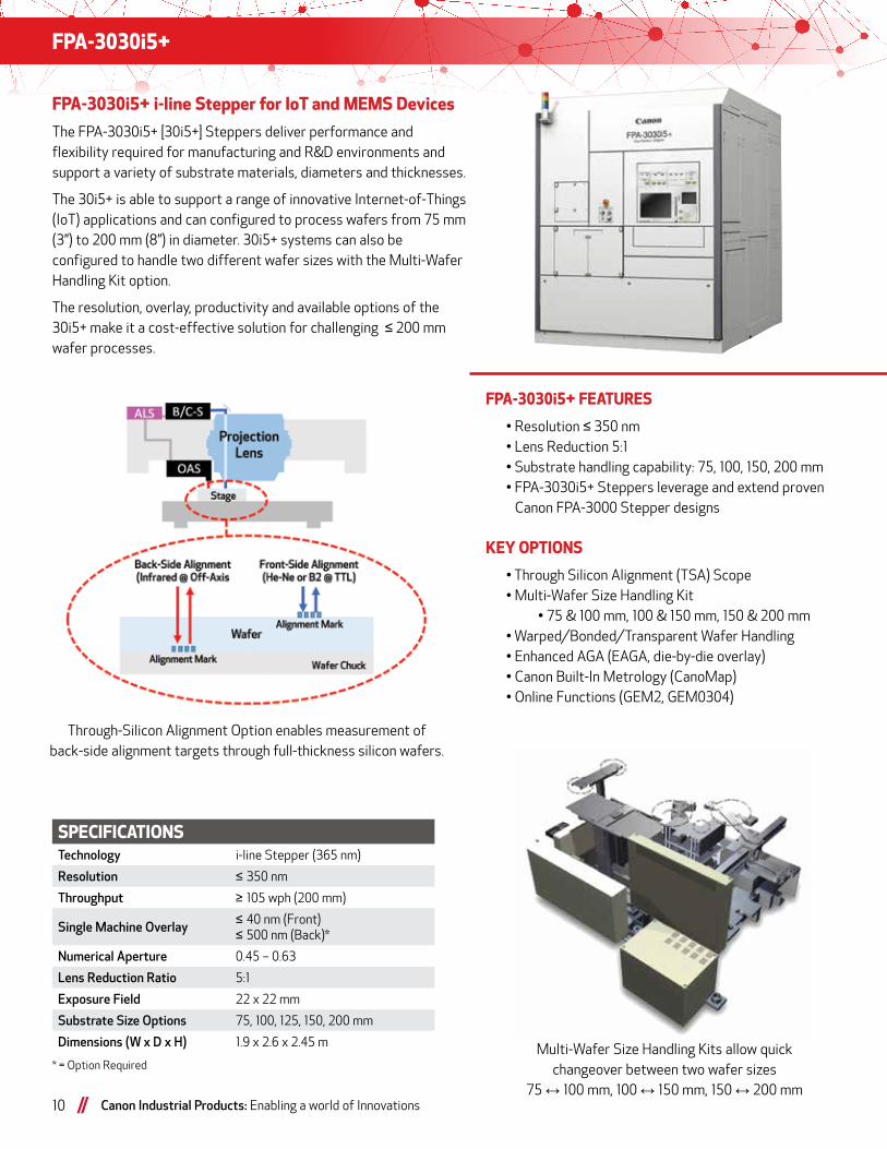
Through-Silicon Alignment Option enables measurement of back-side alignment targets through full-thickness silicon wafers.
Multi-Wafer Size Handling Kits allow quick changeover between two wafer sizes
75 ↔ 100 mm, 100 ↔ 150 mm, 150 ↔ 200 mm
* = Option Required
SPECIFICATIONSTechnology i-line Stepper (365 nm)
Resolution ≤ 350 nm
Throughput ≥ 105 wph (200 mm)
Single Machine Overlay ≤ 40 nm (Front) ≤ 500 nm (Back)*
Numerical Aperture 0.45 – 0.63
Lens Reduction Ratio 5:1
Exposure Field 22 x 22 mm
Substrate Size Options 75, 100, 125, 150, 200 mm
Dimensions (W x D x H) 1.9 x 2.6 x 2.45 m
FPA-3030EX6
11
FPA-3030EX6 FEATURES
• 248 nm exposure wavelength Stepper • Resolution ≤ 150 nm • Single Machine Overlay ≤ 25 nm • Substrate handling capability: 75, 100, 150, 200 mm • e-Console Software supports advanced automation and remote operation functions
KEY OPTIONS
• PC Remote Console • Through Silicon Alignment (TSA) Scope • Multi-Wafer Size Handling Kit • 75 & 100 mm, 100 & 150 mm, 150 & 200 mm • Warped/Bonded/Transparent Wafer Handling • Enhanced AGA (EAGA, die-by-die overlay) • Canon Internal Metrology (CanoMap)
FPA-3030EX6
FPA-3030EX6 [30EX6] Deep UV (DUV) Steppers, provide a low cost alternative to Scanners for aggressive customers seeking high-resolution imaging. The EX6 can also be configured to handle different substrate materials, sizes and thicknesses required for fabricating advanced analog, sensor, RF and power devices as well as emerging Internet-of-Things (IoT) applications with special wafer requirements.
FPA-3030EX6 Steppers offer the highest level of performance among KrF (Krypton Fluoride) Excimer Laser Steppers and are a long-term solution for growing industry demands.
FPA-303EX6 DUV (KrF, 248 nm) Steppers provide cost-efficient high-resolution imaging on ≤ 200 mm substrates for sensor, power and IoT applications.
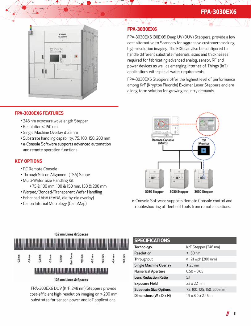
e-Console Software supports Remote Console control and troubleshooting of fleets of tools from remote locations.
SPECIFICATIONSTechnology KrF Stepper (248 nm)
Resolution ≤ 150 nm
Throughput ≥ 121 wph (200 mm)
Single Machine Overlay ≤ 25 nm
Numerical Aperture 0.50 – 0.65
Lens Reduction Ratio 5:1
Exposure Field 22 x 22 mm
Substrate Size Options 75, 100, 125, 150, 200 mm
Dimensions (W x D x H) 1.9 x 3.0 x 2.45 m
12 Canon Industrial Products: Enabling a world of Innovations
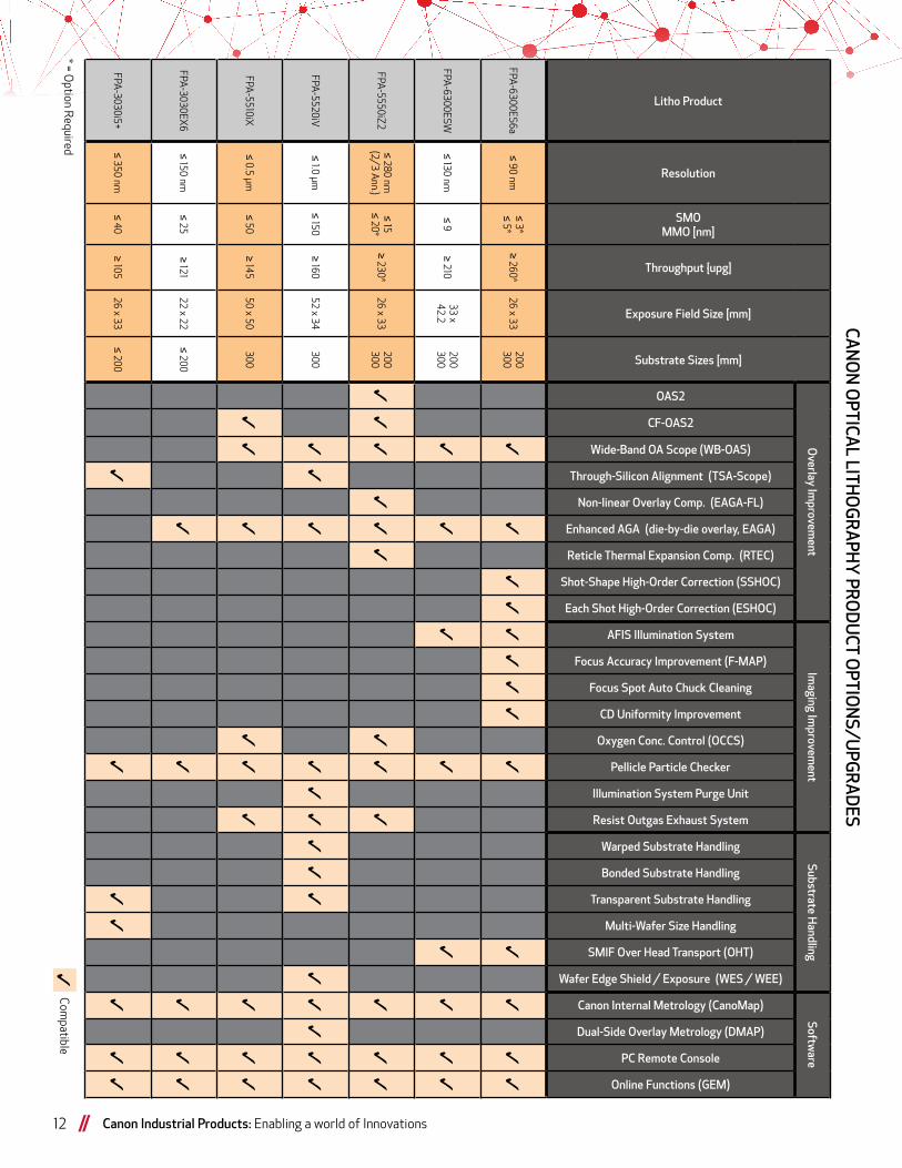
Litho Product
Resolution
SMOMMO [nm]
Throughput {upg]
Exposure Field Size [mm]
Substrate Sizes [mm]
Overlay Im
provement
Imaging Im
provement
Substrate Handling
Software
OAS2
CF-OAS2
Wide-Band OA Scope (WB-OAS)
Through-Silicon Alignment (TSA-Scope)
Non-linear Overlay Comp. (EAGA-FL)
Enhanced AGA (die-by-die overlay, EAGA)
Reticle Thermal Expansion Comp. (RTEC)
Shot-Shape High-Order Correction (SSHOC)
Each Shot High-Order Correction (ESHOC)
AFIS Illumination System
Focus Accuracy Improvement (F-MAP)
Focus Spot Auto Chuck Cleaning
CD Uniformity Improvement
Oxygen Conc. Control (OCCS)
Pellicle Particle Checker
Illumination System Purge Unit
Resist Outgas Exhaust System
Warped Substrate Handling
Bonded Substrate Handling
Transparent Substrate Handling
Multi-Wafer Size Handling
SMIF Over Head Transport (OHT)
Wafer Edge Shield / Exposure (WES / WEE)
Canon Internal Metrology (CanoMap)
Dual-Side Overlay Metrology (DMAP)
PC Remote Console
Online Functions (GEM)
FPA-6300ES6a
≤ 90 nm≤ 3*≤ 5*
≥ 260*26 x 33
200300
33
33
33
33
33
33
3
FPA-6300ESW
≤ 130 nm≤ 9
≥ 21033 x 42.2
200300
33
33
33
33
FPA-5550iZ
2≤ 280 nm
(2/3 A
nn.)≤ 15≤ 20*
≥ 230*26 x 33
200300
33
33
33
33
33
33
FPA-5520iV
≤ 1.0 µm≤ 150
≥ 16052 x 34
3003
33
33
33
33
33
33
3
FPA-5510iX
≤ 0.5 µm≤ 50
≥ 14550 x 50
3003
33
33
33
33
FPA-3030EX
6≤ 150 nm
≤ 25≥ 121
22 x 22≤ 200
33
33
3
FPA-3030i5+
≤ 350 nm≤ 40
≥ 10526 x 33
≤ 2003
33
33
33
3C
ompatible
* = Option R
equired
CAN
ON
OPTICA
L LITHO
GR
APH
Y PR
OD
UCT O
PTION
S/UPG
RA
DES
Canon Nanoimprint Lithography
FPA-1200NZ2C Wafer Imprint System
FPA-1200NZ2C [NZ2C] NIL cluster tools has been introduced in semiconductor memory mass production lines. NZ2C NIL systems are designed to enable semiconductor manufacturing of circuit patterns as small as 10 nm.
NIL process equipment uses an array of Piezo actuators to apply mag correction and localized intra-field heat
input to improve overlay matching accuracy.
FPA-1100NR2 Mask Replication System
FPA-1100NR2 [NR2] Nanoimprint Lithography (NIL) systems are the world’s first mass-production equipment designed for nanoimprint mask replication. NR2 Mask Replication Systems duplicate lithography masks utilizing low-cost NIL technology.
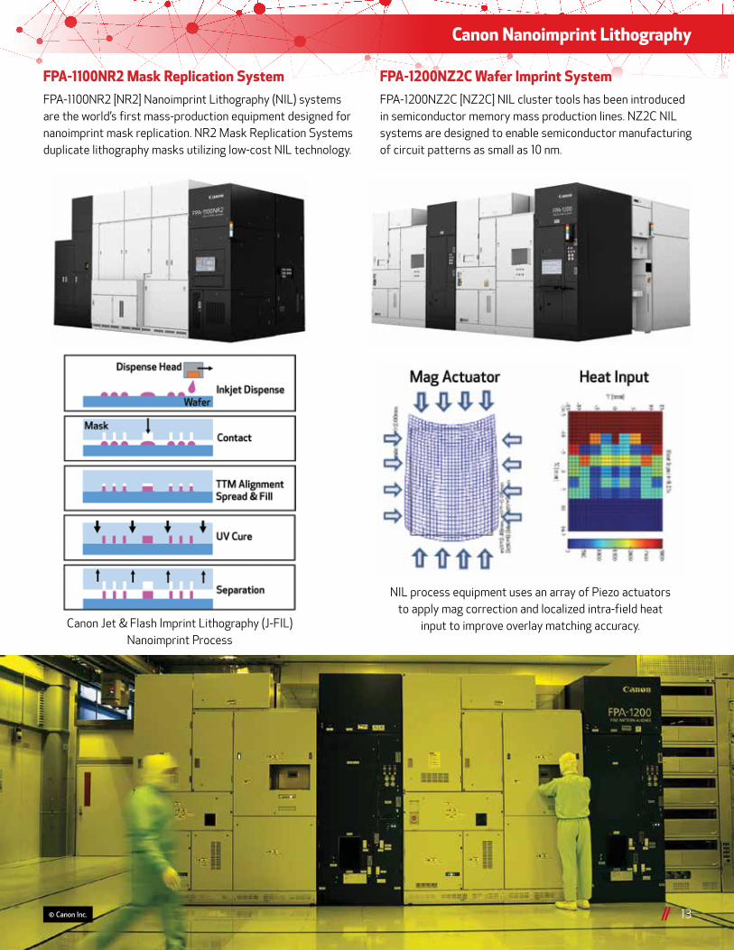
Canon Jet & Flash Imprint Lithography (J-FIL) Nanoimprint Process
© Canon Inc. 13
MPAsp Flat-Panel Exposure Systems
14 Canon Industrial Products: Enabling a world of Innovations
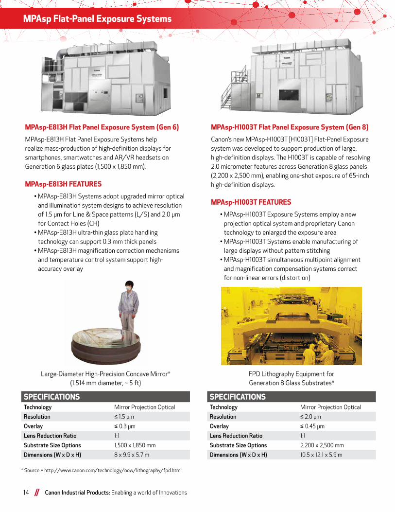
MPAsp-E813H Flat Panel Exposure System (Gen 6)
MPAsp-E813H Flat Panel Exposure Systems help realize mass-production of high-definition displays for smartphones, smartwatches and AR/VR headsets on Generation 6 glass plates (1,500 x 1,850 mm).
MPAsp-E813H FEATURES
• MPAsp-E813H Systems adopt upgraded mirror optical and illumination system designs to achieve resolution of 1.5 µm for Line & Space patterns (L/S) and 2.0 µm for Contact Holes (CH) • MPAsp-E813H ultra-thin glass plate handling technology can support 0.3 mm thick panels • MPAsp-E813H magnification correction mechanisms and temperature control system support high- accuracy overlay
Large-Diameter High-Precision Concave Mirror* (1.514 mm diameter, ~ 5 ft)
FPD Lithography Equipment for Generation 8 Glass Substrates*
* Source = http://www.canon.com/technology/now/lithography/fpd.html
MPAsp-H1003T Flat Panel Exposure System (Gen 8)
Canon’s new MPAsp-H1003T [H1003T] Flat-Panel Exposure system was developed to support production of large, high-definition displays. The H1003T is capable of resolving 2.0 micrometer features across Generation 8 glass panels (2,200 x 2,500 mm), enabling one-shot exposure of 65-inch high-definition displays.
MPAsp-H1003T FEATURES
• MPAsp-H1003T Exposure Systems employ a new projection optical system and proprietary Canon technology to enlarged the exposure area • MPAsp-H1003T Systems enable manufacturing of large displays without pattern stitching • MPAsp-H1003T simultaneous multipoint alignment and magnification compensation systems correct for non-linear errors (distortion)
SPECIFICATIONSTechnology Mirror Projection Optical
Resolution ≤ 1.5 µm
Overlay ≤ 0.3 µm
Lens Reduction Ratio 1:1
Substrate Size Options 1,500 x 1,850 mm
Dimensions (W x D x H) 8 x 9.9 x 5.7 m
SPECIFICATIONSTechnology Mirror Projection Optical
Resolution ≤ 2.0 µm
Overlay ≤ 0.45 µm
Lens Reduction Ratio 1:1
Substrate Size Options 2,200 x 2,500 mm
Dimensions (W x D x H) 10.5 x 12.1 x 5.9 m
Canon ANELVA Physical Vapor Deposition (PVD), Etch Systems and Components
15
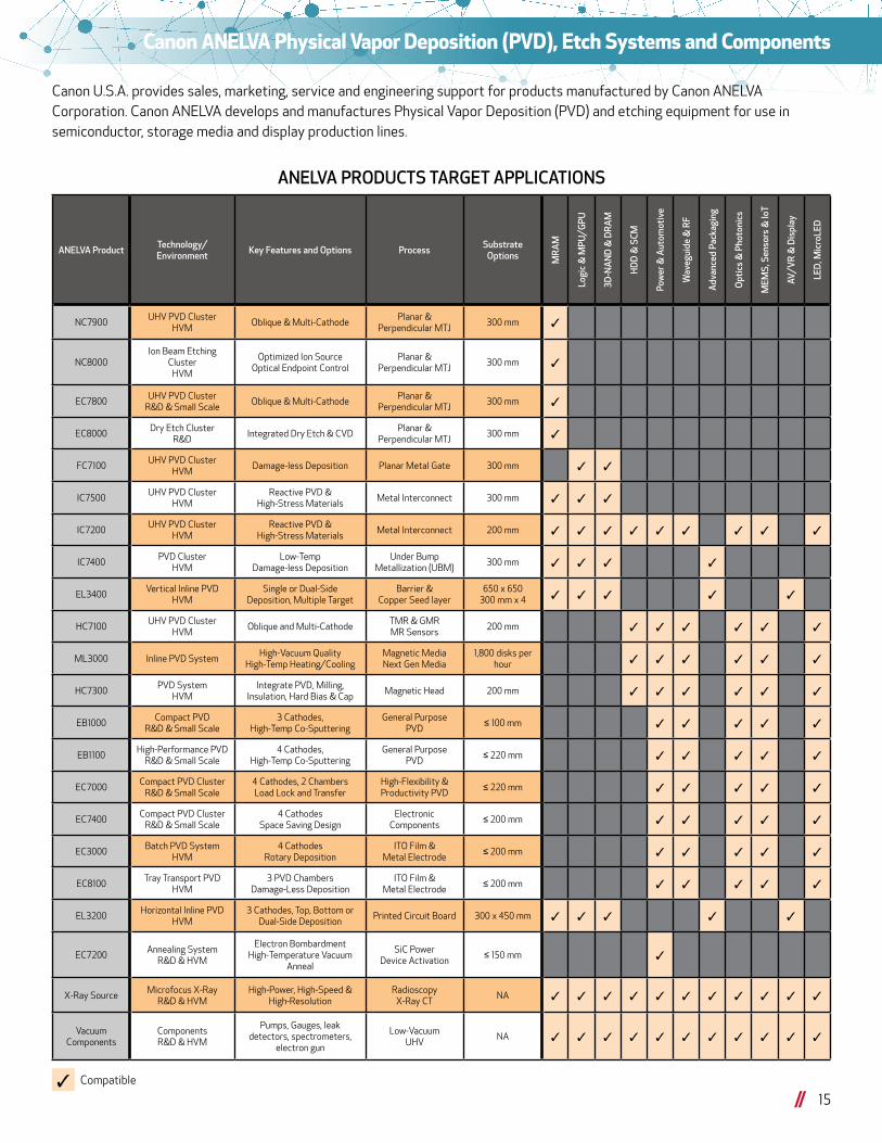
Canon U.S.A. provides sales, marketing, service and engineering support for products manufactured by Canon ANELVA Corporation. Canon ANELVA develops and manufactures Physical Vapor Deposition (PVD) and etching equipment for use in semiconductor, storage media and display production lines.
ANELVA PRODUCTS TARGET APPLICATIONS
ANELVA Product Technology/Environment Key Features and Options Process Substrate
Options MR
AM
Logi
c &
MPU
/GPU
3D-N
AN
D &
DR
AM
HD
D &
SCM
Pow
er &
Aut
omot
ive
Wav
egui
de &
RF
Adv
ance
d Pa
ckag
ing
Opt
ics
& P
hoto
nics
MEM
S, S
enso
rs &
IoT
AV/V
R &
Dis
play
LED
, Mic
roLE
D
NC7900UHV PVD Cluster
HVMOblique & Multi-Cathode
Planar & Perpendicular MTJ
300 mm 3
NC8000Ion Beam Etching
ClusterHVM
Optimized Ion SourceOptical Endpoint Control
Planar & Perpendicular MTJ
300 mm 3
EC7800UHV PVD Cluster
R&D & Small ScaleOblique & Multi-Cathode
Planar & Perpendicular MTJ
300 mm 3
EC8000Dry Etch Cluster
R&DIntegrated Dry Etch & CVD
Planar & Perpendicular MTJ
300 mm 3
FC7100UHV PVD Cluster
HVMDamage-less Deposition Planar Metal Gate 300 mm 3 3
IC7500UHV PVD Cluster
HVMReactive PVD &
High-Stress MaterialsMetal Interconnect 300 mm 3 3 3
IC7200UHV PVD Cluster
HVMReactive PVD &
High-Stress MaterialsMetal Interconnect 200 mm 3 3 3 3 3 3 3 3 3
IC7400PVD Cluster
HVMLow-Temp
Damage-less DepositionUnder Bump
Metallization (UBM)300 mm 3 3 3 3
EL3400Vertical Inline PVD
HVMSingle or Dual-Side
Deposition, Multiple TargetBarrier &
Copper Seed layer650 x 650
300 mm x 4 3 3 3 3 3
HC7100UHV PVD Cluster
HVMOblique and Multi-Cathode
TMR & GMR MR Sensors
200 mm 3 3 3 3 3 3
ML3000 Inline PVD SystemHigh-Vacuum Quality
High-Temp Heating/CoolingMagnetic MediaNext Gen Media
1,800 disks per hour 3 3 3 3 3 3
HC7300PVD System
HVMIntegrate PVD, Milling,
Insulation, Hard Bias & CapMagnetic Head 200 mm 3 3 3 3 3 3
EB1000Compact PVD
R&D & Small Scale3 Cathodes,
High-Temp Co-SputteringGeneral Purpose
PVD≤ 100 mm 3 3 3 3 3
EB1100High-Performance PVD
R&D & Small Scale4 Cathodes,
High-Temp Co-SputteringGeneral Purpose
PVD≤ 220 mm 3 3 3 3 3
EC7000Compact PVD Cluster
R&D & Small Scale4 Cathodes, 2 ChambersLoad Lock and Transfer
High-Flexibility & Productivity PVD
≤ 220 mm 3 3 3 3 3
EC7400Compact PVD Cluster
R&D & Small Scale4 Cathodes
Space Saving DesignElectronic
Components≤ 200 mm 3 3 3 3 3
EC3000Batch PVD System
HVM4 Cathodes
Rotary DepositionITO Film &
Metal Electrode≤ 200 mm 3 3 3 3 3
EC8100Tray Transport PVD
HVM3 PVD Chambers
Damage-Less DepositionITO Film &
Metal Electrode≤ 200 mm 3 3 3 3 3
EL3200Horizontal Inline PVD
HVM3 Cathodes, Top, Bottom or
Dual-Side DepositionPrinted Circuit Board 300 x 450 mm 3 3 3 3 3
EC7200Annealing System
R&D & HVM
Electron BombardmentHigh-Temperature Vacuum
Anneal
SiC Power Device Activation
≤ 150 mm 3
X-Ray SourceMicrofocus X-Ray
R&D & HVMHigh-Power, High-Speed &
High-ResolutionRadioscopy
X-Ray CTNA 3 3 3 3 3 3 3 3 3 3 3
Vacuum Components
Components R&D & HVM
Pumps, Gauges, leak detectors, spectrometers,
electron gun
Low-VacuumUHV
NA 3 3 3 3 3 3 3 3 3 3 3
3 Compatible
Canon ANELVA Semiconductor Manfacturing Equipment
16 Canon Industrial Products: Enabling a world of Innovations
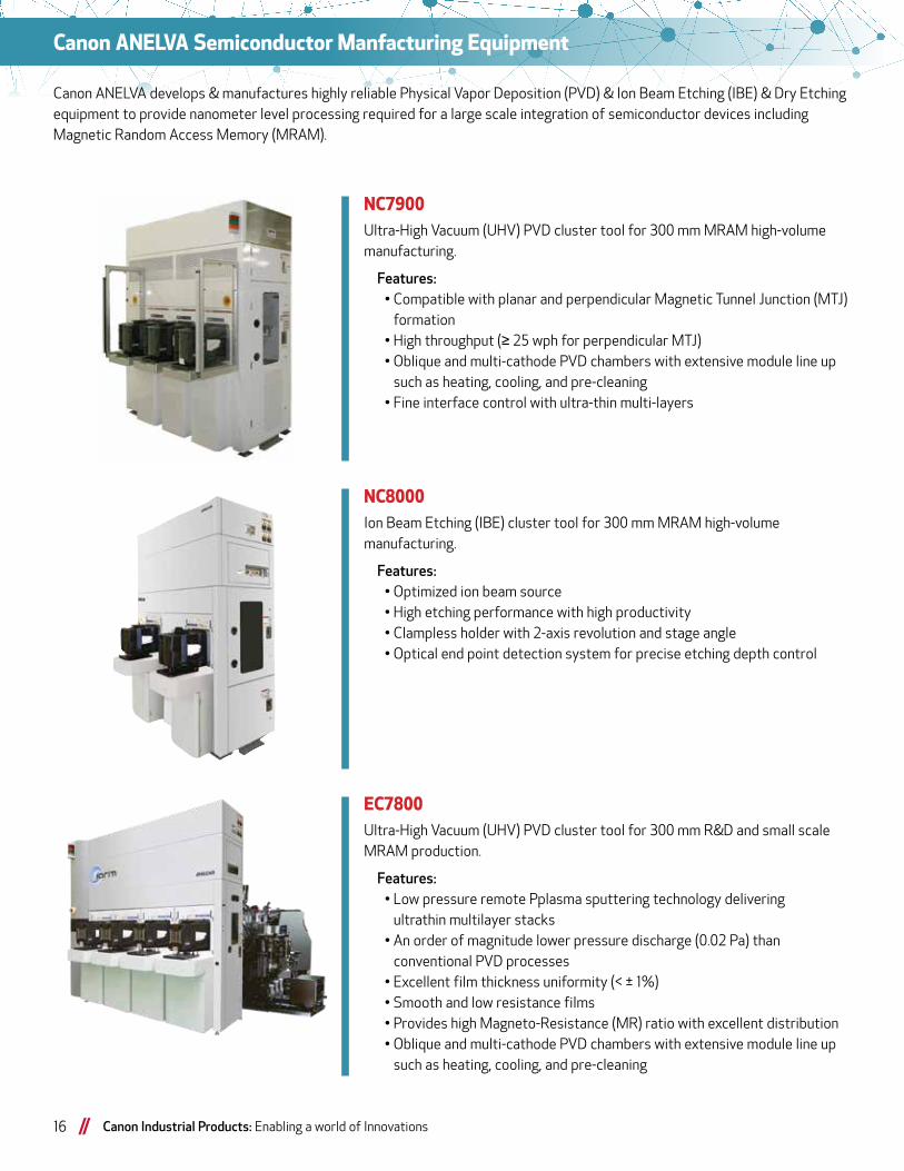
Canon ANELVA develops & manufactures highly reliable Physical Vapor Deposition (PVD) & Ion Beam Etching (IBE) & Dry Etching equipment to provide nanometer level processing required for a large scale integration of semiconductor devices including Magnetic Random Access Memory (MRAM).
NC7900Ultra-High Vacuum (UHV) PVD cluster tool for 300 mm MRAM high-volume manufacturing.
Features: • Compatible with planar and perpendicular Magnetic Tunnel Junction (MTJ) formation • High throughput (≥ 25 wph for perpendicular MTJ) • Oblique and multi-cathode PVD chambers with extensive module line up such as heating, cooling, and pre-cleaning • Fine interface control with ultra-thin multi-layers
NC8000Ion Beam Etching (IBE) cluster tool for 300 mm MRAM high-volume manufacturing.
Features: • Optimized ion beam source • High etching performance with high productivity • Clampless holder with 2-axis revolution and stage angle • Optical end point detection system for precise etching depth control
EC7800Ultra-High Vacuum (UHV) PVD cluster tool for 300 mm R&D and small scale MRAM production.
Features: • Low pressure remote Pplasma sputtering technology delivering ultrathin multilayer stacks • An order of magnitude lower pressure discharge (0.02 Pa) than conventional PVD processes • Excellent film thickness uniformity (< ± 1%) • Smooth and low resistance films • Provides high Magneto-Resistance (MR) ratio with excellent distribution • Oblique and multi-cathode PVD chambers with extensive module line up such as heating, cooling, and pre-cleaning
17
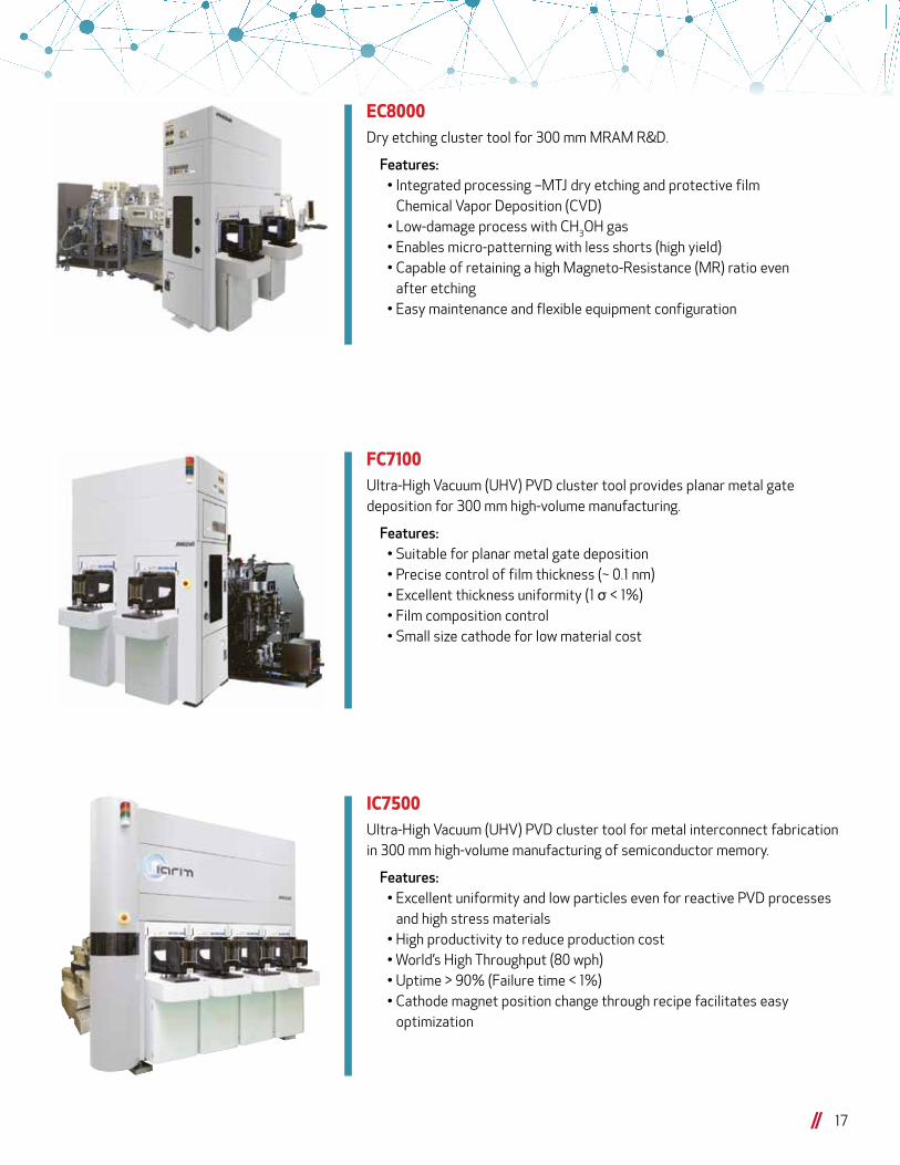
EC8000Dry etching cluster tool for 300 mm MRAM R&D.
Features: • Integrated processing –MTJ dry etching and protective film Chemical Vapor Deposition (CVD) • Low-damage process with CH3OH gas • Enables micro-patterning with less shorts (high yield) • Capable of retaining a high Magneto-Resistance (MR) ratio even after etching • Easy maintenance and flexible equipment configuration
FC7100Ultra-High Vacuum (UHV) PVD cluster tool provides planar metal gate deposition for 300 mm high-volume manufacturing.
Features: • Suitable for planar metal gate deposition • Precise control of film thickness (~ 0.1 nm) • Excellent thickness uniformity (1 σ < 1%) • Film composition control • Small size cathode for low material cost
IC7500Ultra-High Vacuum (UHV) PVD cluster tool for metal interconnect fabrication in 300 mm high-volume manufacturing of semiconductor memory.
Features: • Excellent uniformity and low particles even for reactive PVD processes and high stress materials • High productivity to reduce production cost • World’s High Throughput (80 wph) • Uptime > 90% (Failure time < 1%) • Cathode magnet position change through recipe facilitates easy optimization
18 Canon Industrial Products: Enabling a world of Innovations
IC7200
Ultra-High Vacuum (UHV) PVD cluster tool for metal interconnect processes in 200 mm high-volume manufacturing of semiconductor memory.
Features: • High reliability 200 mm cluster tool • Excellent uniformity and low particles even for reactive PVD processes and high stress materials • Cathode magnet position change through recipe facilitates easy optimization • Add-on options for step coverage improvement and plasma damage reduction
IC7400
PVD cluster tool for Under Bump Metallization (UBM) processes in 300 mm high-volume memory packaging.
Features: • Used by leading suppliers of 300 mm UBM processes • Stress control • Low temperature deposition • Damage-less deposition • Improved adhesion • Easy to customize hardware
EL3400
Panel PVD System for Advance Packaging applications including barrier and Copper seed deposition.
Features: • Vertical linear transport system • Compatible with various substrates (Si, glass, organic, …) • Large deposition area (� 650 mm x 2 panels, Φ 300 mm x 8 wafers, � 300 mm x 8 panels) • Moisture control • Plasma surface activation for superior adhesion • Single side or double side deposition • Multiple targets for multilayer deposition
Canon ANELVA Storage and Hard Disk Drive Manufacturing Equipment
19
Canon ANELVA commands the world’s largest market share of the PVD equipment used for production of high density magnetic heads & disks for use in PCs & servers. Using proprietary technology, Canon ANELVA intends to continue our technology leadership in the evolution of hard disk drives & innovative storage media.
HC7100
200 mm PVD cluster tool production of MagnetoResistive (MR) magnetic sensors.
Features: • Compatible with Tunnel Magneto-Resistance (TMR) and Giant Magneto-Resistance (GMR) processes • An order of magnitude lower pressure discharge (0.02 Pa) than conventional PVD processes • Excellent film thickness uniformity (< ± 1%) • Smooth and low resistance films • Provides high Magneto-Resistance (MR) ratio with excellent distribution • Oblique and multi-cathode PVD chambers with extensive module line up such as heating, cooling, and pre-cleaning
ML3000
Inline PVD tool for R&D & mass production of next generation Hard Disk Drive (HDD) magnetic media.
Features: • High productivity (up to 1,800 disks/hr) with a 90 m2 footprint • Over 10 days of continuous operation is possible • Emphasis on vacuum (~ 10-6 Pa) quality to improve magnetic characteristics of media • High temperature heating and cooling units for the development of next generation thermally assisted magnetic recording media
HC7300
PVD tool for Hard Disk Drive (HDD) magnetic head production.
Features: • Effectively consolidates magnetic head production processes – milling Ô insulator Ô hard bias Ô cap layer • Module lineup enables optimum shape required by read element (IBE, anisotropic deposition, isotropic deposition, RIE, etc…) • Excellent deposition characteristic and high productivity
Canon ANELVA Electronic Device Manufacturing Equipment
20 Canon Industrial Products: Enabling a world of Innovations
Canon ANELVA’s versatile device lineup supports next generation technology development and manufacturing of thin film devices such as Light Emitting Diodes (LEDs), CMOS Image Sensors, Compound Semiconductors, Piezoelectric Devices, and Power Devices.
EB1000
Compact and flexible PVD system for ≤ 100 mm general purpose R&D applications.
Features: • Three Φ 2” compact cathodes • Various deposition geometries (offset rotation, static) by tray transport • Supports substrates up to Φ 100 mm • High temperature (800 °C) substrate heating (option) • Load lock chamber (option) • Ternary co-sputtering (option) • Auto-pumping and manual transportation/deposition operation • Space saving design (standard footprint W 1.8 m x D 1.1 m x H 1.55 m)
EB1100
High-performance PVD system for ≤ 220 mm R&D and small scale production.
Features: • Fully automated operation • Supports up to four Φ 4” cathodes • Supports substrates up to Φ 220 mm • Various deposition geometries (offset rotation, static) by tray transport • High temperature (800 °C) substrate heating (option) • Space saving unit body design (standard footprint W 1.45 m x D 1.6 m x H 1.85 m) • Co-sputtering (option)
EC7000 SERIES
Compact PVD cluster system for ≤ 220 mm R&D and small scale production of LEDs, Compound Semiconductors, and Power Devices.
Features: • Equipped with load lock stocker chamber and transfer chamber • Supports up to two sputtering chambers • Fully automated operation • Supports up to four Φ 4” cathodes • Supports substrates up to Φ 220 mm • Various deposition geometries (offset rotation, static) by tray transport • High temperature (800 °C) substrate heating (option) • Space saving unit body design (standard footprint W 1.45 m x D 2.3 m x H 1.85 m) • Co-sputtering (option)
EC7400
Compact cluster tool for ≤ 200 mm production of electronic components such as SAW Filters, TC-SAW Filters, Piezoelectric Devices, and Power Devices.
Features: • Fully automated operation • Able to accommodate a variety of process modules according to requirements • High target utilization
• Substrate size up to Φ 200 mm • Up to four Φ 7.1” cathodes • Space saving design
21
EL3000 SERIES
Batch type PVD system for LED production.
Features: • Ideal for Indium Tin Oxide (ITO) transparent conductive film deposition, metal electrode film deposition, etc. • Rotary deposition facilitates batch processing of multiple wafers and good uniformity • Fully automated operation • Supports substrates up to Φ 200 mm • Tray transport (50 Φ 2” wafers/batch) • Supports up to four Φ 7.1” or Φ 12.5” cathodes • High target utilization to help reduce cost • Customizable configuration according to application and production volume
EC8100
Tray Transport PVD cluster system for small wafer and LED production.
Features: • Ideal for Indium Tin Oxide (ITO) transparent conductive film deposition, metal electrode film deposition, etc. • Long distance sputtering • Excellent uniformity over large area • Multiple wafers deposition per batch (four Φ 8”, eight Φ 6”, etc.) • High target utilization • Fully automated operation • Up to three sputtering chambers
EL3200
Horizontal linear transport PVD system for production of electronic components such as Sensor Devices.
Features: • Configurable for single side or dual-side deposition according to production volume • Supports laminated films by using up to 3 (single side) cathodes • Can accommodate up to 25 trays in the stocker chamber • Pre-heating chamber (Option) • 300 mm x 450 mm effective deposition area
EC7200
Electron Bombardment vacuum annealing tool for SiC power device activation in ≤ 150 mm R&D and mass production.
Features: • High temperature (up to 1850 °C) process for implant activation • In situ carbon capping for low surface roughness • Clean vacuum • Cluster tool configuration that supports up to three annealing chambers • Substrate size up to Φ 6” • Excellent repeatability (sheet resistance uniformity ± 4.9% @ 1,000 runs) • High electrical activation, low sheet resistance, reduction of diode leakage current, and low surface roughness
Canon ANELVA Components
22 Canon Industrial Products: Enabling a world of Innovations
Thin-Film manufacturers and R&D facilities use Canon ANELVA vacuum components as virtually indispensable parts in systems incorporating vacuum technology. Canon ANELVA vacuum technology contributes to stable operation of equipment and measuring instruments.
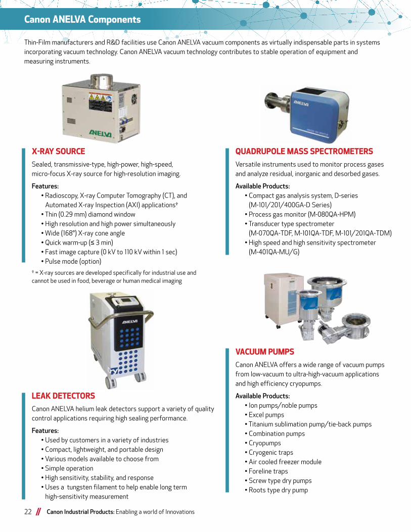
X-RAY SOURCE
Sealed, transmissive-type, high-power, high-speed, micro-focus X-ray source for high-resolution imaging.
Features: • Radioscopy, X-ray Computer Tomography (CT), and Automated X-ray Inspection (AXI) applications† • Thin (0.29 mm) diamond window • High resolution and high power simultaneously • Wide (168°) X-ray cone angle • Quick warm-up (≤ 3 min) • Fast image capture (0 kV to 110 kV within 1 sec) • Pulse mode (option)
† = X-ray sources are developed specifically for industrial use and cannot be used in food, beverage or human medical imaging
VACUUM PUMPS
Canon ANELVA offers a wide range of vacuum pumps from low-vacuum to ultra-high-vacuum applications and high efficiency cryopumps.
Available Products: • Ion pumps/noble pumps • Excel pumps • Titanium sublimation pump/tie-back pumps • Combination pumps • Cryopumps • Cryogenic traps • Air cooled freezer module • Foreline traps • Screw type dry pumps • Roots type dry pump
QUADRUPOLE MASS SPECTROMETERS
Versatile instruments used to monitor process gases and analyze residual, inorganic and desorbed gases.
Available Products: • Compact gas analysis system, D-series (M-101/201/400GA-D Series) • Process gas monitor (M-080QA-HPM) • Transducer type spectrometer (M-070QA-TDF, M-101QA-TDF, M-101/201QA-TDM) • High speed and high sensitivity spectrometer (M-401QA-MU/G)
LEAK DETECTORS
Canon ANELVA helium leak detectors support a variety of quality control applications requiring high sealing performance.
Features: • Used by customers in a variety of industries • Compact, lightweight, and portable design • Various models available to choose from • Simple operation • High sensitivity, stability, and response • Uses a tungsten filament to help enable long term high-sensitivity measurement
23
VACUUM PARTS
Canon ANELVA offers various high quality ancillary vacuum parts to support your vacuum systems.
Available Products: • Ultra-High Vacuum (UHV) flange • Fittings and adaptors with ICF flange • Quick release couplings • Vacuum switch • UHV view ports • Sheathed heater and moly paste
VACUUM FEEDTHROUGHS
Vacuum Feedthroughs can be used to introduce rotary and/or linear motion to a device installed in vacuum.
Available Products: • Magnetic Coupling Type Rotary Feedthrough • Bellows Type Rotary Feedthrough • Linear Feedthrough • R/L Feedthrough • Current Terminal
VACUUM VALVES
Canon ANELVA offers a variety of vacuum valves.
Available Products: • UHV Type-L All-metal Valve • UHV Type-L Polyimide Valve • “V Series” Roughing pump valve V-025RV • “V Series” Type-L Valves V-040LV/ V-065LV/ V-100LV • UHV Variable Leak Valve • Inlet valve • Leak valve • Isolate Valve V-025SV • UHV Gate Valve MSB Series • UHV Gate Valve STD Series
VACUUM GAUGES AND CONTROLLERS
Canon ANELVA offers a diverse lineup of gauges to meet a variety of application requirements.
Available Products: • Cold Cathode Gauge (M-370CG) • Cold Cathode Pirani Gauge (M-361CP) • Capacitance Diaphragm Gauge (M-342DG) • Pirani Gauge (M-350PG) • Corrosion-resistant Pirani Gauge (M-351PG) • Ion Gauge (M-311HG) • Crystal Ion Gauge (M-336MX) • Crystal Gauge (M-320XG) • Wide Range Ionization Vacuum Gauges (M-431HG, M-833HG) • Ionization Vacuum Gauge (M-723HG, M-823HG, M-923HG) • Thermocouple Vacuum Gauge (M-012DM) • Miniature Gauge (MG-2, MG-2M, MG-2F, MG-2/WF) • Vacuum Gauge (Shultz, B-A, Nude Ion, Pirani, Thermocouple)
Canon Optomechatronics Products
24 Canon Industrial Products: Enabling a world of Innovations
OPTOELECTRONICS
Canon Optoelectronics integrate optical and electronic technologies with precise fabrication to produce a line of products for advanced R&D and production.
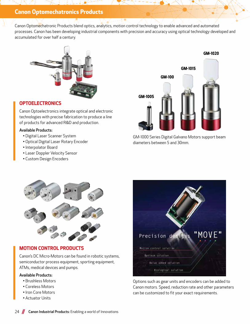
Available Products: • Digital Laser Scanner System • Optical Digital Laser Rotary Encoder • Interpolator Board • Laser Doppler Velocity Sensor • Custom Design Encoders
GM-1000 Series Digital Galvano Motors support beam diameters between 5 and 30mm.
MOTION CONTROL PRODUCTS
Canon’s DC Micro-Motors can be found in robotic systems, semiconductor process equipment, sporting equipment, ATMs, medical devices and pumps.
Available Products: • Brushless Motors • Coreless Motors • Iron Core Motors • Actuator Units
Canon Optomechatronic Products blend optics, analytics, motion control technology to enable advanced and automated processes. Canon has been developing industrial components with precision and accuracy using optical technology developed and accumulated for over half a century.
Options such as gear units and encoders can be added to Canon motors. Speed, reduction rate and other parameters can be customized to fit your exact requirements.
GM-1005
GM-100
GM-1015
GM-1020
25
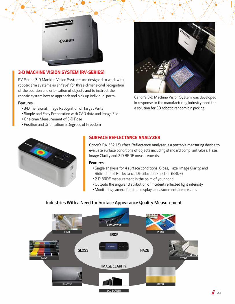
3-D MACHINE VISION SYSTEM (RV-SERIES)
RV-Series 3-D Machine Vision Systems are designed to work with robotic arm systems as an “eye” for three-dimensional recognition of the position and orientation of objects and to instruct the robotic system how to approach and pick up individual parts.
Features: • 3-Dimensional, Image Recognition of Target Parts • Simple and Easy Preparation with CAD data and Image File • One-time Measurement of 3-D Pose • Position and Orientation: 6 Degrees of Freedom
SURFACE REFLECTANCE ANALYZER
Canon’s RA-532H Surface Reflectance Analyzer is a portable measuring device to evaluate surface conditions of objects including standard compliant Gloss, Haze, Image Clarity and 2-D BRDF measurements.
Features: • Single analysis for 4 surface conditions: Gloss, Haze, Image Clarity, and Bidirectional Reflectance Distribution Function (BRDF) • 2-D BRDF measurement in the palm of your hand • Outputs the angular distribution of incident reflected light intensity • Monitoring camera function displays measurement area results
Canon’s 3-D Machine Vision System was developed in response to the manufacturing industry need for a solution for 3D robotic random bin picking.
BRDF
GLOSS HAZE
IMAGE CLARITY
STONEPAINT
METALPLASTIC
FILM
AUTOMOTIVE
LCD SCREEN
Industries With a Need for Surface Appearance Quality Measurement
Canon Industrial Products Markets
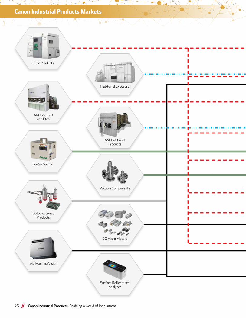
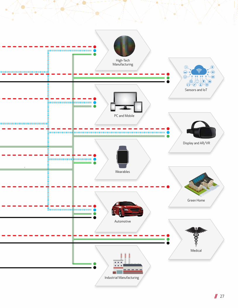
26 Canon Industrial Products: Enabling a world of Innovations
Litho Products
Flat-Panel Exposure
ANELVA PanelProducts
X-Ray Source
Surface ReflectanceAnalyzer
ANELVA PVD and Etch
Vacuum Components
OptoelectronicProducts
3-D Machine Vision
DC Micro Motors
27
Sensors and IoT
PC and Mobile
High-TechManufacturing
Industrial Manufacturing
Display and AR/VR
Wearables
Medical
Automotive
Green Home

CANON U.S.A., INC.Industrial Products Division3300 North 1st Street • San Jose, CA 95134TEL: 1-408-468-2000 • Email: [email protected]/industrial
Canon is registered trademark of Canon Inc. in the United States, and may also be registered trademarks or trademarks in other countries. ANELVA is a registered trademark of Canon Anelva Corporation in the United States, and may also be a registered trademark or trademark in other countries. All other referenced product names and marks are trademarks of their respective owners. Specifications and availability subject to change. Not responsible for typographical errors.©2019 Canon U.S.A., Inc. All rights reserved. 2/2019
Related Documents