CALIFORNIA STATE UNIVERSITY, NORTHRIDGE STUDY ON DETERMINATION OF AN ANALYTICAL MODEL FOR THE BARRIER HEIGHT ENHANCEMENT OF THE GaN SCHOTTKY BARRIER DIODE USING LOW-ENERGY ION IMPLANTATION A graduate project submitted in partial fulfillment of the requirements For the degree of Masters of Science In Electrical Engineering. By Avinash Babu Paleru December 2012

Welcome message from author
This document is posted to help you gain knowledge. Please leave a comment to let me know what you think about it! Share it to your friends and learn new things together.
Transcript
CALIFORNIA STATE UNIVERSITY, NORTHRIDGE
STUDY ON DETERMINATION OF AN ANALYTICAL MODEL FOR THE
BARRIER HEIGHT ENHANCEMENT OF THE GaN SCHOTTKY BARRIER
DIODE USING LOW-ENERGY ION IMPLANTATION
A graduate project submitted in partial fulfillment of the requirements
For the degree of Masters of Science
In Electrical Engineering.
By
Avinash Babu Paleru
December 2012
The graduate project of Avinash Babu Paleru is approved:
Dr. Radmanesh Matthew M Date
Dr. Cable Vaughn P Date
Dr. Chattopadhyay Somnath, Chair Date
California State University, Northridge
ii
ACKNOWLEDGEMENT
This project would not have been possible without the support of many people. I
wish to express my gratitude to my major supervisor, Dr. Chattopadhyay Somnath who
was abundantly helpful and offered invaluable assistance, support and guidance. I would
also like to thank my other committee members, Dr. Radmanesh Matthew M and Dr.
Cable Vaughn P for providing their valuable suggestions.
I would also like to thank the Department of Electrical and Computer Engineering
for providing the facilities to complete this project.
Finally, I would like to express my love and gratitude to my parents for their
understanding and endless love, through the duration of my studies.
iii
TABLE OF CONTENTS
SIGNATURE PAGE ii
ACKNOWLEDGEMENT iii
LIST OF FIGURES vi
LIST OF TABLES vii
ABSTRACT viii
CHAPTER 1.0 INTRODUCTION 01
CHAPTER 2.0 GaN MATERIAL 11
2.1 INTRODUCTION 11
2.2 NITRIDE EPITAXIAL GROWTH TECHNIQUES 11
2.2.1 HYDRIDE VAPOR PHASE EPITAXY 11
2.2.2 METAL ORGANIC CHEMICAL VAPOR DEPOSITION 12
2.2.2.1 ATMOSPHERIC PRESSURE MOCVD 13
2.2.2.2 LOW PRESSURE MOCVD 14
2.2.2.3 PLASMA ASSISTED MOVCD 15
2.2.3 MOLECULAR BEAM EPITAXY 16
2.2.3.1 MBE GROWTH TECHNIQUES 17
2.2.3.2 THE STRENGTHS OF MBE 18
2.3 FACTORS INFLUENCING GaN CRYSTALLINE QUALITY 19
2.3.1 SUBSTRATES 19
2.3.2 BUFFER LAYER 22
2.4 OVERVIEW OF METAL GaN CONTACT TECHNIQUES 23
2.4.1 OHMIC CONTACT ON GaN 23
2.4.2SCHOTTKY CONTACT ON GaN 24
CHAPTER 3.0 SCHOTTKY DIODE 26
3.1 GaN SCHOTTKY DIODE 28
3.2 SEMI-TRANSPARENT GaN SCHOTTKY DIODE 28
3.3 ITO/N-GaAS SCHOTTKY PHOTO DIODES 29
3.4 DIODE FABRICATION 31
iv
3.4.1 GROWN JUNCTION DIODE 31
3.4.2 ALLOW TYPED OR FUSED JUNCTION DIODE 31
3.4.3 DIFFUSION JUNCTION DIODE 32
3.4.4 PLANAR DIFFUSED DIODE 33
3.4.5 POINT CONTACT DIODE 33
CHAPTER 4.0 EXTRACTING THE PARAMETERS 35
4.1 BASIC THEORETCAL DERIVATIONS 35
4.2 INTERFACIAL MODEL FOR THE BARRIER HEIGHT
ENHANCEMENT 39
CHAPTER 5.0 NUMERICAL RESULTS & EXPERIMENTAL COMPARISIONS 43
CHAPTER 6.0 CONCLUSIONS 48
REFERENCES 49
APPENDIX A 54
APPENDIX B 56
v
LIST OF FIGURES
Figure 1.1: INSPEC & ACTIVITIES OF GAN OVER YEARS 06
Figure 2.1 VAPOR TRANSPORT GAN REACTOR 12
Figure 2.2: MOVCD GROTH REACTOR 12
Figure 2.3: TWO FLOW MOVCD 14
Figure 2.4: VERTICAL ROTATING LP-MOVCD 14
Figure 2.5: PLASMA ASSISTED MOCVD 15
Figure 2.6: MBE GROWTH CHAMBER 16
Figure 2.7: SURFACE PROCESSING DURING MBE SYSYTEM 18
Figure 2.8: BARRIER HEIGHT vs WORKFUNCTION 25
Figure 3.1: INTERNAL STRUCTURE OF SCHOTTKY DIODE 26
Figure 3.2: SCHOTTKY DIODE SYMBOL 27
Figure 3.3: GaN MESFET STRUCTURE 28
Figure 3.4: GaN WITH SEMI TRANSPARENT SCHOTTKY CONTACT 29
Figure 3.5: GaAs SCHOTTKY PHOTO DIODE 30
Figure 3.6: FUSION JUNCTION DIODE 31
Figure 3.7: DIFFUSION JUNCTION DIODE 32
Figure 3.8: PLANAR DIFFUSED DIODE 33
Figure 4.1 A: DOPING PROFILE OF THE IMPLANTED SUBSTRATE 35
Figure 4.1 B: IMPLANTED SCHOTTKY DIODE AT THERMAL POSITION 36
Figure 5.1: BARRIER HEIGHT ENHANCEMENT vs ION DOSE 44
Figure 5.2: BARRIER HEIGHT INCREM ENT vs ION DOSE 45
Figure 5.3: BARRIER HEIGHT vs ION DOSE 46
vi
LIST OF TABLES
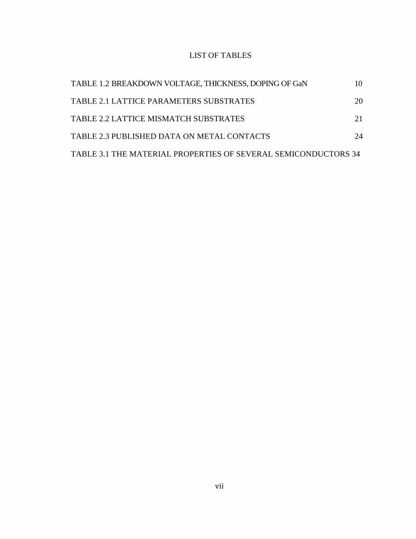
TABLE 1.2 BREAKDOWN VOLTAGE, THICKNESS, DOPING OF GaN 10
TABLE 2.1 LATTICE PARAMETERS SUBSTRATES 20
TABLE 2.2 LATTICE MISMATCH SUBSTRATES 21
TABLE 2.3 PUBLISHED DATA ON METAL CONTACTS 24
TABLE 3.1 THE MATERIAL PROPERTIES OF SEVERAL SEMICONDUCTORS 34
vii
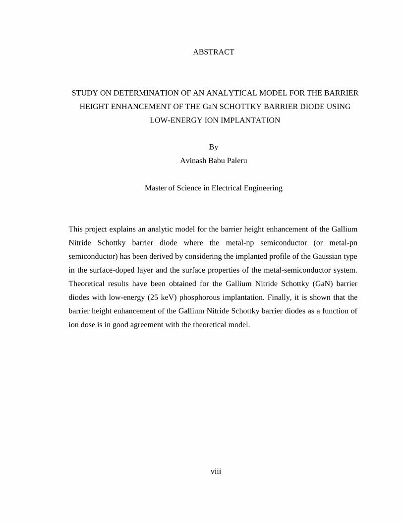
ABSTRACT
STUDY ON DETERMINATION OF AN ANALYTICAL MODEL FOR THE BARRIER
HEIGHT ENHANCEMENT OF THE GaN SCHOTTKY BARRIER DIODE USING
LOW-ENERGY ION IMPLANTATION
By
Avinash Babu Paleru
Master of Science in Electrical Engineering
This project explains an analytic model for the barrier height enhancement of the Gallium
Nitride Schottky barrier diode where the metal-np semiconductor (or metal-pn
semiconductor) has been derived by considering the implanted profile of the Gaussian type
in the surface-doped layer and the surface properties of the metal-semiconductor system.
Theoretical results have been obtained for the Gallium Nitride Schottky (GaN) barrier
diodes with low-energy (25 keV) phosphorous implantation. Finally, it is shown that the
barrier height enhancement of the Gallium Nitride Schottky barrier diodes as a function of
ion dose is in good agreement with the theoretical model.
viii
CHAPTER 1
INTRODUCTION
In recent years, Gallium Nitride has received increased attention because of its
potential for a wide variety of high-power devices. Gallium Nitride (GaN) is a binary III/V
direct band gap semiconductor familiarly used in bright light-emitting diodes since the
1990s. The compound is relatively hard material that has a Wurtzite crystal structure. Its
wide band gap of 3.4 eV affords it to possess special properties for applications in high
power, optoelectronic and high-frequency devices. For instance, GaN is the substrate
which makes violet (405 nm) laser diodes to be possible, without the use of nonlinear
optical frequency-doubling.
GaN sensitivity to ionizing radiation is very low as other group nitrides III,
making it suitable material for solar cell arrays for satellites. Space and military
applications also benefits as these devices have shown stability in radiation environments.
As Gallium Nitride (GaN) transistors can operate at much higher temperatures and work at
much higher voltages than gallium arsenide (GaAs) transistors, this make them ideal power
amplifiers at microwave frequencies.
GaN is a hard, mechanically stable wide band gap semiconductor material
with high heat capacity and thermal conductivity. In its pure form GaN resists cracking and
can be deposited in thin film on silicon carbide or sapphire, irrespective of the mismatch in
their lattice constants. GaN can be doped with oxygen or Silicon (Si) with oxygen to form
n-type and with magnesium (Mg) to form p-type. However the Si and Mg atoms change
the way as the GaN crystals grow in the processes, introducing tensile stresses and making
them brittle. GaN compounds also tend to have a high spatial defect frequency, on the
order of hundred million to ten billion defects per square centimeter.
High quality crystalline GaN can be obtained by low temperature deposited
buffer layer technology. This high quality crystalline GaN led to the discovery of p n
junction blue/UV LED’s, p type GaN and room-temperature stimulated emission
(indispensable for laser action).
1
This has made to the commercialization of high performance blue LEDs and long lifetime
violet laser diodes, and to the development of nitride-based devices such as high-speed
field-effect transistors and UV detectors.
High brightness GaN light emitting diodes (LED's) have completed the range of primary
colors and then made to drove the applications such as daylight visible full color LED
displays then white LEDs and blue laser devices were possible. The first generation GaN
depended high brightness LEDs were using a thin film of GaN deposited via MOCVD on
Silicon Carbide/Sapphire. The other substrates used are zinc oxide and with lattice constant
mismatch of only 2%, and of silicon carbide (SiC). Group III nitride semiconductors are in
general recognized as one of the most promising semiconductor family for fabricating
optical devices in the UV and visible short wavelength region [9].
The high electron mobility, saturation velocity and very high breakdown voltages of
GaN has also made it an ideal candidate for high power and high temperature microwave
applications, evidenced by GaN's high Johnson's Figure of Merit. Potential markets for
high power or high frequency devices based on GaN include microwave radio-frequency
power amplifiers used in high speed wireless data transmission and high voltage switching
devices used for power grids. The potential mass market application for GaN based RF
transistors is the microwave source for microwave ovens, replacing the magnetrons which
are currently used. Large band gap means that the performance of GaN transistors is
maintained up to higher temperatures than silicon transistors. The first GaN metal/oxide
semiconductor field effect transistors (GaN MOSFET) were experimentally demonstrated
in the year 1993 and they are still being actively developed [9].
GaN devices have also had initial success as RF switching devices, generally at lower
voltages than those of SiC. Manufacturers grow the GaN devices on sapphire substrates,
involving high manufacturing costs. The breakthrough for GaN came with the ability to
grow GaN structures on silicon. Initial GaN-on-silicon devices all operated at less than
100V, targeting use in the data com-power-conversion market. GaN’s higher switching
speed and efficiency allows dc/dc converters to operate in the megahertz region, saving
2
space, reducing the need for heat sinks, and conserving power. International Rectifier was
the first company to offer GaN-on-silicon power switching devices to the commercial
market with the introduction of the IP2010 in early 2010. The device has a blocking
voltage of 20 to 40V and targets point-of-load dc/dc converters. The company’s
technology operates in depletion, normally on, mode but hides this characteristic from
designers because the company offers the parts as complete driver stages rather than as
discrete devices. For example, rather than quote a blocking voltage for the FETs,
International Rectifier quotes the GaN power stage by its input-voltage range of 7 to
13.2V, output voltage of 0.6 to 5.5V, output current of 30A, and operating frequency as
high as 3 MHz [10].
EPC (Efficient Power Conversion) also offers GaN devices, for which it uses
the trademarked name eGaN (enhanced-mode GaN). Recently introduced EPC2010 FET,
which has a drain-to-source voltage of 200V, a maximum on-resistance of 25 mΩ with 5V
applied to the gate, and a pulsed-current rating of 60A. Unlike International Rectifier’s
GaN power-conversion-stage device, the EPC2010 is a discrete transistor. The drive is
similar to a silicon power MOSFET, but some challenges in driving one exist. For
example, because of the high switching frequencies, an eGaN circuit is sensitive to layout.
The device also tolerates only a narrow range of gate voltages. To ensure that it’s on
requires 4.5V, but it can tolerate only 6V. Considering the power transients you can expect
in a power-converter environment, 1.5V is a narrow range of operation. Because the
threshold is lower, you must drive it even harder when the gate gets close to ground to
ensure that it stays below 1.4V rather than the 2.5V threshold you would encounter in a
silicon MOSFET.“There’s no reverse recovery loss, which is a performance gain. But
when you do leave the FET on, it still has a forward drop of greater than 1.5V, so you have
to be careful about dead time. None of these drawbacks are insurmountable, but have to be
careful” [10].
In the year 2010 the first enhancement mode GaN transistors became available.
These devices were designed to replace power MOSFETs in applications at which
switching speed or power conversion efficiency is critical. These type transistors also
called as eGaN FETs, were built by growing a thin layer of GaN on top of a standard
3
Silicon processed wafer. This allows the eGaN FETs to maintain costs similar to silicon
power MOSFETs, with the difference in superior electrical performance of GaN. GaN
violet laser diodes are used to read Blu ray Discs. Doping with a suitable transition metal
like manganese, GaN is one of the promising spintronics material (magnetic
semiconductors). The mixture of GaN with Al (AlGaN) or In (InGaN) with a band gap
dependent on ratio of Al or In to GaN allows the manufacture of light-emitting diodes
(LEDs) with colors that go from red to blue. GaN HEMTs have being offered
commercially from 2006, and have found immediate use in various wireless infrastructure
applications due to their high voltage operation and high efficiency [8].
The second generation technology with shorter gate lengths will be addressing
aerospace applications and higher frequency telecom. GaN based MESFET and MOSFET
transistors also offer many advantages in high power electronics, especially in electric car
and automotive applications. Nan tubes of GaN are proposed for applications in
optoelectronic, biochemical sensing and nano scale electronics applications. They were
also useful in military electronics like Active Electronically Scanned Array radars. GaN is
found to be biocompatible. This has lead to the implants of electrodes and electronics in
living organisms.
GaN crystals can be grown from a molten Na/Ga melt held under 100 atm pressure of
N2 at a temperature of 750° C. Here Ga will not react with N2 below 1000°C , the powder
must be made from some material that is more reactive, specifically in one of the following
ways:
2 Ga + 2 NH3 → 2 GaN + 3 H2 (1)
Ga2O3 + 2 NH3 → 2 GaN + 3 H2O (2)
Dust form of GaN is an irritant to eyes, skin and lungs. The environment health and safety
aspects of gallium nitride sources (such as trimethyl-gallium and ammonia) and industrial
hygiene monitoring studies of MOVPE sources have been reported recently in most of the
reviews. Finally GaN has been found to be non toxic.
4
The III-V nitrides have long been viewed as a promising system for
semiconductor devices operating in the blue and ultra-violet spectra region. In III-V
nitrides family, AlN, GaN, InN and their alloys are all wide bandgap semiconductor
materials, and can crystallize in both wurtzite and zinc-blende polytypes. The wurtzite
polytypes of GaN, AlN and InN form a continuous alloy system whose direct bandgap
cover from 1.9 eV for InN, to 3.4 eV for GaN, to 6.2 eV for AlN. Following recent
studies, the InN bandgap was found to be smaller than 0.8 eV [9]. These findings further
span the whole nitrides bandgap from infra-red into deep ultra-violet (UV) regions.
This makes the nitride system attractive for optoelectronic device applications,
such as light emitting diodes (LEDs), laser diodes (LDs) and photo detectors.High
t e m p e r a t u r e /high power/high frequency electronics is another area receiving
enormous attention for III-V nitrides. Presently, Si and GaAs are the two most widely
used materials in the semiconductor industries. Electronics devices based on current Si
and GaAs semiconductor technologies are not able to operate at elevated temperatures due
to the uncontrolled generation of intrinsic carriers. On the other hand, the wide
bandgap nature of nitrides such as GaN is attractive for high temperature
applications, because their intrinsic properties are maintained at much higher
temperatures. This suggests that GaN-based power devices can operate with less cooling
and fewer high cost processing steps associated with complicated structures designed to
maximize heat extraction. In addition, the III-V nitrides posses higher breakdown electric
field which sustains larger voltage gradient, enabling thinner active regions, lower on
resistances and high voltage operation as well as high electron drift velocity which leads to
faster operating speed.Other superior properties of nitrides include large piezoelectric
constants and possibility of passivation by forming thin layers of Ga2O3 or Al2O3
as well as high bonding energy. GaN has a bond energy of 8.92 eV/atom, InN 7.72
eV/atom, and AlN 11.52 eV/atom; giving high mechanical strength, chemical inertness
and radiation resistance. Moreover, nitride materials are non-toxic, environmentally
friendly materials compared to other conventional III-V compounds such as GaAs and
GaP which contain arsenic and phosphorous, and therefore are toxic to humans [11].
5
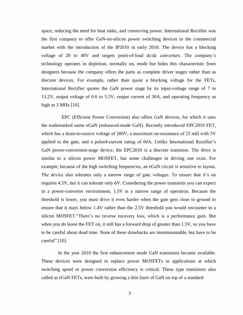
Researchers have labored for more than 35 years and have been able to
determine many of the physical parameters and properties of the III-V nitride
semiconductors. Among all the nitride semiconductors, GaN is by far the most heavily
studied [9].
HISTORICAL DEVELOPMENT OF NITRIDES
The evolution of nitride semiconductors has been interesting and followed a
difficult road. GaN was first synthesized by Johnson in which ammonia was passed over
hot gallium [11]. This technique produced small needles and platelets. Grimmeiss used
similar method to produce small GaN crystal for the purpose of measuring
photoluminescence spectra.
In 1969, Maruska and Tietjen succeeded in growing the first single- crystal GaN
on a sapphire substrate by using hydride vapor phase epitaxy (HVPE) technique. They
found that GaN posseses a direct transition band structure with bandgap energy of about
3.39 eV [11].
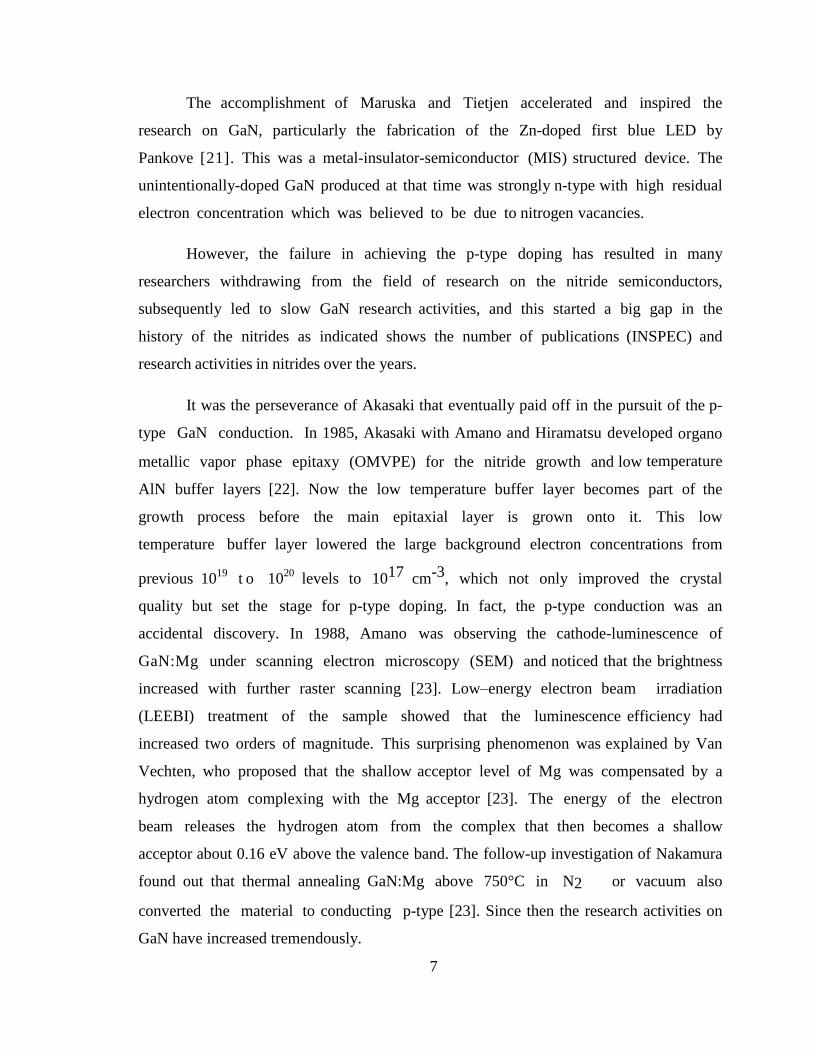
Fig. 1.1 Number of publications (INSPEC) and activities in GaN over the years
(adapted from Akasaki, 2002)
6
The accomplishment of Maruska and Tietjen accelerated and inspired the
research on GaN, particularly the fabrication of the Zn-doped first blue LED by
Pankove [21]. This was a metal-insulator-semiconductor (MIS) structured device. The
unintentionally-doped GaN produced at that time was strongly n-type with high residual
electron concentration which was believed to be due to nitrogen vacancies.
However, the failure in achieving the p-type doping has resulted in many
researchers withdrawing from the field of research on the nitride semiconductors,
subsequently led to slow GaN research activities, and this started a big gap in the
history of the nitrides as indicated shows the number of publications (INSPEC) and
research activities in nitrides over the years.
It was the perseverance of Akasaki that eventually paid off in the pursuit of the p-
type GaN conduction. In 1985, Akasaki with Amano and Hiramatsu developed organo
metallic vapor phase epitaxy (OMVPE) for the nitride growth and low temperature
AlN buffer layers [22]. Now the low temperature buffer layer becomes part of the
growth process before the main epitaxial layer is grown onto it. This low
temperature buffer layer lowered the large background electron concentrations from
previous 1019
t o 1020 levels to 1017 cm-3, which not only improved the crystal
quality but set the stage for p-type doping. In fact, the p-type conduction was an
accidental discovery. In 1988, Amano was observing the cathode-luminescence of
GaN:Mg under scanning electron microscopy (SEM) and noticed that the brightness
increased with further raster scanning [23]. Low–energy electron beam irradiation
(LEEBI) treatment of the sample showed that the luminescence efficiency had
increased two orders of magnitude. This surprising phenomenon was explained by Van
Vechten, who proposed that the shallow acceptor level of Mg was compensated by a
hydrogen atom complexing with the Mg acceptor [23]. The energy of the electron
beam releases the hydrogen atom from the complex that then becomes a shallow
acceptor about 0.16 eV above the valence band. The follow-up investigation of Nakamura
found out that thermal annealing GaN:Mg above 750°C in N2 or vacuum also
converted the material to conducting p-type [23]. Since then the research activities on
GaN have increased tremendously.
7
In recent years, the miniaturization of electronic devices has been drastically
enforced in the semiconductor technology. Knowledge on the microscopic electronic
properties of thin film becomes very important. On the other hand, the crystalline
microstructure is a fundamental property of the semiconductor.
The microstructure is closely related to the growth condition, it has a significant
influence on the quality of the film and the performance of the electronics devices
eventually. The detailed characterizations will be able to provide useful information about
the quality of the GaN films, so that some precautions can be employed during the
growth of the GaN and groundwork therefore is laid to optimize the growth conditions,
which will lead to improvement of the quality of the films.
GaN-based materials have been investigated intensively in recent years due to their
potential applications in visible and UV LEDs and LDs for lighting and data storage,
field effect transistors (FETs) for high-temperature and high-power electronics devices,
and solar-blind UV detectors [24]. These exciting applications present numerous
challenges in making high quality metal contacts to GaN-based materials, which is
crucial for device performances. Generally, making low-resistance ohmic contacts is
difficult for GaN-based materials, particularly p-type GaN due to difficulty in doping.
This difficulty has been one of the major obstacles in fabricating highly efficient LED
and LDs. Moreover, conventional metallization schemes may not have the adequate
thermal stability when devices operate at high power and high temperature
environments [24].
Porous semiconductors have drawn great deal of attention in recent years,
primarily due to the potential for intentional engineering of properties not readily
obtained in the corresponding crystalline precursors as well as the potential
applications in chemical and biochemical sensing. Porous semiconductors are also
under study as possible templates for epitaxial growth in which the pores could act as
sinks for mismatch dislocations and accommodate elastic strain in heterostructures, this
eventually leads to the growth of high quality epitaxial films with low structural defect
density and strain [25]. Interest in porous semiconductors also arises from the potential
applications in optoelectronics area.
8
Porous semiconductors have been demonstrated to be capable of shifting the
emission wavelength and enhancing the luminescence efficiency as compared to the un
etched precursors. Among porous semiconductors, porous silicon receives enormous
attention and has been investigated most intensively. However, the instability of the
physical property has prevented it from large scale application. This leads to the
development of porous semiconductors, for instances, the conventional III-V
compounds such as GaAs, GaP and InP, however, low band gap semiconductors
always suffer from the generation of charge carriers due to undesirable background
optical or thermal excitation. The research in porous GaN is strongly driven by the wide
band gap and superior physical properties such as the excellent thermal, mechanical and
chemical stability, nevertheless, the study of porous GaN is still in the stage of infancy.
Since porous GaN is a new form of material, most of the fundamental properties are
not available in the literature, furthermore, there is no device fabricated based on porous
GaN reported in the literature, therefore there is a big room for the exploration of
porous GaN [24].
HOW TO GROW QUALITY MATERIAL?
In this project, the focus on the investigation of the GaN- based materials for device
applications. The project starts with the detailed study of the material quality grown by
two different techniques, i.e. low pressure metal organic chemical vapor deposition
(LP-MOCVD) and plasma-assisted metal organic chemical vapor deposition (PA-
MOCVD). This investigation provides the fundamental study of the characteristics of the
GaN films, subsequently; it allows a better understanding of the material quality for the
study of porous GaN.
In this work, a wide variety of metal contacts on n- and p-GaN materials have
been investigated under different conditions, i.e. effect of thermal treatments and wide
range of annealing temperatures, for the study of the change of electrical,
morphological properties and thermal stability of the contacts under different
environments. Attention is specially paid to metal contacts on p-type GaN materials.
9
Following the intensive investigations of material quality and metal contacts,
tremendous effort is also channeled into the exploration the fundamental properties of the
porous GaN materials.
A new form of material which is rarely reported in the literature, therefore, in
this project, works have been devoted to the study of the structural, morphological,
optical and electrical properties of this material. Apart from that, the devices i,e. gas
sensor, MSM photo detector, light emitting Schottky diode and light emitting diode based
on porous GaN are also compared to other non-porous-based devices so that the potential
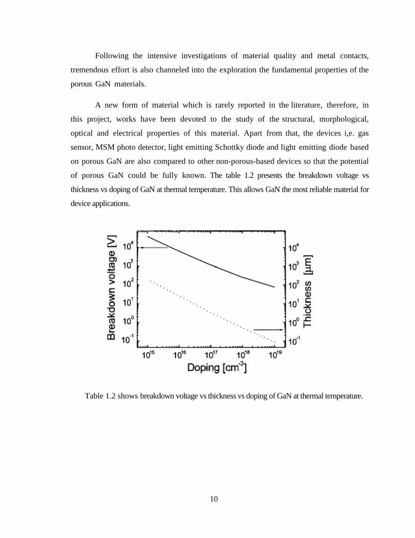
of porous GaN could be fully known. The table 1.2 presents the breakdown voltage vs
thickness vs doping of GaN at thermal temperature. This allows GaN the most reliable material for
device applications.
Table 1.2 shows breakdown voltage vs thickness vs doping of GaN at thermal temperature.
10
CHAPTER 2
GaN MATERIAL
2.1 INTRODUCTION
In this chapter, a brief overview of GaN technology is presented. The review
mainly focuses on the nitride semiconductors growth techniques, factors influencing the
GaN crystalline quality, metal-GaN contact technology and the development of the
porous GaN.
2.2 NITRIDE EPITAXIAL GROWTH TECHNIQUES
Tremendous efforts have been applied to the epitaxial growth of III-V nitride
materials. Most of the works so far can be divided into three categories: hydride vapor
phase epitaxial (HVPE), metal organic chemical vapor deposition (MOCVD), and
molecular beam epitaxial (MBE) methods.
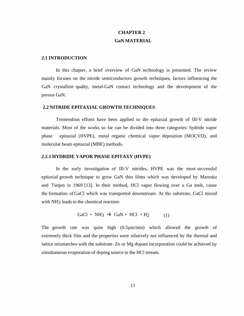
2.2.1 HYDRIDE VAPOR PHASE EPITAXY (HVPE)
In the early investigation of III-V nitrides, HVPE was the most successful
epitaxial growth technique to grow GaN thin films which was developed by Maruska
and Tietjen in 1969 [13]. In their method, HCl vapor flowing over a Ga melt, cause
the formation of GaCl which was transported downstream. At the substrate, GaCl mixed
with NH3 leads to the chemical reaction:
GaCl + NH3 GaN + HCl + H2 (1)
The growth rate was quite high (0.5μm/min) which allowed the growth of
extremely thick film and the properties were relatively not influenced by the thermal and
lattice mismatches with the substrate. Zn or Mg dopant incorporation could be achieved by
simultaneous evaporation of doping source in the HCl stream.
11
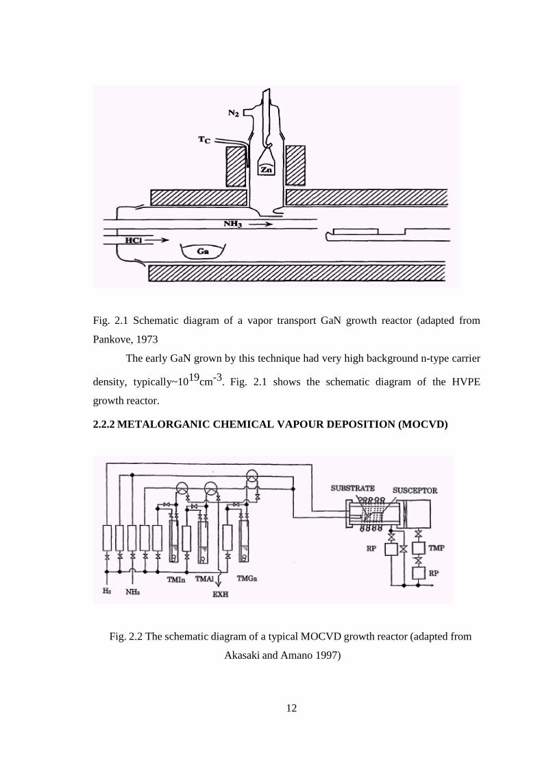
Fig. 2.1 Schematic diagram of a vapor transport GaN growth reactor (adapted from
Pankove, 1973
The early GaN grown by this technique had very high background n-type carrier
density, typically~1019cm-3. Fig. 2.1 shows the schematic diagram of the HVPE
growth reactor.
2.2.2 METALORGANIC CHEMICAL VAPOUR DEPOSITION (MOCVD)
Fig. 2.2 The schematic diagram of a typical MOCVD growth reactor (adapted from
Akasaki and Amano 1997)
12
Presently, MOCVD is the most successful and widely used technique for growing
nitride mater ia ls . It involves the transport of vapors of metal organic compound in a
carrier gas with thermal decomposition at or near the substrate. Fig.2.2 depicts the
schematic diagram of a typical MOCVD.
The general popularity of the MOCVD arises in part from its scalability to
production volumes of high quality multilayer hetero structures. However, the high
growth temperatures, necessary for efficient decomposition of the precursors, may
influence the quality of the grown hetero structures through thermal diffusion, with
large thermal expansion differentials introducing additional dislocation. Therefore,
many attempts have been made to reduce the MOCVD growth temperature by
providing additional, non-thermal, decomposition routes [ 1 3 ] . Many improved
versions have been developed since the introduction of this growth technique.
2.2.2.1 ATMOSPHERIC PRESSURE MOCVD
In conventional atmospheric pressure MOCVD reactor, III precursors used for the
growth of nitride materials come from metal-organic source i,e trimethylgallium
(TMGa/TMG) trimethylaluminum (TMAl/TMA), or trimethylindium (TMIn/TMI).
In the case of GaN growth, TMGa reacts with nitrogen in the form of NH3 which
requires high temperatures (typically 1000°C) to become reactive, and need to be
abundant, so that the III/V ratio is very small. This causes technical difficulties in flow
rate control, mixing and reactant flows over substrate [13]. In view of technical
difficulties, Nakamura designed a two-flow MOCVD reactor specifically for nitride
growth which has been highly successful. In this reactor, the main flow carries the
reactant gas parallel to the substrate. The second sub flow perpendicular to the
substrate forces, on the other hand a deviation of the reactant gas toward the
substrate, and suppress thermal convention effects. A rotating subsector was used to
enhance uniformity of the deposited films. The key aspect of this design is a downward
sub flow of H2 and N2 which has been claimed to improve the interaction of the
reactant gasses with the substrate. Fig. 2.3 shows the schematic diagram of the reactor.
13
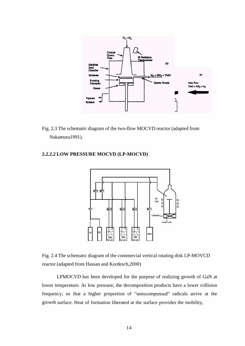
Fig. 2.3 The schematic diagram of the two-flow MOCVD reactor (adapted from
Nakamura1991).
2.2.2.2 LOW PRESSURE MOCVD (LP-MOCVD)
Fig. 2.4 The schematic diagram of the commercial vertical rotating disk LP-MOVCD
reactor (adapted from Hassan and Kordesch,2000)
LPMOCVD has been developed for the purpose of realizing growth of GaN at
lower temperature. At low pressure, the decomposition products have a lower collision
frequency, so that a higher proportion of “unrecompensed” radicals arrive at the
growth surface. Heat of formation liberated at the surface provides the mobility,
14
Necessary for the adsorbates to diffuse to nucleation sites with a reduced
requirement for kinetic energy to be provided by a hot substrate, making growth
possible. Fig. 2.4 shows the commercial vertical rotating disk LP-MOCVD reactor.
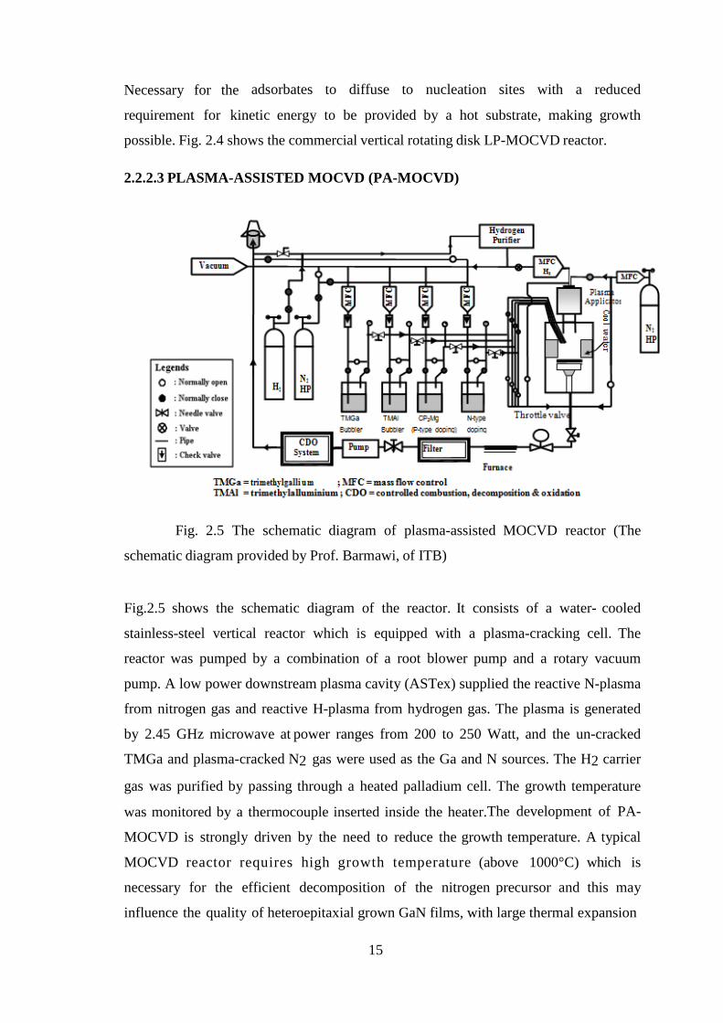
2.2.2.3 PLASMA-ASSISTED MOCVD (PA-MOCVD)
Fig. 2.5 The schematic diagram of plasma-assisted MOCVD reactor (The
schematic diagram provided by Prof. Barmawi, of ITB)
Fig.2.5 shows the schematic diagram of the reactor. It consists of a water- cooled
stainless-steel vertical reactor which is equipped with a plasma-cracking cell. The
reactor was pumped by a combination of a root blower pump and a rotary vacuum
pump. A low power downstream plasma cavity (ASTex) supplied the reactive N-plasma
from nitrogen gas and reactive H-plasma from hydrogen gas. The plasma is generated
by 2.45 GHz microwave at power ranges from 200 to 250 Watt, and the un-cracked
TMGa and plasma-cracked N2 gas were used as the Ga and N sources. The H2 carrier
gas was purified by passing through a heated palladium cell. The growth temperature
was monitored by a thermocouple inserted inside the heater.The development of PA-
MOCVD is strongly driven by the need to reduce the growth temperature. A typical
MOCVD reactor requires high growth temperature (above 1000°C) which is
necessary for the efficient decomposition of the nitrogen precursor and this may
influence the quality of heteroepitaxial grown GaN films, with large thermal expansion
15
differentials, thus introducing high densities of structural defects.
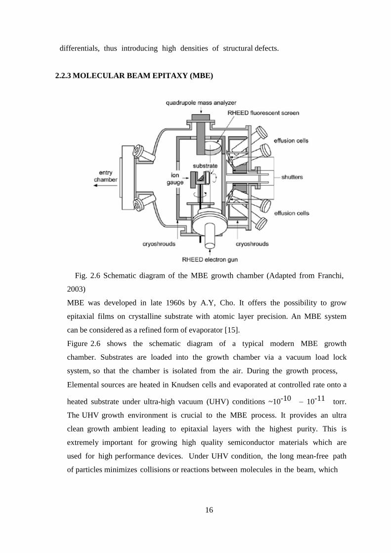
2.2.3 MOLECULAR BEAM EPITAXY (MBE)
Fig. 2.6 Schematic diagram of the MBE growth chamber (Adapted from Franchi,
2003)
MBE was developed in late 1960s by A.Y, Cho. It offers the possibility to grow
epitaxial films on crystalline substrate with atomic layer precision. An MBE system
can be considered as a refined form of evaporator [15].
Figure 2.6 shows the schematic diagram of a typical modern MBE growth
chamber. Substrates are loaded into the growth chamber via a vacuum load lock
system, so that the chamber is isolated from the air. During the growth process,
Elemental sources are heated in Knudsen cells and evaporated at controlled rate onto a
heated substrate under ultra-high vacuum (UHV) conditions ~10-10 – 10-11 torr.
The UHV growth environment is crucial to the MBE process. It provides an ultra
clean growth ambient leading to epitaxial layers with the highest purity. This is
extremely important for growing high quality semiconductor materials which are
used for high performance devices. Under UHV condition, the long mean-free path
of particles minimizes collisions or reactions between molecules in the beam, which
16
results is a line sight growth reaction at the surface. Since MBE is a UHV-based
technique, it has the advantage of being compatible with wide range of surface analysis
techniques. Mass spectrometer for residual gas analysis (RGA) and reflection high
energy electron diffraction (RHEED) are two important in situ analysis tools which
are commonly incorporated in the MBE system to monitor the growth rates and
epitaxial film quality during growth process [15].
GaN film grown by MBE usually carried out at relatively low temperatures of
650 to 800°C with typical growth rate of one to three monolayers per second,
approximately 0.3 to 1 µm/hr. On the other hand, molecular nitrogen is stable and inert
gas which has a strong N-N bond and does not chemisorb on a GaN surface for
temperature below 950°C, Therefore atomic nitrogen or nitrogen molecules with
weaker bonds should be supplied. Radio frequency (RF) or electron cyclotron
resonance (ECR) plasma sources are commonly employed to activate the nitrogen
species [15].
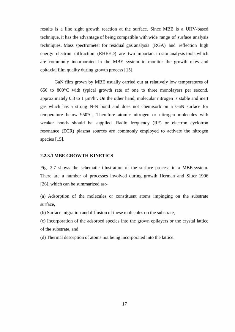
2.2.3.1 MBE GROWTH KINETICS
Fig. 2.7 shows the schematic illustration of the surface process in a MBE system.
There are a number of processes involved during growth Herman and Sitter 1996
[26], which can be summarized as:-
(a) Adsorption of the molecules or constituent atoms impinging on the substrate
surface,
(b) Surface migration and diffusion of these molecules on the substrate,
(c) Incorporation of the adsorbed species into the grown epilayers or the crystal lattice
of the substrate, and
(d) Thermal desorption of atoms not being incorporated into the lattice.
17
Fig 2.7 Schematic illustration of the surface processes during growth in a MBE system
(Adopted from Herman and Sitter 1996)
2.2.3.2 THE STRENGTHS OF MBE
Semiconductor compounds fabricated by MBE offers a number of advantages
compared to other growth techniques, for instances, the opening or closing of
mechanical shutter, located in front of each furnace, allows turning a specific molecular
beam on or off instantaneously, resulting in abrupt interfaces in the order of one
monolayer. This unique capability provides precise composition and doping profiles,
extremely well-defined layer; enable the fabrication of device structures with critical
performance. In addition, the consumption of source materials is significantly reduced
as compared to MOCVD.
The growth of GaN films by MBE at reduced temperatures not only allow wider range
of substrates to be investigated but also reduce the structural defects due to large
thermal expansion differentials. Moreover hydrogen-free environment also provides
the growth of p-type Mg-doped GaN without the need for post-growth
processing [19].
18
2.3 FACTORS INFLUENCING GAN CRYSTALLINE QUALITY
Many fundamental questions about the III-V nitrides growth are still being
raised. One of the major problems rests with the absence of well-suited substrates,
since GaN single crystals of sufficiently large dimensions are not yet available,
therefore GaN film has to be grown hetero-epitaxially on foreign substrates, this leads to
the generation of high density of structural defects.
However, the employment of low temperature buffer layer coupled with the
advancement of epitaxial growth techniques allow great enhancement in the
crystalline quality and subsequently the reduction of the high background electron
density in GaN, these lead to a tremendous improvement of carrier mobility and
eventually the performance of GaN-based devices.
2.3.1 SUBSTRATES
One of the major difficulties which hinder the GaN research is the lack of a
substrate material that is lattice matched and thermally compatible with GaN. High
dislocation densities arise in GaN epi layers due to the large mismatch between film
and substrate, contributing to the low mobility and high residual carrier density. In fact,
homoepitaxy is an ideal situation where it is possible to minimize problems associated
with difference in lattice, wetting as well as thermal expansion between substrate and
film. However, the equilibrium phase relationships between gallium, nitrogen and GaN
present formidable technological problems.
As a result, the bulk growth must resort to high temperatures of 1400oC -
1600°C and extremely high pressure of 12-15 kbar that Yield small size (few mm)
GaN [21].
19
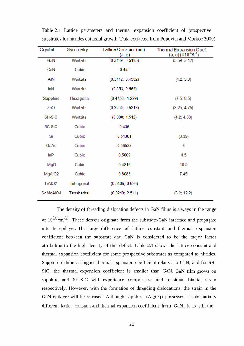
Table 2.1 Lattice parameters and thermal expansion coefficient of prospective
substrates for nitrides epitaxial growth (Data extracted from Popovici and Morkoc 2000)
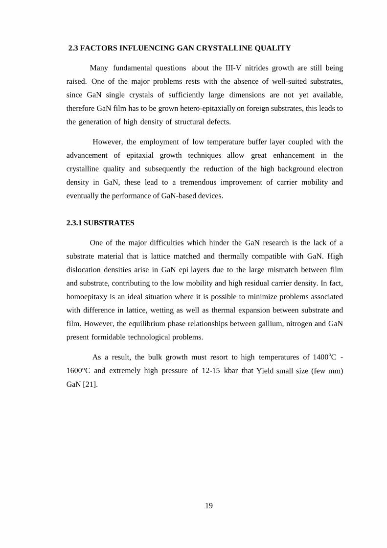
The density of threading dislocation defects in GaN films is always in the range
of 1010cm-2. These defects originate from the substrate/GaN interface and propagate
into the epilayer. The large difference of lattice constant and thermal expansion
coefficient between the substrate and GaN is considered to be the major factor
attributing to the high density of this defect. Table 2.1 shows the lattice constant and
thermal expansion coefficient for some prospective substrates as compared to nitrides.
Sapphire exhibits a higher thermal expansion coefficient relative to GaN, and for 6H-
SiC, the thermal expansion coefficient is smaller than GaN. GaN film grows on
sapphire and 6H-SiC will experience compressive and tensional biaxial strain
respectively. However, with the formation of threading dislocations, the strain in the
GaN epilayer will be released. Although sapphire (Al2O3) possesses a substantially
different lattice constant and thermal expansion coefficient from GaN, it is still the
20
most commonly used substrate for GaN growth because of its wide availability,
hexagonal symmetry, and ease of handling and pre-growth cleaning. Sapphire is also
stable at high temperature (~1000 °C), which is normally required for GaN film
grown by metal organic chemical vapor deposition (MOCVD) method. On the other
hand, sapphire is electrically insulating, therefore, all electrical contacts have to be
formed on the front side of the device, reducing the area available for devices and
complicating the device fabrication [22].
Si is another potential substrate due to the low price, high quality and wide
availability as well as easy integration with the current silicon technology. Both Si
(110) and (111) are employed for Wurtzitic GaN growth. However, GaN grown on Si
(001) is predominantly cubic (Popovici and Morkoc 2000).
Table 2.2 Lattice mismatch between GaN and the most commonly used substrates
adapted from (Popovici and Morkoc 2000).
6H-SiC exhibits a closer lattice constant and thermal expansion coefficient to GaN,
however, this substrate is very expensive. GaAs has been used as substrate despite its
poor compatibility. This is mainly due to its widely availability and familiarity of the
researchers. Other uncommon substrates such as MgO, ZnO, MgAl2O4, also have been
used as substrate, however, there are little technical information available in the
literature, therefore, the use of these substrates need to be further developed and
explored.
Lattice mismatch between GaN and the most commonly used substrates is
summarized in Table 2.2.
21
2.3.2 BUFFER LAYER
Since GaN single crystals with practically large dimensions are not
yet available, single crystalline film has to be grown heteroepitaxially on substrates
which are normally not lattice matched and thermally compatible. Therefore
heteroepitaxial growth is accompanied with high density of structural defects such as
stacking faults, threading dislocation, as well as vacancies and impurities [Ref 30],
which form shallow and deep levels inside the band gap and eventually degrade the
optical and electrical properties of the films. The major problem in obtaining high
quality heteroepitaxial grown GaN film is mainly due to the formation of defects in
the nucleation layer which is attributed to the inhomogeneous wetting of the substrate.
Therefore direct deposition of GaN on substrates would result in poor crystalline
quality of the film. The introduction of low temperature buffer layer is one of the
promising approaches that can reduce the structural defect significantly. AlN is
commonly used as a buffer for GaN grown on sapphire. Buffers are amorphous-like
structure with small crystallites which are normally deposited at about 600°C with
layer thickness between 50 – 100 nm prior to the growth of GaN film. The initial
growth stage is very important in obtaining heteroepitaxy and eventually a good
quality of the film. The epitaxial growth can be a two-dimensional (2-D) layer-by-layer
mode, a three-dimensional (3-D) island mode, or a mixed mode: layer-by-layer plus
islands. The first mode would result in the smooth surface, while the last two modes
give rough surface and lead to low quality of epitaxial layers. The mode of growth is
governed by many factors. For instances, the interfacial energy of the solid and vapor
phases, as well as the vapor phase and substrate. This in turn depends on the growth
temperature, the bond strength and bond lengths of the substrate and the overgrowth
atoms, the rate of species impingement, surface migration rates of reactants,
super saturation of the gas phase, and the size of critical nuclei adapted from Popovici
and Morkoc 2000 [31].
There has been reported that GaN films grown with AlN buffer layer have led to
two orders of magnitude reduction in background electron while increasing the carrier
mobility by a factor of 10, and the near band gap photoluminescence was two orders of
magnitude more intense, moreover the x-ray diffraction peak width was four times
smaller. The buffer layer reduces the effect of strain, dislocations and cracking defect
in the GaN films on large lattice and thermally-mismatched substrates
22
significantly [32]. The buffer layer not only relaxes the strain in the heteroepitaxial
growth but partly blocks the detrimental effect of the substrate, such as the
crystallographic orientation of the substrate [ 3 2 ] .
The buffer layer is also thought to play an important role in supplying
nucleation centres which have the same orientation as the substrate and promoting the
lateral growth of the film due to the decrease in interfacial free energy between
the film and the substrate.
2.4 OVERVIEW OF METAL-GaN CONTACT TECHNOLOGY
2.4.1 OHMIC CONTACT ON GaN
As the GaN device technology advances, more stringent requirements are
needed for the fabrication of metal contacts with very low resistance, good thermal
stability, and flat surface morphology. It is widely known that parasitic resistances, in
the form of contact resistance, significantly affect the overall performance of the
electronic and optical devices. The large voltage drop across the semiconductor/metal
interface at the ohmic contacts will seriously lead to the loss of device performance and
reliability, for instance, in LEDs the power loss at the contacts will reduce the wall-
plug efficiency and increase the junction temperature. This potentially degrades the
operating lifetime. Therefore, high quality, thermally stable contacts to GaN-based
materials are essential for the fabrication of reliable, efficient, high performance devices
and circuits.
A wide variety of metallization for ohmic contacts on n-GaN have been
intensively investigated. From the literature, contact resistances below 10-5 Ω-cm2
can be achieved routinely and low contact resistance as low as 10-8Ω-cm2 has been
reported [ 33] , which is good enough for the optical and electronic devices.
However, for p-type GaN, the typical values of contact resistance are higher than 10-4
Ω-cm2. Low-resistance ohmic contact to p-GaN is difficult to obtain due to the
difficulty in achieving high carrier concentration (~1018 cm-3 and above), and the
absence of suitable metals with high work function, larger than band gap and
electron affinity of GaN (7.5 eV) [33] . These two obstacles have impeded the
fabrication of highly efficient blue LEDs and LDs.
23
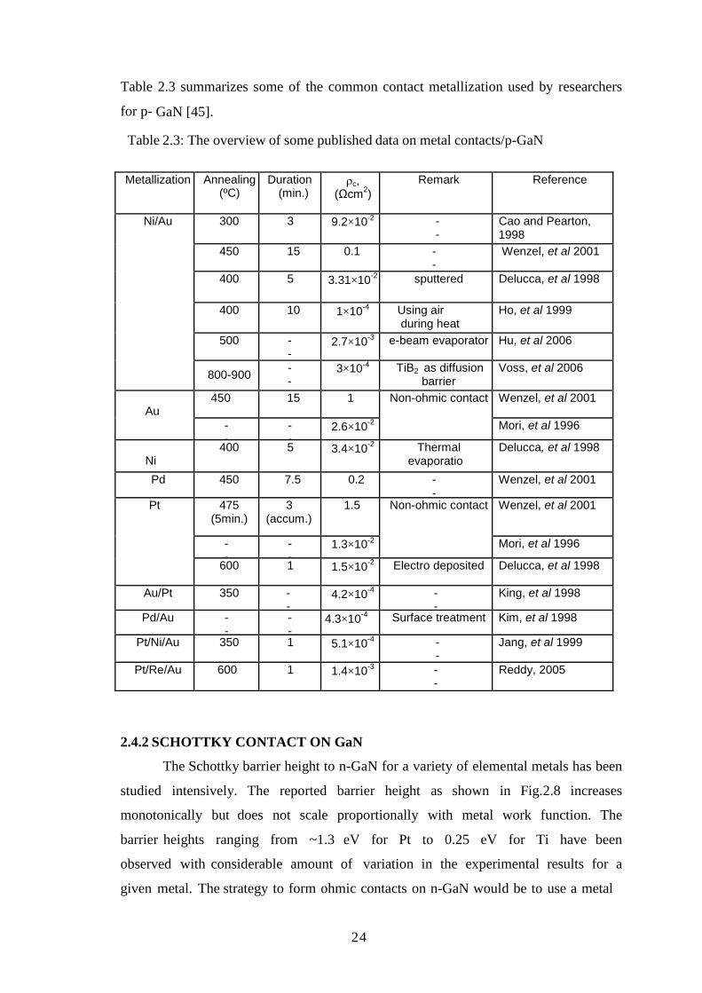
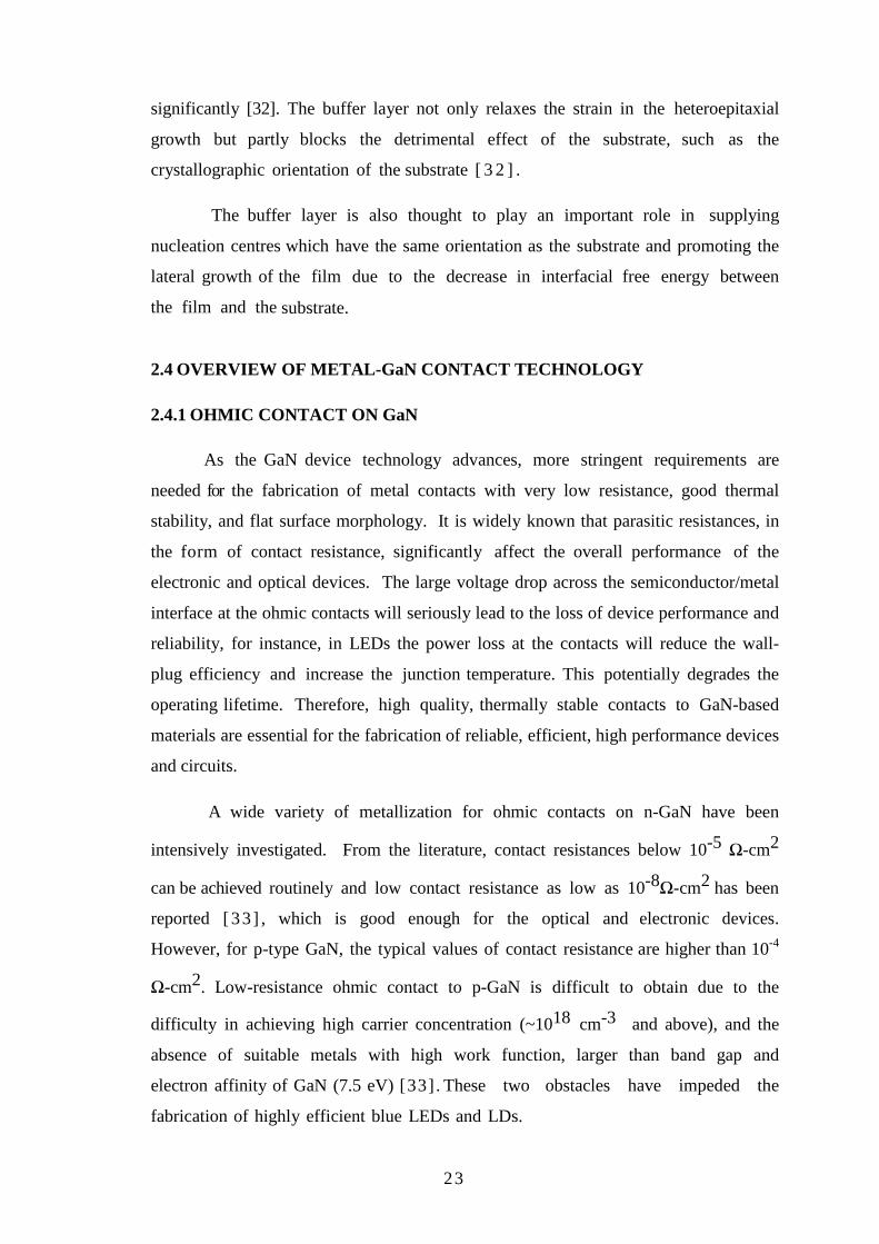
Table 2.3 summarizes some of the common contact metallization used by researchers
for p- GaN [45].
Table 2.3: The overview of some published data on metal contacts/p-GaN
Metallization Annealing
(ºC) Duration
(min.) ρc,
(Ωcm2)
Remark Reference
Ni/Au 300 3 9.2×10⁻² --
Cao and Pearton, 1998
450 15 0.1 --
Wenzel, et al 2001
400 5 3.31×10⁻² sputtered Delucca, et al 1998
400 10 1×10⁻⁴ Using air
during heat treatment
Ho, et al 1999
500 --
2.7×10⁻³ e-beam evaporator Hu, et al 2006
800-900 --
3×10-4 TiB2 as diffusion barrier
Voss, et al 2006
Au
450 15 1 Non-ohmic contact Wenzel, et al 2001
--
--
2.6×10⁻² Mori, et al 1996
Ni
400 5 3.4×10⁻² Thermal
evaporation
Delucca, et al 1998
Pd 450 7.5 0.2 --
Wenzel, et al 2001
Pt 475 (5min.)
3 (accum.)
1.5 Non-ohmic contact Wenzel, et al 2001
--
--
1.3×10⁻² Mori, et al 1996
600 1 1.5×10⁻² Electro deposited Delucca, et al 1998
Au/Pt 350 --
4.2×10⁻⁴ -
- King, et al 1998
Pd/Au --
--
4.3×10⁻⁴ Surface treatment Kim, et al 1998
Pt/Ni/Au 350 1 5.1×10⁻⁴ -
- Jang, et al 1999
Pt/Re/Au 600 1 1.4×10⁻³ -
- Reddy, 2005
2.4.2 SCHOTTKY CONTACT ON GaN
The Schottky barrier height to n-GaN for a variety of elemental metals has been
studied intensively. The reported barrier height as shown in Fig.2.8 increases
monotonically but does not scale proportionally with metal work function. The
barrier heights ranging from ~1.3 eV for Pt to 0.25 eV for Ti have been
observed with considerable amount of variation in the experimental results for a
given metal. The strategy to form ohmic contacts on n-GaN would be to use a metal
24
with a small work function such as Ti and Al, on the other hand, to use a metal with
large work function such as Pt to form Schottky barriers on n-GaN. A survey of the
literature shows that this principle is generally followed in fabricating contacts on n-
GaN.
Fig.2.8. Reported barrier heights of metals to n-GaN as a function of their work
function adapted from Liu and Lau, 1998 [30].
Small measured values of the Richardson constant, A as compared to
theoretical value, and the ideality factor, n which is significantly greater than unity are
the commonly observed non-ideal behavior of GaN Schottky diodes which can be
caused by several factors. For instances, surface defects which lead to in homogeneities
in the transport current, or several transport mechanisms operating at the same time or
both. GaN grown by various techniques is known to produce high density of
structural defects, these defects are likely to be the primary reason for non- ideal I-V
curves and small experimental values of A** [Ref 33]. Another crucial factor
affecting the properties of Schottky contacts on GaN and metal contacts is the
metal- semiconductor (MS) reactions. MS reactions are known to depend strongly
on the interface and interfacial reaction between contact metal and semiconductor
frequently.
25
CHAPTER 3
SCHOTTKY DIODE
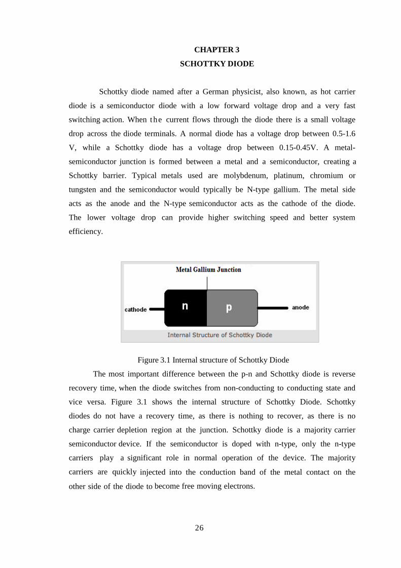
Schottky diode named after a German physicist, also known, as hot carrier
diode is a semiconductor diode with a low forward voltage drop and a very fast
switching action. When the current flows through the diode there is a small voltage
drop across the diode terminals. A normal diode has a voltage drop between 0.5-1.6
V, while a Schottky diode has a voltage drop between 0.15-0.45V. A metal-
semiconductor junction is formed between a metal and a semiconductor, creating a
Schottky barrier. Typical metals used are molybdenum, platinum, chromium or
tungsten and the semiconductor would typically be N-type gallium. The metal side
acts as the anode and the N-type semiconductor acts as the cathode of the diode.
The lower voltage drop can provide higher switching speed and better system
efficiency.
Figure 3.1 Internal structure of Schottky Diode
The most important difference between the p-n and Schottky diode is reverse
recovery time, when the diode switches from non-conducting to conducting state and
vice versa. Figure 3.1 shows the internal structure of Schottky Diode. Schottky
diodes do not have a recovery time, as there is nothing to recover, as there is no
charge carrier depletion region at the junction. Schottky diode is a majority carrier
semiconductor device. If the semiconductor is doped with n-type, only the n-type
carriers play a significant role in normal operation of the device. The majority
carriers are quickly injected into the conduction band of the metal contact on the
other side of the diode to become free moving electrons.
26
Therefore no slow, random recombination of n-type and p-type carriers is
involved, so that this diode can cease conduction faster than an ordinary p-n
rectifier diode.
This property allows a smaller device area, which also makes a faster
transition and hence Schottky diodes are used in switch-mode power converters. The
circuit can operate at frequencies in the range 200 KHz to 2 MHz. Small- area Schottky
diodes are the heart of RF detectors and mixers, which can operate up to 50 GHz.
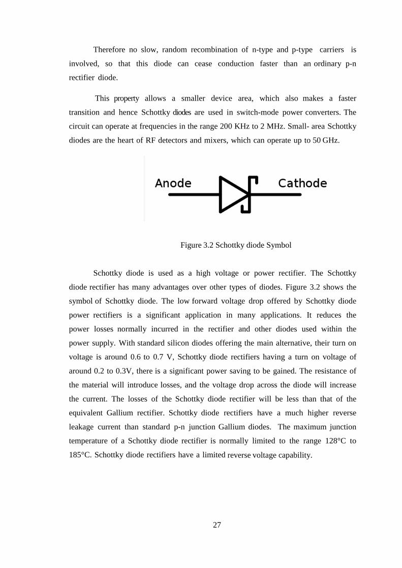
Figure 3.2 Schottky diode Symbol
Schottky diode is used as a high voltage or power rectifier. The Schottky
diode rectifier has many advantages over other types of diodes. Figure 3.2 shows the
symbol of Schottky diode. The low forward voltage drop offered by Schottky diode
power rectifiers is a significant application in many applications. It reduces the
power losses normally incurred in the rectifier and other diodes used within the
power supply. With standard silicon diodes offering the main alternative, their turn on
voltage is around 0.6 to 0.7 V, Schottky diode rectifiers having a turn on voltage of
around 0.2 to 0.3V, there is a significant power saving to be gained. The resistance of
the material will introduce losses, and the voltage drop across the diode will increase
the current. The losses of the Schottky diode rectifier will be less than that of the
equivalent Gallium rectifier. Schottky diode rectifiers have a much higher reverse
leakage current than standard p-n junction Gallium diodes. The maximum junction
temperature of a Schottky diode rectifier is normally limited to the range 128°C to
185°C. Schottky diode rectifiers have a limited reverse voltage capability.
27
3.1 GALLIUM NITRIDE SCHOTTKY DIODE
Schottky diodes constructed from Gallium Nitride have a much lower reverse
leakage current as compared to a Gallium Schottky diode. As of 2011, these diodes
are available in variants up to 1700 V. Gallium Nitride has a high thermal
conductivity and temperature has a little influence on its switching and thermal
characteristics. With special packaging, it is possible to have operating temperatures
of over 500 K, which allows passive radiation cooling in aerospace applications.
These are wide energy gap devices, with high-saturated electron velocity and high
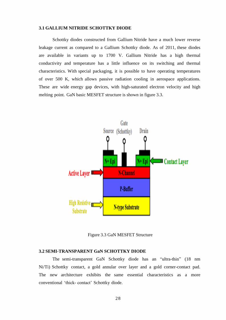
melting point. GaN basic MESFET structure is shown in figure 3.3.
Figure 3.3 GaN MESFET Structure
3.2 SEMI-TRANSPARENT GaN SCHOTTKY DIODE
The semi-transparent GaN Schottky diode has an “ultra-thin” (18 nm
Ni/Ti) Schottky contact, a gold annular over layer and a gold corner-contact pad.
The new architecture exhibits the same essential characteristics as a more
conventional ‘thick- contact’ Schottky diode.
28
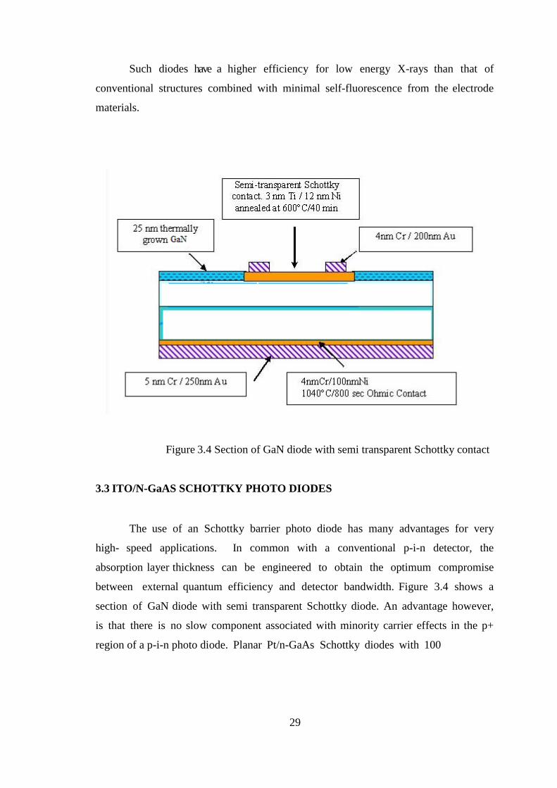
Such diodes have a higher efficiency for low energy X-rays than that of
conventional structures combined with minimal self-fluorescence from the electrode
materials.
Figure 3.4 Section of GaN diode with semi transparent Schottky contact
3.3 ITO/N-GaAS SCHOTTKY PHOTO DIODES
The use of an Schottky barrier photo diode has many advantages for very
high- speed applications. In common with a conventional p-i-n detector, the
absorption layer thickness can be engineered to obtain the optimum compromise
between external quantum efficiency and detector bandwidth. Figure 3.4 shows a
section of GaN diode with semi transparent Schottky diode. An advantage however,
is that there is no slow component associated with minority carrier effects in the p+
region of a p-i-n photo diode. Planar Pt/n-GaAs Schottky diodes with 100
29
GHz bandwidth have been reported by Wang et al ; the metal thickness was only
100Å to allow for optocoupling. An inherent disadvantage of the Schottky photo
diode, however, is the high series resistance and low efficiencies arising from the
semi-transparent metal layer. This is apparent in the relatively low quantum efficiency
of 19% and high series resistance of190Ω obtained by Emeis et al in their p-InGaAs
Schottky diodes (for operation at 1.3µm wavelength) with 50Å Ni semi-transparent
metal contact.Using a practically transparent and highly conductive layer of
Indium Tin Oxide (ITO) to form the metal/semiconductor junction solves both
these problems.
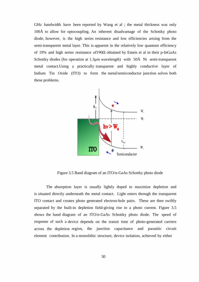
Figure 3.5 Band diagram of an ITO/n-GaAs Schottky photo diode
The absorption layer is usually lightly doped to maximize depletion and
is situated directly underneath the metal contact. Light enters through the transparent
ITO contact and creates photo generated electron-hole pairs. These are then swiftly
separated by the built-in depletion field-giving rise to a photo current. Figure 3.5
shows the band diagram of an ITO/n-GaAs Schottky photo diode. The speed of
response of such a device depends on the transit time of photo-generated carriers
across the depletion region, the junction capacitance and parasitic circuit
element contribution. In a monolithic structure, device isolation, achieved by either
30
proton bombardment or mesa etches or a combination of both reduces these parasitics.
Furthermore, a planar structure is suitable for monolithic integration with other
circuit elements such as HBTs or HEMTs.
3.4 DIODE FABRICATION
3.4.1 GROWN JUNCTION DIODE
Diodes of this type are formed during the crystal pulling process. P and N-
type impurities can be alternately added to the molten semiconductor material in the
crucible, which results in a P-N junction. The larger area device then can be cut into
a large number of smaller-area semiconductor diodes after slicing. The larger area also
introduces more capacitive effects, which are undesirable. Such diodes are used for
low frequencies.
3.4.2 ALLOY TYPED OR FUSED JUNCTION DIODE
Placing a P-type impurity into the surface of an N-type crystal and heating
the two until liquefaction occurs form an Alloy type or a Fused Junction diode. An alloy
that will result on cooling will give a P-N junction at the boundary of the alloy
substrate. Alloy type diodes have a high current rating and large PIV (Peak Inverse
voltage) rating. The junction capacitance is also large, due to the large junction area.
The figure 3.6 shows the alloy type or fused junction diode.
Figure 3.6 Alloy Type or Fused Junction Diode
31
3.4.3 DIFFUSED JUNCTION DIODE
Diffusion is a process by which a heavy concentration of particles diffuses into
a surrounding region of lower concentration. The main difference between the
diffusion and alloy process is that the liquefaction is not reached in the diffusion
process. In the diffusion process heat is applied only to increase the activity of
elements involved. The process of solid diffusion starts with the formation of layer of
an acceptor impurity on an N-type substrate and heating the two until the impurity
diffuses into the substrate to form the P-type layer. A large p-n junction is divided
into parts by cutting process. Metallic contacts are made for connecting anode and
cathode leads.
In the process of gaseous diffusion instead of layer formation of an acceptor
impurity, an N-type substrate is placed in a gaseous atmosphere of acceptor
impurities ad then heated. The impurity diffuses into the substrate to form P- type
layer on the N- type substrate. Diffusion process requires more time than the alloy
process but is relatively expensive, and can be very accurately controlled. The
diffusion technique leads to the simultaneous fabrication of many hundreds of diodes
on one small disc of semiconductor material and is most commonly used in the
manufacture of semiconductor diodes. Diffusion process is also used in the production
of transistors and ICs (Integrated Circuits). Figure 3.7 shows Diffused Junction Diode.
Figure 3.7 Diffusion Junction Diode
32
3.4.4 EPITAXIAL GROWTH OR PLANAR DIFFUSED DIODE
The term,“epitaxial is derived from the Latin terms epi meaning ‘upon’ and
taxis meaning ‘arrangement’. To construct an epitaxial grown diode, a very thin high
impurity layer of semiconductor material is grown on a heavily doped substrate of
the same material. This complete structure then forms the N-region on which P-region
is diffused. GaN layer is thermally grown on the top surface, photo-etched and then
aluminium contact is made to the P-region. A metallic layer at the bottom of the
substrate forms the cathode to which lead is attached. Epitaxial Growth is usually
employed in fabrication of IC chips. Figure 3.8 shows epitaxially grown or planar
diffused diode.
Figure 3.8 Epitaxially Grown or Planar diffused Diode
3.4.5 POINT CONTACT DIODE
Point contact diode consists of an N-type germanium or silicon wafer about 12.5mm
square by 0.5 mm thick, one face of which is soldered to a metal base by radio-
frequency heating and the other face has a phosphor bronze pressed against it. Because
of the small area of junction, point contact diode can be used to rectify only very small
currents. The shunting capacitance of the point contact diodes is very valuable in
equipment operating at super high frequencies (as high as 25,000 MHz). Figure 3.9
shows point contact diode.
33
Figure 3.9 Point Contact Diode
Table 3.1 showing the material properties of several semiconductors for fabrication of
the Schottky barrier diode [36].
MATERIAL
Eg (eV)
ɛr
K(w/k-
cm)
Ec
(V/cm)
Si 1.12 11.9 1.5 3x10⁵
GaAS 1.43 12.5 0.54 4x10⁵
InP 1.34 12.4 0.67 4.5x10⁵
4H-SiC 3.2 10.0 4 1.5x10⁶
6H-SiC 2.86 10.0 4 1.5x10⁶
GaN 3.4 9.5 1.3 3.5x10⁵
Diamond 5.6 5.5 20-30 5x10⁶
Table 3.1 shows the material properties of several semiconductors for
fabrication of the Schottky barrier diode.
34
CHAPTER 4
EXTRACTING THE PARAMETERS
4.1 BASIC THEORETICAL DERIVATIONS
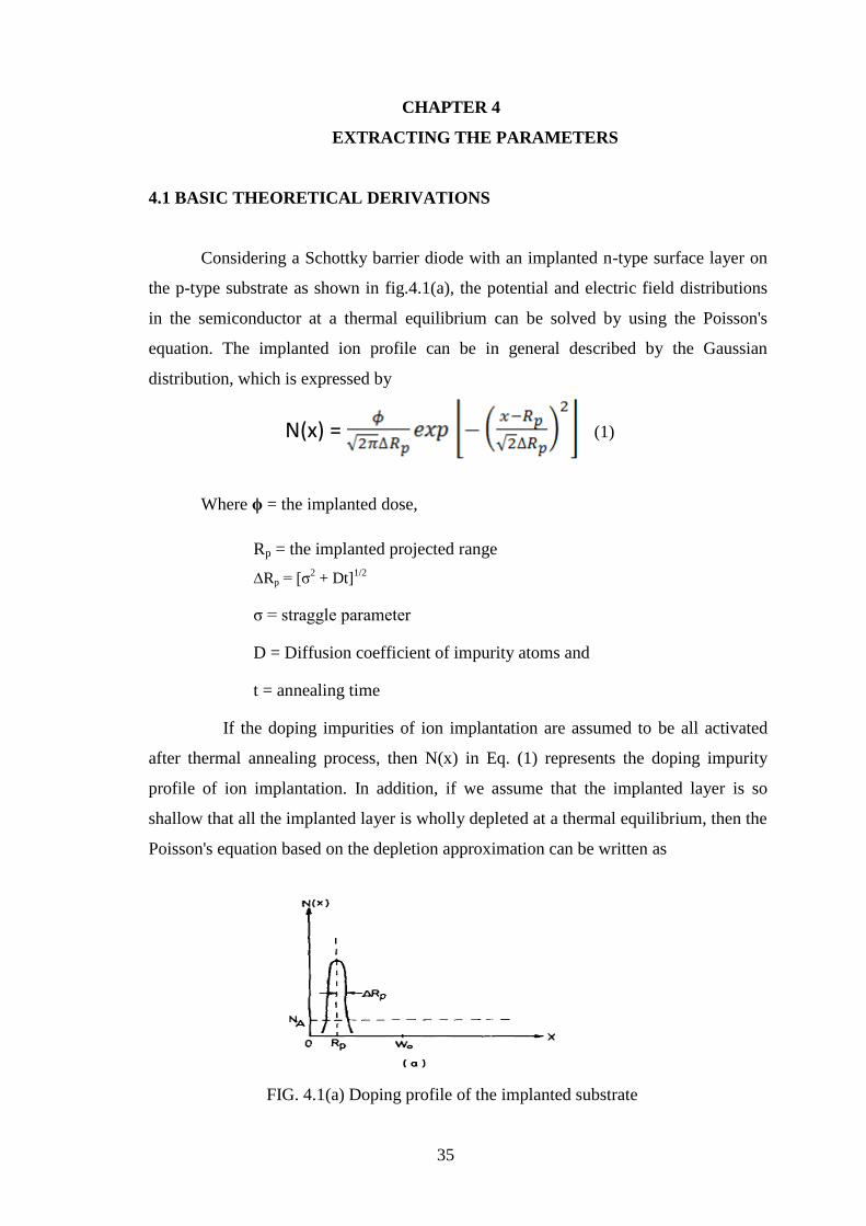
Considering a Schottky barrier diode with an implanted n-type surface layer on
the p-type substrate as shown in fig.4.1(a), the potential and electric field distributions
in the semiconductor at a thermal equilibrium can be solved by using the Poisson's
equation. The implanted ion profile can be in general described by the Gaussian
distribution, which is expressed by
N(x) = (1)
Where ϕ = the implanted dose,
Rp = the implanted projected range
∆Rp = [σ2 + Dt]
1/2
σ = straggle parameter
D = Diffusion coefficient of impurity atoms and
t = annealing time
If the doping impurities of ion implantation are assumed to be all activated
after thermal annealing process, then N(x) in Eq. (1) represents the doping impurity
profile of ion implantation. In addition, if we assume that the implanted layer is so
shallow that all the implanted layer is wholly depleted at a thermal equilibrium, then the
Poisson's equation based on the depletion approximation can be written as
FIG. 4.1(a) Doping profile of the implanted substrate
35
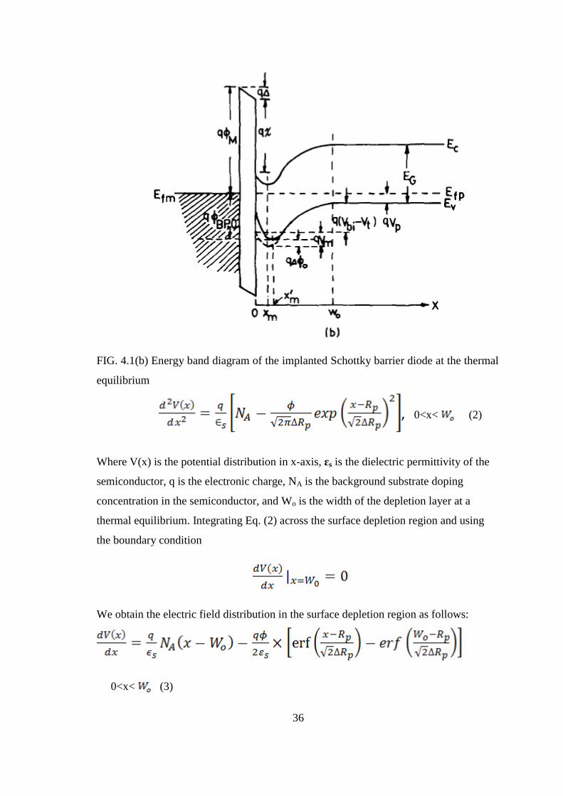
FIG. 4.1(b) Energy band diagram of the implanted Schottky barrier diode at the thermal
equilibrium
, 0<x< (2)
Where V(x) is the potential distribution in x-axis, ɛs is the dielectric permittivity of the
semiconductor, q is the electronic charge, NA is the background substrate doping
concentration in the semiconductor, and Wo is the width of the depletion layer at a
thermal equilibrium. Integrating Eq. (2) across the surface depletion region and using
the boundary condition
We obtain the electric field distribution in the surface depletion region as follows:
0<x< (3)
36
Where erf(y) is the error function with the argument y. Integrating Eq. (3) across the
surface depletion region and using the boundary conditions, V(x = 0) = 0 and V (x =
Wo) = - (Vbi – Vt), the potential distribution in the surface depletion region can be
expressed by
V(x) =
---- (4)
and the total depletion layer width Wo at a thermal equilibrium can be expressed by
------ (5)
With the surface-implanted n-layer in the p substrate, it is known that there is a
maximum potential point X m in the depletion region of the semiconductor as shown in
Fig.4.1(b).The expression for obtaining the maximum potential point can be easily
calculated by setting Eq. (3) to zero, i.e.,
The result is
(6)
And the maximum potential relative to the semiconductor at X=0 (metallurgical
function)
37
----- (7)
If the implanted layer is very thin, the effect of image force potential on the location and
magnitude of the maximum potential must be taken into consideration. In this case, the
previous zero potential reference at X = 0 must be shifted to the peak potential at X =
Xm' and Vm is the maximum relative potential then the total potential including the
image-force potential can be expressed by
(8)
Where V (x) is expressed by Eq. (4), Vm is expressed by Eq. (7), and the last term
represents the image-force potential with the dynamic permittivity Esd'. The location of
the maximum potential point with considering the image-force effects Xm’ can be
obtained by the boundary condition
This yields
----- (9)
Note that the first two terms in Eq. (7) are simply obtained by using Eq. (6) with x =
xm’.The image-force lowering in this case can be calculated by substituting X with Xm’
in Eq. (8), which is expressed by
(10)
From the energy band diagram shown in Fig. 4.l (b), the effective barrier height for
holes at the thermal equilibrium can be expressed by
(11)
38
Using Equations (4), (9), and (10), the effective barrier height for holes in equation 11
can be expressed by
------ (12)
Where Vp is the potential difference between the valence band edge and the Fermi level
in the neutral p substrate. From Eq. (12) it is clearly seen that Wo and Xm must be
calculated iteratively by using Equations. (5) and (9) if Vbi – Vt and the parameters of
the implanted profile are known.
4.2 INTERFACIAL LAYER MODEL FOR THE BARRIER HEIGHT
ENHANCEMENT
It is a known fact that the barrier height of a conventional Schottky barrier diode is
determined by the work function difference between the metal and the semiconductor,
the density of interface states, and the interfacial layer properties. Similarly, for a
Schottky barrier diode with surface ion implantation, an interfacial layer theory must be
developed in order to calculate the expression of the built-in voltage. The energy-band
diagram of a GaN Schottky diode with an interfacial layer is known. Assuming that the
semiconductor surface has acceptor-like surface states with density Dsa (states/cm2/eV),
and Dsa is a constant over the energy range from qϕo to the Fermi-level, then the charge
density in the interface state Qss is given by
(13)
The space-charge density in the surface depletion layer of the semiconductor at the
thermal equilibrium can be calculated by using Eq. (3). The result is
(14)
39
Where Wo is represented by Eq. (5) and erf(-A) = - erf(A ) has been used. According to
the energy-band diagram shown in Fig. 2, the potential energy across the interfacial
layer q∆ may be written as
(15)
Where EG the energy gap of the semiconductor, qX is is is the electron affinity of the
semiconductor, and qM is the work function of the metal. Using Gauss' law, the potential
across the interfacial layer may be related to the induced charge density at the metal
surface QM by
(16)
Where the thickness of the interfacial layer, ɛi is is the static permittivity of the
interfacial layer, and Qs is the fixed interface change density between the semiconductor
and the interfacial layer. Putting equations (13), (14), and (15) into Eq. (16), we obtain
------- (17)
(18)
(19)
For a practical Schottky barrier diode, the thickness of the interfacial layer is of the
atomic dimension, so the ()1/2 term in Eq. (17) may be neglected if NA is small. In this
case, the built-in voltage can be approximately written as
(20)
40
Where k = q C2/ ɛi is a characteristic parameter of the interfacial layer; Vbio is defined
as the built-in voltage without the implanted surface layer and at the thermal
equilibrium, which is expressed by
(21)
From Eq. (20), it is clearly seen that the implanted n layer on the p-type substrate will
increase the built-in voltage across the surface depletion region. Putting Equations (20)
and (21) into Eq. (12), the barrier height at the thermal equilibrium for a Schottky
barrier diode with surface n layer on the p type substrate can be expressed by
---------- (22)
If the interfacial layer properties of a Schottky barrier diode are assumed to be
unchanged after the insertion of the implanted layer, then the barrier height without the
implanted n layer can be written as
(23)
where ∆ϕoo is the image-force lowering without the doped surface layer, which can be
approximately expressed by
(24)
The barrier height enhancement in this case can be written as
41
------- (25)
Where Xm’ can be computed from Eq. (50) by using the iterative method in which W0 is
first solved by the following explicit expression:
------- ( 26)
The condition for with annealing is obtained by substituting [σ2 + Dt]1/2 for ∆Rp where σ
is the same straggle parameter typically for GaN (0.42 x 10⁻⁶
) and D is the diffusion
coefficient and t is the annealing time.
It is clearly seen that if the implanted parameters (Rp, ∆Rp, ϕ) are known, W0 and Xm’
can be iteratively computed for the given surface parameter K and ϕBPO then Vm(Xm’)
and the barrier height enhancement can be obtained.
42
CHAPTER 5
NUMERICAL RESULTS & EXPERIMENTAL COMPARISIONS
The computer calculations for the barrier height enhancement of the Schottky barrier
diode were done by a numerically iterative method in which the roots of the polynomial
and transcendental equations were computed by using the half-interval algorithm for the
condition of convergence. Typical plots for the peak position X’m of the potential
barrier as functions of the implanted ion dose and different projected range, where the
straggle parameter takes the practical value of the projected range and the surface
characteristics parameter k is assumed to be zero for the ideal case. When the
implantation depth is very shallow, the potential contributed from the implanted ion
dose is negligible, and then the peak potential positions are determined by the built-in
potential of no implantation. However, when the implantation is slightly deeper, the
peak position of the maximum potential is always located in the doped layer, and higher
dose will shift the peak position from the contact surface to the metallurgical junction of
the n+-p junction. The analytical model also includes the post annealing effect, which is
extremely important to accurately develop the physics model.
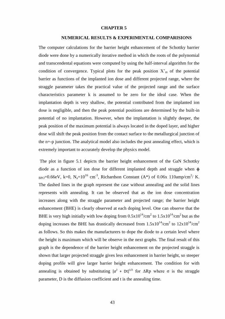
The plot in figure 5.1 depicts the barrier height enhancement of the GaN Schottky
diode as a function of ion dose for different implanted depth and straggle when ϕ
BPO=0.66eV, k=0, Na=1016
cm-3
, Richardson Constant (A*) of 0.06x 110amp/cm2/ K.
The dashed lines in the graph represent the case without annealing and the solid lines
represents with annealing. It can be observed that as the ion dose concentration
increases along with the straggle parameter and projected range; the barrier height
enhancement (BHE) is clearly observed at each doping level. One can observe that the
BHE is very high initially with low doping from 0.5x10¹⁴
/cm2 to 1.5x10
14/cm
2 but as the
doping increases the BHE has drastically decreased from 1.5x10¹⁴
/cm2 to 12x10
14/cm
2
as follows. So this makes the manufacturers to dope the diode to a certain level where
the height is maximum which will be observe in the next graphs. The final result of this
graph is the dependence of the barrier height enhancement on the projected straggle is
shown that larger projected straggle gives less enhancement in barrier height, so steeper
doping profile will give larger barrier height enhancement. The condition for with
annealing is obtained by substituting [σ2 + Dt]1/2 for ∆Rp where σ is the straggle
parameter, D is the diffusion coefficient and t is the annealing time.
43
At all the points the consideration of with annealing gives better accurate device
modeling results than that of without-annealing. This graph was plotted using the
equation 26 and Wo has been calculated by using iterative method and the value is later
substituted.
Fig. 5.1 A plot of the Barrier Height Enhancement (eV) of the GaN Schottky diode as a
function of ion dose (cm-2
) for different implanted depth and straggle when ϕ
BPO=0.66eV, k=0, Na=1016
cm-3
, Richardson Constant (A*) of 0.06x 110amp/cm2/ K.
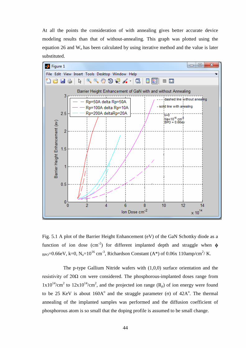
The p-type Gallium Nitride wafers with (1,0,0) surface orientation and the
resistivity of 20Ω cm were considered. The phosphorous-implanted doses range from
1x10¹⁴
/cm2 to 12x10
14/cm
2, and the projected ion range (Rp) of ion energy were found
to be 25 KeV is about 160Ao and the straggle parameter (σ) of 42A
o. The thermal
annealing of the implanted samples was performed and the diffusion coefficient of
phosphorous atom is so small that the doping profile is assumed to be small change.
44
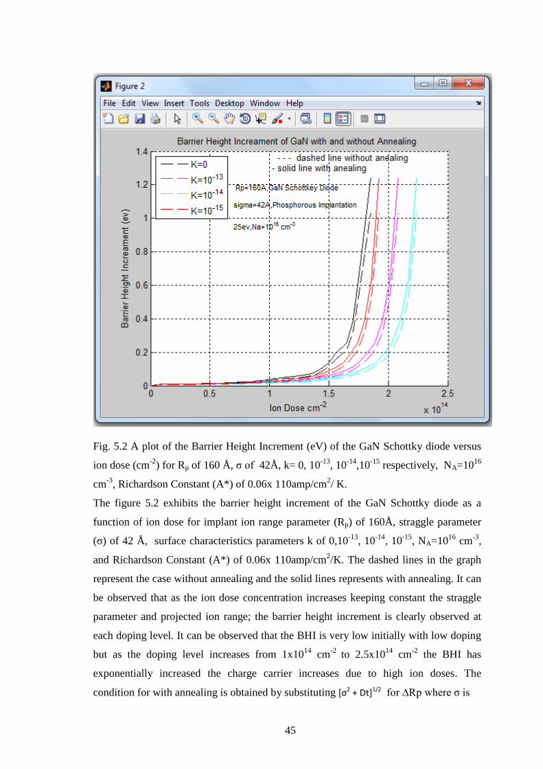
Fig. 5.2 A plot of the Barrier Height Increment (eV) of the GaN Schottky diode versus
ion dose (cm-2
) for Rp of 160 Å, σ of 42Å, k= 0, 10-13
, 10-14
,10-15
respectively, NA=1016
cm-3
, Richardson Constant (A*) of 0.06x 110amp/cm2/ K.
The figure 5.2 exhibits the barrier height increment of the GaN Schottky diode as a
function of ion dose for implant ion range parameter (Rp) of 160Å, straggle parameter
(σ) of 42 Å, surface characteristics parameters k of 0,10-13
, 10-14
, 10-15
, NA=1016
cm-3
,
and Richardson Constant (A*) of 0.06x 110amp/cm2/K. The dashed lines in the graph
represent the case without annealing and the solid lines represents with annealing. It can
be observed that as the ion dose concentration increases keeping constant the straggle
parameter and projected ion range; the barrier height increment is clearly observed at
each doping level. It can be observed that the BHI is very low initially with low doping
but as the doping level increases from 1x10¹⁴
cm-2
to 2.5x10¹⁴
cm-2
the BHI has
exponentially increased the charge carrier increases due to high ion doses. The
condition for with annealing is obtained by substituting [σ2 + Dt]1/2 for ∆Rp where σ is
45
the same straggle parameter and D is the diffusion coefficient and t is the annealing
time. At all the points the consideration of with annealing gives better results than that
of without annealing. This graph was plotted using the equation 26 and Wo has been
evaluated by using iterative method and the value is later substituted in BHI equation.
Fig. 5.3 A plot of the graph the Barrier Height (eV) of the GaN Schottky diode as a
function of ion dose (cm-2
) for Rp of 160 Å, σ of 42 Å, k=0, 10-13
,10-14
, 10-15
, Na=1016
cm-3
, Richardson Constant (A*) = 0.06x 110amp/cm2/ K.
Figure 5.3 presents the barrier height of the GaN Schottky diode as a function of ion
dose (Rp) of 160 Å, straggle parameter (σ) of 42 Å, surface characteristics parameters of
k=0,10-13
,10-14
,10-15
, Na=1016
cm-3
, Richardson Constant (A*) of 0.06x 110amp/cm2/K.
The dashed lines in the graph represent the case without annealing and the solid lines
represents with annealing. It can be observed that as the ion dose concentration
increases along from 1x10¹⁴
cm-2
to 2.5x10¹⁴
cm-2
keeping constant the straggle
46
parameter and projected range; the Barrier height is clearly observed at each doping
level. It can be observe that the BH is very low initially with low doping from 0.3x10¹⁴
cm-2
to 1x10¹⁴
cm-2
but as the doping increases from 1x10¹⁴
cm-2
to 2.5x10¹⁴
cm-2
; the
BH has exponentially increased because of the large carrier concentration. At all the
points the consideration of with annealing gives better results than that of without
annealing. This graph has plotted using the equation 26 and Wo has been determined by
using iterative method and the value is later substituted in BH equation.
This shows that the barrier height is increased with the increase of the ion dose. The
effective barrier height is calculated by the saturation current in the forward bias with
the Richardson constant of A*= 0.06x 110amp/cm2/ K and the active area of 6.86 x 10
-3
cm2. The condition for with annealing is obtained by substituting [σ2 + Dt]1/2 for ∆Rp
where σ is the same straggle parameter and D is the diffusion coefficient and t is the
annealing time. The barrier height enhancement of the GaN Schottky diodes as a
function of ion dose in which the measured barrier height without ion implantation,
ϕBPO= 0.66eV, is used as a reference. It is clearly seen that the theoretical results are in
good agreement to justify with the conventional surface characteristics parameter k
between k = 0 and k = 10-15
V cm-2
, and most of data satisfies k = 10-14
cm2 If the
surface state density is assumed to be equal to 1 x 10¹²
cm2 eV
-1, then the thickness of
the interfacial layer is estimated to be 0.25 Å, which is a reasonable magnitude.
However, a slight fluctuation in fabrication condition is possible, which will give slight
differences in the k value for Schottky barrier diodes with different ion doses.
47
CHAPTER 6
CONCLUSIONS
An analytic model for the barrier height enhancement of the Schottky barrier diode with
low-energy ion implantation has been studied by considering the implanted profile and
the surface properties of the metal-semiconductor contact system. It shows theoretically
that the barrier height enhancement and increment depends on different parameters and
the barrier height enhancement & increment obtained with the consideration of
annealing process is far better than that of without annealing. The most important thing
noticed here is as the ion dose increases the barrier height enhancement is decreased but
the barrier height increment and the barrier height increases as the implanted dose
profile increases. Finally, the theoretical results of the Schottky barrier diodes using
25keV phosphorous ion implantation are used in extreme potential applications and they
make the MESFET device to optimize to the desired Schottky barrier height.
48
REFERENCES
1. Ambipolar charge transport in polymer:fullerene bulk heterojunctions for different
polymer side-chains Appl: Phys. Lett. 101, 123301 (2012). August 2012.
2. Ambipolar charge transport in polymer:fullerene bulk heterojunctions for different
polymer side-chains APL: Org. Electron. Photonics 5, 213 (2012). August 2012.
3. Photocarrier lifetime and transport in silicon supersaturated with sulfur
Appl. Phys. Lett. 101, 111105 (2012). July 2012.
4. Experimental and theoretical investigation of the effect of SiO2 content in gate
dielectrics on work function Shift induced by nanoscale capping layers Appl. Phys.
Lett. 101, 112902 (2012). September 2012.
5. Fixed charge in high-k/GaN metal-oxide-semiconductor capacitor structures
Appl. Phys. Lett. 101, 102905 (2012). June 2012.
6. Akasaki, I., H. Amano, J. Electrochem. Soc. 141, 8 (1994b), 2266-2271. May 2012.
7. Albrecht, J.D., R.P. Wang, P.P. Ruden, M. Farahmand, K.F. Brennan, J. Appl. Phys.
83(9) (1998), 4777-4781. June 2012.
8. Ambacher, O., W. Rieger, P. Ansmann, H. Angerer, T.D. Moustakas, M. Stutzman,
Electron transport characteristics of GaN for high temperature device modeling, Sol.
State Commun. 97(5) (1996), 365-370. May 2012.
9. As, D.J., D. Schikora, A. Greiner, M. Lubbers, J. Mimkes, K. Lischka, p- and n-type
cubic GaN epilayers on GaAs, Phys. Rev. A 54(16) (1996),R11118-R11121. June12.
10. Barker, A.S., Ilegems, M., Infrared Lattice Vibrations and Free-Electron Dispersion
in GaN, Phys. Rev. B 7 (1973) 743. May 2012.
11. Barin, I., O. Knacke, O. Kubaschewski, Thermochemical Properties of Inorganic
Substances, Springer-Verlag, Berlin, 1977. May 2012.
12. Bhapkar, U.V, M.S. Shur, Monte Carlo calculation of velocity-field characteristics of
wurtzite GaN, J. Appl. Phys. 82, 4 (1997), 1649-1655. June 2012.
13. Bloom, S., Harbeke G., Meier E., Ortenburger I.B., Phys. Stat. Solidi 66 (1974), 161-
168. July 2012.
14. Boguslawski, P., E.L. Briggs, J. Bernholc, Native defects in gallium nitride, Phys.
Rev. 51, 23 (1995), 17255-17258. October 2012.
15. Boguslawski, P., J. Bemholc, Acta Phys. Pol A 90 (1996), 735. October 2012.
49
16. Bougrov V., Levinshtein M.E., Rumyantsev S.L., Zubrilov A., in Properties of
Advanced SemiconductorMaterials GaN, AlN, InN, BN, SiC, SiGe. Eds. Levinshtein
M.E., Rumyantsev S.L., Shur M.S., John Wiley & Sons, Inc., New York, 2001, 1-30.
August 2012.
17. Bykhovski, A.D., B.L. Gelmont, M.S. Shur, Elastic strain relaxation and piezoeffect
in GaN-AlN, GaN-AlGaN and GaN-InGaN superlattices, J. Appl. Phys. 81(9)
(1997), 6332-6338. November 2012.
18. Chernyak, L., A. Osinsky, H. Temkin, J.W. Yang, Q. Chen, M.A. Khan, Electron
beam induced current measurements of minority carrier diffusion length in gallium
nitride, Appl. Phys. Lett. 69(17) (1996), 2531-2533. November 2012.
19. Chin, V.W.L, T.L. Tansley, T. Osotchan, Electron mobilities in gallium, indium, and
aluminum nitrides, J. Appl. Phys. 75(11) (1994), 7365-7372. June 2012.
20. Chow, T.P, Ghezzo. SiC power devices. in III-Nitride, SiC, and Diamond Materials
for Electronic Devices. Eds. Gaskill D.K, Brandt C.D. and Nemanich R.J., Material
Research Society Symposium Proceedings, PA.423 (1996), 69-73.July 2012.
21. Crouch, R.K., Debnam, W.J., Fripp, A.L., J. Mater. Sci. 13 (1978) 2358. July 2012.
22. DC Collins, R Avissar - Journal of Climate;(United States), 1994 - osti.gov. June 12.
23. Cunningham, R.D., R.W. Brander, N.D. Knee, D.K. Wickenden, J. Lumin. 5 (1972),
21-31. June 2012.
24. MH El-Axir, MM El-Khabeery - Journal of Materials Processing Technology, 2003
Elsevier, The study of GaN Materials surface characteristics parameters. May 2012.
25. Davydov V.Yu., Yu.E. Kitaev, I.N. Goncharuk, A.N. Smirnov, J. Graul, O.
Semchinova, D. Uffmann, M.B. Smirnov, A.P. Mirgorodsky, R.A. Evarestov.
Phonon dispersion and Raman scattering in hexagonal GaN and AlN, Phys. Rev. B
58(19) (1998) 12899-12907. September 2012.
26. Ding, S.A., S.R. Barman, K. Horn, H. Yang, B.B. Yang, O. Brandt, K. Ploog, and
Valence band discontinuity at a cubic GaN/GaAs heterojunction measured by
synchrotron-radiation photoemission spectroscopy, Appl. Phys. Lett. 70(18) (1997),
2407-2409. October 2012.
27. Dingle, R., D.D. Sell, S.E. Stokowski, P.J. Dean, R.B. Zetterstrom, Absorption,
Reflectance, and Luminescence of GaN Single Crystals, Phys. Rev. B 3(2) (1971),
497-500. October 2012.
28. Gallium Nitride Wikipedia & http://eprints.usm.my/9580/1/ Dingle, R., Ilegems, M.:
Solid State Commun. 9 (1971) 175. October 2012.
50
29. Dmitriev, A.V, Oruzheinikov, A.L. Radiative recombination rates in GaN, InN, AlN
and their solid solutions, in III-Nitride, SiC, and Diamond Materials for Electronic
Devices. Eds. Gaskill D.K, Brandt C.D. and Nemanich R.J., Material Research
Society Symposium Proceedings, Pittsburgh, PA. 423 (1996), 69-73. April 2012.
30. Drory, M.D., J.W. Ager, T. Suski, I. Grzegory, S. Porowski, Hardness and fracture
toughness of bulk single crystal gallium nitride, Appl. Phys. Lett. 69(26) (1996),
4044-4046. May 2012.
31. Dziuba, Z., J. Antoszewski, J.M. Dell, L. Faraone, P. Kozodoy, S. Keller, B. Keller,
S.P. DenBaars, U.K. Mishra, Magnetic field dependent Hall data analysis of electron
transport in modulation-doped AlGaN/GaN heterostructures, J. Appl. Phys. 82(6)
(1997), 2996-3002. June 2012.
32. Edgar, J.H.(ed.). Properties, Applications of Gallium Nitride and Related
semiconductors, EMIS Datareviews Series, N23. INSPEC, London,1999. May 2102.
33. Ejder, E., Phys. Status Solidi (a) 6 (1971), 445-448. May 2012.
34. Fan, J.W., M.F. Li, T.C. Chong, J.B. Xia, Electronic properties of zinc-blende GaN,
AlN, and their alloys Ga1-xAlxN J. Appl. Phys. 79(1) (1996), 188-194. June 2012.
35. Gaska, R., J.W. Yang, A. Osinsky, Q. Chen, M.A. Khan, A.O. Orlov, G.L. Snider,
M.S. Shur, Electron transport in AlGaN-GaN heterostructures grown on 6H-SiC
substrates, Appl. Phys. Lett. 72(6) (1998), 707-709. August 2012.
36. Gaskill, D.K., L.B. Rowland, K. Doverspike, Electrical transport properties of A1N,
GaN and AlGaN, in Properties of Group III Nitrides, ed. Edgar J., EMIS
Datareviews Series, N11, 1995, 101-116. September 2012.
37. Gil, B. (ed.). Group III Nitride Semiconductor Compounds: Physics and
Applications . Series on Semiconductor Science and Technology, 6. Clarendon Press
of the Oxford University Press, Oxford, England, 1998. October 2012.
38. Gorczyca, I., A. Svane, N.E. Christensen, Internet J. Nitride Semicond. Res. 2,
Article 18 (1997). July 2012.
39. Gotz, W., N.M. Johnson, C. Chen, H. Liu, C. Kuo, W. Imler, Activation energies of
Si donors in GaN, Appl. Phys. Lett. 68(22) (1996), 3144 3146. May 2012.
40. Hoist, J., L. Eckey, A. Hoffmann, I. Broser, B. Schottker, D.J. As, D. Schikora, K.
Lischka, Mechanisms of optical gain in cubic gallium nitrite, Appl. Phys. Lett.
72(12) (1998), 1439-1441. August 2012.
41. Ilegems, M., Dingle, R., J. Appl. Phys. 44 (1973) 4234. September 2012.
42. Ilegems,M.,Montgomery,H.C.J. Phys. Chem. Solids 34 (1972) 885. November 2012.
51
43. Ilegems, M., J. Cryst. Growth 13/14 (1972) 360. June 2012.
44. Karch, K., Wagner J.M., Bechstedt F., Bechstedt, Ab initio study of structural,
dielectric, and dynamical properties of GaN, Phys. Rev. B 57(12) (1998), 7043-
7049. June 2012.
45. Kim, J.G, Frenkel A.C., Liu H., Park R.M., Growth by molecular beam epitaxy and
electrical characterization of Si-doped zinc blende GaN films deposited on -SiC
coated (001) Si substrates, Appl. Phys. Lett. 65(1) (1994), 91-93. April 2012.
46. Kolnik, J., Oguzman I.H., Brennan K.F., Wang R., Ruden P.P., Wang, Y. Electronic
transport studies of bulk zincblende and wurtzite phases of GaN based on an
ensemble Monte Carlo calculation including a full zone band structure, J. Appl.
Phys. 78(2) (1995), 1033-1038. July 2012.
47. Leszczynski, M., T. Suski, H. Teisseyre, P. Perlin, I. Grzegory, J. Jun, S. Porowski,
T.D. Moustakas, Thermal expansion of gallium nitride, J. Appl. Phys. 76, 8 (1994),
4909-4911. August 2012.
48. Leszczynski, M., H. Teisseyre, T. Suski, I. Grzegory, M. Bockowski, J. Jun, S.
Porowski, K. Pakula, J.M. Baranowski, C.T. Foxon, T.S. Cheng, Lattice parameters
of gallium nitride, Appl. Phys. Lett. 69(1) (1996), 73-75. October 2012.
49. Lemos, V., Arguello, C.A., Leite, R.C.C, Solid State Commun. 11 (1972) 1351.
50. Lagerstedt, O., Monemar, A., J. Appl. Phys. 45 (1974) 2266. October 2012.
51. Lagerstedt, O., Monemar, A., Variation of lattice parameters in GaN with
stoichiometry and doping, Phys. Rev. B 19 (1979) 3064. September 2012.
52. Madelung, O., ed., Semiconductor: group IV elements and III-V compound. Series
"Data in science and technology", ed. R.Poerschke, Shpringer -Verlag , Berlin,1991,
pp. 164. November 2012.
53. Manchon, D.D., Barker, A.S., Dean, J.P., Zetterstrom, R.B., Solid State Commun. 8
(1970) 1227. November 2012.
54. Martin, G., A. Botchkarev, A. Rockett, H. Morkoc, Valence-band discontinuities of
wurtzite GaN, AlN, and InN heterojunctions measured by x-ray photoemission
spectroscopy, Appl. Phys. Lett. 68(18) (1996), 2541-2543. September 2012.
55. Maruska, H.P, Tietjen, J.J., Appl. Phys. Lett. 15 (1969) 327. October 2012.
56. Mattila, T., Seitsonen, A.P., Nieminen, R.M., Large atomic displacements associated
with the nitrogen antisite in GaN, Phys. Rev. B 54(3) (1996), 1474-1477. September
2012.
57. Mohammad S.N. H.Morkoc, Prog. Quant. Electron. 20 (1996) 361. September 2012.
52
58. Monemar, B., J.P. Bergman, H. Amano, I. Akasaki, T. Detchprohm, K. Hiramatsu,
N. Sawaki, International Symposium on Blue Laser and Light Emiting Diodes,
Chiba University, Japan, March 5-7, 1996. November 2012.
59. Monemar, B., Fundamental energy gap of GaN from photoluminescence excitation
spectra, Phys. Rev. B 10 (1974) 676. November 2012.
60. Monemar, B. Lagerstedt, O, Gislason, H.P., J. Appl. Phys.51 (1980) 625. August 12.
61. Monemar, B,Gislason, H.P., Lagerstedt, O, J. Appl. Phys.51 (1980) 640. August 12.
62. Morkoc, H., S. Strite, G.B. Gao, M.E. Lin, B. Sverdlov, M. Burns, Large-band-gap
SiC, III-V nitride, and II-VI ZnSe-based semiconductor device technologies, J. Appl.
Phys. 76(3) (1994), 1363-1398. October 2012.
63. Morkoc, H. Nitride Semiconductors and Devices, Springer Series in Materials
Science, Vol. 32, Springer, Berlin, 1999. September 2012.
64. Moustakas, T.D., Jacques, I.P. (eds.). Gallium Nitride (GaN) I. Semiconductors and
Semimetals , Vol. 50, Academic Press, San Diego, 1998. November 2012.
65. Muth, J.F, J.H. Lee, I.K. Shmagin, R.M. Kolbas, H.C. Casey, Jr., B.P. Keller, U.K.
Mishra, S.P. DenBaars, Absorption coefficient, energy gap, exciton binding energy,
and recombination lifetime of GaN obtained from transmission measurements, Appl.
Phys. Lett. 71(18) (1997), 2572-2574. August 2012.
66. Nakamura, S.,T. Mukai, M.Senoh,Jpn.J.Appl.Phys.31 (1992), 2883-2888. November
2012.
53
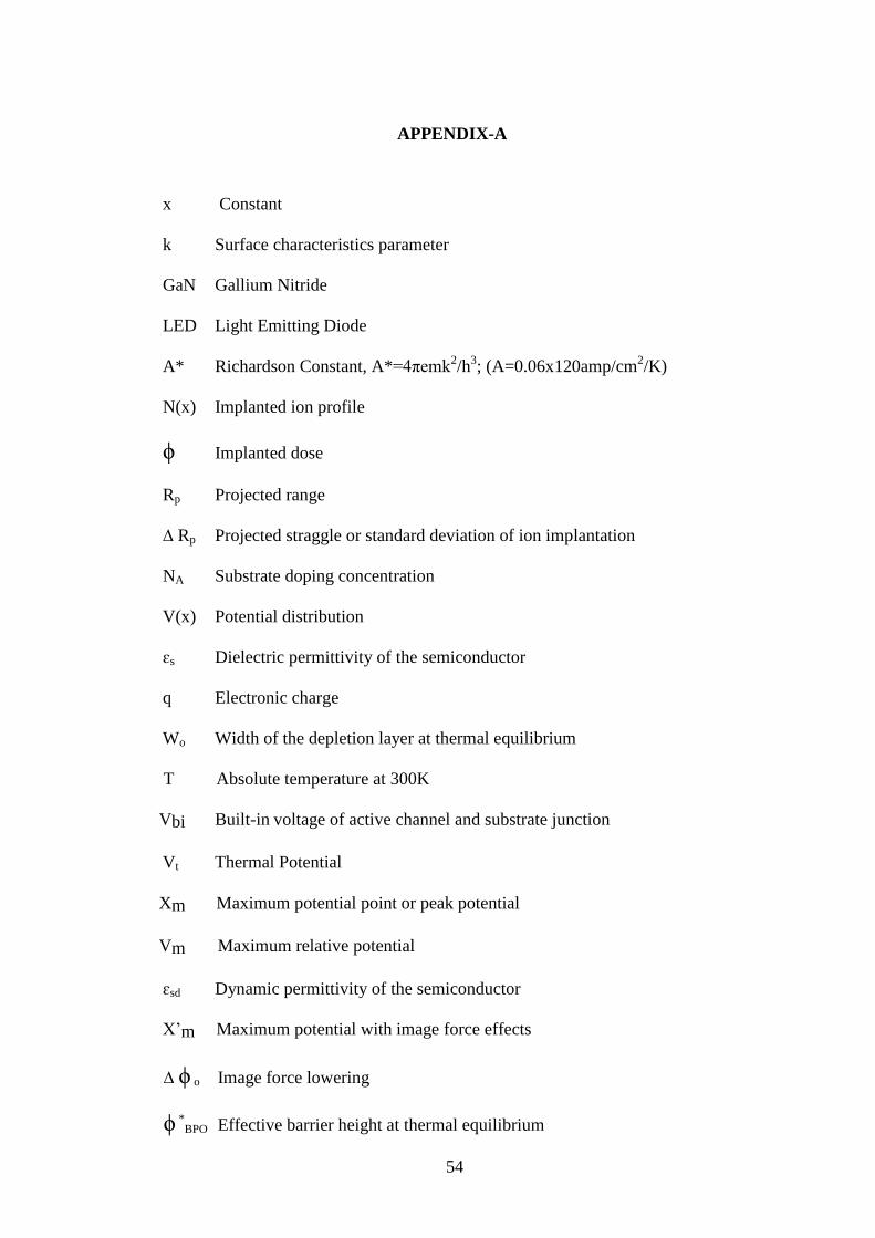
APPENDIX-A
x Constant
k Surface characteristics parameter
GaN Gallium Nitride
LED Light Emitting Diode
A* Richardson Constant, A*=4πemk2/h
3; (A=0.06x120amp/cm
2/K)
N(x) Implanted ion profile
ϕ Implanted dose
Rp Projected range
∆ Rp Projected straggle or standard deviation of ion implantation
NA Substrate doping concentration
V(x) Potential distribution
ɛs Dielectric permittivity of the semiconductor
q Electronic charge
Wo Width of the depletion layer at thermal equilibrium
T Absolute temperature at 300K
Vbi Built-in voltage of active channel and substrate junction
Vt Thermal Potential
Xm Maximum potential point or peak potential
Vm Maximum relative potential
ɛsd Dynamic permittivity of the semiconductor
X’m Maximum potential with image force effects
∆ ϕ o Image force lowering
ϕ *BPO Effective barrier height at thermal equilibrium
54

Vp Potential Difference between valence band edge and the Fermi level in the
neutral p substrate
Qss Charge density in the interface state
Qsc Space charge density in the surface depletion layer at thermal equilibrium
Qs Fixed interface charge density between the semiconductor and the interfacial
layer
q∆ Potential energy across the interfacial layer
EG Energy gap of the semiconductor
qX Electron affinity of the semiconductor
q ϕ M Work function of the metal
ɛi Static permittivity of the interfacial layer
Vbi,o Built-in voltage without the implanted surface layer at thermal equilibrium
C1 Capacitance 1
C2 Capacitance 2
ϕ BPO Barrier height without implanted n layer
∆ ϕoo Image force lowering without the doped surface layer
∆ ϕ BPO Barrier height enhancement
∆ Charge density at the metal surface QM
σ Straggle Parameter
D Diffusion Coefficient
t time constant
55
APPENDIX B
clc ;
clear all;
Na = (10^(16));
q = 1.6021*(10^(-19));
Rp = 1.6*(10^-6);
sigma = 0.42*10^-6;
K=0;
D= 25*10*-6
Es=9.66*8.85*(10^(-14));
Esd = 8.85*(10^(-14));
deltaRp = 0.41*(10^-6);
SIbp = 0.66;
deltaSI = 0.058;
Vp = 0.1;
Mh = (q*Na)/(Es);
Fh = 1/Mh;
Gh = ((2*Es)/(q*Na));
V = Vbi-Vt;
H = (q*si*deltaRp)/((sqrt(2*pi))*Es)
J = (Rp)/(sqrt(2)*deltaRp);
A = q/(16*pi*Esd*(Xm^2));
M = (q*si*Rp)/(2*Es);
Wo= 0.525*10^-6;
Delta = 1;
56
iter = 0;
ITER=0;
Delta1 = 1;
xm=[(10^-4)];
si=[10^10 3*(10^10) 5*(10^10) 8*(10^10) 10^11 2*(10^11) 4*(10^11) 6*(10^11)
8*(10^11) (10^12) 2*(10^12) 4*(10^12) 6*(10^12) 8*(10^12) 10^13];
K=[0 10^-14 5*10^-14 10^-13];
C = 3*10^-4;
Eg=5;
x=6*10^-4;
X=5*10^-4;
SIm=10^-4;
m6=C2((Eg/q) + X - SIm);
Fg=(1-C2)*SI;
jk=(k/q)*Qs;
for j=1:3
for i=1:15
while Delta > 0.1
iter = iter +1;
M = (q*si(i)*Rp)/(2*Es);
F = ((wo(i) - Rp)/(sqrt(2)*deltaRp));
V = H* (exp(-(J^2))-exp(-(F^2)));
Wo(j,i) = sqrt(Gh)*(( (SIbp + deltaSI - Vp)+ ((K(j)*si(i)/2)*(erf(F) + erf(J)))+ V + (
M*(erf(F)+erf(J))))^(1/2));
Wa(j,i) = sqrt(Gh)*(( (SIbp + deltaSI - Vp)+ ((K(j)*si(i)/2)*(erf(F) + erf(J)))+ V + (
57
M*(erf(F)+erf(J))))^(1/2));
Delta = Wo(j,i)-wo(j,i);
DeltaA= Wa(j,i)-wa(j,i);
wo(j,i)=Wo(j,i);
wa(j,i)=Wa(j,i);
end
delta=0;
DeltaA=0;
end
end
for j=1:3
for i =1:15
while Delta1 > 3*10^6
ITER=ITER+1;
N = ((xm(i) - Rp)/(sqrt(2)*sqrt(deltaRp));
Na = ((xm(i) - Rp)/(sqrt(2)*sqrt(SI^2+2*D*t));
A = q/(16*pi*Esd*(xm(i)^2));
Xm(j,i) = Wo(j,i) + Fh*(((M/Rp)*(erf(N) - erf(F)))- A);
Xma(j,i) = Wa(j,i) + Fh*(((M/Rp)*(erf(Na) - erf(F)))- A);
delta1 = Xm(j,i)-xm(j,i);
xm(j,i)=Xm(j,i);
bh(j,i) = (q/(16*pi*Esd*xm(j,i)));
bha(j,i) = (q/(16*pi*Esd*xma(j,i)));
end
Delta1=0;
58
End
for i=1:15
Bhi1(j,i)=m6+Fg+jk+((K(j)*si(i)/2)*(erf(F)+erf(J)))+Mh((xm(j,i)/2)-
(Wo(j,i)*xm(j,i)))+((M/si)*xm)*(erf(((wo(j,i) - Rp)/(sqrt(2)*deltaRp)))-erf(((xm(j,i) –
Rp)/(sqrt(2)*deltaRp)))+H*((q*si(i)*Rp)/(2*Es)));
Bhia1(j,i)=m6+Fg+jk+((K(j)*si(i)/2)*(erf(F)+erf(J)))+Mh((xm(j,i)/2)-
(Wo(j,i)*xm(j,i)))+((M/si)*xm)*(erf(((wo(j,i) - Rp)/(sqrt(2)*deltaRp)))-erf(((xm(j,i) –
Rp)/(sqrt(2)*deltaRp)))+H*((q*si(i)*Rp)/(2*Es)));
bhi(j,i) = bhe-(q/(16*pi*Esd*xm(j,i)));
bhai(j,i) = bhe-(q/(16*pi*Esd*xm(j,i)));
end
end
bhi
for j=1:3
for i=1:4
bhe(j,i) = bhi(j,i)-sibpo;
bhae(j,i) = bhai(j,i)-sibpo;
end
end
hold off;
figure()
hold on;
title('Barrier Height Increament for GaN with and without Annealing ');
xlabel('Ion Dose cm^-^2');
ylabel(' Barrier Height Increament (ev) ');
59
plot(bha,si)
text(8*(10^1^1),0.68,...
'- - - dashed line without Anealing',...
'FontSize',10)
end
bh
for j=1:3
text(8*(10^1^1),0.64,...
'- solid line with Anealing',...
'FontSize',10)
text(5*(10^1^1),0.42,...
' Rp=160A,GaN Schottky Diode',...
'FontSize',8)
text(5*(10^1^1),0.38,...
'deltaRp=42A,Phosphorous Implantation',...
'FontSize',8)
text(8*(10^1^1),0.33,...
' 25ev,Na=10^1^6 cm^-^3',...
'FontSize',8)
hleg2=legend('k=0','k=10^-^1^3','k=10^-^1^4','k=10^-^1^5');
set(hleg2,'location','northwest')
grid on;
hold off;
figure()
hold on;
60
title('Barrier Height for GaN with and without Annealing ');
xlabel('Ion Dose cm^-^2');
ylabel(' Barrier Height (ev) ');
plot(bhai,si);
text(1.42*(10^1^2),1.4,...
'- - - dashed line without Anealing',...
'FontSize',10)
text(1.52*(10^1^2),1.3,...
' - solid line with Anealing',...
'FontSize',10)
text(1.52*(10^1^2),1.2,...
' Rp=160A,GaN Schottky Diode',...
'FontSize',8)
text(1.51*(10^1^2),1.1,...
'deltaRp=42A,Phosphorous Implantation',...
'FontSize',8)
text(1.52*(10^1^2),0.97,...
' 25ev,Na=10^1^6 cm^-3',...
'FontSize',8)
hleg1=legend('k=0','k=10^-^1^3','k=10^-^1^4','k=10^-^1^5');
set(hleg1,'location','northwest')
grid on;
hold off;
figure()
hold on;
61

title('Barrier Height for GaN with and without Annealing ');
xlabel('Ion Dose cm^-^2');
ylabel(' Barrier Height (ev) ');
plot(bhae,si);
text(8*(10^1^1),0.68,...
'- - - dashed line without Anealing',...
'FontSize',10)
text(8*(10^1^1),0.64,...
'- solid line with Anealing',...
'FontSize',10)
text(5*(10^1^1),0.42,...
' Rp=160A,GaN Schottky Diode',...
'FontSize',8)
text(5*(10^1^1),0.38,...
'deltaRp=42A,Phosphorous Implantation',...
'FontSize',8)
text(8*(10^11),0.33,...
' 25ev,Na=10^1^6 cm^-^3',...
'FontSize',8)
hleg2=legend('k=0','k=10^-^1^3','k=10^-^1^4','k=10^-^1^5');
set(hleg2,'location','northwest')
grid on;
hold off;
62

Related Documents