Calculation of bit error rates of optical signal transmission in nano-scale silicon photonic waveguides Jie You A dissertation submitted in partial fulfillment of the requirements for the degree of Doctor of Philosophy of University College London. Department of Electronic and Electrical Engineering University College London July 11, 2017

Welcome message from author
This document is posted to help you gain knowledge. Please leave a comment to let me know what you think about it! Share it to your friends and learn new things together.
Transcript
Calculation of bit error rates of opticalsignal transmission in nano-scale
silicon photonic waveguides
Jie You
A dissertation submitted in partial fulfillment
of the requirements for the degree of
Doctor of Philosophy
of
University College London.
Department of Electronic and Electrical Engineering
University College London
July 11, 2017

2
I, Jie You, confirm that the work presented in this thesis is my own. Where infor-
mation has been derived from other sources, I confirm that this has been indicated in
the work.
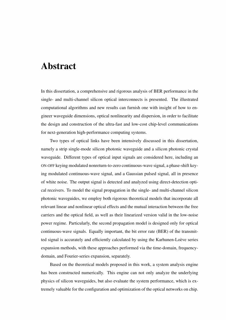
Abstract
In this dissertation, a comprehensive and rigorous analysis of BER performance in the
single- and multi-channel silicon optical interconnects is presented. The illustrated
computational algorithms and new results can furnish one with insight of how to en-
gineer waveguide dimensions, optical nonlinearity and dispersion, in order to facilitate
the design and construction of the ultra-fast and low-cost chip-level communications
for next-generation high-performance computing systems.
Two types of optical links have been intensively discussed in this dissertation,
namely a strip single-mode silicon photonic waveguide and a silicon photonic crystal
waveguide. Different types of optical input signals are considered here, including an
ON-OFF keying modulated nonreturn-to-zero continuous-wave signal, a phase-shift key-
ing modulated continuous-wave signal, and a Gaussian pulsed signal, all in presence
of white noise. The output signal is detected and analyzed using direct-detection opti-
cal receivers. To model the signal propagation in the single- and multi-channel silicon
photonic waveguides, we employ both rigorous theoretical models that incorporate all
relevant linear and nonlinear optical effects and the mutual interaction between the free
carriers and the optical field, as well as their linearized version valid in the low-noise
power regime. Particularly, the second propagation model is designed only for optical
continuous-wave signals. Equally important, the bit error rate (BER) of the transmit-
ted signal is accurately and efficiently calculated by using the Karhunen-Loeve series
expansion methods, with these approaches performed via the time-domain, frequency-
domain, and Fourier-series expansion, separately.
Based on the theoretical models proposed in this work, a system analysis engine
has been constructed numerically. This engine can not only analyze the underlying
physics of silicon waveguides, but also evaluate the system performance, which is ex-
tremely valuable for the configuration and optimization of the optical networks on chip.
Acknowledgements
I would like to express my deep and sincere gratitude to my supervisor Prof. Nico-
lae C. Panoiu. He gave me the opportunity to work in the field of silicon photonic
interconnects and helped me to solve the research obstacles with his scientific insight
and diligence. His talents and unrelenting pursuit for quality make himself the best
role model of scientific researchers for me. I will always appreciate his guidance and
support.
I would like to thank my second supervisor Dr. Philip Watts for constructive ad-
vice, useful discussions and instructions, and for providing the encouragement for my
PhD research. I would also like to thank Prof. John Mitchell for providing insight-
ful comments during the transfer viva. It is helpful to improve my research in a wide
aspect.
I would also like to show my heartfelt gratitude to my colleagues in Prof. Nicolae
C. Panoiu’s group (Dr. Spyros Lavdas, Dr. Martin Weismann, Dan Timbrell, Dr. Jian-
wei You, Qun Ren, Dr. Abiola Oladipo, Dr. Ahmed Al-Jarro, Dr. Wei Wu) for their
friendship and help during my PhD years. Especially for Dr. Spyros Lavdas and Dr.
Jianwei You, who provided me loads of valuable and practical advice when I encoun-
tered difficulties in my study, and who were always ready to support me whenever I
needed help during my research.
In the end, I want to thank my family for their precious love and unconditional
support throughout my whole life.
I really appreciate China Scholarship Council and UCL Dean’s Prize Scholarship
for providing the financial support for my PhD.
Journal articles related to the PhD Dissertation
1. J. You and N. C. Panoiu, “BER in Slow-light and Fast-light Regimes of Silicon
Photonic Crystal Waveguides: A Comparative Study,” IEEE Photon. Technol. Lett.
29, 1093-1096 (2017).
2. J. You and N. C. Panoiu, “Exploiting Higher-order Phase-shift Keying Modulation
and Direct-detection in Silicon Photonic Systems,” Opt. Express 25, 8611-8624 (2017).
3. J. You, S. Lavdas, and N. C. Panoiu, “Comparison of BER in Multi-channel Systems
With Stripe and Photonic Crystal Silicon Waveguides,” IEEE J. Sel. Topics Quantum
Electron. 22, 4400810 (2016).
4. J. You, S. Lavdas, and N. C. Panoiu, “Calculation of BER in Multi-channel Silicon
Optical Interconnects: Comparative Analysis of Strip and Photonic Crystal Waveg-
uides,” Proc. of SPIE 989116, Brussels (2016).
5. J. You and N. C. Panoiu, “Calculation of Bit Error Rates in Optical Systems with
Silicon Photonic Wires,” IEEE J. Quantum Electron. 51, 8400108 (2015).
6. S. Lavdas, J. You, R. M. Osgood, and N. C. Panoiu, “Optical pulse engineering and
processing using optical nonlinearities of nanostructured waveguides made of silicon,”
Proc. SPIE 9546, Active Photonic Materials VII, (2015).
7. J. You and N. C. Panoiu, “An Efficient BER Calculation Approach in Single-channel
Silicon Photonic Interconnects Utilizing Arbitrary RZ-pulse Signals,” J. Lightw. Tech-
nol. (submitted).
Journal articles not directly related to the PhD Dissertation
1. J. W. You, J. You, M. Weismann, and N. C. Panoiu, “Double-Resonant Enhancement
of Third-Harmonic Generation in Graphene Nanostructures,” Phil. Trans. R. Soc. A
375, 20160313 (2017).
Conference contributions related to the PhD Dissertation
1. J. You and N. C. Panoiu, “BER Transmission in Silicon Strip and Photonic Crystal
Systems Utilizing Advanced Modulation Formats,” Photon 16, Leeds (2016).
2. J. You and N. C. Panoiu, “Analysis of BER in Silicon Photonic Systems Utilizing
Higher-order PSK Modulation Formats,” CLEO: Applications and Technology, San
Jose (2016).
3. J. You, S. Lavdas, and N. C. Panoiu, “Calculation of BER in multi-channel silicon
optical interconnects: comparative analysis of strip and photonic crystal waveguides,”
SPIE Photonics Europe, Brussels (2016).
4. J. You, S. Lavdas, and N. C. Panoiu, “BER Calculation in Photonic Systems Con-
taining Strip or Photonic Crystal Silicon Waveguides,” Asia Communications and
Photonic Conference, HongKong (2015).
5. N. C. Panoiu, S. Lavdas, and J. You, “Optical pulse engineering using nonlinearities
of nanostructured silicon photonic wires,” 24th International Laser Physics Workshop
(LPHYS’15), Shanghai (2015). (Invited)
6. N. C. Panoiu, S. Lavdas, J. You, and R. M. Osgood, “Optical pulse engineering and
processing using nonlinearities of tapered and photonic crystal waveguides made of
silicon,” Active Photonic Materials VII, San Diego (2015).

LIST OF NOTATIONS AND ACRONYMS
4PSK 4-ary phase-shift keying
8PSK 8-ary phase-shift keying
ASK-PSK combination of intensity and phase modulation
αin intrinsic loss
αFC free-carrier loss
BER bit-error rate
β mode propagation constant
β2 group velocity dispersion coefficient
CW continuous-wave
c speed of light in vacuum (2.99792458×10⁸ m/s)
ε0 electric permittivity of vacuum (8.854×10⁻¹²F/m)
e electron charge (1.6021766208×10⁻¹⁹ C)
FC free-carrier
FCD free-carrier dispersion
FCA free-carrier absorption
FEM finite-element method
FFT Fast Fourier Transformation
FWM four-wave mixing
F Fourier transform
GV group velocity
GVD group-velocity dispersion
HPC high-performance computing
h reduced Planck constant (1.05457162853×10⁻³⁴ kg/s)
KLSE Karhunen-Loeve Series Expansion
κ overlap integral between the waveguide core and optical mode
MZI Mach-Zehnder interferometer
MGF moment-generating function
NLSE nonlinear Schrodinger equation
NoC networks-on-chip
LIST OF NOTATIONS AND ACRONYMS
NRZ nonreturen-to-zero
n refractive index
δnFC free-carrier induced refractive index charge
OOK On-Off keying
ODE ordinary differential equation
PSK phase-shift keying
PhC photonic crystal
γ waveguide nonlinear coefficient
Γ effective nonlinear susceptibility
Si silicon
SOI silicon-on-insulator
Si-PhW silicon photonic waveguide
Si-PhCW silicon photonic crystal waveguide
SSFM Split-step Fourier Method
SL slow-light
SPM self phase modulation
TOD third-order dispersion
TPA two-photon absorption
VCSEL vertical-cavity surface-emitting lasers
WDM wavelength-division multiplexing
XPM cross-phase modulation
χ(3) third-order optical susceptibility
ZGVD zero group velocity dispersion
Contents
Contents . . . . . . . . . . . . . . . . . . . . . . . . . . . . . . . . . . . . . . 9
List of Figures . . . . . . . . . . . . . . . . . . . . . . . . . . . . . . . . . . . 13
List of Tables . . . . . . . . . . . . . . . . . . . . . . . . . . . . . . . . . . . . 23
1 Introduction . . . . . . . . . . . . . . . . . . . . . . . . . . . . . . . . . . 24
1.1 Main Objectives of the Work . . . . . . . . . . . . . . . . . . . . . . . 27
1.2 Outline . . . . . . . . . . . . . . . . . . . . . . . . . . . . . . . . . . . 29
Bibliography . . . . . . . . . . . . . . . . . . . . . . . . . . . . . . . . . . . 32
2 Background . . . . . . . . . . . . . . . . . . . . . . . . . . . . . . . . . . . 38
2.1 Introduction . . . . . . . . . . . . . . . . . . . . . . . . . . . . . . . . 38
2.2 Optical Properties of Silicon Nanowire Waveguide . . . . . . . . . . . . 40
2.2.1 Frequency Dispersion of Silicon Nanowire Waveguide . . . . . 40
2.2.2 Nonlinear Optical Properties of Silicon Nanowire Waveguide . . 42
2.2.3 Free Carrier Dynamics in Silicon Nanowire Waveguide . . . . . 44
2.3 Types of Silicon Photonic Waveguides . . . . . . . . . . . . . . . . . . 44
2.3.1 Strip Silicon Photonic Waveguides . . . . . . . . . . . . . . . . 45
2.3.2 Silicon Photonic Crystal Waveguides . . . . . . . . . . . . . . . 48
2.4 Silicon Photonic System Models . . . . . . . . . . . . . . . . . . . . . 50
2.5 Optical Signal Modulation Formats . . . . . . . . . . . . . . . . . . . . 53
2.6 Theory of Optical Signal Propagation in Silicon Waveguides . . . . . . 54
2.6.1 Theory of Single-wavelength Optical Signal Propagation . . . . 54
2.6.2 Theory of Multi-wavelength Optical Signal Propagation . . . . 58
2.7 Linearized Theoretical Model for CW Noise Dynamics . . . . . . . . . 59
2.7.1 Single-channel CW Noise Linearization . . . . . . . . . . . . . 60
9
10
2.7.2 Multi-channel CW Noise Linearization . . . . . . . . . . . . . 62
2.8 Computational Algorithms of Signal Propagation . . . . . . . . . . . . 64
2.8.1 Split Step Fourier Method . . . . . . . . . . . . . . . . . . . . 64
2.8.2 Computational Solvers for Ordinary Differential Equations . . . 67
Bibliography . . . . . . . . . . . . . . . . . . . . . . . . . . . . . . . . . . . 69
3 Mathematical Concepts Used in BER Calculation . . . . . . . . . . . . . 79
3.1 Introduction . . . . . . . . . . . . . . . . . . . . . . . . . . . . . . . . 79
3.2 Time-domain Karhunen-Loeve Expansion Method . . . . . . . . . . . . 80
3.3 Frequency-domain Karhunen-Loeve Expansion . . . . . . . . . . . . . 85
3.4 Fourier-series Karhunen-Loeve Expansion . . . . . . . . . . . . . . . . 88
3.5 Saddle-point Approximation Approach for Probability Density Func-
tion Calculation . . . . . . . . . . . . . . . . . . . . . . . . . . . . . . 90
Bibliography . . . . . . . . . . . . . . . . . . . . . . . . . . . . . . . . . . . 94
4 Numerical Implementation of Main Computational Methods . . . . . . . 96
4.1 Introduction . . . . . . . . . . . . . . . . . . . . . . . . . . . . . . . . 96
4.2 Program Flow for System Analysis Models . . . . . . . . . . . . . . . 97
4.3 Algorithms in the System Evaluation Engine . . . . . . . . . . . . . . . 101
4.3.1 Full Algorithm of Signal Propagation . . . . . . . . . . . . . . 101
4.3.2 Linearized Algorithm of Signal Propagation . . . . . . . . . . . 103
4.3.3 Time-domain KLSE Algorithm in BER Calculation . . . . . . . 104
4.3.4 Frequency-domain KLSE Algorithm in BER Calculation . . . . 106
4.3.5 Fourier-series KLSE Algorithm in BER Calculation . . . . . . . 107
4.3.6 Comparative Study of Alternative Algorithms . . . . . . . . . . 109
4.4 Conclusions . . . . . . . . . . . . . . . . . . . . . . . . . . . . . . . . 112
Bibliography . . . . . . . . . . . . . . . . . . . . . . . . . . . . . . . . . . . 113
5 Calculation of Bit Error Rates in Optical Systems with Strip Silicon Pho-
tonic Wires . . . . . . . . . . . . . . . . . . . . . . . . . . . . . . . . . . . 115
5.1 Introduction . . . . . . . . . . . . . . . . . . . . . . . . . . . . . . . . 115
5.2 Theoretical Signal Propagation Model in Strip Silicon Photonic Wires . 116
5.3 Calculation of BER . . . . . . . . . . . . . . . . . . . . . . . . . . . . 121
11
5.4 Results and Discussion . . . . . . . . . . . . . . . . . . . . . . . . . . 121
5.5 Conclusion . . . . . . . . . . . . . . . . . . . . . . . . . . . . . . . . 126
Bibliography . . . . . . . . . . . . . . . . . . . . . . . . . . . . . . . . . . . 128
6 Slow-light and Fast-light Regimes of Silicon Photonic Crystal Waveg-
uides: A Comparative Study . . . . . . . . . . . . . . . . . . . . . . . . . 129
6.1 Introduction . . . . . . . . . . . . . . . . . . . . . . . . . . . . . . . . 129
6.2 Optical Properties of Silicon Photonic Crystal Waveguides . . . . . . . 130
6.3 Optical Signal Propagation Approach . . . . . . . . . . . . . . . . . . . 131
6.4 Results and Anaylsis . . . . . . . . . . . . . . . . . . . . . . . . . . . 134
6.5 Conclusion . . . . . . . . . . . . . . . . . . . . . . . . . . . . . . . . 137
Bibliography . . . . . . . . . . . . . . . . . . . . . . . . . . . . . . . . . . . 138
7 Exploiting Higher-order PSK Modulation and Direct-detection in
Single-channel Silicon Photonic Systems . . . . . . . . . . . . . . . . . . . 139
7.1 Introduction . . . . . . . . . . . . . . . . . . . . . . . . . . . . . . . . 139
7.2 Theory of Propagation of Optical Signals in Silicon Waveguides . . . . 140
7.3 Optical Direct-detection Receivers for High-order PSK Modulated Sig-
nals . . . . . . . . . . . . . . . . . . . . . . . . . . . . . . . . . . . . 141
7.4 Methods for Analysis of Direct-detection of PSK and ASK-PSK Signals 143
7.4.1 General Case . . . . . . . . . . . . . . . . . . . . . . . . . . . 143
7.4.2 Application to 8PSK Modulation Format . . . . . . . . . . . . . 145
7.5 Results and Discussion . . . . . . . . . . . . . . . . . . . . . . . . . . 147
7.6 Conclusion . . . . . . . . . . . . . . . . . . . . . . . . . . . . . . . . 152
Bibliography . . . . . . . . . . . . . . . . . . . . . . . . . . . . . . . . . . . 154
8 Performance Evaluation in Multi-channel Systems With Strip and Pho-
tonic Crystal Silicon Waveguides . . . . . . . . . . . . . . . . . . . . . . . 156
8.1 Introduction . . . . . . . . . . . . . . . . . . . . . . . . . . . . . . . . 156
8.2 Description of the Photonic Waveguides . . . . . . . . . . . . . . . . . 157
8.3 Theory of Multi-wavelength Optical Signal Propagation in Silicon Wires 160
8.4 Time and Frequency Domain Karhunen-Loeve Series Expansion Methods165
8.5 Performance Evaluation for Multi-channel Systems . . . . . . . . . . . 166

12
8.6 Conclusion . . . . . . . . . . . . . . . . . . . . . . . . . . . . . . . . 170
Bibliography . . . . . . . . . . . . . . . . . . . . . . . . . . . . . . . . . . . 172
9 Single-channel Silicon Photonic Interconnects Utilizing RZ Pulsed Signals 173
9.1 Introduction . . . . . . . . . . . . . . . . . . . . . . . . . . . . . . . . 173
9.2 Theory of PRBS Optical Pulse Propagation in Silicon Waveguides . . . 174
9.3 Theoretical Approach for BER Calculation . . . . . . . . . . . . . . . . 176
9.4 Results and Discussion . . . . . . . . . . . . . . . . . . . . . . . . . . 177
9.5 Conclusion . . . . . . . . . . . . . . . . . . . . . . . . . . . . . . . . 186
Bibliography . . . . . . . . . . . . . . . . . . . . . . . . . . . . . . . . . . . 188
10 Conclusions and Future work . . . . . . . . . . . . . . . . . . . . . . . . . 189
10.1 Contributions . . . . . . . . . . . . . . . . . . . . . . . . . . . . . . . 190
10.2 Future Prospects . . . . . . . . . . . . . . . . . . . . . . . . . . . . . . 193
Appendices . . . . . . . . . . . . . . . . . . . . . . . . . . . . . . . . . . . . . 195
A Gauss-Hermite Algorithm . . . . . . . . . . . . . . . . . . . . . . . . . . . 195
B Fifth-order Runge-Kutta Algorithm . . . . . . . . . . . . . . . . . . . . . 197
C Golden Section Algorithm . . . . . . . . . . . . . . . . . . . . . . . . . . . 199
List of Figures
2.1 Structure of four types of Si waveguides, including (a) a strip waveg-
uide, (b) a rib waveguide, (c) a slot waveguide and (d) a photonic crystal
waveguide. . . . . . . . . . . . . . . . . . . . . . . . . . . . . . . . . 39
2.2 The generic structure of strip Si photonic waveguides. . . . . . . . . . . 40
2.3 (a) A strip Si photonic waveguide with uniform cross section; (b) A Si
photonic crystal waveguide. . . . . . . . . . . . . . . . . . . . . . . . . 45
2.4 Dispersion maps of propagation constant β for certain widths of Si-
PhWs with fixed hight of h = 250nm. . . . . . . . . . . . . . . . . . . 45
2.5 Dispersion maps of (a) group index ng = c/vg; (b) GVD coefficient
β2; (c) TOD coefficient β3; (d) fourth-order coefficient β4; for certain
widths of Si-PhWs with constant height h = 250nm. . . . . . . . . . . . 46
2.6 Real (a) and imaginary (b) part of nonlinear coefficients for Si-PhW
waveguides with several widths and a specific hight of h = 250nm. . . . 47
2.7 Projected band structure. Dark yellow and green ares correspond to
slab leaky and guiding modes, respectively. The red and blue curves
represent the y-even and y-odd guiding mode of the 1D waveguides.
Light grey shaded regions correspond to SL regime, ng > 20. . . . . . . 48
2.8 (a), (b), (c), and (d) Frequency dependence of waveguide dispersion
coefficients ng = c/vg, β2, β3 and β4, respectively, determined for the
Mode A (red) and Mode B (blue). Light green, blue, and brown shaded
regions correspond to SL regime, ng > 20. . . . . . . . . . . . . . . . . 49
2.9 Real (a) and imaginary (b) parts of nonlinear coefficients for Si-PhCW
waveguides versus wavelength, in cases of Mode A (red) and Mode B
(blue). Light green, blue, and brown shaded regions correspond to SL
regime, ng > 20. . . . . . . . . . . . . . . . . . . . . . . . . . . . . . . 50
13
14
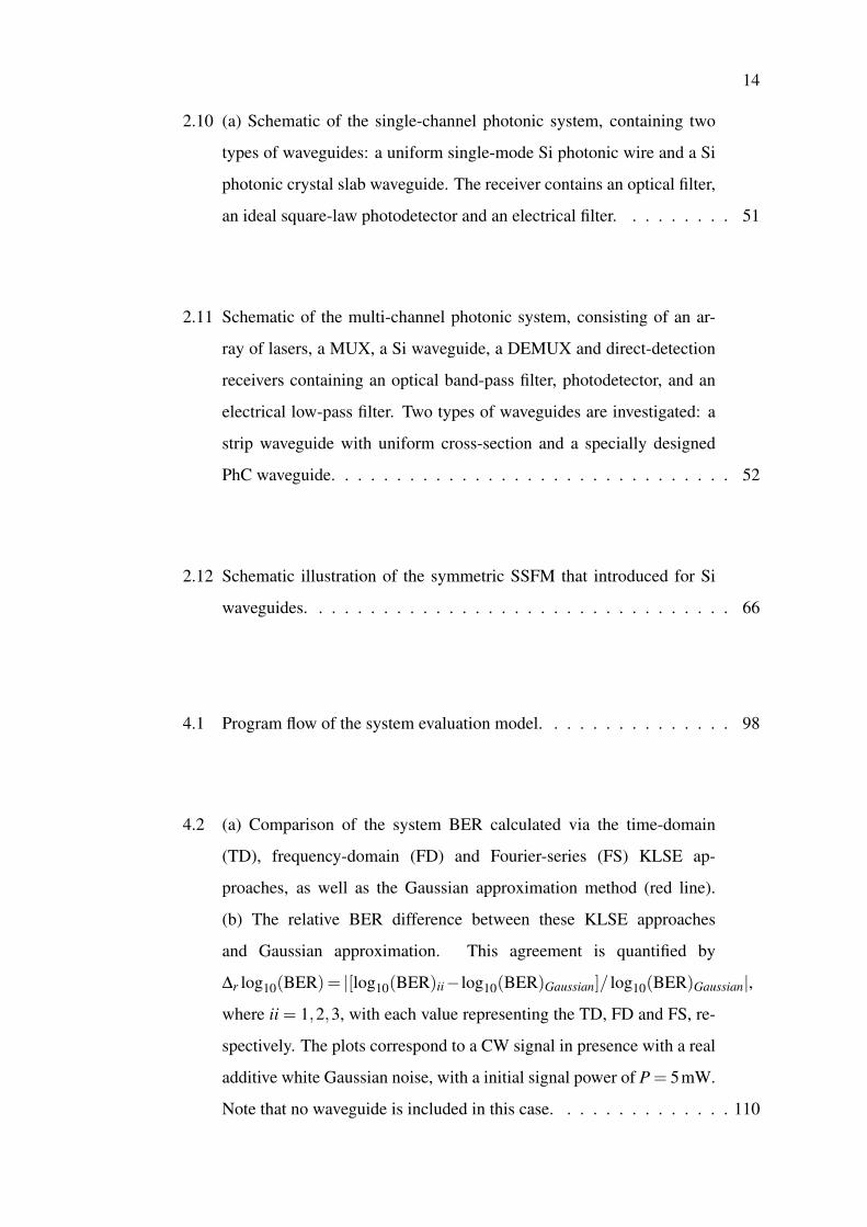
2.10 (a) Schematic of the single-channel photonic system, containing two
types of waveguides: a uniform single-mode Si photonic wire and a Si
photonic crystal slab waveguide. The receiver contains an optical filter,
an ideal square-law photodetector and an electrical filter. . . . . . . . . 51
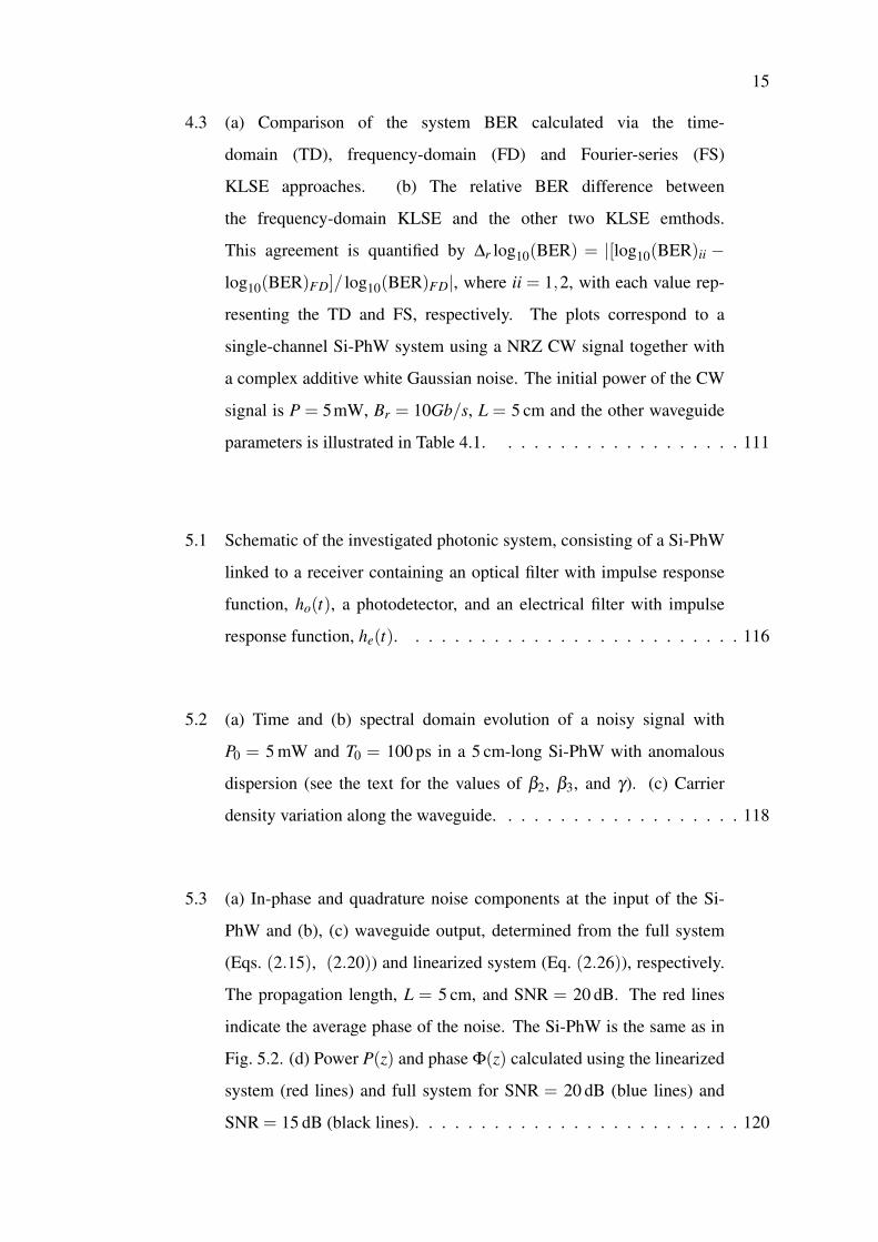
2.11 Schematic of the multi-channel photonic system, consisting of an ar-
ray of lasers, a MUX, a Si waveguide, a DEMUX and direct-detection
receivers containing an optical band-pass filter, photodetector, and an
electrical low-pass filter. Two types of waveguides are investigated: a
strip waveguide with uniform cross-section and a specially designed
PhC waveguide. . . . . . . . . . . . . . . . . . . . . . . . . . . . . . . 52
2.12 Schematic illustration of the symmetric SSFM that introduced for Si
waveguides. . . . . . . . . . . . . . . . . . . . . . . . . . . . . . . . . 66
4.1 Program flow of the system evaluation model. . . . . . . . . . . . . . . 98
4.2 (a) Comparison of the system BER calculated via the time-domain
(TD), frequency-domain (FD) and Fourier-series (FS) KLSE ap-
proaches, as well as the Gaussian approximation method (red line).
(b) The relative BER difference between these KLSE approaches
and Gaussian approximation. This agreement is quantified by
∆r log10(BER)= |[log10(BER)ii−log10(BER)Gaussian]/ log10(BER)Gaussian|,
where ii = 1,2,3, with each value representing the TD, FD and FS, re-
spectively. The plots correspond to a CW signal in presence with a real
additive white Gaussian noise, with a initial signal power of P = 5mW.
Note that no waveguide is included in this case. . . . . . . . . . . . . . 110
15
4.3 (a) Comparison of the system BER calculated via the time-
domain (TD), frequency-domain (FD) and Fourier-series (FS)
KLSE approaches. (b) The relative BER difference between
the frequency-domain KLSE and the other two KLSE emthods.
This agreement is quantified by ∆r log10(BER) = |[log10(BER)ii −
log10(BER)FD]/ log10(BER)FD|, where ii = 1,2, with each value rep-
resenting the TD and FS, respectively. The plots correspond to a
single-channel Si-PhW system using a NRZ CW signal together with
a complex additive white Gaussian noise. The initial power of the CW
signal is P = 5mW, Br = 10Gb/s, L = 5 cm and the other waveguide
parameters is illustrated in Table 4.1. . . . . . . . . . . . . . . . . . . 111
5.1 Schematic of the investigated photonic system, consisting of a Si-PhW
linked to a receiver containing an optical filter with impulse response
function, ho(t), a photodetector, and an electrical filter with impulse
response function, he(t). . . . . . . . . . . . . . . . . . . . . . . . . . 116
5.2 (a) Time and (b) spectral domain evolution of a noisy signal with
P0 = 5 mW and T0 = 100 ps in a 5 cm-long Si-PhW with anomalous
dispersion (see the text for the values of β2, β3, and γ). (c) Carrier
density variation along the waveguide. . . . . . . . . . . . . . . . . . . 118
5.3 (a) In-phase and quadrature noise components at the input of the Si-
PhW and (b), (c) waveguide output, determined from the full system
(Eqs. (2.15), (2.20)) and linearized system (Eq. (2.26)), respectively.
The propagation length, L = 5 cm, and SNR = 20 dB. The red lines
indicate the average phase of the noise. The Si-PhW is the same as in
Fig. 5.2. (d) Power P(z) and phase Φ(z) calculated using the linearized
system (red lines) and full system for SNR = 20 dB (blue lines) and
SNR = 15 dB (black lines). . . . . . . . . . . . . . . . . . . . . . . . . 120
16
5.4 System BER vs. SNR, calculated for Si-PhWs with normal (solid line)
and anomalous (dashed line) dispersion (see the text for the values of
β2, β3, and γ). The waveguide length, L = 5 cm. The dotted line in-
dicates the BER in the case of a system without the silicon waveguide.
The horizontal black solid line corresponds to a BER of 10−9. . . . . . 122
5.5 System BER vs. SNR, calculated for several different values of the
waveguide loss coefficient, αi. The panels (a) and (b) correspond to
waveguides A (β2 > 0) and B (β2 < 0), respectively. In all simulations
P0 = 5 mW and L = 5 cm. The horizontal black solid line corresponds
to a BER of 10−9. . . . . . . . . . . . . . . . . . . . . . . . . . . . . . 122
5.6 System BER vs. SNR, calculated for Si-PhWs with different width,
w. The waveguide parameters for all widths are given in Table 5.2. In
all cases P0 = 5 mW and L = 5 cm. The horizontal black solid line
indicates a BER of 10−9. . . . . . . . . . . . . . . . . . . . . . . . . . 124
5.7 Contour maps of log10(BER) vs. power and SNR. (a), (b) correspond
to Si-PhWs with normal and anomalous dispersion, respectively, the
waveguides being the same as in Fig. 5.4. The black contours corre-
spond to BER = 10−9. . . . . . . . . . . . . . . . . . . . . . . . . . . 124
5.8 Maps of log10(BER) vs. γ ′ and SNR. (a), (b) correspond to Si-PhWs
with normal and anomalous dispersion, respectively. In both cases
γ ′′/γ ′ = 0.3, P0 = 5 mW, and L = 5 cm. The black contours indicate
a BER of 10−9. . . . . . . . . . . . . . . . . . . . . . . . . . . . . . . 125
5.9 Contour maps of log10(BER) vs. waveguide length and SNR. Panels (a)
and (b) correspond to Si-PhWs with normal and anomalous dispersion,
respectively, the waveguides being the same as in Fig. 5.4. The input
power is P0 = 5 mW. The black contours correspond to a BER of 10−9. 126
6.1 (a) Schematic of the photonic system, containing a Si-PhCW and a
direct-detection receiver composed of an optical filter, ho(t), a photode-
tector, and an electrical filter, he(t). (b) Mode dispersion diagram of the
Si-PhCW, with grey bands indicating the SL spectral domains ng > 20. . 130
17
6.2 (a), (b), (c) Wavelength dependence of ng, β2, and γ ′ and γ ′′, respec-
tively, determined for mode A (red lines) and mode B (blue lines). The
shaded areas correspond to the SL regime, defined by the relation ng > 20.131
6.3 (a) In-phase and quadrature noise components at the input of the Si-
PhCW. (b), (c) the same as in (a), but determined at the waveguide out-
put in the FL and SL regimes. Second, third, and fourth row of panels
show the time domain, spectral domain, and carrier density evolution
of a noisy signal with P0 = 10mW and T0 = 100ps in a 500 µm-long
Si-PhCW, respectively, with the left (right) panels corresponding to the
FL (SL) regime. . . . . . . . . . . . . . . . . . . . . . . . . . . . . . . 133
6.4 Top panels show the system BER calculated for the Si-PhCW with FC
dynamics included (left) and by neglecting them (right). Bottom panels
show the eye diagrams corresponding to ng = 8.64 (left) and ng = 27.7
(right), both at SNR = 25 dB. In all panels, P0 = 10 mW and L = 500 µm.135
6.5 (a), (b) System BER vs. SNR, calculated for different P0, in the SL
(ng = 27.7) and FL (ng = 8.64) regimes, respectively. The horizontal
black line indicates a BER of 10−9. . . . . . . . . . . . . . . . . . . . . 136
7.1 Schematics of the Si photonic system investigated in this work. It con-
tains a Si waveguide and a direct-detection receiver with bi-level electri-
cal decisions. The receiver has two branches, an intensity-detection and
a phase-detection branch, with the latter consisting of N Mach-Zehnder
interferometers. Two types of waveguides are investigated: one is a
strip waveguide with uniform cross-section with height, h = 250nm,
and width, w = 900nm and the other one is a PhC waveguide with lat-
tice constant, a = 412nm, hole radius, r = 0.22a, and slab thickness,
h = 0.6a. . . . . . . . . . . . . . . . . . . . . . . . . . . . . . . . . . . 140
7.2 Constellation diagrams of the investigated signal modulation formats.
(a), (b), (c), (d), (e), (f), are for 2PSK, 4PSK, 8PSK, 16PSK, A2PSK,
and A4PSK modulation, respectively. (g), (h), (i) The decision bound-
aries for 4PSK, 8PSK, and 16PSK modulation formats. . . . . . . . . . 142
18
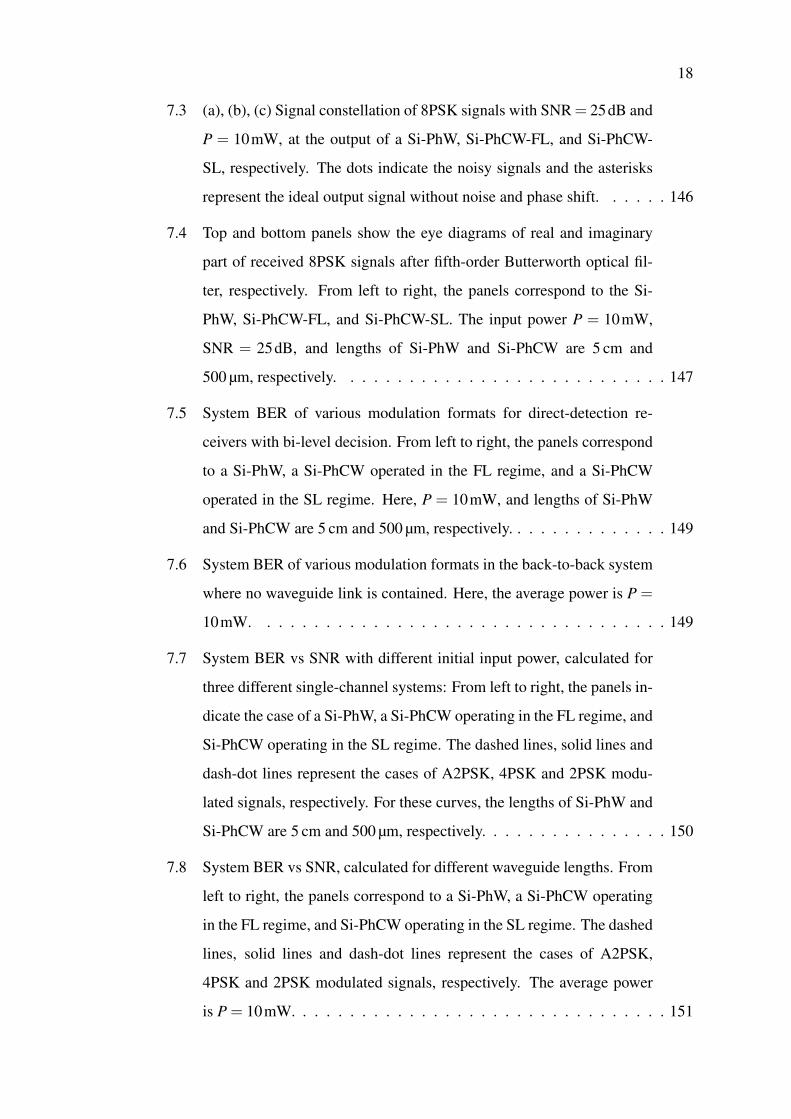
7.3 (a), (b), (c) Signal constellation of 8PSK signals with SNR = 25dB and
P = 10mW, at the output of a Si-PhW, Si-PhCW-FL, and Si-PhCW-
SL, respectively. The dots indicate the noisy signals and the asterisks
represent the ideal output signal without noise and phase shift. . . . . . 146
7.4 Top and bottom panels show the eye diagrams of real and imaginary
part of received 8PSK signals after fifth-order Butterworth optical fil-
ter, respectively. From left to right, the panels correspond to the Si-
PhW, Si-PhCW-FL, and Si-PhCW-SL. The input power P = 10mW,
SNR = 25dB, and lengths of Si-PhW and Si-PhCW are 5 cm and
500 µm, respectively. . . . . . . . . . . . . . . . . . . . . . . . . . . . 147
7.5 System BER of various modulation formats for direct-detection re-
ceivers with bi-level decision. From left to right, the panels correspond
to a Si-PhW, a Si-PhCW operated in the FL regime, and a Si-PhCW
operated in the SL regime. Here, P = 10mW, and lengths of Si-PhW
and Si-PhCW are 5 cm and 500 µm, respectively. . . . . . . . . . . . . . 149
7.6 System BER of various modulation formats in the back-to-back system
where no waveguide link is contained. Here, the average power is P =
10mW. . . . . . . . . . . . . . . . . . . . . . . . . . . . . . . . . . . 149
7.7 System BER vs SNR with different initial input power, calculated for
three different single-channel systems: From left to right, the panels in-
dicate the case of a Si-PhW, a Si-PhCW operating in the FL regime, and
Si-PhCW operating in the SL regime. The dashed lines, solid lines and
dash-dot lines represent the cases of A2PSK, 4PSK and 2PSK modu-
lated signals, respectively. For these curves, the lengths of Si-PhW and
Si-PhCW are 5 cm and 500 µm, respectively. . . . . . . . . . . . . . . . 150
7.8 System BER vs SNR, calculated for different waveguide lengths. From
left to right, the panels correspond to a Si-PhW, a Si-PhCW operating
in the FL regime, and Si-PhCW operating in the SL regime. The dashed
lines, solid lines and dash-dot lines represent the cases of A2PSK,
4PSK and 2PSK modulated signals, respectively. The average power
is P = 10mW. . . . . . . . . . . . . . . . . . . . . . . . . . . . . . . . 151
19
7.9 BER calculated for several system receiver configurations. From left to
right, the panels correspond to a Si-PhW, a Si-PhCW operated in the FL
regime, and Si-PhCW operated in the SL regime. In all cases, an 8PSK
modulation format is considered. The electrical filter is chosen as fifth
Bessel filter, whereas the optical filter is a Lorentzian filter (red line),
Gaussian filter (black line), super-Gaussian filter (blue line), and sixth-
order Butterworth filter (purple line). For these curves, P= 10mW, and
L = 5cm (L = 500µm) for the Si-PhW (Si-PhCW). . . . . . . . . . . . 152
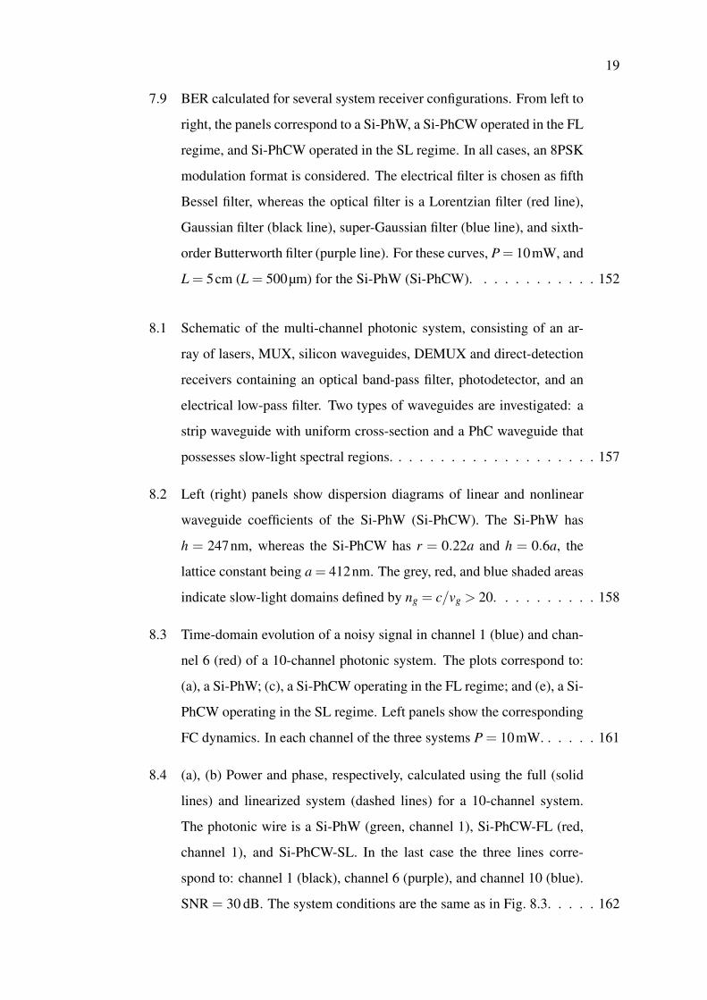
8.1 Schematic of the multi-channel photonic system, consisting of an ar-
ray of lasers, MUX, silicon waveguides, DEMUX and direct-detection
receivers containing an optical band-pass filter, photodetector, and an
electrical low-pass filter. Two types of waveguides are investigated: a
strip waveguide with uniform cross-section and a PhC waveguide that
possesses slow-light spectral regions. . . . . . . . . . . . . . . . . . . . 157
8.2 Left (right) panels show dispersion diagrams of linear and nonlinear
waveguide coefficients of the Si-PhW (Si-PhCW). The Si-PhW has
h = 247nm, whereas the Si-PhCW has r = 0.22a and h = 0.6a, the
lattice constant being a = 412nm. The grey, red, and blue shaded areas
indicate slow-light domains defined by ng = c/vg > 20. . . . . . . . . . 158
8.3 Time-domain evolution of a noisy signal in channel 1 (blue) and chan-
nel 6 (red) of a 10-channel photonic system. The plots correspond to:
(a), a Si-PhW; (c), a Si-PhCW operating in the FL regime; and (e), a Si-
PhCW operating in the SL regime. Left panels show the corresponding
FC dynamics. In each channel of the three systems P = 10mW. . . . . . 161
8.4 (a), (b) Power and phase, respectively, calculated using the full (solid
lines) and linearized system (dashed lines) for a 10-channel system.
The photonic wire is a Si-PhW (green, channel 1), Si-PhCW-FL (red,
channel 1), and Si-PhCW-SL. In the last case the three lines corre-
spond to: channel 1 (black), channel 6 (purple), and channel 10 (blue).
SNR = 30 dB. The system conditions are the same as in Fig. 8.3. . . . . 162
20
8.5 (a) In-phase and quadrature noise components at the input of the 10-
channel Si-PhW, Si-PhCW-FL and Si-PhCW-SL systems. (b), (c)
Noise components at the output of channel 1 of the Si-PhW and Si-
PhCW-FL systems, respectively, determined from the linearized sys-
tem Eq. (2.30). (d), (e), (f) Noise output in channel 1, channel 6, and
channel 10, respectively, in the Si-PhCW-SL system. SNR = 30 dB.
The system conditions are the same as in Fig. 8.3. . . . . . . . . . . . . 163
8.6 Comparison of the system BER calculated via the time- and frequency-
domain KL expansion method. The plots correspond to channel 6
in an 8-channel system containing a Si-PhW (green), Si-PhCW op-
erating in the FL regime (red), and a Si-PhCW operating in the FL
regime (blue). Initial signal power in each channel is P = 5mW. The
agreement between the two methods is quantified by ∆r log10(BER) =
[log10(BER)FD− log10(BER)T D]/ log10(BER)FD. . . . . . . . . . . . . 165
8.7 System BER for channel 2 vs. SNR, calculated for systems with dif-
ferent number of channels. From top to bottom, the panels correspond
to a Si-PhW, a Si-PhCW operating in the FL regime, and a Si-PhCW
operating in the SL regime. . . . . . . . . . . . . . . . . . . . . . . . . 167
8.8 Maps of log10(BER) vs. power and SNR, calculated for three different
8-channel systems: from top to bottom, the panels correspond to a Si-
PhW, a Si-PhCW operating in the FL regime, and a Si-PhCW operating
in the SL regime. Left and right panels correspond to channel 1 and
channel 8, respectively. Black curves correspond to log10(BER) =−9. . 168
8.9 Maps of log10(BER) vs. waveguide length and SNR, calculated for
three different 8-channel systems: from top to bottom, the panels cor-
respond to a Si-PhW, a Si-PhCW operating in the FL regime, and a
Si-PhCW operating in the SL regime. Left and right panels correspond
to channel 1 and channel 8, respectively. The input power in each chan-
nel is P = 5mW. Black curves correspond to log10(BER) =−9. . . . . 169
21
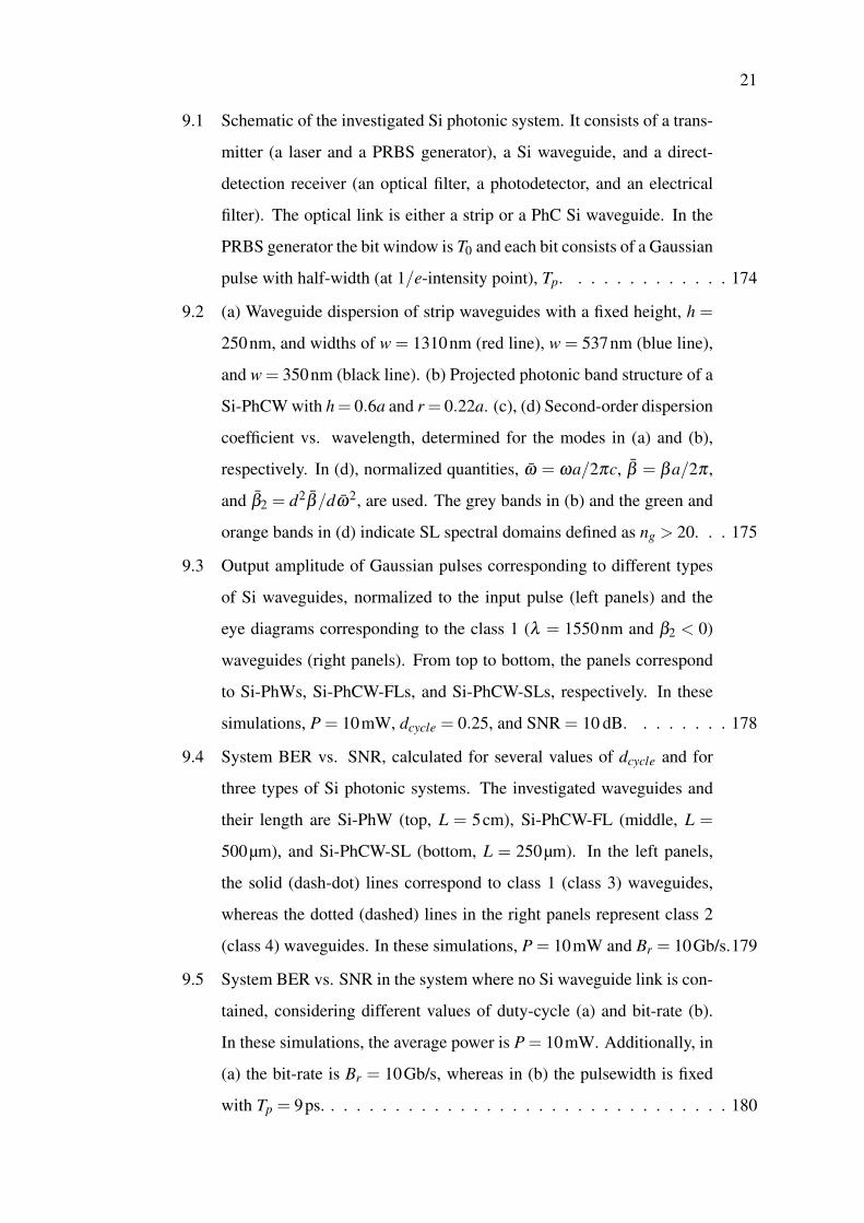
9.1 Schematic of the investigated Si photonic system. It consists of a trans-
mitter (a laser and a PRBS generator), a Si waveguide, and a direct-
detection receiver (an optical filter, a photodetector, and an electrical
filter). The optical link is either a strip or a PhC Si waveguide. In the
PRBS generator the bit window is T0 and each bit consists of a Gaussian
pulse with half-width (at 1/e-intensity point), Tp. . . . . . . . . . . . . 174
9.2 (a) Waveguide dispersion of strip waveguides with a fixed height, h =
250nm, and widths of w = 1310nm (red line), w = 537nm (blue line),
and w = 350nm (black line). (b) Projected photonic band structure of a
Si-PhCW with h= 0.6a and r = 0.22a. (c), (d) Second-order dispersion
coefficient vs. wavelength, determined for the modes in (a) and (b),
respectively. In (d), normalized quantities, ω = ωa/2πc, β = βa/2π ,
and β2 = d2β/dω2, are used. The grey bands in (b) and the green and
orange bands in (d) indicate SL spectral domains defined as ng > 20. . . 175
9.3 Output amplitude of Gaussian pulses corresponding to different types
of Si waveguides, normalized to the input pulse (left panels) and the
eye diagrams corresponding to the class 1 (λ = 1550nm and β2 < 0)
waveguides (right panels). From top to bottom, the panels correspond
to Si-PhWs, Si-PhCW-FLs, and Si-PhCW-SLs, respectively. In these
simulations, P = 10mW, dcycle = 0.25, and SNR = 10 dB. . . . . . . . 178
9.4 System BER vs. SNR, calculated for several values of dcycle and for
three types of Si photonic systems. The investigated waveguides and
their length are Si-PhW (top, L = 5cm), Si-PhCW-FL (middle, L =
500µm), and Si-PhCW-SL (bottom, L = 250µm). In the left panels,
the solid (dash-dot) lines correspond to class 1 (class 3) waveguides,
whereas the dotted (dashed) lines in the right panels represent class 2
(class 4) waveguides. In these simulations, P = 10mW and Br = 10Gb/s.179
9.5 System BER vs. SNR in the system where no Si waveguide link is con-
tained, considering different values of duty-cycle (a) and bit-rate (b).
In these simulations, the average power is P = 10mW. Additionally, in
(a) the bit-rate is Br = 10Gb/s, whereas in (b) the pulsewidth is fixed
with Tp = 9ps. . . . . . . . . . . . . . . . . . . . . . . . . . . . . . . . 180
22
9.6 BER vs. SNR, determined for different Br and Si photonic systems.
From top to bottom, the panels correspond to Si-PhWs (L = 5cm),
Si-PhCW-FLs (L = 500µm), and Si-PhCW-SLs (L = 250µm). The
dash-dot, dashed, solid, and dotted lines correspond to class 1, class 2,
class 3, and class 4 waveguides, respectively. In all cases, P = 10mW
and Tp = 9ps. . . . . . . . . . . . . . . . . . . . . . . . . . . . . . . . 181
9.7 Dependence of BER on the input power and bit-rate for four strip
waveguide systems: (a) Si-PhW-1, (b) Si-PhW-2, (c) Si-PhW-3, and
(d) Si-PhW-4. In all cases, SNR = 12dB, L = 5cm, and Tp = 9ps. . . . 182
9.8 Constant-level curves corresponding to BER = 10−9. The average
power is 5mW (solid lines), 7mW (dashed lines), and 9mW (dash-dot
lines). The red, blue, green, and black curves correspond to Si-PhW-1,
Si-PhW-2, Si-PhW-3, and Si-PhW-4 cases, respectively. In all calcula-
tion, L = 5cm and Br = 10Gb/s. . . . . . . . . . . . . . . . . . . . . . 183
9.9 Contour maps of log10(BER) vs. power and pulse duty-cycle, cal-
culated for four Si-PhCW systems at λ = 1550nm. The top (bot-
tom) panels correspond to Si-PhCW-FLs with L = 500µm (Si-PhCW-
SLs with L = 250µm), whereas the left (right) panels correspond to
class 1 (class 2) Si-PhCWs. In all case, SNR = 12dB, P = 10mW, and
Br = 10Gb/s. . . . . . . . . . . . . . . . . . . . . . . . . . . . . . . . 184
9.10 Variation of the system BER with the bit-rate. Top (bottom) panel
corresponds to FL (SL) regime, in both cases the wavelength being
λ = 1550nm. The red and blue curves correspond to class 1 Si-
PhCWs, whereas black and magenta curves to class 2 Si-PhCWs. The
values of SNR and average power are indicated in the legends, whereas
Tp = 9ps. . . . . . . . . . . . . . . . . . . . . . . . . . . . . . . . . . 185
List of Tables
4.1 Main parameters for a Si-PhW used in Fig. 4.3. . . . . . . . . . . . . . 111
5.1 Main parameters for the Si-PhWs used in our simulations. . . . . . . . . 117
5.2 Waveguide parameters used to obtain the results presented in Fig. 5.6 . . 124
6.1 Main parameters for the Si-PhCW-FLs used in our simulations. . . . . . 132
6.2 Main parameters for the Si-PhCW-SLs used in our simulations. . . . . . 132
6.3 Characteristic length of FCA and TPA for different group-index. . . . . 135
7.1 The optical parameters of silicon waveguides used in numerical simu-
lations. . . . . . . . . . . . . . . . . . . . . . . . . . . . . . . . . . . . 141
8.1 Main parameters for the 8-channel Si-PhW waveguide used in our sim-
ulations. . . . . . . . . . . . . . . . . . . . . . . . . . . . . . . . . . . 159
8.2 Main parameters for the 8-channel Si-PhCW-FL waveguide used in our
simulations. . . . . . . . . . . . . . . . . . . . . . . . . . . . . . . . . 159
8.3 Main parameters for the 8-channel Si-PhCW-SL waveguide used in our
simulations. . . . . . . . . . . . . . . . . . . . . . . . . . . . . . . . . 159
9.1 Silicon waveguide parameters used to in all our simulations . . . . . . . 176
B.1 Cash-Karp paramters for embedded Runge-Kutta method. . . . . . . . . 197
B.2 Dormand-Prince paramters for embedded Runge-Kutta method. . . . . 198
23
Chapter 1
Introduction
Photonics can be viewed as a field that involves light-related technologies and applica-
tions, which smoothly blends the subjects of physics and engineering. During the last
few decades, photonics has spread into almost all areas of modern life and cutting-edge
technologies, including telecommunications, computing, medicine and robotics. Con-
currently, with the development of photonics in our knowledge-based society, rapidly
increasing growth of data traffic in networks driven by bandwidth-intensive applica-
tions, such as the widespread use of social networking, video streaming in mobile ap-
plications, and cloud services, is creating increasingly stringent demand for bandwidth,
which can be effectively addressed by deploying broadband optical communications
solutions [1]. Internet data centers and high-performance computing (HPC) systems
are just two examples of markets where photonic technologies can play a major role.
Optical interconnects are viewed as a promising alternative to the commonly used
copper wires [2], due to their unique features of high capacity, large transparency win-
dow, and fundamentally low energy consumption. Furthermore, the optical commu-
nications have already been deployed in the metro and long haul networks during the
last two decades [3], and will penetrate into the development of next-generation in-
formation networks [4]. In fact, rack-to-rack (1m ∼ 100m) [5] and board-to-board
(10cm ∼ 1m) [6] communications already contain optical networks in some fastest
HPC systems. It is envisioned that this trend of using optical communications at an
ever-smaller scale will continue to grow, so that in future HPC platforms will play the
main role in node-to-node and even intra-node communications [7, 8].
Then silicon-on-insulator (SOI) material platform is regarded as one of the most
appealing approaches to integrate photonics into chip-level networks, due to its unique
25
characteristics listed below:
1. High index contrast. The relatively large refractive index difference between
silicon (Si) (nSi ∼ 3.46) and cladding, which can be either buried-oxide substrate
(nSi02 ∼ 1.45) or air (nair = 1), makes possible to tightly confine and guide light
in optical waveguides with deep-subwavelength transverse dimensions [9–11].
2. Broad-band transparency window. Silicon is transparent beyond 1.2 µm up to the
mid-Infrared region, which allows for ultrahigh bandwidth data communications
[12].
3. Dispersion and nonlinearity engineering. The strong light confinement enables
to greatly engineer the dispersion of Si waveguides, either by changing the
transverse size of the waveguides or by nano-patterning them. In addition, Si
possesses very large third-order nonlinearities in a broad spectral range, which
means that key active optical functionalities, such as Raman amplification, self-
phase modulation (SPM), cross-phase modulation (XPM), four-wave mixing
(FWM), and pulse self-steepening can be easily implemented by using this opti-
cal material [11, 13].
4. Good compatibility with the CMOS electric circuitries [14–16]. All basic com-
ponents of the desired photonic networks have already been implemented in
the SOI platforms, including optical amplifiers [17, 18], modulators [19–21],
switches [22–24], receivers [25, 26], and frequency converters [27, 28].
5. High thermal conductivity and high optical damage threshold [29]. Silicon en-
compasses optical damage threshold of 1−4 GWcm−2 and thermal conductivity
of 148 Wm−1 K−1, facilitating excellent mid-Infrared Raman lasers and ampli-
fiers [30].
Importantly, the recent breakthroughs in the photonic device integration [31, 32] make
Si photonics more pervasive for the chip-level information networks.
In addition to the constant drive towards downscaling the size of optical intercon-
nects, an equally daunting challenge pertaining to exascale computing systems is to
decrease the per-bit power consumption to levels that allow cost-effective operation.
26
Photonic structures provide a versatile solution that addresses both these issues, as they
allow one to engineer both the linear and nonlinear properties of the optical intercon-
nects. To be more specific, by nano-patterning Si photonic strip waveguides (Si-PhWs)
and photonic crystal (PhC) waveguides (Si-PhCWs), optical properties of these struc-
tures can be tuned. A salient example of such structure are Si-PhCWs [33, 34], which
are commonly implemented by introducing a line defect in a periodic dielectric ma-
trix. In particular, the group-velocity (GV), vg, of optical signals propagating in PhC
waveguides can be reduced by orders of magnitude, which leads to a dramatic change
of the linear and nonlinear optical properties of photonic devices [35–37]. One key
consequence of this so-called slow-light (SL) effect is that the characteristic disper-
sion and nonlinear lengths, and implicitly the device footprint, could decrease signif-
icantly. On the other hand, optical losses and nonlinear effects, such as SPM, XPM
and two-photon absorption (TPA), which impair the quality of transmitted optical sig-
nals, are enhanced in the SL regime, too. Moreover, if Si waveguides are employed in
wavelength-division-multiplexing (WDM) enabled applications, photogenerated free-
carriers (FCs) provide an additional mechanism for inter-channel cross-talk, which is
an example of a detrimental effect that is enhanced in the SL regime. The advantages
provided by the SL operation of photonic devices are therefore not a priori transpar-
ent, especially if multi-channel operation is considered, and consequently an in-depth
analysis of these ideas is needed.
Furthermore, intensive investigation of main optical phenomena in Si photonic
waveguides have been carried out experimentally and theoretically in recent years. Ra-
man scattering in the Si waveguides was firstly observed in 2002 [38], followed by
the exploration of anti-Stokes Raman scattering (CARS) in 2003 [39]. Simultaneously,
several other important nonlinear phenomena were discovered, i.e., SPM [40], TPA
[41], XPM [42], FWM [43], supercontinuum generation [44], and soliton generation
[45]. In addition, research efforts have also been devoted to linear effects like optical
loss [46], GV dispersion (GVD) [47], and third-order dispersion (TOD) [48].
Up to now, even though almost all components of Si photonics ecosystem exist,
including the fundamental study (e.g., UCSB), design (e.g., Photon Design), foundries
(e.g., ST), devices (e.g., LIGHTWIRE), systems (e.g, IBM, CISCO, HUAWEI), and
end-customers (e.g., Facebook), the large scale manufacturing of Si photonic waveg-
27
uides for the optical chips is still in its infancy [49]. It will be of critical importance
to have a set of tools suitable for estimating the bit error rate (BER) of optical data
streams transmitted among different nodes of the nextworks-on-chip (NoC). In partic-
ular, a reliable characterization of the performance photonic NoC can be achieved via
a bottom-up approach, in which one first determines at the physical layer the optical
signal impairments introduced by each of the components of the NoC, are firstly deter-
mined at the physical layer, this information being then used to evaluate at the system
level the overall performance of the photonic network. Therefore, the aim of this disser-
tation is to propose a rigorous theoretical and computational software platform, which
can not only facilitate the physics of Si photonic waveguides, but also evaluate the BER
performance of photonic systems under different circumstance. In the next section, the
main objectives of this dissertation will be explained.
1.1 Main Objectives of the WorkThe two main objectives of this dissertation will be discussed in this section. Aiming
at developing a set of theoretical models and computational tools for the analysis of
optical signal transmission in silicon photonic systems, both cases of continuous-wave
(CW) and pulsed optical signals will be extensively investigated. Achieving each of
the objectives amounts to employing different mathematical algorithms and numerical
implementations, which will be explained in details below.
To start with, I will use a rigorous theoretical model to describe the propagation
of optical signals in a single-mode silicon-on-insulator strip waveguide. In particular, a
superposition of a nonreturn-to-zero (NRZ) ON-OFF keying (OOK) modulated optical
signal and an additive white Gaussian noise is selected as the optical input, which
can also be analyzed by utilizing a linearized propagation model. These models fully
incorporate all essential linear and nonlinear optical effects. The BER of the output
signal will be measured via the time-domain Karhunen-Loeve series expansion (KLSE)
method after direct-detection. For a better understanding of how waveguide dispersion
and nonlinearity determine the signal quality, I will present a comparative study of the
influence of the normal and anomalous dispersion regimes in Si-PhWs on the system
BER.
Subsequently, I will present an in-depth investigation of the NRZ CW optical sig-
28
nal transmission in the optical system containing PhC Si waveguides operating in the
slow- and fast-light regimes. Particularly, SL spectral regions can be accessed by sig-
nificantly reduced GV, vg. This results in increased waveguide dispersion and effective
waveguide nonlinearity, as these physical quantities scale with vg as v−1g and v−2
g , re-
spectively. Correpsondingly, the influence of SL effects on the optical field and carrier
dynamics will be also thoroughly explored.
In addition, I will also theoretically and numerically evaluate the BER in Si pho-
tonic systems employing high-order phase-shift keying (PSK) modulation formats. Par-
ticularly, both Si-PhWs and Si-PhCWs are included in the investigated systems, as well
as direct-detection receivers suitable to detect PSK and amplitude-shaped PSK signals.
Notably, the system BER will be calculated by applying a frequency-domain approach
based on the KLSE. The emphasis of this comprehensive analysis will be on how the
optical power, types of PSK modulation, and group-velocity characterize the transmis-
sion BER, as well as the relation between the influence of these factors on BER and
system nonlinearity.
Furthermore, I will illustrate a multi-wavelength optical signal propagating either
in a Si-PhW or in a Si-PhCW, with each channel consisting of a CW NRZ OOK mod-
ulated signal. As an extension of the single-wavelength signal transmission case, M
sets of coupled linearized equations will be utilized to describe M-wavelength signals
co-propagation. Both time- and frequency-domain KLSE methods will be employed to
calculate the BER of the transmitted signal. The numerical simulations will highlight
the importance of carefully selecting the waveguide types and dimensions, number of
channels, and optical input power, when taking the system performance into consider-
ation.
The second objective of this dissertation is to extensively study the performance of
Si photonic systems operating in the pulsed regimes. To fulfill this goal, I will employ
the full theoretical model to characterize the single-wavelength optical pulse propa-
gation in a Si-PhW or a Si-PhCW, and a Fourier-series KLSE method to estimate the
system BER. Then, I will demonstrate the impact of signal parameters (pulsewidth, data
rate, wavelength, power) and waveguide parameters (dispersion regions, SL regimes)
on the quality of transmitted signal. One remarkable feature of the rigorous models
mentioned above is that they can account for all types of optical signals and be easily
29
extended to the multi-channel system evaluation cases.
A related point to consider is that the performance analysis engine, which will be
described in this dissertation, is of the capability to characterize more complicated pho-
tonic systems. To be more specific, this engine can be easily extended to other types of
optical waveguides, waveguide-based devices and chip-scale optical networks of prac-
tical interest. Moreover, the formalism of signal propagation theory can be modified
to incorporate additional nonlinear effects such as FWM and stimulated Raman scat-
tering, which could become important optical effects in nanoscale waveguides. A brief
summary of the whole dissertation will be given in the next section.
1.2 OutlineChapter 2 presents the literature review of Si photonics, optical characterization of Si
waveguides, and the configuration of the photonic systems investigated in this work.
Further to that, rigorous theoretical models for the single- and multi-wavelength signal
propagation will be presented, aiming at incorporating all relevant linear and nonlinear
optical effects and the mutual interaction between FCs and the optical field. Addition-
ally, the linearized version of the full propagation model mentioned above is presented
for the case of CW signals, which is validated in the low-noise power regime. There-
after, the numerical routines regarding the full and linearized propagation models will
be described. Specifically, the former models employ the Split-step Fourier Method
(SSFM) plus a fifth-order Runge-Kutta method, whereas a Matlab built-in function is
used to solve ordinary differential equations (ODEs) in the latter models. This chapter
provides the physical background and signal propagation routines for the remaining
chapters in this dissertation.
Chapter 3 describes the computational methods for the BER calculation in Si pho-
tonic systems. Firstly, a concise literature review of the BER evaluation methods will
be introduced. Next, three types of KLSE approaches (the time-domain, frequency-
domain and Fourier-series) which are adopted in this dissertation, will be described in
details. I will then present a numerical technique called saddle-point approximation,
which is applied to derive the system BERs based on the moment-generating function
(MGF) calculated with these KLSE methods. This chapter can be viewed as containing
all the essential implementation related to the system evaluation models.
30
Chapter 4 describes the numerical implementation of the system evaluation mod-
els, including the signal propagation theory in Chapter 2 and BER calculation methods
in Chapter 3. This numerical and computational tool is capable of accounting for differ-
ent types of Si waveguides, various formats of signal modulation , and varied numbers
of transmission channels. The program flow of this system evaluation engine will be
illustrated in this chapter, followed by the specification of the key parameters and the
characterization of the numerical algorithms utilized in the computer program.
In Chapter 5 and Chapter 6, I discuss the transmission of an OOK modulated
optical CW signal in the single-channel optical systems containing a Si-PhW and a
Si-PhCW, respectively, in presence of an additive white Gaussian noise. In these two
chapters, both full and linearized theoretical single-channel CW models are adopted
to describe the propagation of the optical signal in Si waveguides, whereas the time-
domain KLSE method is used to evaluate the BER. Importantly, in Chapter 5, I com-
prehensively investigate the influence of parameters characterizing the Si-PhWs on the
transmission BER, while I present and discuss the dependence of BER on the key sys-
tem parameters in Chapter 6, including group-velocity, input power, and signal-to-noise
ratio.
In Chapter 7, I focus on the evaluation of a higher-order PSK modulated opti-
cal CW signal transmitted in the single-channel strip and photonic crystal Si systems.
The modified nonlinear Schrodinger equation (NLSE) that governs the propagation of
the noisy PSK signals in Si waveguides is employed, as well as the frequency-domain
KLSE method for BER calculation. Moreover, the description of the advanced mod-
ulation formats and the details of direct-detection are also presented in this chapter.
The system performance corresponding to several PSK formats is rigorously analyzed,
considering varied key system parameters.
For completeness, in Chapter 8, I present a comparative analysis of the perfor-
mance of the multi-channel photonic systems containing a Si-PhW or a Si-PhCW, with
each channel propagating the OOK modulated CW signals. The optical properties of
the investigated Si waveguides are described in this chapter. Furthermore, the system of
M coupled NLSE equations is applied to measure the propagation of a M-wavelength
noisy signal in these two Si waveguides, taking into account the nonlinear phenomena
like XPM and the overall FCs accumulated from these signals, whereas the time- and
31
frequency-domain formulation of the KLSE method are used to compute system BER.
The impact of white Gaussian noise on BER is thoroughly studied, in presence of Kerr
nonlinearity, frequency dispersion, and FCs.
What follows next is the investigation of the single-channel Si photonic inter-
connects exploiting optical pulsed signals, as discussed in Chapter 9. Firstly, the full
single-channel pulse propagation model is utilized to describe the evolution of a single-
channel pseudorandom binary sequence (PRBS) noisy Gaussian signal. The details of
the investigated Si Photonic waveguides are also exhibited in Chapter 8, considering
frequencies (1550nm, 1300nm), dispersion regions (normal, anomalous), and GV (SL,
FL). Then, the Fourier-series KLSE method is employed to evaluate the system per-
formance. Several simulation results regarding the pulse properties and waveguide
parameters are displayed in this chapter as well, in order to provide a reference for the
photonic systems operating in the pulsed regime.
In Chapter 10, I summarize the main conclusions of this dissertation, and stresses
the main contributions of this dissertation to the field of Si optical interconnects. Future
perspectives of this work are also included in this chapter.
32
Bibliography[1] Y. A. Vlasov, “Silicon CMOS-Integrated Nano-Photonics for Computer and Data
Communications Beyond 100G,” Commun. Mag.50, S67-S72 (2012).
[2] A. Benner, D. M. Kuchta, P. K. Pepeljugoski, R. A. Budd, G. Hougham, B. V.
Fasano, K. Marston, H. Bagheri, E. J. Seminaro, H. Xu, D. Meadowcroft, M.
H. Fields, L. McColloch,M. Robinson, F.W. Miller, R. Kaneshiro, R. Granger,
D. Childers, and E. Childers, “Optics for High-Performance Servers and Super-
computers,” Optical Fiber Communication Conf. and Expo. (OFC), OTuH1, 1-3
(2010).
[3] B. Ciftcioglu, “Intra-Chip Free-Space Optical Interconnect: System, Device, In-
tegration and Prototyping,” Ph. D. Thesis (University of Rochester, 2012).
[4] R. Ho, K. W. Mai, and M. A. Horowitz, “The future of wires,” Proc. IEEE 89,
490-504 (2001).
[5] J. W. Parker, P. J. Ayliffe, T. V. Clapp, M. C. Geear, P. M. Harrison, and R. G.
Peall, “Multifibre Bus for rack-to-rack intreconnects based on opto-hybrid trna-
mitter/receiver array pair,” Electron. Lett. 28, 801-803 (1992).
[6] D. V. Plant, M. B. Venditti, E. Laprise, J. Faucher, K. Razavi, M. Chteauneuf, A.
G. Kirk, and J. S. Aheran, “256-Channel Bidirectional Optical Interconnect Using
VCSELs and Photodiodes on CMOS,” IEEE J. Lightwave Technol. 19, 1093-1103
(2002).
[7] W. Green, S. Assefa, A. Rylyakov, C. Schow, F. Horst, and Y. Vlasov, “CMOS
integrated silicon nanophotonics: Enabling technology for exascale computation,”
Semicon, Tokyo (2010). Available at www.research.ibm.com/photonics.
[8] J. A. Kash, A. F. Benner, F. E. Doany, D. M. Kuchta, B. G. Lee, P. K. Pepeljugoski,
L. Schares, C. L. Schow, and M. Taubenblatt, “Optical Interconnects in Exascale
Supercomputers,” 23rd Annual Meeting of the IEEE Photonics Society, 483-484
(2010).
33
[9] K. K. Lee, D. R. Lim, H. C. Luan, A. Agarwal, J. Foresi, and L. C. Kimerling,
“Effect of size and roughness on light transmission in a Si/SiO2 waveguide: Ex-
periments and model,” Appl. Phys. Lett. 77, 1617-1619 (2000).
[10] R. U. Ahmad, F. Pizuto, G. S. Gamarda, R. L. Espinola, H. Rao, and R. M. Os-
good, “Ultracompact cornermirrors and T-branches in silicon-on-insulator,” IEEE
Photon. Technol. Lett. 14, 65-67 (2002).
[11] R. M. Osgood, N. C. Panoiu, J. I. Dadap, X. Liu, X. Chen, I-W Hsieh, E. Dulkeit,
W. M. J. Green, and Y. A. Vlassov, “Engineering nonlinearities in nanoscale op-
tical systems: physics and applications in dispersion engineered silicon nanopho-
tonics wires,” Adv. Opt. Photon. 1, 162-235 (2009).
[12] B. G. Lee, X. Chen, A. Biberman, X. Liu, I-W. Hsieh, C. Chou, J. I. Dadap, F.
Xia, W. M. J. Green, L. Sekaric, Y. A. Vlasov, R. M. Osgood, and K. Bergman,
“Ultrahigh-Bandwidth Silicon Photonic Nanowire Waveguides for On-Chip Net-
works,” IEEE Photon. Technol. Lett. 20, 398-400 (2008).
[13] Q. Lin, Oskar J. Painter, and G. P. Agrawal, “Nonlinear optical phenomena in
silicon waveguides: modeling and applications,” Opt. Express 15, 16604-16644
(2007).
[14] T. Barwicz, H. Byun, and F. Gan, C. W. Holzwarth, M. A. Popovic, P. T. Rakich,
M. R. Watts, E. P. Ippen, F. X. Kartner, H. I. Smith, J. S. Orcutt, R. J. Ram, V. Sto-
janovic, O. O. Olubuyide, J. L. Hoyt, S. Spector, M. Geis, M. Grein, T. Lyszczarz,
and J. U. Yoon, “Silicon photonics for compact, energy-efficient interconnects,”
J. Opt. Commun. Netw. 6, 63-73 (2007).
[15] J. S. Orcutt, A. Khilo, C. W. Holzwarth, M. A. Popovic, H. Li, J Sun, T. Boni-
field, R. Hollingsworth, F. X. Kartner, H. I. Smith, V. Stojanovic, R. J. Ram,
“Nanophotonic integration in state-of-the-art CMOS foundries,” Opt. Express 19,
2335-2346 (2011).
[16] A. V. Krishnamoorthy, X. Zheng, G. Li, J. Yao, T. Pinguet, A. Mekis, H. Thacker,
I. Shubin, Y. Luo, K. Raj, and J. E. Cunningham, “Exploiting CMOS Manufactur-
34
ing to Reduce Tuning Requirements for Resonant Optical Devices,” IEEE Photon.
J. 3, 567–579 (2011).
[17] R. Claps, D. Dimitropoulos, V. Raghunathan, Y. Han, and B. Jalali, “Observation
of stimulated Raman amplification in silicon waveguides,” Opt. Express 11, 1731-
1739 (2003).
[18] R. Espinola, J. I. Dadap, R. M. Osgood, S. J. McNab, and Y. A. Vlasov, “Raman
amplification in ultrasmall silicon-on-insulator wire waveguides,” Opt. Express
12, 3713-3718 (2004).
[19] G. Cocorullo, M. Iodice, I. Rendina, and P. M. Sarro, “Silicon Thermooptic Mi-
cromodulator with 700-kHz –3-dB Bandwidth,” IEEE Photon. Technol. Lett. 7,
363-365 (1995).
[20] A. Liu, R. Jones, L. Liao, D. Samara-Rubio, D. Rubin, O. Cohen, R. Nicolaescu,
and M. Paniccia, “A high-speed silicon optical modulator based on a metal-oxide-
semiconductor capacitor,” Nature 427, 615-618 (2004).
[21] Q. Xu, B. Shmidt, S. Pradhan, and M. Lipson, “Micrometre-scale silicon electro-
optic modulator,” Nature 435, 325-327 (2005).
[22] R. L. Espinola, M.-C. Tsai, J. T. Yardley, and R. M. Osgood Jr., “Fast and low-
power thermooptic switch on thin silicon-on-insulator,” IEEE Photon. Technol.
Lett. 15, 1366-1368 (2005).
[23] O. Boyraz, P. Koonath, V. Raghunathan, and B. Jalali, “All optical switching and
continuum generation in silicon waveguides,” Opt. Express 12, 4094-4102 (2004).
[24] B. G. Lee, A. Biberman, P. Dong, M. Lipson, and K. Bergman, “All-optical comb
switch for multiwavelength message routing in silicon photonic networks,” IEEE
Photon. Technol. Lett. 20, 767-769 (2008).
[25] P. C. P. Chen, A. M. Pappu, and A. B. Apsel, “Monolithic integrated SiGe optical
receiver and detector,” Proc. Conf. Lasers and Electro-Optics, Tech. Dig. (CD)
(Optical Society of America) CTuZ4, 1-2 (2007).
35
[26] S. Assefa, F. Xia, W. M. J. Green, C. L. Schow, A. V. Rylyakov, and Y. A. Vlasov,
“CMOS-Integrated Optical Receivers for On-Chip Interconnects,” IEEE J. Sel.
Top. Quantum Electron. 16, 1376-1385 (2010).
[27] H. Fukuda, K. Yamada, T. Shoji, M. Takahashi, t. Tsuchizawa, T. Watanabe, J.
Takahashi, and S. Itabashi, “Four-wave mixing in silicon wire waveguides,” Opt.
Express 13, 4629-4637 (2005).
[28] S. Zlatanovic, J. S. Park, S. Moro, J. M. C. Boggio, I. B. Divliansky, N. Alic,
S. Mookherjea, and S. Radic, “Mid-infrared wavelength conversion in silicon
waveguides using ultracompact telecom-band-derived pump source,” Nat. Phot.
4, 561-564 (2010).
[29] B. Jalali, and S. Fathpour, “Silicon photonics,” IEEE J. Lightwave Technol. 24,
4600-4615 (2006).
[30] G. T. Reed, Silicon Photonics: The State of the Art (John Wiley & Sons Ltd,
2008).
[31] C. Gunn, “CMOS Photonics for High-Speed Interconnects,” IEEE Micro 26, 58-
66 (2006).
[32] Y. A. Vlasov, “Si CMOS-Integrated Nano-Photonics for Computer and Data
Communications Beyond 100G,” IEEE. Commun. Mag. 50, S67-S72 (2012).
[33] A. Mekis, J. C. Chen, I. Kurland, S. Fan, P. R. Villeneuve, and J. D. Joannopoulos,
“High Transmission through Sharp Bends in Photonic Crystal Waveguides,” Phys.
Rev. Lett. 77, 3787-3790 (1996).
[34] S. Y. Lin, E. Chow, V. Hietala, P. R. Villeneuve, and J. D. Joannopoulos, “Exper-
imental Demonstration of Guiding and Bending of Electromagnetic Waves in a
Photonic Crystal,” Science 282, 274-276 (1998).
[35] Marin Soljacic, S. G. Johnson, S. Fan, M. Ibanescu, E. Ippen, and J. D.
Joannopoulos, “Photonic-crystal slow-ligh enhancement of nonlinear phase sen-
sitivity,” J. Opt. Soc. Am. B. 19, 2052-2059 (2002).
[36] T F. Krauss, “Why do we need slow light,” Nat. Phot. 2, 448-450 (2008).
36
[37] T. Baba, “Slow light in photonic crystals,” Nat. Phot. 2, 465-473 (2008).
[38] R. Claps, D. Dimitropoulos, Y. Han, and B. Jalali, “Observation of Raman emis-
sion in silicon waveguides at 1.54 µm,” Opt. Express 10, 1305-1313 (2002).
[39] R. Claps, V. Raghunathan, D. Dimitropoulos, and B. Jalali, “Anti-Stokes Raman
conversion in silicon waveguides,” Opt. Express 11, 2862-2872 (2003).
[40] H. K. Tsang, C. S. Wong, T. K. Lang, I. E. Day, S. W. Roberts, A. Harpin, J. Drake,
and M. Asghari, “Optical dispersion, two-photon absorption and self-phase modu-
lation in silicon waveguides at 1.5 µm wavelength,” Appl. Phys. Lett. 80, 416-418
(2002).
[41] C. Manolatou, and M. Lipson, “All-optical silicon modulators based on carrier
injection by two-photon absorption,” IEEE J. Lightwave Technol. 24, 1433-1436
(2006).
[42] T. Liang, L. Nunes, T. Sakamoto, K. Sasagawa, T. Kawanishi, M. Tsuchiya, G.
Priem, D. Van Thourhout, P. Dumon, R. Baets, and H. Tsang, “Ultrafast all-optical
switching by cross-absorption modulation in silicon wire waveguides,” Opt. Ex-
press 13, 7298-7303 (2005).
[43] R. L. Espinola, J. I. Dadap, R. M. Osgood, S. J. McNab, and Y. A. Vlasov, “C-
band wavelength conversion in silicon photonic wire waveguides,” Opt. Express
13, 4341-4349 (2005).
[44] I.-W. Hsieh, X. Chen, X. Liu, J. I. Dadap, N. C. Panoiu, C.-Y. Chou, F. Xia, W. M.
Creen, Y. A. Vlasov, and R. M. Osgood, “Supercontinuum generation in silicon
photonic wires,” Opt. Express 15, 15242-15249 (2007).
[45] J. Zhang, Q. Lin, G. Piredda, R. W. Boyd, G. P. Agrawal, and P. M. Fauchet,
“Optical solitons in a silicon waveguides,” Opt. Express 15, 7682-7688 (2007).
[46] Y. Vlasov, and S. McNab, “Losses in single-mode silicon-on-insulator strip
waveguides and bends,” Opt. Express 12, 1622-1633 (2004).
37
[47] E. Dulkeith, F. Xia, L. Schares, W. M. J. Green, and Y. A. Vlasov, “Group in-
dex and group velocity dispersion in silicon-on-insulator photonic wires,” Opt.
Express 14, 3853-3863 (2006).
[48] X. Chen, N. C. Panoiu, I. Hsieh, J. I. Dadap, and R. M. Osgood, “Third-Order
Dispersion and Ultrafast-Pulse Propagation in Silicon Wire Waveguides,” IEEE
Photon. Technol. Lett. 18, 2617-2619 (2006).
[49] Jean Louis Malinge, “A view on the Silicon Photonics trends and Market propsec-
tive,” 2nd Summer School on INtelligent signal processing for FrontlEr Research
and Industry, 2014.
Chapter 2
Background
2.1 IntroductionSilicon photonics denotes as the widespread investigation and utilization of Si medium
based photonic systems. To date, various studies of Si devices have been carried out,
aiming at constructing telecommunication systems at subwavelength scale. After the
Si waveguides were first introduced by Soref in 1985 [1], rapid progress has been made
on the Si optical modulators [2], waveguides [3], polarizers [4], interferometers [5],
filters [6] and switches [7] in the 1990s. However, it was not until the beginning of
2000s that big breakthroughs were achieved in the Si mode converters [8], receivers
[9], couplers [10], splitters [11], amplifiers [12] and photonic integrated circuits [13].
Recent improvements have been made on the Si lasers (i.e., Si Raman lasers), giving
rise to the extremely compact Si chips and efficient on-chip amplification. In parallel
to that, Si photonics has also been utilized to optical sensing, nonlinear optics engi-
neering and mid-Infrared applications, such as airport security systems, environment
monitoring and personalized health care.
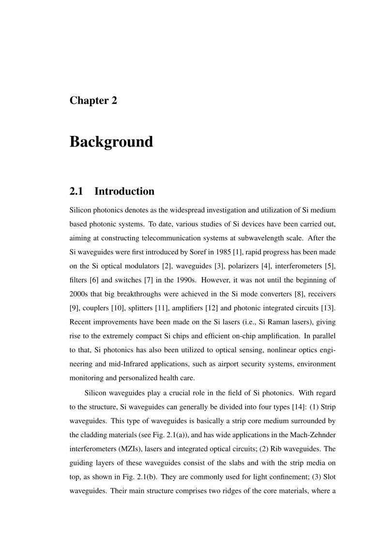
Silicon waveguides play a crucial role in the field of Si photonics. With regard
to the structure, Si waveguides can generally be divided into four types [14]: (1) Strip
waveguides. This type of waveguides is basically a strip core medium surrounded by
the cladding materials (see Fig. 2.1(a)), and has wide applications in the Mach-Zehnder
interferometers (MZIs), lasers and integrated optical circuits; (2) Rib waveguides. The
guiding layers of these waveguides consist of the slabs and with the strip media on
top, as shown in Fig. 2.1(b). They are commonly used for light confinement; (3) Slot
waveguides. Their main structure comprises two ridges of the core materials, where a
39
(a) (b)
(c) (d)
substrate
substrate
Si
Si
substrate
substrate
Si
Air
Si
Figure 2.1: Structure of four types of Si waveguides, including (a) a strip waveguide, (b) a ribwaveguide, (c) a slot waveguide and (d) a photonic crystal waveguide.
narrow gap exists in between, as illustrated in Fig. 2.1(c). Typically, these waveguides
are suitable for the mode field manipulation and optical sensing; (4) Photonic crystal
waveguides. They are usually photonic crystal structures containing a constant cross-
section region (shown in Fig. 2.1(d)), which allows the light propagation in specific
direction. One remarkable feature of this type of waveguides is the SL regimes, where
the device size and footprint can be easily downscaled. In this work, our main research
interest is in the strip and photonic crystal waveguides.
This chapter describes the background of this dissertation, which provides essen-
tial theoretical knowledge for the following chapters. Specifically, Sec. 2.2 introduces
the optical phenomena for the Si nanowire waveguides. Sec. 2.3 discusses important
linear and nonlinear optical parameters of strip and photonic crystal Si waveguides,
which occupies a fundamental part of this dissertation. Moreover, the schematics of the
investigated single- and multi-channel Si photonic systems are illustrated in Sec. 2.4.
Sec. 2.5 describes the basic types of optical signals used in this work. Next, the signal
propagation theory will be presented, which is one of the key aspects in the system
evaluation models. In particular, the full propagation theory that incorporates all the
essential optical effects in Si waveguides is presented in Sec. 2.6, whereas their lin-
earized version is outlined in Sec. 2.7. In the end, the computational algorithms of both
signal propagation models are discussed in Sec. 2.8.
40
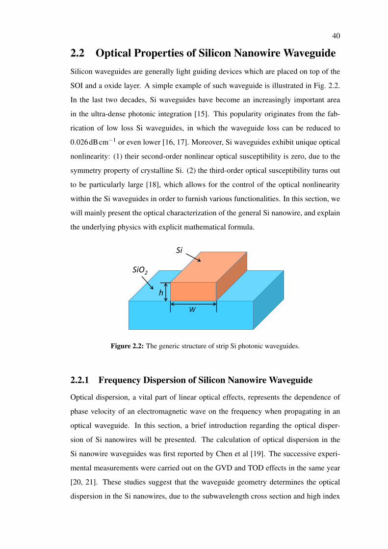
2.2 Optical Properties of Silicon Nanowire WaveguideSilicon waveguides are generally light guiding devices which are placed on top of the
SOI and a oxide layer. A simple example of such waveguide is illustrated in Fig. 2.2.
In the last two decades, Si waveguides have become an increasingly important area
in the ultra-dense photonic integration [15]. This popularity originates from the fab-
rication of low loss Si waveguides, in which the waveguide loss can be reduced to
0.026dBcm−1 or even lower [16, 17]. Moreover, Si waveguides exhibit unique optical
nonlinearity: (1) their second-order nonlinear optical susceptibility is zero, due to the
symmetry property of crystalline Si. (2) the third-order optical susceptibility turns out
to be particularly large [18], which allows for the control of the optical nonlinearity
within the Si waveguides in order to furnish various functionalities. In this section, we
will mainly present the optical characterization of the general Si nanowire, and explain
the underlying physics with explicit mathematical formula.
W
h
SiO2
Si
Figure 2.2: The generic structure of strip Si photonic waveguides.
2.2.1 Frequency Dispersion of Silicon Nanowire Waveguide
Optical dispersion, a vital part of linear optical effects, represents the dependence of
phase velocity of an electromagnetic wave on the frequency when propagating in an
optical waveguide. In this section, a brief introduction regarding the optical disper-
sion of Si nanowires will be presented. The calculation of optical dispersion in the
Si nanowire waveguides was first reported by Chen et al [19]. The successive experi-
mental measurements were carried out on the GVD and TOD effects in the same year
[20, 21]. These studies suggest that the waveguide geometry determines the optical
dispersion in the Si nanowires, due to the subwavelength cross section and high index
41
contrast. An analytic expression is used to describe the waveguide dispersion, by ex-
panding the mode propagation constant β (ω) in a Taylor series at the carrier frequency
ω0 [22, 23]:
β (ω) = n(ω)ω
c
= β0 +(ω−ω0)β1 +12!(ω−ω0)
2β2 +
13!(ω−ω0)
3β3 ++
14!(ω−ω0)
4β4...
(2.1)
where n(ω) is the refractive index, c is the speed of light, β0 ≡ β (ω0) is the propa-
gation constant at ω0, and βm =(
dmβ
dωm
)ω=ω0
represents the mth order dispersion co-
efficient. β1 is the inverse of the group velocity (vg = 1/β1), which is an important
parameter in the multi-wavelength signal co-propagation and several nonlinear phe-
nomena like FWM. β2 represents the GVD coefficient and determines the degree of
pulse broadening. Additionally, the GVD parameter D, with the mathematical defini-
tion of D= dβ1dλ
=−2πcλ 2 β2, is also widely used in the optical communications. β3 and β4
are useful parameters for optical pulses with femtosecond pulsewidth or even smaller.
To be more specific, the TOD effect would lead to the spectral asymmetry, whereas
the fourth dispersion effect has a significant contribution to the nonlinear frequency
mixing.
Dispersion engineering offers an effective approach to achieve the integration of
ultra-small optical devices on Si chips. Therefore, accurate theoretical description of
the dominant dispersive opticals effects (i.e., GVD and TOD) within Si nanowires is
indeed necessary to fulfill the goal mentioned above.
Group velocity dispersion means that each frequency component of optical signal
propagates at different speed, thus resulting in the optical pulse broadening. In par-
ticular, a zero-dispersion (ZGVD) wavelength λD usually exists in a Si nanowire [19],
which indicates a fact that no GVD effect occurs at λ = λD. The wavelength λD is of-
ten used to separate the normal dispersion (β2 > 0) and anomalous dispersion (β2 < 0)
regimes. Furthermore, the sign of β2 also influences the nonlinear optical effects in the
Si nanowires. A prominent example is the optical soliton, which is only generated in
anomalous dispersion regions. Additionally, the characteristic length of GVD is de-
noted as LD = τ2
|β2| (τ is the pulsewidth, unless otherwise is specified), which is used
42
to measure the minimum length where the GVD effect begins to strongly influence
the pulse evolution. Specifically, when the transmission distance is much larger than
LD (L LD), the GVD effect must be included in the theoretical description of pulse
dynamics.
Third-order dispersion effect can be easily observed when the optical pulse pos-
sesses the wavelength of λD, where no GVD occurs. As mentioned earlier, TOD can
also be important for optical signals with femtosecond pulsewidth or smaller. The TOD
effect is responsible for the pulse reshaping and distortion. Precisely, the positive (neg-
ative) value of β3 indicates that the oscillatory structure appears at the trailing (leading)
edge of the pulse. Similar to GVD, the characteristic length of TOD is denoted as
L′D = τ3
|β3| , indicating that the TOD affects the pulse propagation when L′D ≤ LD.
With respect to the calculation of these dispersion coefficients, the finite element
method (FEM) is applied on Eq. (2.1) in conjunction with the Sellmeier relation, which
for Si is written as [24]:
n(λ ) = ε +Aλ 2 +
Bλ 21
λ 2−λ 21, (2.2)
where λ1 = 1.1071µm, ε = 11.6858, A = 0.939816µm2, B = 8.10461×10⁻³.
2.2.2 Nonlinear Optical Properties of Silicon Nanowire Waveguide
Nonlinear optics represents a significant branch of the light-matter interactions, where
the waveguide response to the optical field behaves in a nonlinear manner. Various
optical effects are included in this field, namely the frequency-mixing process (e.g.,
second-harmonic generation, third-harmonic generation, and optical parametric gener-
ation), the optical Kerr effect (e.g., SPM and optical solitons), XPM, FWM, and the
Raman amplification [18]. In particular, the Si nanowires discussed in this dissertation
exhibit a strong anisotropic Kerr effect [25, 26], which is quantified by the third-order
susceptibility tensor χ(3) of Si. Due to the symmetry property of Si crystalline struc-
ture, two independent components, χ(3)1111 and χ
(3)1122, are selected to represent the 21
nonzero elements of χ(3). Moreover, χ(3) can be further simplified to one-component
independent variable, according to such relation, χ(3)1111/χ
(3)1122 = 2.36 [23, 25]. From
physical point of view, both the Kerr effect and TPA govern the third-order susceptibil-
ity in Si nanowires.
The nonlinear coefficient γ , a χ(3) related parameter, is introduced to determine
43
the waveguide nonlinearity:
γ =3ωΓ
4ε0Anlv2g, (2.3)
where Γ measures the effective nonlinear susceptibility, ω is the carrier frequency, Anl
is the cross sectional area of the Si waveguides, ε0 is the permittivity of free space,
and vg represents the GV [27]. Equation (2.3) shows that γ has strong dependence on
the operational frequency and the waveguide geometry. Different from silica fibers,
the nonlinear coefficient γ in Si nanowires is a complex number, which consists of
the real (γ ′) and imaginary (γ ′′) part. To be more specific, γ ′ corresponds to the SPM
effects [28] – the nonlinear response of the optical phase shift caused by the Kerr effect,
leading to optical spectral broadening. The corresponding nonlinear length is given by
LNL = 1/(γ ′P), where P is the power. γ ′′ quantifies the TPA effects [29], an optical
process describing the absorption of two photons in order to excite a molecule to a
higher energy state. Note also that TPA is a strong power-dependent phenomenon.
Further to that, possessing the SL spectral regions of the dispersive photonic-guiding
structures can increase the effective waveguide nonlinearity [30], since the nonlinearity
scales with vg as v−2g .
With regard to the multi-wavelength signal co-propagation in the same waveguide,
new nonlinear optical processes have to be taken into consideration, such as XPM [31],
multi-mode mixing, FWM and stimulated Raman scattering [23]. Among these effects,
only the XPM effect is added in the coupled-mode theory utilized in this dissertation.
XPM describes an optical process where the refractive index change is induced by one
pulse but probed by a second co-propagating pulse [32]. Therefore, two sets of stan-
dard nonlinear coefficients γi and γik are defined, in order to characterize the nonlinear
interaction between the co-propagating optical pulses [23]:
γi =3ωiΓi
4ε0Anlv2g,i, (2.4a)
γik =3ωiΓki
4ε0Anlvg,ivg,k, (2.4b)
γi and γik describe SPM and XPM interactions, respectively, with i or k the ith or kth
pulse during transmission channel. Γi is the effective nonlinear susceptibility for ωi,
while Γki measures the nonlinear susceptibility interaction between ωk and ωi. The
44
other relevant coefficients have been defined earlier in this section. More specific cases
regarding the nonlinear coefficients are discussed in Sec. 2.6.1 and Sec. 2.6.2.
2.2.3 Free Carrier Dynamics in Silicon Nanowire Waveguide
The carrier mechanism describes the interaction between FCs and the optical field in
Si nanowires, by means of including additional linear absorption and changing the
refractive index [33]. Apart from SPM, FCs make another contribution to the change
of refractive index. In general, the carrier density is a function of the time and distance.
The carrier relaxation time tc is a key parameter in the carrier dynamics, since FCs
can significantly influence signal reshaping when the signal pulsewith is larger than
tc. Thus, two relevant nonlinear effects are specified here, namely the FC absorption
(FCA) and FC-induced dispersion (FCD), with their mathematical formulas given by
[34]:
αFC =e3N
ε0cnω2
(1
µem∗2ce+
1µhm∗2ch
), (2.5a)
δnFC = − e2
2ε0nω2
(N
m∗ce+
N0.8
m∗ch
), (2.5b)
where δnFC characterizes the refractive index change induced by FCD, αFC stands
for the FCA coefficient, N is the FCs density, e is the electric charge of the electron,
m∗ce = 0.26 m0 and m∗ch = 0.39 m0 are the effective masses of the electron and the hole,
m0 is the mass of the electron, and µe(µh) is the electron (hole) mobility. Regarding
Eq. (2.5b), it is important to mention that this equation is only validated when N is
in unit of cm−3 [34]. Generally, the FCs relaxation time tc of Si nanowires is set to
be 0.5 ns [35]. Additional explanation for the evolution of FCs will be introduced in
Sec. 2.6.1 and Sec. 2.6.2.
2.3 Types of Silicon Photonic WaveguidesIn this section, we present two specific types of Si waveguides utilized throughout this
dissertation: The first waveguide is a single-mode Si photonic waveguide (Si-PhW)
with uniform cross-section, and buried in SiO2 cladding, as shown in Fig. 2.3(a). It
has a fixed height, h = 250nm, but tunable width, w, which offers the possibilities to
engineer the optical properties. From theoretical point of view, any dimensions of the
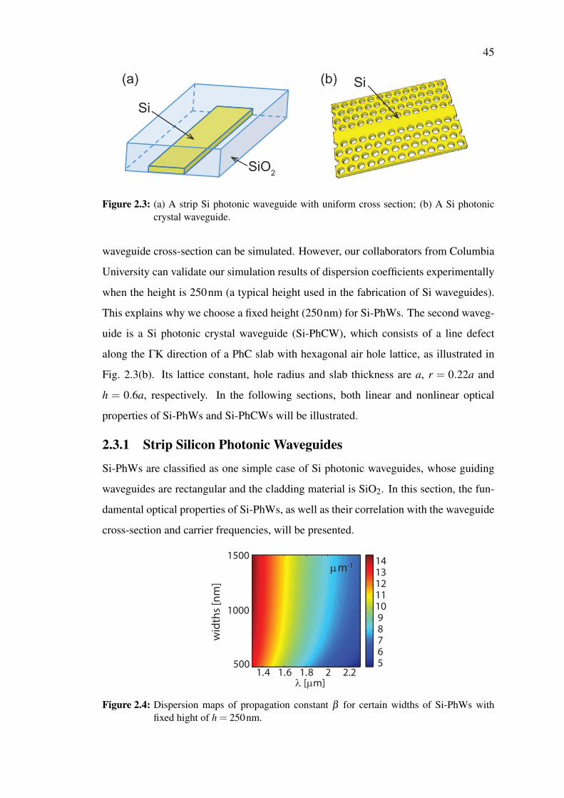
45
(a) (b)
Si
SiO2
Si
Figure 2.3: (a) A strip Si photonic waveguide with uniform cross section; (b) A Si photoniccrystal waveguide.
waveguide cross-section can be simulated. However, our collaborators from Columbia
University can validate our simulation results of dispersion coefficients experimentally
when the height is 250nm (a typical height used in the fabrication of Si waveguides).
This explains why we choose a fixed height (250nm) for Si-PhWs. The second waveg-
uide is a Si photonic crystal waveguide (Si-PhCW), which consists of a line defect
along the ΓK direction of a PhC slab with hexagonal air hole lattice, as illustrated in
Fig. 2.3(b). Its lattice constant, hole radius and slab thickness are a, r = 0.22a and
h = 0.6a, respectively. In the following sections, both linear and nonlinear optical
properties of Si-PhWs and Si-PhCWs will be illustrated.
2.3.1 Strip Silicon Photonic Waveguides
Si-PhWs are classified as one simple case of Si photonic waveguides, whose guiding
waveguides are rectangular and the cladding material is SiO2. In this section, the fun-
damental optical properties of Si-PhWs, as well as their correlation with the waveguide
cross-section and carrier frequencies, will be presented.
wid
ths
[nm
]
1.4 1.6 1.8 2 2.2500
1000
1500
56789
1011121314
λ [µm]
µm-1
Figure 2.4: Dispersion maps of propagation constant β for certain widths of Si-PhWs withfixed hight of h = 250nm.
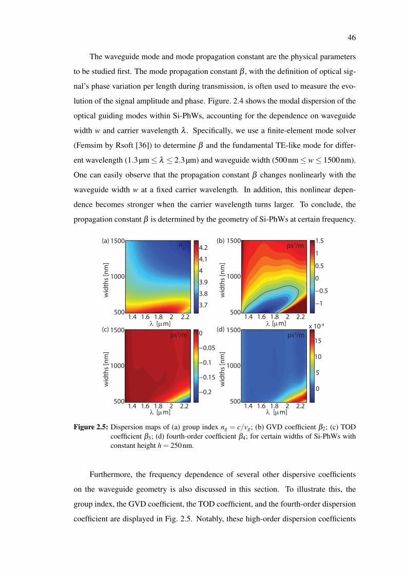
46
The waveguide mode and mode propagation constant are the physical parameters
to be studied first. The mode propagation constant β , with the definition of optical sig-
nal’s phase variation per length during transmission, is often used to measure the evo-
lution of the signal amplitude and phase. Figure. 2.4 shows the modal dispersion of the
optical guiding modes within Si-PhWs, accounting for the dependence on waveguide
width w and carrier wavelength λ . Specifically, we use a finite-element mode solver
(Femsim by Rsoft [36]) to determine β and the fundamental TE-like mode for differ-
ent wavelength (1.3µm≤ λ ≤ 2.3µm) and waveguide width (500nm≤ w≤ 1500nm).
One can easily observe that the propagation constant β changes nonlinearly with the
waveguide width w at a fixed carrier wavelength. In addition, this nonlinear depen-
dence becomes stronger when the carrier wavelength turns larger. To conclude, the
propagation constant β is determined by the geometry of Si-PhWs at certain frequency.
λ [µm]
wid
ths
[nm
]
1.4 1.6 1.8 2 2.2500
1000
1500
3.7
3.8
3.9
4
4.1
4.2ng
wid
ths
[nm
]
1.4 1.6 1.8 2 2.2500
1000
1500
−1
−0.5
0
0.5
1
1.5
λ [µm]
ps2/m
wid
ths
[nm
]
1.4 1.6 1.8 2 2.2500
1000
1500
−0.2
−0.15
−0.1
−0.05
0
λ [µm]
wid
ths
[nm
]
1.4 1.6 1.8 2 2.2500
1000
1500
0
5
10
15
x 10-4
λ [µm]
ps3/m ps4/m
(a) (b)
(c) (d)
Figure 2.5: Dispersion maps of (a) group index ng = c/vg; (b) GVD coefficient β2; (c) TODcoefficient β3; (d) fourth-order coefficient β4; for certain widths of Si-PhWs withconstant height h = 250nm.
Furthermore, the frequency dependence of several other dispersive coefficients
on the waveguide geometry is also discussed in this section. To illustrate this, the
group index, the GVD coefficient, the TOD coefficient, and the fourth-order dispersion
coefficient are displayed in Fig. 2.5. Notably, these high-order dispersion coefficients
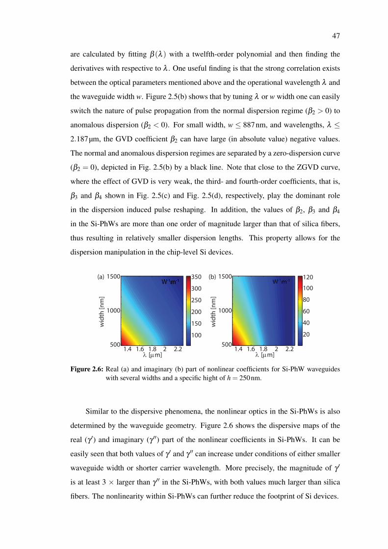
47
are calculated by fitting β (λ ) with a twelfth-order polynomial and then finding the
derivatives with respective to λ . One useful finding is that the strong correlation exists
between the optical parameters mentioned above and the operational wavelength λ and
the waveguide width w. Figure 2.5(b) shows that by tuning λ or w width one can easily
switch the nature of pulse propagation from the normal dispersion regime (β2 > 0) to
anomalous dispersion (β2 < 0). For small width, w ≤ 887nm, and wavelengths, λ ≤
2.187µm, the GVD coefficient β2 can have large (in absolute value) negative values.
The normal and anomalous dispersion regimes are separated by a zero-dispersion curve
(β2 = 0), depicted in Fig. 2.5(b) by a black line. Note that close to the ZGVD curve,
where the effect of GVD is very weak, the third- and fourth-order coefficients, that is,
β3 and β4 shown in Fig. 2.5(c) and Fig. 2.5(d), respectively, play the dominant role
in the dispersion induced pulse reshaping. In addition, the values of β2, β3 and β4
in the Si-PhWs are more than one order of magnitude larger than that of silica fibers,
thus resulting in relatively smaller dispersion lengths. This property allows for the
dispersion manipulation in the chip-level Si devices.
wid
th [n
m]
1.4 1.6 1.8 2 2.2500
1000
1500
100
150
200
250
300
350
λ [µm]
wid
th [n
m]
1.4 1.6 1.8 2 2.2500
1000
1500
20
40
60
80
100
120
λ [µm]
WWWWWWWW 1-1- mmmm-1-(a) (b)
Figure 2.6: Real (a) and imaginary (b) part of nonlinear coefficients for Si-PhW waveguideswith several widths and a specific hight of h = 250nm.
Similar to the dispersive phenomena, the nonlinear optics in the Si-PhWs is also
determined by the waveguide geometry. Figure 2.6 shows the dispersive maps of the
real (γ ′) and imaginary (γ ′′) part of the nonlinear coefficients in Si-PhWs. It can be
easily seen that both values of γ ′ and γ ′′ can increase under conditions of either smaller
waveguide width or shorter carrier wavelength. More precisely, the magnitude of γ ′
is at least 3 × larger than γ ′′ in the Si-PhWs, with both values much larger than silica
fibers. The nonlinearity within Si-PhWs can further reduce the footprint of Si devices.
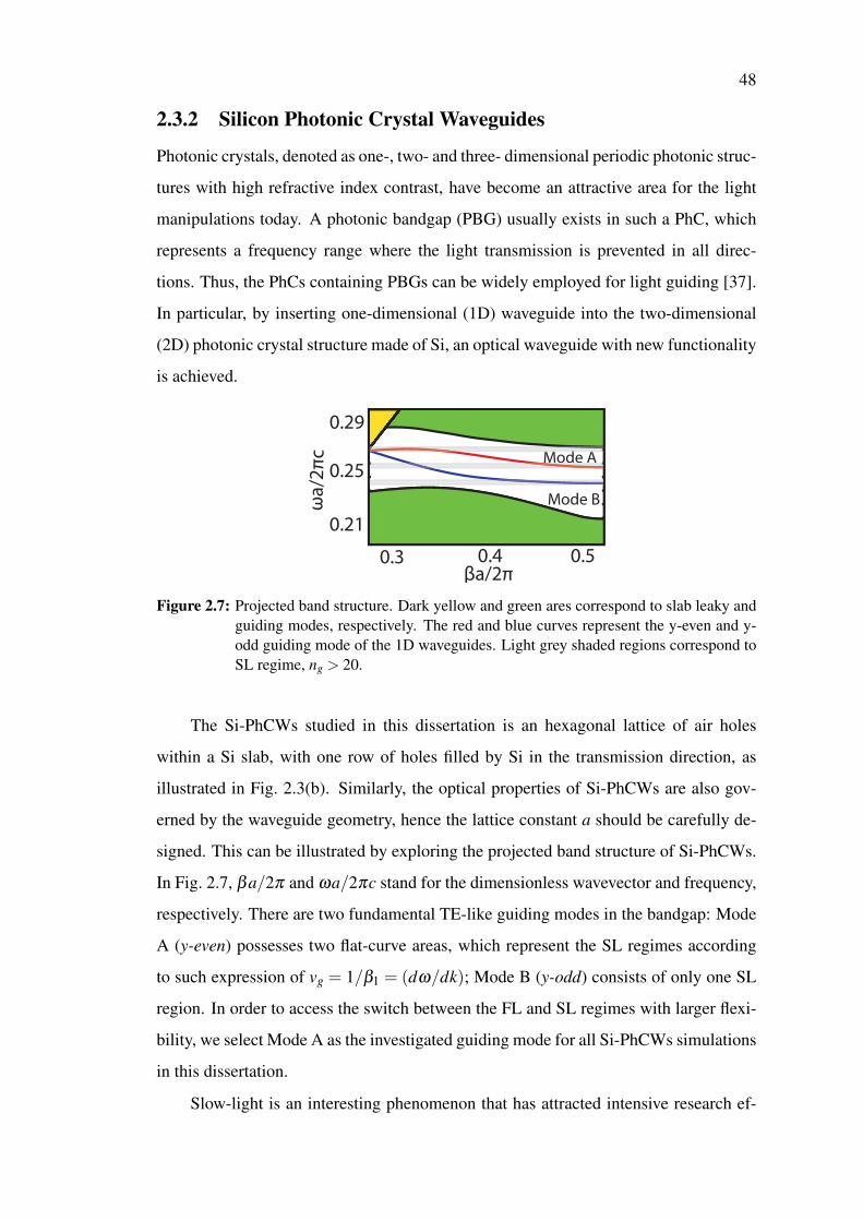
48
2.3.2 Silicon Photonic Crystal Waveguides
Photonic crystals, denoted as one-, two- and three- dimensional periodic photonic struc-
tures with high refractive index contrast, have become an attractive area for the light
manipulations today. A photonic bandgap (PBG) usually exists in such a PhC, which
represents a frequency range where the light transmission is prevented in all direc-
tions. Thus, the PhCs containing PBGs can be widely employed for light guiding [37].
In particular, by inserting one-dimensional (1D) waveguide into the two-dimensional
(2D) photonic crystal structure made of Si, an optical waveguide with new functionality
is achieved.
0.29
0.25
0.21
ωa/
2πc
0.3 0.4 0.5βa/2π
Mode B
Mode AodM d A
Figure 2.7: Projected band structure. Dark yellow and green ares correspond to slab leaky andguiding modes, respectively. The red and blue curves represent the y-even and y-odd guiding mode of the 1D waveguides. Light grey shaded regions correspond toSL regime, ng > 20.
The Si-PhCWs studied in this dissertation is an hexagonal lattice of air holes
within a Si slab, with one row of holes filled by Si in the transmission direction, as
illustrated in Fig. 2.3(b). Similarly, the optical properties of Si-PhCWs are also gov-
erned by the waveguide geometry, hence the lattice constant a should be carefully de-
signed. This can be illustrated by exploring the projected band structure of Si-PhCWs.
In Fig. 2.7, βa/2π and ωa/2πc stand for the dimensionless wavevector and frequency,
respectively. There are two fundamental TE-like guiding modes in the bandgap: Mode
A (y-even) possesses two flat-curve areas, which represent the SL regimes according
to such expression of vg = 1/β1 = (dω/dk); Mode B (y-odd) consists of only one SL
region. In order to access the switch between the FL and SL regimes with larger flexi-
bility, we select Mode A as the investigated guiding mode for all Si-PhCWs simulations
in this dissertation.
Slow-light is an interesting phenomenon that has attracted intensive research ef-
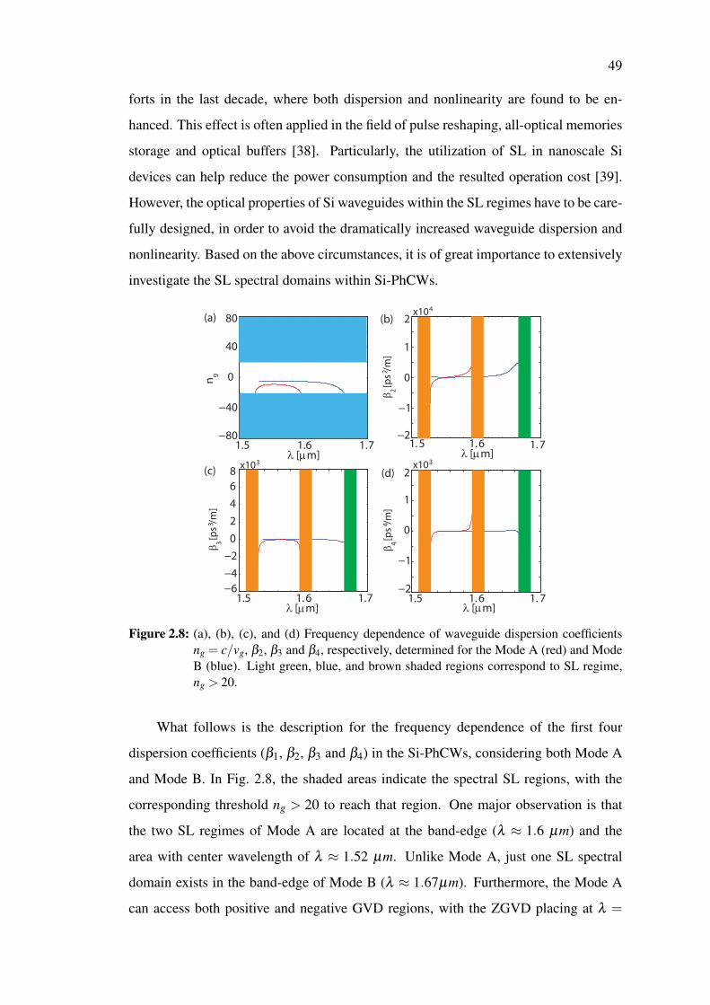
49
forts in the last decade, where both dispersion and nonlinearity are found to be en-
hanced. This effect is often applied in the field of pulse reshaping, all-optical memories
storage and optical buffers [38]. Particularly, the utilization of SL in nanoscale Si
devices can help reduce the power consumption and the resulted operation cost [39].
However, the optical properties of Si waveguides within the SL regimes have to be care-
fully designed, in order to avoid the dramatically increased waveguide dispersion and
nonlinearity. Based on the above circumstances, it is of great importance to extensively
investigate the SL spectral domains within Si-PhCWs.
1.5 1.6 1.7−80
−40
0
40
80
n g
λ [µm]1. 5 1. 6 1. 7
−2
−1
0
1
2
β 2 [ps2 /m
]
x104
λ [µm]
1.5 1. 6 1.7−6−4−2
02468
β 3 [ps3 /m
]
x103
λ [µm]1.5 1. 6 1. 7
−2
−1
0
1
2x10³
β 4 [ps4 /m
]
λ [µm]
(a) (b)
(c) (d)
Figure 2.8: (a), (b), (c), and (d) Frequency dependence of waveguide dispersion coefficientsng = c/vg, β2, β3 and β4, respectively, determined for the Mode A (red) and ModeB (blue). Light green, blue, and brown shaded regions correspond to SL regime,ng > 20.
What follows is the description for the frequency dependence of the first four
dispersion coefficients (β1, β2, β3 and β4) in the Si-PhCWs, considering both Mode A
and Mode B. In Fig. 2.8, the shaded areas indicate the spectral SL regions, with the
corresponding threshold ng > 20 to reach that region. One major observation is that
the two SL regimes of Mode A are located at the band-edge (λ ≈ 1.6 µm) and the
area with center wavelength of λ ≈ 1.52 µm. Unlike Mode A, just one SL spectral
domain exists in the band-edge of Mode B (λ ≈ 1.67µm). Furthermore, the Mode A
can access both positive and negative GVD regions, with the ZGVD placing at λ =
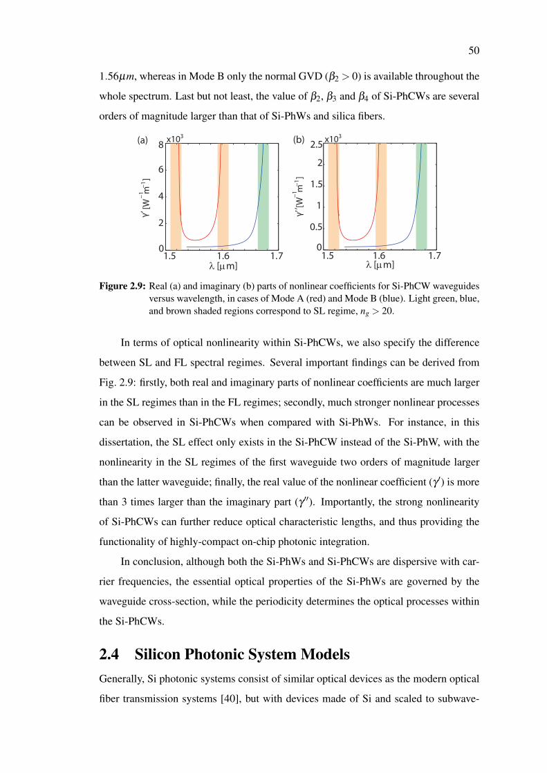
50
1.56µm, whereas in Mode B only the normal GVD (β2 > 0) is available throughout the
whole spectrum. Last but not least, the value of β2, β3 and β4 of Si-PhCWs are several
orders of magnitude larger than that of Si-PhWs and silica fibers.
1.5 1.6 1.70
2
4
6
8 [
W−1
m−1
]γ’
x103
λ [µm]1.5 1.6 1.7
0
0.5
1
1.5
2
2.5 x10³
[W
−1m
−1]
γ’’
λ [µm]
(a) (b)
Figure 2.9: Real (a) and imaginary (b) parts of nonlinear coefficients for Si-PhCW waveguidesversus wavelength, in cases of Mode A (red) and Mode B (blue). Light green, blue,and brown shaded regions correspond to SL regime, ng > 20.
In terms of optical nonlinearity within Si-PhCWs, we also specify the difference
between SL and FL spectral regimes. Several important findings can be derived from
Fig. 2.9: firstly, both real and imaginary parts of nonlinear coefficients are much larger
in the SL regimes than in the FL regimes; secondly, much stronger nonlinear processes
can be observed in Si-PhCWs when compared with Si-PhWs. For instance, in this
dissertation, the SL effect only exists in the Si-PhCW instead of the Si-PhW, with the
nonlinearity in the SL regimes of the first waveguide two orders of magnitude larger
than the latter waveguide; finally, the real value of the nonlinear coefficient (γ ′) is more
than 3 times larger than the imaginary part (γ ′′). Importantly, the strong nonlinearity
of Si-PhCWs can further reduce optical characteristic lengths, and thus providing the
functionality of highly-compact on-chip photonic integration.
In conclusion, although both the Si-PhWs and Si-PhCWs are dispersive with car-
rier frequencies, the essential optical properties of the Si-PhWs are governed by the
waveguide cross-section, while the periodicity determines the optical processes within
the Si-PhCWs.
2.4 Silicon Photonic System ModelsGenerally, Si photonic systems consist of similar optical devices as the modern optical
fiber transmission systems [40], but with devices made of Si and scaled to subwave-
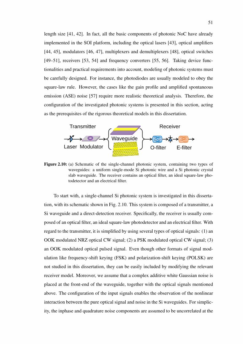
51
length size [41, 42]. In fact, all the basic components of photonic NoC have already
implemented in the SOI platform, including the optical lasers [43], optical amplifiers
[44, 45], modulators [46, 47], multiplexers and demultiplexers [48], optical switches
[49–51], receivers [53, 54] and frequency converters [55, 56]. Taking device func-
tionalities and practical requirements into account, modeling of photonic systems must
be carefully designed. For instance, the photodiodes are usually modeled to obey the
square-law rule. However, the cases like the gain profile and amplified spontaneous
emission (ASE) noise [57] require more realistic theoretical analysis. Therefore, the
configuration of the investigated photonic systems is presented in this section, acting
as the prerequisites of the rigorous theoretical models in this dissertation.
ModulatorLaser
Waveguide
O-filter E-filter
Transmitter Receiver
Figure 2.10: (a) Schematic of the single-channel photonic system, containing two types ofwaveguides: a uniform single-mode Si photonic wire and a Si photonic crystalslab waveguide. The receiver contains an optical filter, an ideal square-law pho-todetector and an electrical filter.
To start with, a single-channel Si photonic system is investigated in this disserta-
tion, with its schematic shown in Fig. 2.10. This system is composed of a transmitter, a
Si waveguide and a direct-detection receiver. Specifically, the receiver is usually com-
posed of an optical filter, an ideal square-law photodetector and an electrical filter. With
regard to the transmitter, it is simplified by using several types of optical signals: (1) an
OOK modulated NRZ optical CW signal; (2) a PSK modulated optical CW signal; (3)
an OOK modulated optical pulsed signal. Even though other formats of signal mod-
ulation like frequency-shift keying (FSK) and polarization-shift keying (POLSK) are
not studied in this dissertation, they can be easily included by modifying the relevant
receiver model. Moreover, we assume that a complex additive white Gaussian noise is
placed at the front-end of the waveguide, together with the optical signals mentioned
above. The configuration of the input signals enables the observation of the nonlinear
interaction between the pure optical signal and noise in the Si waveguides. For simplic-
ity, the inphase and quadrature noise components are assumed to be uncorrelated at the
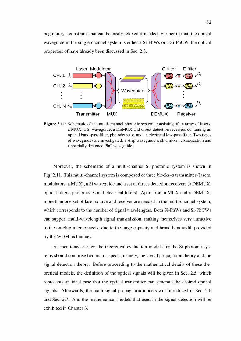
52
beginning, a constraint that can be easily relaxed if needed. Further to that, the optical
waveguide in the single-channel system is either a Si-PhWs or a Si-PhCW, the optical
properties of have already been discussed in Sec. 2.3.
Laser
DEMUX Receiver
…
CH. 1
CH. 2
CH. N
1
2
N
…
1D
2D
ND
…
O-filter E-filter Modulator
MUX
Waveguide
Transmitter
Figure 2.11: Schematic of the multi-channel photonic system, consisting of an array of lasers,a MUX, a Si waveguide, a DEMUX and direct-detection receivers containing anoptical band-pass filter, photodetector, and an electrical low-pass filter. Two typesof waveguides are investigated: a strip waveguide with uniform cross-section anda specially designed PhC waveguide.
Moreover, the schematic of a multi-channel Si photonic system is shown in
Fig. 2.11. This multi-channel system is composed of three blocks–a transmitter (lasers,
modulators, a MUX), a Si waveguide and a set of direct-detection receivers (a DEMUX,
optical filters, photodiodes and electrical filters). Apart from a MUX and a DEMUX,
more than one set of laser source and receiver are needed in the multi-channel system,
which corresponds to the number of signal wavelengths. Both Si-PhWs and Si-PhCWs
can support multi-wavelength signal transmission, making themselves very attractive
to the on-chip interconnects, due to the large capacity and broad bandwidth provided
by the WDM techniques.
As mentioned earlier, the theoretical evaluation models for the Si photonic sys-
tems should comprise two main aspects, namely, the signal propagation theory and the
signal detection theory. Before proceeding to the mathematical details of these the-
oretical models, the definition of the optical signals will be given in Sec. 2.5, which
represents an ideal case that the optical transmitter can generate the desired optical
signals. Afterwards, the main signal propagation models will introduced in Sec. 2.6
and Sec. 2.7. And the mathematical models that used in the signal detection will be
exhibited in Chapter 3.
53
2.5 Optical Signal Modulation FormatsThe demand to construct the broadband and high-capacity information networks is
ever-increasing each year. Some technologies are hopeful to satisfy and maintain such
great demand, such as the WDM technology. Apart from the improvement on the de-
vice layer, the utilization of advanced optical processing techniques is also viewed as a
efficient solution [58]. In particular, advanced optical modulation formats have been in-
tensively investigated over the recent years [59], as they can potentially become viable
alternatives to more commonly used OOK modulation. In the context of optical fiber
communications it has become clear that, among the advanced modulation formats
of optical signals, PSK modulation provides unique advantages, including increased
spectral efficiency, superior tolerance to chromatic dispersion and polarization-mode
dispersion, and less stringent bandwidth requirements [60, 61]. Moreover, higher spec-
tral efficiency can be achieved by employing PSK modulation schemes with increased
complexity, such as quadrature PSK (4PSK) and 8-ary PSK (8PSK) modulation for-
mats, or by combining amplitude-shift keying (ASK) and PSK formats, which we call
here ASK-PSK modulation schemes. Importantly, whereas high-order modulation for-
mats have been studied extensively in the context of optical fiber and other commu-
nication systems [59, 62, 63], currently a similar theoretical analysis addressing the
performance of such modulation schemes when used in photonics systems containing
silicon based optical communication links is not available.
Several types of optical signals are introduced in this section, including the OOK
modulated CW signals (uOOK), the PSK modulated CW signals (uPSK) and the OOK
modulated Gaussian pulsed signals (uG), in presence of the complex white gaussian
noise. Therefore, their explicit expressions for a given bit are illustrated below:
uOOK(z, t) = [√
P(z)+a(z, t)]e− jΦ(z), (2.6a)
uPSK(z, t) = [√
P(z)e jΦ0 +a(z, t)]e− jΦ(z), (2.6b)
uG(z, t) = [√
P(z)e−t2/2T 20 +a(z, t)]e− jΦ(z), (2.6c)
Here, P represents the peak power of input signal, a is the complex white noise, Φ(z)
stands for the general phase, T0 is the pulsewidth, and Φ0 is defined by the PSK signal
modulation formats. In particular, Φ(z) is set to 0 (in unit of rad) when at z = 0. It
54
is important to stress that in our model the pure signal and white noise have different
phase. This is so because the noise function, a(z, t), is complex-valued and therefore
an additional phase is introduced. As for the ASK-PSK modulation, there would be
at least two different power levels involved. More details about the PSK modulation
formats will be discussed in Sec. 7.3.
2.6 Theory of Optical Signal Propagation in Silicon
Waveguides
Instrumental insights into the optical properties of both Si-PhWs and Si-PhCWs can be
obtained by analyzing the evolution of the optical field and FCs in the Si waveguides.
Thus, the theory of signal propagation will be presented in this section. Different from
the pulse propagation model for silica fibers, the nonlinear optical susceptibilities of
Si-PhWs and Si-PhCWs are mathematically described as tensors instead of scalars.
Moreover, the FCs dynamcis is included in the case of Si waveguides, but not silica
fibers. Generally, this signal propagation model designed for Si waveguides is based on
a NLSE describing the optical pulse propagation and a rate equation for FCs [64, 66].
Moreover, the SSFM and a fifth-order Runge-Kutta method are applied in order to de-
rive semi-analytical solutions with regard to the coupled equations mentioned above,
with their numerical implementation described in Sec. 2.8.1. Both single- and multi-
wavelength pulse propagation will be considered in this dissertation, with the corre-
sponding mathematical models described in Sec. 2.6.1 and Sec. 2.6.2, respectively.
2.6.1 Theory of Single-wavelength Optical Signal Propagation
The strategy for simplifying the evolution of the optical field in Si waveguides, is to
divide the waveguide into an unperturbed part and a perturbed part. In particular, the
nonlinear effects (SPM, TPA) and the change of the dielectric constant act as the in-
fluence sources for the electromagnetic field propagation in the perturbed waveguides
[23]. Therefore, we start the mathematical description with the Lorentz reciprocity
theorem [67]:∂
∂ z
∫A∞
F · ezdA =∫
A∞
∇ ·FdA, (2.7)
55
where the vector field F is defined blow:
F = EL∗×HNL +ENL×HL
∗, (2.8)
Here, two sets of variables are defined as follows: (EL,HL) = (E0,H0) is the guid-
ing mode in the unperturbed waveguides, whereas (ENL,HNL) = (E,H) represents the
mode for the perturbed waveguide. By combining with the source-free Maxwell equa-
tions, Eq. (2.7) can cast in the following:
∂
∂ z
∫A∞
(EL∗×HNL +ENL×HL
∗) · ezdA = iω∫
A∞
δP ·ELdA (2.9)
where δP is the total mode polarization, which contains a linear and a nonlinear ele-
ment, namely δP = δεE = δPL+δPNL. To be more specific, δPL stands for the change
of dielectric constant, according to δPL = δεLE. Here, the parameter δεL is defined be-
low:
δεL(ω) =iε0cnαin
ω+2ε0nδnFC +
iε0cnαFC
ω, (2.10)
where ε0 is the vacuum permittivity and αin is the intrinsic loss coefficient. δnFC and
αFC represent the FC-induced change in refractive index and FCA coefficient, respec-
tively, with their mathematical definition given by Eq. (2.5b) and Eq. (2.5a). Further-
more, the nonlinear polarization δPNL is described by the formula below:
δPNL(ω) =34
ε0χ3(ω;ω,−ω,ω)
...E(ω)E∗(ω)E(ω), (2.11)
where χ3(ω;ω,−ω,ω) is the third-order susceptibility coefficient. The second step is
to extract the explicit expression for the perturbed electromagnetic fields. The unper-
turbed fields (E0,H0) are defined below, with the total power P0:
E0 =12
√Z0P0
A0e(rt ,ω0)ei(β0z−ω0t), (2.12a)
H0 =12
√P0
Z0A0h(rt ,ω0)ei(β0z−ω0t), (2.12b)
56
where Z0 =√
µ0/ε0, e(rt) and h(rt) are the electromagnetic fields in the xy plane.
Normalization is then performed on e and h in our mathematical analysis,
14A0
∫∞
(e×h∗+ e∗×h) · ezdA = 1. (2.13)
For convenience, a slowly varying normalized complex envelope u(z,ω) is defined,
whose input peak amplitude equals to 1 in the time domain. Therefore, in the perturbed
part, the electromagnetic field (E,H) with total power of P0|u(z,ω)|2 are obtained:
E =12
√Z0P0
A0u(z,ω)e(rt ,ω)ei(β z−ωt), (2.14a)
H =12
√P0
Z0A0u(z,ω)h(rt ,ω)ei(β z−ωt), (2.14b)
Finally, we can derive the perturbed NLSE for normalized amplitude u(z, t) by com-
bining Eqs. (2.9), (2.10), (2.12), (2.13), (2.14)and performing the Fourier Transform
on the resulting equation from the frequency domain to the time-domain:
j(
∂u∂ z
+1vg
∂u∂ t
)− β2
2∂ 2u∂ t2 −
jβ3
6∂
3u∂ t3 =− jcκ
2nvg(αin +αFC)u−
ω0κ
nvgδnFCu− γ|u|2u,
(2.15)
The terms in Eq. (2.15) describe well known linear and nonlinear optical effects.
Specifically, the second and third terms on the left-side describe the GVD and TOD, re-
spectively. Notably, the dispersion coefficients, β1 = 1/vg, β2 and β3 are derived from
Eq. (2.1) at the carrier frequency of ω0. Moreover, from the right-side of Eq. (2.15),
the first term corresponds to the intrinsic waveguide loss and FCA, the second term
describes the FCD, whereas the last term represents nonlinear effects, namely the SPM
and TPA. In terms of the nonlinear parameters, the structures of the Si waveguides need
to be taken into account. Particularly, the nonlinearity in the Si-PhWs is determined by
their cross-section, while for Si-PhCWs the lattice constant a is the dominant factor.
The corresponding nonlinear coefficients are given by:
γ =3ωε0
16v2g
Γ
W 2 , (2.16a)
57
γ =3ωε0a16v2
g
Γ
W 2 , (2.16b)
Here and in what follows of this chapter, bar and tilde symbols represent that the phys-
ical quantities refer to Si-PhWs and Si-PhCWs, respectively, unless otherwise is speci-
fied. W and W are the optical mode energy per unit length of Si-PhW and optical mode
energy contained in a unit cell of Si-PhCW, with the expression listed below:
W =14
∫S
[ε(r)|e(r,ω)|2 +µ0|h(r,ω)|2
]dS, (2.17a)
W =14
∫Vcell
[ε(r)|e(r,ω)|2 +µ0|h(r,ω)|2
]dV. (2.17b)
As mentioned earlier, e(r,ω) and h(r,ω) are the electric and magnetic field respec-
tively. S and Vcell are the cross-section area of Si-PhWs and the unit cell volume of
Si-PhCWs, correspondingly. Furthermore, the coefficients Γ and Γ are the mode medi-
ated nonlinear susceptibility for the Si-PhWs and Si-PhCWs, respectively:
Γ =∫
Snl
e∗(r) · χ(3)(ω,−ω,ω)...e(r)e∗(r)e(r)dS, (2.18a)
Γ =∫
Vnl
e∗(r) · χ(3)(ω,−ω,ω)...e(r)e∗(r)e(r)dV, (2.18b)
In order to facilitate a comparison between the optical properties of Si-PhWs and Si-
PhCWs, we recast Eqs. (2.3) in a new form of Eqs. (2.16). Furthermore, κ and κ
measure the overlap integral between the active area of Si-PhWs and Si-PhCWs and
the optical mode, whose mathematical formulae are expressed as:
κ =n2 ∫
A0|e(rt)|2dA∫
A∞n2(rt)|e(rt)|2dA
, (2.19a)
κ =an2 ∫
A0|e(r)|2dA∫
VCelln2(rt)|e(r)|2dV
, (2.19b)
Equations. (2.19) suggest that only a fraction of the power from the electromagnetic
mode affects the FCs generation, since the mode profile only partially overlaps with Si
waveguides.
A modified rate equation is used to describe the carrier dynamics during the trans-
58
mission in Si waveguides:
∂N∂ t
=−Nτc
+γ′′
hω0Anl|u|4, (2.20)
where N represents the FCs density, τc is the FC relaxation time, and Anl is the effective
mode area. We use Anl = wh (Anl = ah) for the Si-PhW (Si-PhCW) systems, although
more accurate formulae for Anl exist [23, 64, 65, 68]. Since we consider high-index
contrast systems, the optical field is strongly confined in the waveguide, so that using
the geometrical area for Anl is a reasonable approximation. Here and in what follows
ζ ′ (ζ ′′) represents the real (imaginary) part of the complex number, ζ . In conclusion,
both Eq. (2.15) and Eq. (2.20) are described to describe the single-wavelength pulse
propagation.
2.6.2 Theory of Multi-wavelength Optical Signal Propagation
As an expansion of the single-wavelength propagation model, the multi-wavelength
propagation model will be presented in this section to fully capture the evolution of
multi-wavelength optical fields in coupled with FCs. Note that the FWM terms are not
included in our multi-wavelength propagation model, since the phase-match condition
is not satisfied with the values of wavelength used in this dissertation. Thus, the multi-
wavelength model can be derived by adding the XPM term in Eqs. (2.15) and (2.20)
[19, 64, 68]:
j∂ui
∂ z+ j(
1vg,i− 1
vg,ref
)∂ui
∂T−
β2,i
2∂ 2ui
∂T 2 =−ωiκi
nvg,iδnFCui−
jcκi
2nvg,i(αin +αFC)ui
−(
γi|ui|2 +2 ∑k 6=i
γik|uk|2)
ui, (2.21a)
∂N∂ t
=−Nτc
+∑i,k
Cik|ui|2|uk|2, (2.21b)
Here, i and k indicate the transmission channel index with the carrier frequency ωi and
ωk, and the channel index ranges from 1 to M (M is the total number of channels).
ui(z,T ) is the ith pulse envelope, measured in√
W, z and T are the distance along the
Si waveguide and time in a reference system moving with velocity vg,ref, respectively.
Specifically, T = t− z/vg,ref, where t is the physical time. The definitions of vg,i, β2,i,
κi, δnfc, αfc, αin, γi and τc can be found in Sec. 2.6.1, with the central frequency to be
59
ωi this time. γik is the nonlinear coefficient corresponding to the XPM effect in the Si
waveguide. For completeness, we present not only the mathematical formula for the γik
within Si-PhWs and Si-PhCWs, but also for γi:
γi =3ωiε0
16v2g,i
Γi
W 2i, γik =
3ωiε0
16vg,ivg,k
Γik
WiWk, (2.22a)
γi =3ωiε0a16v2
g,i
Γi
W 2i, γik =
3ωiε0a16vg,ivg,k
Γik
WiWk. (2.22b)
The optical mode energy per unit length (Wi) and per unit cell (Wi) at ωi have been
given by Eqs. (2.5). Additionally, the nonlinear susceptibility coefficients, Γi and Γi j,
are defined below:
Γi =∫
Snl
e∗i (r) · χ(3)(ωi,−ωi,ωi)...ei(r)e
∗i (r)ei(r)dS, (2.23a)
Γik =∫
Snl
e∗i (r) · χ(3)(ωk,−ωk,ωi)...ek(r)e
∗k(r)ei(r)dS, (2.23b)
Γi =∫
Vnl
e∗i (r) · χ(3)(ωi,−ωi,ωi)...ei(r)e
∗i (r)ei(r)dV, (2.23c)
Γik =∫
Vnl
e∗i (r) · χ(3)(ωk,−ωk,ωi)...ek(r)e
∗k(r)ei(r)dV, (2.23d)
With regard to the carrier dynamics in the multi-wavelength propagation, we use
the coefficient Cik in Eq. (2.21b) to quantify the rate at which the optical energy is
transferred to FCs. And this important parameter, Cik, is denoted as:
Cik =
γ′′i
hωiAnl, i = k,
4γ′′ik
h(ωi +ωk)Anl, i 6= k.
(2.24)
The explicit description of the effective mode area Anl has been given in the last para-
graph of Sec. 2.6.1. More rigorous definitions related to the multi-wavelength propa-
gation can be found in refs. [68, 69].
2.7 Linearized Theoretical Model for CW Noise Dy-
namicsThe linearized models for CW signal propagation in Si waveguides are presented in this
section. Similar to the propagation theory introduced in Sec. 2.6, both linearized mod-
60
els regarding single- and multi-wavelength propagation will be introduced in Sec. 2.7.1
and Sec. 2.7.2, respectively. These models assume that the nonlinear noise-noise in-
teraction during transmission can be negligible [70, 71], due to the fact that the power
of noise at the input of waveguides is much smaller than that of optical signal. Thus,
two resulting approximations are proposed: firstly, all quadratic and higher-order noise
terms are neglected; secondly, δnFC is proportional to carrier density N. Particularly,
a numerical ODE solver is employed in the linearized propagation models, in order to
reduce the computational time and maintain the simulation reliability, which will be
introduced in Sec. 2.8.2.
2.7.1 Single-channel CW Noise Linearization
In single-channel Si waveguides, both an OOK modulated CW signal (uOOK) and a PSK
modulated CW signal (uPSK) will be thoroughly studied [72, 73]. After comparing the
definition of these two signals via Eq. (2.6a) and Eq. (2.6b), one can tell that PSK
signals contain an extra term of Φ0, which increases the complexity of the linearized
propagation model. However, uOOK can be written in the form of uPSK by setting Φ0 =
0 in Eq. (2.6b). Therefore, one common linearized propagation model is proposed in
this section, which is capable of describing the evolution of these two types of CW
signals in the single-channel Si waveguides.
Firstly, the FCs dynamics (Eq. (2.20)) is considered in the stationary regime,∂N∂ t = 0. Then, the steady state FCs density, Ns, is obtained:
Ns(z) =tcγ′′
hω0AnlP2(z)≡ ξ P2(z). (2.25)
A self-consistency condition for the validity of our model is that the FC induced disper-
sion is small, namely δnfc . 10−3. In addition, stationary regime can be reached only if
the bit window is much smaller than the FC relaxation time, a condition satisfied in all
our numerical simulations. This serves as one of the necessary conditions to construct
the linearized propagation models. In the small noise limit, Eq. (2.15) can be linearized
and transformed to a system of ODEs, which is much less demanding computationally.
The next step is to substitute Eq. (2.6b) into Eq. (2.15), and discard all quadratic
and higher-order terms of a(z, t) in the resulted equation. Notably, the TOD and fourth-
61
order dispersion terms will not be included in the linearized models, since their effects
are negligible for pulse widths of picoseconds and larger when compared with the GVD
effect. Then, in conjunction with Eq. (2.25), we arrive to the following system of
equations for uOOK and uPSK:
dPdz
=− cκ
nvgαinP− cκ
nvgσαξ P3−2γ
′′P2, (2.26a)
dΦ
dz=− ω0κ
nvgσnξ P2− γ
′P, (2.26b)
∂a∂ z
=− jβ2
2∂ 2a∂ t2 −
cκ
2nvgαina− γ
′′Pa+ j2γPe jΦ0(cosΦ0a′+ sinΦ0a′′)
− cκ
2nvgσαξ P2[a+4e jΦ0(cosΦ0a′+ sinΦ0a′′)]
+ j4ω0κ
nvgσnξ P2e jΦ0(cosΦ0a′+ sinΦ0a′′). (2.26c)
Here, σn and σα quantify the influence of FCs on the linear optical properties of silicon
via δnfc = σnN and αfc = σαN, and have values of σα = 1.45×10⁻²¹(λ/λ0)2 (in units
of m2) and σn =σ(λ/λ0)2 (in units of m3), with σ being a power-dependent coefficient
[74] and λ0 = 1550nm is a reference wavelength. Here and in what follows a′(z, t) and
a′′(z, t) represent the real and imaginary parts of the noise a(z, t), respectively. It can
be seen from Eqs. (2.26) that the optical power P can be calculated independently of
other signal parameters and, as expected, it decays due to intrinsic losses, FC absorption
(FCA), and two-photon absorption (TPA). On the other hand, the variation of the global
phase, Φ, is determined by the FC dispersion (FCD) and self-phase modulation (SPM)
effects. Importantly, the initial phase Φ0 of PSK modulation formats does not affect the
evolution of the signal power and global phase, thus allowing uOOK and uPSK to share
the same mathematical formulation for these two physical quantities.
In order to simplify the noise calculations, we transform Eq. (2.26c) to a system
of ODEs. For this, we combine this equation with its complex conjugate and Fourier
transform the resulting equations for the in-phase and quadrature noise components,
a′(z, t) and a′′(z, t), respectively. These calculations yield:
dA′
dz=− β2
2Ω
2A′′− cκ
2nvgαiA′−
cκ
2nvgσαξ P2[A′+4cosΦ0(cosΦ0A′+ sinΦ0A′′)]
− 4ω0κ
nvgσnξ P2 sinΦ0(cosΦ0A′+ sinΦ0A′′)− γ
′′PA′
62
−2(γ ′ sinΦ0 + γ′′ cosΦ0)P(cosΦ0A′+ sinΦ0A′′), (2.27a)
dA′′
dz=
β2
2Ω
2A′− cκ
2nvgαiA′′−
cκ
2nvgσαξ P2[A′′+4sinΦ0(cosΦ0A′+ sinΦ0A′′)]
+4ω0κ
nvgσnξ P2 cosΦ0(cosΦ0A′+ sinΦ0A′′)− γ
′′PA′′
+2(γ ′ cosΦ0− γ′′ sinΦ0)P(cosΦ0A′+ sinΦ0A′′). (2.27b)
where Ω = ω −ω0 and A′(z,Ω) = Fa′(z, t) and A′′(z,Ω) = Fa′′(z, t) are the
Fourier transforms of the two noise components. Furthermore, a detailed comparison
between the full propagation model and its linearized version was carried out for the
single-channel systems in Chapter 5, the conclusion being that for practical values of
the system parameters the linearized model is accurate.
To this end, both the full propagation model and its linearized version have been
derived for the single-channel optical system. In addition, these models can be easily
extended to other types of optical waveguides or more complicated optical devices.
2.7.2 Multi-channel CW Noise Linearization
In this section, the linearized approach for multi-wavelength propagation are presented,
considering only the OOK CW signal propagation in each channel. To begin with, the
superposition of the optical signal and noise propagating in the ith channel of a Si-PhW
or Si-PhCW photonic system is expressed as [75]:
ui(z,T ) =[√
Pi(z)+ai(z,T )]e− jΦi(z), (2.28)
where Pi(z), ai(z,T ) and Φi(z) represent the power of OOK CW signal, the complex
additive white noise, and the global phase shift in the ith channel, respectively.
In the stationary regime, ∂N∂ t = 0, so that Eq. (2.21b) implies that the steady-state
FC density, Ns, is given by:
Ns(z) = ∑i,k
ξikPi(z)Pk(z), (2.29)
where ξik = τcCik and Cik is defined by Eq. (2.24).
In order to linearize Eq. (2.21) w.r.t. the noise amplitudes, ai(z,T ), i = 1, . . . ,M,
we substitute Eq. (2.28) into Eq. (2.21) and discard all quadratic and higher-order
63
terms in ai(z,T ). Then, in conjunction with Eq. (2.29), the zeroth- and first-order of
Eq. (2.21) become:
dPi
dz=− cκi
nvg,i
(αin +σαNs
)Pi−2
(γ′′i Pi +2 ∑
k 6=iγ′′ikPk)Pi (2.30a)
dΦi
dz=−ωiκi
nvg,iσnNs− γ
′i Pi−2 ∑
k 6=iγ′ikPk, (2.30b)
∂ai
∂ z=−
( 1vg,i− 1
vg,ref
)∂ai
∂T−
jβ2,i
2∂ 2ai
∂T 2 −cκi
2nvg,i
×[(αin +σαNs)ai +2σα
√Pi ∑
klPk√
Pl(ξkl +ξlk)a′l]
+2 jωiκi
nvg,iσn√
Pi ∑kl
Pk√
Pl(ξkl +ξlk)a′l +2 jγiPia′i
− γ′′i Piai +2 ∑
k 6=i
√Pk(2 jγik
√Pia′k− γ
′′ik
√Pkai), (2.30c)
These equations clearly show that the power in a specific channel decays due to
intrinsic losses, FCA, TPA, and XAM. Importantly, the terms proportional to Ns in
Eqs. (2.30a) and (2.30b) reveal an interchannel cross-talk mechanism that does not
have a counterpart in optical fiber systems, namely a FC-mediated interaction between
optical signals propagating in different channels. To be more specific, as an optical
signal propagates in a certain channel, part of its energy is optically absorbed leading
to generation of FCs. As a result, the index of refraction and absorption coefficient of
the waveguide changes, which leads to a phase shift and increased optical absorption
of an optical signal propagating in a different channel.
By adding to and subtracting Eqs. (2.30) from its complex conjugate, two coupled
differential equations are obtained for the in-phase and quadrature noise components,
a′i(z,T ) and a′′i (z,T ), respectively. Taking the Fourier transform of both sides of the
resulting equations leads to the following system of coupled ordinary differential equa-
tions:
dA′idz
= j( 1
vg,i− 1
vg,ref
)ΩiA′i−
β2,i
2Ω
2i A′′i −
cκi
2nvg,i
×[(αin +σαNs)A′i +2σα
√Pi ∑
klPk√
Pl(ξkl +ξlk)A′l]
−3γ′′i PiA′i−2 ∑
k 6=i
√Pk(γ
′′ik
√PkA′i +2γ
′′ik√
PiA′k), (2.31a)
64
dA′′idz
= j( 1
vg,i− 1
vg,ref
)ΩiA′′i +
β2,i
2Ω
2i A′i +2
ωiκi
nvg,iσn
×√
Pi ∑kl
Pk√
Pl(ξkl +ξlk)A′l−cκi
2nvg,i(αin +σαNs)A′′i
+(2γ′i A′i− γ
′′i A′′i )Pi−2 ∑
k 6=i
√Pk(γ
′′ik
√PkA′′i −2γ
′ik√
PiA′k), (2.31b)
where Ωi = ω − ωi, A′i(z,Ωi) = Fa′i(z,T ) and A′′i (z,Ωi) = Fa′′i (z,T ), i =
1, . . . ,M, are the Fourier transforms of the noise components. Moreover, the detailed
comparison between the full and linearized models regarding the multi-wavelength sig-
nal propagation will be given in Chapter 8.
2.8 Computational Algorithms of Signal Propagation
Computational solvers are often needed in the exploration of the signal propagation in
Si waveguides, since the two mathematical models discussed in Sec. 2.6 and Sec. 2.7
will not lead themselves to the analytical solutions. To serve this purpose, many nu-
merical approaches have been developed, with a brief review summarized in Sec. 4.1.
Among them, two specific algorithms are utilized in this dissertation, namely, the mod-
ified SSFM in Sec. 2.8.1 and the computational solver for ODEs in Sec. 2.8.2.
2.8.1 Split Step Fourier Method
The SSFM method is a pseudospectral method that provides semi-analytical solutions
for nonlinear partial equations, such as a NLSE. Particularly, the main strategy of this
method is to split the distance into small segments, and then perform the linear and
nonlinear operations separately. In this process, the Fast Fourier Transform (FFT) is
applied to transfer the optical field between the time- and frequency-domain, in order
to improve the computational speed. Importantly, the SSFM method has to be modified
for Si waveguides in order to account for the FCs dynamics, which is one of the major
differences between Si waveguides and silica fibers.
The SSFM algorithm for Si waveguides is presented as follows. The start point
of the SSFM is to separate Eq. (2.15) into the linear and nonlinear parts, which is
expressed as:∂u∂ t
= (D+ N)u, (2.32)
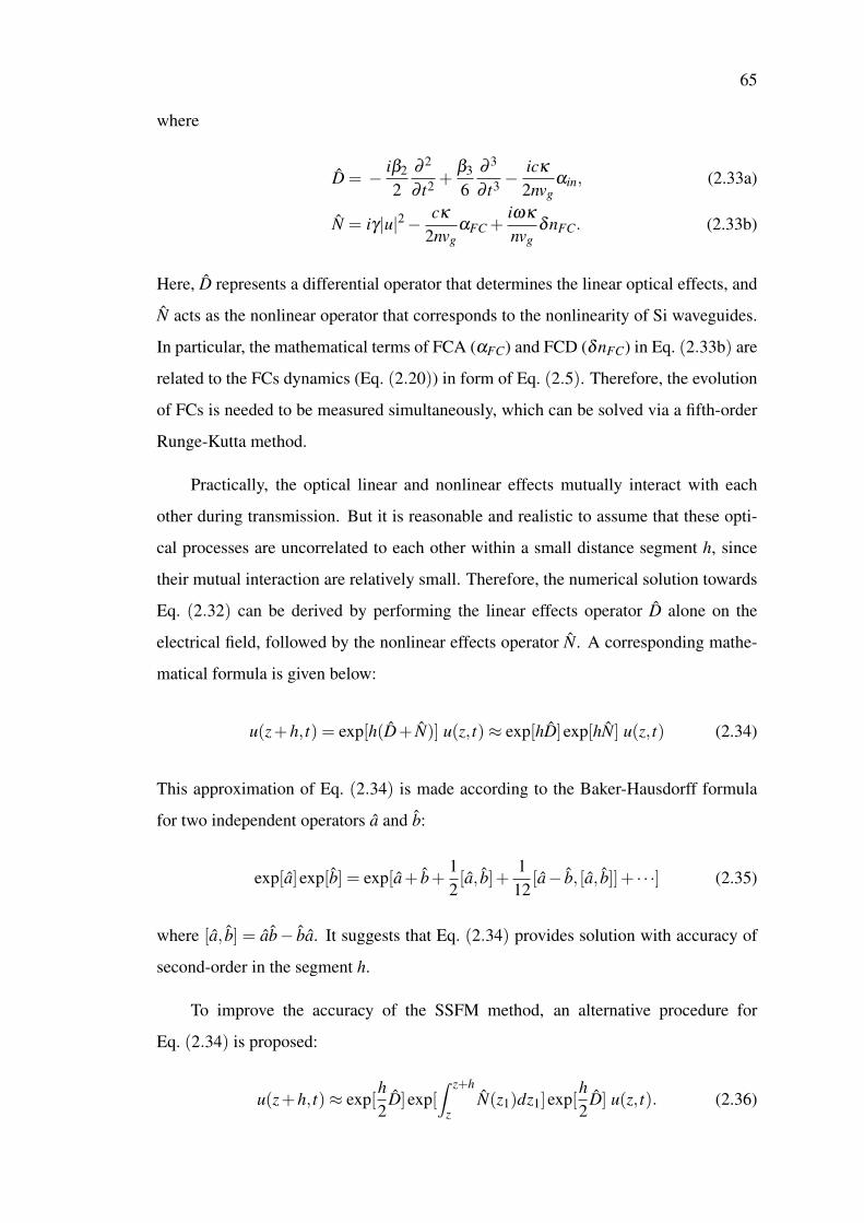
65
where
D = − iβ2
2∂ 2
∂ t2 +β3
6∂ 3
∂ t3 −icκ
2nvgαin, (2.33a)
N = iγ|u|2− cκ
2nvgαFC +
iωκ
nvgδnFC. (2.33b)
Here, D represents a differential operator that determines the linear optical effects, and
N acts as the nonlinear operator that corresponds to the nonlinearity of Si waveguides.
In particular, the mathematical terms of FCA (αFC) and FCD (δnFC) in Eq. (2.33b) are
related to the FCs dynamics (Eq. (2.20)) in form of Eq. (2.5). Therefore, the evolution
of FCs is needed to be measured simultaneously, which can be solved via a fifth-order
Runge-Kutta method.
Practically, the optical linear and nonlinear effects mutually interact with each
other during transmission. But it is reasonable and realistic to assume that these opti-
cal processes are uncorrelated to each other within a small distance segment h, since
their mutual interaction are relatively small. Therefore, the numerical solution towards
Eq. (2.32) can be derived by performing the linear effects operator D alone on the
electrical field, followed by the nonlinear effects operator N. A corresponding mathe-
matical formula is given below:
u(z+h, t) = exp[h(D+ N)] u(z, t)≈ exp[hD]exp[hN] u(z, t) (2.34)
This approximation of Eq. (2.34) is made according to the Baker-Hausdorff formula
for two independent operators a and b:
exp[a]exp[b] = exp[a+ b+12[a, b]+
112
[a− b, [a, b]]+ · · ·] (2.35)
where [a, b] = ab− ba. It suggests that Eq. (2.34) provides solution with accuracy of
second-order in the segment h.
To improve the accuracy of the SSFM method, an alternative procedure for
Eq. (2.34) is proposed:
u(z+h, t)≈ exp[h2
D]exp[∫ z+h
zN(z1)dz1]exp[
h2
D] u(z, t). (2.36)
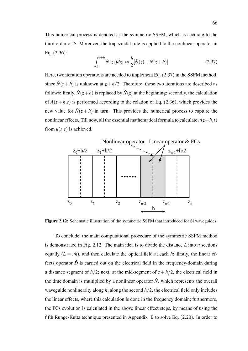
66
This numerical process is denoted as the symmetric SSFM, which is accurate to the
third order of h. Moreover, the trapezoidal rule is applied to the nonlinear operator in
Eq. (2.36): ∫ z+h
zN(z1)dz1 ≈
h2[N(z)+ N(z+h)] (2.37)
Here, two iteration operations are needed to implement Eq. (2.37) in the SSFM method,
since N(z+h) is unknown at z+h/2. Therefore, these two iterations are described as
follows: firstly, N(z+h) is replaced by N(z) at the beginning; secondly, the calculation
of A(z+ h, t) is performed according to the relation of Eq. (2.36), which provides the
new value for N(z+ h) in turn. This provides the numerical process to capture the
nonlinear effects. Till now, all the essential mathematical formula to calculate u(z+h, t)
from u(z, t) is achieved.
z0 z1 z2 znzn-2 zn-1
h
z0+h/2 z1+h/2 zn-1+h/2
Linear operator & FCsNonlinear operator
Figure 2.12: Schematic illustration of the symmetric SSFM that introduced for Si waveguides.
To conclude, the main computational procedure of the symmetric SSFM method
is demonstrated in Fig. 2.12. The main idea is to divide the distance L into n sections
equally (L = nh), and then calculate the optical field at each h: firstly, the linear ef-
fects operator D is carried out on the electrical field in the frequency-domain during
a distance segment of h/2; next, at the mid-segment of z+ h/2, the electrical field in
the time domain is multiplied by a nonlinear operator N, which represents the overall
waveguide nonlinearity along h; along the second h/2, the electrical field only includes
the linear effects, where this calculation is done in the frequency domain; furthermore,
the FCs evolution is calculated in the above linear effect steps, by means of using the
fifth Runge-Kutta technique presented in Appendix B to solve Eq. (2.20). In order to
67
reduce the computational time, the following expression is used to obtain the output
signal after n successive steps:
u(L, t)≈ e−h2 D( n
∏j=1
ehDehN)
eh2 Du(0, t) (2.38)
Additionally, the values of the computational time window, the number of temporal
sampling points (or the FFT points) and the distance step, have to be chosen carefully
in order to ensure the computational accuracy as well as speed up the computational
process. More information about the numerical implementation of this algorithm will
be introduced in Sec. 4.3.1.
2.8.2 Computational Solvers for Ordinary Differential Equations
The Matlab standard solver, ode45, is employed to calculate the ODEs introduced in
Sec. 2.7 [91]. By definition, the Matlab function ode45 is designed to implement the
fifth-order Runge-Kutta routine to solve the typical mathematical problem as follows:
dydt
= f(t,y), y(t0) = y0 (2.39)
Here, t represents the evaluation points, such as time and distance, and y is a t-related
array waiting to be calculated from Eq. (2.39). In this function, the initial conditions of
y(t0) = y0 and the interval of integration tspan are needed to be provided for a specific
mathematical problems.
When considering the propagation of a noisy CW signal in the Si waveguides, the
Matlab function ode45 is used to solve all the coupled first-order ODEs numerically.
For instance, with regard to Eqs. (2.26) and (2.27) for single-channel signal propaga-
tion, we can firstly select four important vector variables as A = P, B = Φ, C = A′ and
D = A′′. Then, based on their interrelations explained in such form:
D↔C↔ A→ B (2.40)
the simplified version of the first-order ODEs (Eqs. (2.26) and (2.27)) can be derived
68
below, with the evaluation points to be the distance z:
dAdz
= f1(A), (2.41a)
dBdz
= f2(A), (2.41b)
dCdz
= f3(A,C,D), (2.41c)
dDdz
= f4(A,C,D), (2.41d)
where the initial conditions, A(0) = A0 stands for the input power of CW signals,
B(0) = B0 represents the initial global phase of optical signal, C(0) = C0 and D(0) =
D0 are the real and imaginary part of the input white noise in the frequency domain.
Eventually, with the initial condition of y0 = [A0;B0;C0;D0] and the integration interval
of tspan, the solver ode45 can be performed on a Matlab function that is programmed
based on Eq. (2.41). This can facilitate accurate numerical results in an efficient way.
Importantly, tspan can be designed in a form of tspan = [t0, t1, t2, · · · , t f ], in order to
control the distance step. In addition, the number of sampling points in y0 has to be ad-
equately large, aiming at maintaining the accuracy of computation. The mathematical
principle of ode45 is introduced in Appendix B.
69
Bibliography[1] R. A. Soref, and J. P. Lorenzo, “Single-crystal silicon: a new material for 1.3 and
1.6 µm integrated-optical components,” Electron. Lett. 21, 953-954 (1985).
[2] G. V. Treyz, P. G. May and J. M. Halbout, “Silicon optical modulators at 1.3 µm
based on free-carrier absorption,” IEEE Electron Device Lett. 12, 276-278
(1991).
[3] B. L. Weiss, Z. Yang, and F. Namavar, “Wavelength dependent propagation
loss characteristics of SiGe/Si planar waveguides,” Electron. Lett. 28, 2218-2220
(1992).
[4] S. Y. Chou, and W. Deng, “Subwavelength amorphous silicon transmission grat-
ings and applications in polarizers and waveplates,” Appl. Phys. Lett. 67, 742-745
(1995).
[5] V. S.-Y. Lin, K. Motesharei, K.-P. S. Dancil, M. J. Sailor, and M. R. Chadiri, “A
Porous Silicon-Based Optical Interferometric Biosensor,” Science 278, 840-842
(1997).
[6] B. E. Little, J. S. Foresi, G. Steinmeyer, E. R. Thoen, S. T. Chu, H. A. Haus, E.
P. Ippen, L. C. Kimerling, and W. Greene, “Ultra-Compact Si−SiO2 Microring
Resonator Optical Channel Dropping Filters ,” Science 278, 840-842 (1997).
[7] C. R. Giles, V. Aksyuk, B. Barber, R. Ruel, L. Stulz and D. Bishop, “A silicon
MEMS optical switch attenuator and its use in lightwave subsystems,” IEEE J.
Sel. Top. Quantum Electron. 5, 18-2 (1999).
[8] T. Shoji, T. Tsuchizawa, T. Watanabe, K. Yamada and H. Morita, “Low loss mode
size converter from 0.3 µm square Si wire waveguides to singlemode fibres,”
Electron. Lett. 38, 1669-1670 (2002).
[9] S. M. Csutak, J. D. Schaub, W. E. Wu, and J. C. Campbell, “High-speed mono-
lithically integrated silicon optical receiver fabricated in 130− nm CMOS tech-
nology,” IEEE Photon. Technol. Lett. 24, 516-518 (2002).
70
[10] D. Taillaert, P. Bienstman, and R. Baets, “Compact efficient broadband grating
coupler for silicon-on-insulator waveguides,” Opt. Lett. 29, 2749-2751 (2004).
[11] I. Kiyat, A. Aydinli, and N. Dagli, “A Compact Silicon-on-Insulator Polarization
Splitter,” IEEE Photon. Technol. Lett. 17, 100-102 (2005).
[12] X. Liu, R. M. Osgood, Y. A. Vlasov, and W. M. J. Green, “Mid-infrared optical
parametric amplifier using silicon nanophotonic waveguides,” Nat. Phot. 4, 557-
560 (2010).
[13] W. Bogaerts, D. Taillaert, B. Luyssaert, P. Dumon, J. Campenhout, P. Bienstman,
D. Thourhout, R. Baets, V. Wiaux, and S. Beckx, “Basic structures for photonic
integrated circuits in Silicon-on-insulator,” Opt. Express 12, 1583-1591 (2004).
[14] Hui Chen, “Silicon Photonic Devices for On-chip Optical Interconnects,” Ph. D.
Thesis ( Hong Kong University of Science and Technology, 2010).
[15] G. T. Reed, G. Z. Mashanovich, W. R. Headley, B. Timotijevic, F. Y. Gardes, S.
P. Chan, P. Waugh, N. G. Emerson, C. E. Png, M. J. Paniccia, A. Liu, D. Hak, and
V. M. N. Passaro, “Issues associated with polarization independence in silicon
photonics,” IEEE J. Sel. Top. Quantum Electron. 12, 1335-1344 (2006).
[16] Y. A. Vlasov, and S. J. McNab, “Losses in sinlge-mode silicon-on-insulator strip
waveguides and bends,” Opt. Express 12, 1622-1631 (2004).
[17] G. Li, J. Yao, Y. Luo, H. Thacker, A. Mekis, X. Zheng, I. Shubin, J.-H. Lee, K.
Raj, J. E. Cunningham, and A. V. Krishnamoorthy, “Ultralow-loss, high-density
SOI optical waveguide routing for macrochip interconnects,” Opt. Express 20,
12035-12039 (2012).
[18] R. W. Boyd, Nonlinear Optics 2nd ed. (2002).
[19] X. Chen, N. C. Panoiu, and R. M. Osgood, “Theory of Raman-mediated pulsed
amplification in silicon-wire waveguides,” IEEE J. Quantum Electron. 42, 160-
170 (2006).
71
[20] E. Dulkeith, F. Xia, L. Schares, W. M. J. Green, and Y. A. Vlasov, “Group in-
dex and group velocity dispersion in silicon-on-insulator photonic wires,” Opt.
Express 14, 3853-3863 (2006).
[21] X. Chen, N. C. Panoiu, I. Hsieh, J. I. Dadap, and R. M. Osgood, “Third-order dis-
persion and ultrafast pulse propagation in silicon wire waveguides,” IEEE Photon.
Technol. Lett. 18, 2617-2619 (2006).
[22] G. P. Agrawal, Nonlinear Fiber Optics 4th ed., Academic Press (2006).
[23] R. M. Osgood, N. C. Panoiu, J. I. Dadap, X. Liu, X. Chen, I-W. Hsieh, E. Dulkeith,
W. M. J. Green, and Y. A. Vlassov, “Engineering nonlinearities in nanoscale op-
tical systems: physics and applications in dispersion-engineered silicon nanopho-
tonic wires,” Adv. Opt. Photon. 1, 162-235 (2009).
[24] T. R. Taha, and M. J. Ablowitz, “Analytical and numerical aspects of certain
nonlinear evolution equations. II. Numerical, nonlinear Schrodinger equation,”J.
Comput. Phys. 55, 203-230 (1984).
[25] J. Zhang, Q. Lin, G. Piredda, R. W. Boyd, G. P. Agrawal, and P. M. Fauchet, “
Anisotropic nonlinear response of silicon in the near-infrared region,” Appl. Phys.
Lett. 91, 071113 (2007).
[26] M. P. Chethiya, M. Dissanayake, I. D. Rukhlenko, and G. P. Agrawal, “FDTD
modeling of anisotropic nonlinear optical phenomena in silicon waveguides,” Opt.
Express 18, 21427-21448 (2010).
[27] X. Chen, N. C. Panoiu, and R. M. Osgood, “ Theory of Raman-mediated pulsed
amplification in silicon- wire waveguides,” IEEE J. Quantum Electron. 42, 2889-
2891 (2008).
[28] I.-W. Hsieh, X. Chen, J. I. Dadap, N. C. Panoiu, R. M. Osgood, S. J. McNab, and
Y. A. Vlasov, “Ultrafast-pulse self-phase modulation and third-order dispersion in
Si photonic wire-waveguides,” Opt. Express 14, 12380-12387 (2006).
[29] L. Y and G. P. Agrawal, “Impact of two-photon absorption on self-phase modula-
tion in silicon waveguides,” Opt. Lett. 32, 2031-2033 (2007).
72
[30] N. C. Panoiu, J. F. McMillan, and C. W. Wong, “Theoretical analysis of pulse dy-
namics in silicon photonic crystal wire waveguides,” IEEE J. Sel. Top. Quantum
Electron. 16, 257-266 (2010).
[31] I.-W. Hsieh, X. Chen, J. I. Dadap, N. C. Panoiu, R. M. Osgood, S. J. McNab, and
Y. A. Vlasov, “Cross-phase modulation-induced spectral and temporal effects on
co-propagating femtosecond pulses in silicon photonic wires,” Opt. Express 15,
1135-1146 (2007).
[32] Y. Zhang, C. Husko, S. Lefrancois, I. H. Rey, T. F. Krauss, J. Schr oder, and
B. J. Eggleton, “Cross-phase modulation-induced spectral broadening in silicon
waveguides,” Opt. Express 24, 443C451 (2016).
[33] S. Lavdas, “Optical pulse dynamics in sub-wavelength nano-patterned silicon
photonic wires,” Ph. D. Thesis (University College London, 2015).
[34] R. A. Soref and B. R. Bennett, “Electro-optical effects in silicon,” IEEE J. Quan-
tum Electron. QE-23, 123-129 (1987).
[35] P. E. Barclay, K. Srinivasan, and O. Painter, “Nonlinear response of silicon pho-
tonic crystal microresonators excited via an integrated waveguide and fiber taper,”
IEEE J. Quantum Electron. 13, 801-820 (2005).
[36] Rsoft Design Group, Femsim, https://optics.synopsys.com/
rsoft/rsoft-passive-device-femsim.html.
[37] J. D. Joannopoulos, S. G. Johnson, J. N. Winnn, and R. D. Meade, Photonic
Crystals: Modeling the Flow of Light (Princeton University Press, 2008).
[38] T. F. Krauss, “Why do we need slow light?,” Nat. Phot. 2, 448-450 (2008).
[39] T. Baba, “Slow light in photonic crystals,” Nat. Phot. 2, 465-473 (2008).
[40] G. P. Agrawal, Fiber-Optic Communication Systems 3rd ed. (Wiley, 2002).
[41] V. R. Almeida, C.A. Barrios, R. R. Panepucci, and M. Lipson, “All-optical control
of light on a silicon chip,” Nature 431, 1081-1084 (2004).
73
[42] S. R. Preble, Q. Xu, B. S. Schmidt, and M. Lipson, “Ultrafast all-optical modula-
tion on a silicon chip,” Opt. Lett. 30, 2891-2893 (2005).
[43] D. Liang, M. Fiorentino, T. Okumura, H.-H. Chang, D. T. Spencer, Y.-H. Kuo,
A. W. Fang, D. Dai, R. G. Beausoleil, and J. E. Bowers,“Electrically-pumped
compact hybrid silicon microring lasers for optical interconnects,” Opt. Express
17, 20355-20364 (2009).
[44] R. Claps, D. Dimitropoulos, V. Raghunathan, Y. Han, and B. Jalali, “Observation
of stimulated Raman amplification in silicon waveguides,” Opt. Express 11, 1731-
1739 (2003).
[45] R. Espinola, J. I. Dadap, R. M. Osgood, S. J. McNab, and Y. A. Vlasov, “Raman
amplification in ultrasmall silicon-on-insulator wire waveguides,” Opt. Express
12, 3713-3718 (2004).
[46] A. Liu, R. Jones, L. Liao, D. Samara-Rubio, D. Rubin, O. Cohen, R. Nicolaescu,
and M. Paniccia, “A high-speed silicon optical modulator based on a metal-oxide-
semiconductor capacitor,” Nature 427, 615-618 (2004).
[47] C. Manolatou, and M. Lipson, “All-optical silicon modulators based on carrier
injection by two-photon absorption,” IEEE J. Lightwave Technol. 24, 1433-1439
(2006).
[48] P. D. Trinh, S. Yegnanarayanan, F. Coppinger, and B. Jalali, “Silicon-on-
Insulator (SOI) Phased-Array Wavelength Multi/Demultiplexer with Extremely
Low-Polarization Sensitivity,” IEEE Photon. Technol. Lett. 9, 940-942 (1997).
[49] R. L. Espinola, M.-C. Tsai, J. T. Yardley, and R. M. Osgood Jr., “Fast and low-
power thermooptic switch on thin silicon-on-insulator,” IEEE Photon. Technol.
Lett. 15, 1366-1368 (2005).
[50] O. Boyraz, P. Koonath, V. Raghunathan, and B. Jalali, “All optical switching and
continuum generation in silicon waveguides,” Opt. Express 12, 4094-4102 (2004).
[51] B. G. Lee, A. Biberman, P. Dong, M. Lipson, and K. Bergman, “All-optical comb
74
switch for multiwavelength message routing in silicon photonic networks,” IEEE
Photon. Technol. Lett. 20, 767-769 (2008).
[52] T. Tanabe, M. Notomi, S. Mitsugi, A. Shinya, and E. Kuramochi, “All-optical
switches on a silicon chip realized using photonic crystal nanocavities,” Appl.
Phys. Lett. 87, 151112 (2005).
[53] P. C. P. Chen, A. M. Pappu, and A. B. Apsel, “Monolithic integrated SiGe optical
receiver and detector,” Proc. Conf. Lasers and Electro-Optics, Tech. Dig. (CD)
(Optical Society of America) CTuZ4, 1-2 (2007).
[54] S. Assefa, F. Xia, W. M. J. Green, C. L. Schow, A. V. Rylyakov, and Y. A. Vlasov,
“CMOS-Integrated Optical Receivers for On-Chip Interconnects,” IEEE J. Sel.
Top. Quantum Electron. 16, 1376-1385 (2010).
[55] H. Fukuda, K. Yamada, T. Shoji, M. Takahashi, t. Tsuchizawa, T. Watanabe, J.
Takahashi, and S. Itabashi, “Four-wave mixing in silicon wire waveguides,” Opt.
Express 13, 4629-4637 (2005).
[56] S. Zlatanovic, J. S. Park, S. Moro, J. M. C. Boggio, I. B. Divliansky, N. Alic,
S. Mookherjea, and S. Radic, “Mid-infrared wavelength conversion in silicon
waveguides using ultracompact telecom-band-derived pump source,” Nat. Phot.
4, 561-564 (2010).
[57] O. V. Sinkin, “Calculation of Bit Error Rates in Optical Fiber Communicatons
Systems in the Presence of Nonlinear Distortion and Noise,” Ph. D. Thesis (Uni-
versity of Maryland, 2006).
[58] J. Wang, “Performance Evluation of DPSK Optical Fiber Communication sys-
tem,” Ph.D. Thesis (University of California, 2004).
[59] J. P. Winzer and R. J. Essiambre, “Advanced optical modulation formats,” Proc.
IEEE 94, 952-985 (2006).
[60] M. Rohde, C. Caspar, N. Heimes, M. Konitzzer, E. J. Bachus, and N. Hanik, “Ro-
bustness of DPSK direct detection transmission format in standard fiber WDM
systems,” Electron. Lett. 36, 1483-1484 (2000).
75
[61] J. Wang, and J. M. Kahn, “Impact of Chromatic and Polarization-Mode Disper-
sions on DPSK Systems Using Interferometric Demodulation and Direct Detec-
tion,” IEEE J. Lightwave Technol. 22, 362-371 (2004).
[62] M. Nolle, M. Seimetz, and E. Patzak, “System Performance of High-Order Op-
tical DPSK and Star QAM Modulation for Direct Detection Analyzed by Semi-
Analytical BER Estimation,” IEEE J. Lightwave Technol. 27, 4319-4329 (2009).
[63] M. Seimetz, M. Nolle, and E. Patzak, “Optical System With High-Order Optical
DPSK and Star QAM Modulation Based on Interferometric Direct Detection,”
IEEE J. Lightwave Technol. 25, 1515-1530 (2007).
[64] S. Lavdas and N. C. Panoiu, “Theory of Pulsed Four-Wave-Mixing in One-
dimensional Silicon Photonic Crystal Slab Waveguides,” Phys. Rev. B 93, 115435
(2016).
[65] C. Koos, L. Jacome, C. Poulton, J. Leuthold, W. Freude, “Nonlinear silicon-on-
insulator waveguides for all-optical signal processing,” Opt. Express 15, 5976-
5990 (2007).
[66] J. I. Dadap, N. C. Panoiu, X. G. Chen, I. W. Hsieh, X. P. Liu, C. Y. Chou, E.,
Dulkeith, S. J., McNab, F. N. Xia, W. M. J. Green, L. Sekaric, Y. A. Vlasov, and
R. M. Osgood, “Nonlinear-optical phase modification in dispersion-engineered Si
photonic wires,” Opt. Express 16, 1280-1299 (2008).
[67] A. W. Snyder and J. D. Love, Optical Waveguide Theory (Chapman & Hall, 1983).
[68] N. C. Panoiu, J. F. McMillan, and C. W. Wong, “Theoretical analysis of pulse dy-
namics in silicon photonic crystal wire waveguides,” IEEE J. Sel. Top. Quantum
Electron. 16, 257-266 (2010).
[69] V. S. Afshar, T. M. Monro, and C. M. de Sterke, “Understanding the contribution
of mode area and slow light to the effective Kerr nonlinearity of waveguides,”
Opt. Express 21, 18558-18571 (2013).
[70] G. Bosco, A. Carena, V. Curri, R. Caudino, P. Poggiolini, and S. Benedetto, “A
76
Novel Analytical Method for the BER Evaluation in Optical Systems Affected by
Parametric Gain,” IEEE Photon. Technol. Lett. 12, 152-154 (2000).
[71] G. Bosco, A. Carena, V. Curri, R. Caudino, P. Poggiolini, and S. Benedetto, “Para-
metric Gain in Multiwavelength Systems: A New Approach to Noise Enhance-
ment Analysis,” IEEE Photon. Technol. Lett. 11, 1135-1137 (1999).
[72] J. You, and N. C. Panoiu, “Calculation of Bit Error Rates in Optical Systems with
Silicon Photonic Wires,” IEEE J. Quantum Electron. 51, 8400108 (2015).
[73] J. You and N. C. Panoiu, “Exploiting Higher-order Phase-shift Keying Modulation
and Direct-detection in Silicon Photonic Systems,” Opt. Express 25, 8611-8624
(2017).
[74] Q. Lin, Oskar J. Painter, and Govind P. Agrawal, “Nonlinear optical phenomena in
silicon waveguides: modeling and applications,” Opt. Express 15, 16604-16644
(2007).
[75] J. You, S. Lavdas, and N. C. Panoiu, “Comparison of BER in Multi-channel Sys-
tems With Strip and Photonic Crystal Silicon Waveguides,” IEEE J. Sel. Top.
Quantum Electron. 22, 4400810 (2016).
[76] R. Hui, D. Chowdhury, M. Newhouse, M. O’Sullivan, and M. Pettcker, “Nonliear
amplification of noise in fibers with dispersion and its imipact in optical amplified
systems,” IEEE Photon. Technol. Lett. 9, 392-394 (1997).
[77] E. A. Golovchenko, A. N. Pilipetskii, N. S. Bergano, C. R. Davidsen, F. I. Kha-
tri, R. M. Kimball, and V. J. Mazurczyk, “Modeling of transoceanic fiber-optic
WDM communications systems,” IEEE J. Sel. Top. Quantum Electron. 6, 337-
347 (2000).
[78] R. Holzl ohner, V. S. Grigoryan, C. R. Menyuk, and W. L. Kath, “Accurate cal-
culation of eye diagrams and bit error rates in optical transmission systems using
linearization,” IEEE J. Lightwave Technol. 20, 389-400 (2002).
77
[79] E. Forestieri, “Evaluating the error probability in lightwave systems with chro-
matic dispersion, arbitrary pulse shape and pre- and postdetection filtering,” IEEE
J. Lightwave Technol. 18, 1498-1503 (2000).
[80] B. A. Berg and T. Neuhaus, “Multicanonical ensemble: A new approach to simu-
late first-order phase transitions,” Phys. Rev. Lett. 68, 9-12 (1992).
[81] B. A. Berg , “Algorithmic aspects of multicanonical Monte Carlo simulations,”
Nucl. Phys. Proc. Suppl. 63, 982-984 (1998).
[82] G. Bosco, A. Carena, V. Curri, R. Gaudino, P. Poggiolini, and S. Benedetto, “A
novel analytical approach to the evaluation of the impact of fiber parametric gain
on the bit error rate,” IEEE Trans. Commun. 49, 2154-2163 (2001).
[83] E. Forestieri and M. Secondini, “On the Error Probability Evaluation in Lightwave
Systems With Optical Amplification,” IEEE J. Lightwave Technol. 27, 706-717
(2009).
[84] J–S. Lee and C–S. Shim, “Bit-error-rate analysis of optically preamplified re-
ceivers using an eigenfunction expansion method in optical frequency domain,”
IEEE J. Lightwave Technol. 12, 1224-1229 (1994).
[85] A. Mafi and S. Raghavan, “Nonlinear phase noise in optical communication
systems using eigenfunction expansion method,” Opt. Engineering 50, 055003
(2011).
[86] C. W. Helstrom, “Approximate evaluation of detection probabilities in radar and
optical communication,” IEEE Trans. Aerosp. Electron. Syst. 14, 630-640 (1978).
[87] A. Papoulis, Probability, Random Variables, and Stochastic Processes 3rd ed,
(McGraw-Hill, New York, 1991).
[88] C. W. Helstrom, Statistical Theory of Signal Detection (Pergamon, New York,
1968).
[89] A. M. Mathai and S. B. Provost, Quadratic Forms in Random Variables (Marcel
Dekker, New York, 1992).

78
[90] C. W. Helstrom, “Distribution of the Filtered Output of a Quadratic Rectifier Com-
puted by Numberical Contour Integration,” IT-32, 450-463 (1986).
[91] Matlab version R2016b, ODE45, https://uk.mathworks.com/help/
matlab/ref/ode45.html.
Chapter 3
Mathematical Concepts Used in BER
Calculation
3.1 IntroductionThe nonlinearity would normally exist in the current waveguides and receivers, and
even in the next-generation optical communication nextworks, which only allow for
small bit-rate transmission. This suggests that neither traditional analytical approaches
nor standard Monte-Carlo methods are suitable for BER calculation in the systems
mentioned above. To date, some new BER calculation methods have been proposed to
account for the influence of waveguide nonlinearity, noise and signal patterns. Specif-
ically, these calculation mechanisms can be categorized into four types: (1) CW noise
method. This method was initially proposed by Hui et al. [1], and only designed for
the CW optical signals. Its main idea is to separate the noise amplification from nonlin-
ear optical effects by using mathematical manipulation. (2) Covariance matrix method.
This approach was originally raised by Holzloehner et al. [2] for the BER estimation
in a highly nonlinear optical system via linearization. (3) Receiver model. This numer-
ical algorithm has been developed by Bosco et al. [3] and Forestieri et al. [4] for the
calculation of BER in the optical pre-amplified receivers. (4) Multicanonical Monte
Carlo method. This numerical scheme was firstly introduced by Berg et al. [5, 6], and
is based on the efficient biased Monte Carlo simulations. In this chapter, several KLSE
approaches will be presented to compute the BER for both single- and multi-channel
optical systems. Specifically, these methods can be performed via the time-domain
[7–9], frequency-domain [9–11] and Fourier-series routines [4]. A major advantage of
80
these KLSE methods is their capability of characterizing various factors that influence
the system BER [12], e.g., waveguide nonlinearity.
This chapter is organized as follows. The mathematical formulation of the time-
domain KLSE method designed for the CW signals will be introduced in Sec. 3.2.
Similarly, Sec. 3.3 will describe another KLSE method for the evaluation of CW signals
via the frequency domain. In addition, Sec. 3.4 will present the Fourier-series KLSE
method for the analysis of all types of signal modulation formats. In the last section,
a specific computational approach, denoted as the saddle-point approximation, will be
introduced for the BER calculation. This algorithm is based on the moment-generating
function (MGF) from Sec. 3.2, Sec. 3.3 and Sec. 3.4.
3.2 Time-domain Karhunen-Loeve Expansion MethodThe time-domain KLSE serves as an efficient approach to calculate the transmission
BER at the back-end of the receiver. As mentioned earlier, this numerical approach is
constructed only for the estimation of CW optical signals. According to the schematic
of a single-channel OOK system shown in Fig. 2.10, a generic direct-detection receiver
is composed of a Lorentzian optical filter with impulse response, ho(t), followed by an
ideal photodetector and an integrate-and-dump electrical filter, whose impulse response
is he(t). However, the receiver configuration is more complicated for the PSK optical
signals, with more details discussed in Sec. 7.3. Notably, the electrical noises of the
receiver have not been taken into account, as in most cases the thermal and shot noises
can be negligible in the systems where the white noise enhancement plays the domi-
nant role in limiting the system performance [8, 13]. Moreover, in the WDM system
(see Fig. 2.11) we assume that no additional statistical correlations among signal prop-
agating in each channel are introduced during signal demultiplexing. For simplicity,
the case of kth channel is selected to stand for both cases of single-channel and multi-
channel system detection. Note also that this choice of kth channel representation is
also made in the other two KLSE methods described in Sec 3.3 and Sec 3.4.
To start with, we present the complex envelope of the optical signal at the front
of the kth receiver as r1,k(t) = Sk + ai,k(t)+ jaq,k(t), where ai,k(t) and aq,k(t) are the
in-phase and quadrature noise components, respectively, and Sk is the amplitude of the
CW signal. We consider that Sk = 0 (S2k = Pk) when a “0” (“1”) is transmitted, where
81
Pk is the power of optical signals in the kth channel. Moreover, it is assumed that the
carrier propagates unchanged through an optical filter, which amounts to Ho(0) = 1
with Ho( f ) = Fho(t). Hence, the signal after the optical filter can be written as,
r2,k(t) = Sk + vi,k(t)+ jvq,k(t), where vµ,k(t) = ho(t)⊗aµ,k(t)(µ = i,q). After passing
through the ideal square-law photodetector and the electrical filter, the electrical sig-
nal, yk(t) = he(t)⊗|r2,k(t)|2, so that at the back-end of the receiver it is given by the
following expression:
yk(t) =∫
∞
−∞
he(t)[
Sk + vi,k(t− t ′)]2+ v2
q,k(t− t ′)
dt ′. (3.1)
The noise components of kth channel at the output of the waveguide are assumed
to be stationary and completely determined by their power spectral density matrix [14]:
G a,k( f ) =
G ia,k( f ) G iq
a,k( f )
G qia,k( f ) G q
a,k( f )
, (3.2)
where G ia,k and G q
a,k are the power spectral densities of the in-phase and quadrature
noise components from the kth channel, respectively; G iqa,k and G qi
a,k symbolize the cross-
spectral power density, obeying G iqa,k = G qi
a,k. Note that even if at the input of the Si
waveguide the in-phase and quadrature noise components are assumed to be uncorre-
lated, the mutual interaction mediated by the FCs and optical nonlinearity makes them
to become correlated by the time they reach the back-end of the waveguide.
Upon passing through the optical filter, the power spectral density matrix of the
noise, G v,k( f ), becomes [14]:
G v,k( f ) = H o( f ) ·G a,k( f ) ·H †o( f ), (3.3)
where “†” represents Hermitian conjugation operation. The real value optical filter
matrix H o is given by:
H o =
H io( f ) −Hq
o ( f )
Hqo ( f ) H i
o( f )
. (3.4)
where H io( f ) =Fh′o(t) and Hq
o ( f ) =Fh′′o(t) are the Fourier transform of the real
82
and imaginary parts of the optical filter impulse response, respectively.
Next, the signal, Sk, and both components of the noise, vi,k(t) and vq,k(t), are
expanded in KLSE series. The deterministic functions, φ kα(t) and ψk
α(t), will be
defined in the expansions, and are both orthonormal to he(t) [15]:
Sk = ∑α≥1
skαφ
kα(t), (3.5a)
vi,k(t) = ∑α≥1
pkαφ
kα(t), (3.5b)
vq,k(t) = ∑α≥1
qkαψ
kα(t), (3.5c)
where the expansion coefficients, skα, pk
α and qkα, are random variables. By
applying the orthonormality conditions,
∫∞
−∞
he(t)φ kα(t)φ
k,∗β
(t)dt = δαβ , (3.6a)∫∞
−∞
he(t)ψkα(t)ψ
k,∗β
(t)dt = δαβ , (3.6b)
these KLSE expansion coefficients can be proven to be in such forms:
skα = Sk
∫∞
−∞
he(t)φk,∗α (t)dt, (3.7a)
pkα =
∫∞
−∞
he(t)vi,k(t)φk,∗α (t)dt, (3.7b)
qkα =
∫∞
−∞
he(t)vq,k(t)ψk,∗α (t)dt. (3.7c)
What follows is to combine Eqs. (3.1), (3.5) and (3.6) together and use the stationary
condition of vi,k(t) and vq,k(t). Thus, the electrical signal can be rewritten as:
yk = ∑α≥1|sk
α + pkα |
2+ ∑
α≥1|qk
α |2. (3.8)
This equation indicates the fact that the statistics of the electrical signal is com-
pletely determined by the probability distributions of the random variables skα, pk
α
and qkα, which in turn are defined by the functions φ k
α(t) and ψkα(t). Then
our emphasis is shifted to compute φ kα(t) and ψk
α(t). Importantly, the random
variables pkα and qk
α are mutually uncorrelated, namely, Epkα pk,∗
β = µk
αδαβ
83
and Eqkαqk,∗
β = νk
αδαβ . By using simple mathematical manipulations, φ kα(t) and
ψkα(t) are proven to be eigenfunctions of the second kind homogeneous Fredholm
integral equations, with µkα and νk
α to be the corresponding eigenvalues:
∫∞
−∞
he(τ)ρki (t− τ)φ k
α(τ)dτ = µkαφ
kα(t), (3.9a)∫
∞
−∞
he(τ)ρkq(t− τ)ψk
α(τ)dτ = νkαψ
kα(t). (3.9b)
Here, ρki (t) and ρk
q(t) are the autocorrelation functions of the noise functions vi,k(t)
and vq,k(t), respectively, which are symbolized by ρki (t) = F−1G i
v,k and ρq(t) =
F−1G qv,k. In order to find numerical solutions for Eqs. (3.9), the Gauss-Hermite
quadrature method (see Appendix. A) is employed to calculate the integrals. Simulta-
neously, the time variable t is discretized over the same grid points as the abscissas τl
in the Gauss-Hermite quadrature method, namely, tl = τl, l = 1, . . . ,M. To this point,
this problem is transferred to find the eigenvalues (µkα, νk
α) and eigenfunctions
(φ kα(tl), ψk
α(tl)) for the two resulted matrix. However, the in-phase and quadra-
ture noise components turn to be correlated after propagation, Epkαqk,∗
β ≡ σ k
αβ6= 0.
which should also be included in the computational analysis. Then, by performing
mathematical operations on Eqs. (3.7), we can easily derive the following relation:
∫∞
−∞
he(t)he(τ)ρkiq(τ− t)ψk
β(τ)dτ = ∑
α≥1σ
kαβ
φkα(t), (3.10)
where ρkiq(t) stands for the cross correlation between vi,k(t) and vq,k(t), with the expres-
sion of ρkiq(t) = F−1G iq
v,k. Similarly, the Gauss-Hermite quadrature technique is also
operated on Eq. (3.10). By solving the resulted linearized equations, we can obtain the
matrix σ kαβ. Hence, the complete form of the noise correlation matrix, Rk, can be
derived after direct-detection:
Rk =
Λkµ Σ
k
Σk,† Λkν
, (3.11)
where Λkµ = diag(µk
α) and Λkν = diag(νk
α) are diagonal matrices and Σkαβ
= σ kαβ
.
The last step is to discretize the analytical formula mentioned above, in order
84
to derive the semi-analytical solution rigorously. First of all, after the optical filter,
the complex noise is written as a column vector, nk = [pk1 · · · pk
M qk1 · · ·qk
M]T ( T is the
transpose operation, unless otherwise is specified), containing two random variables
(pkα and qk
α). In the meanwhile, the signal is expressed as sk = [sk1 · · ·sk
M 0 · · ·0]T .
Thus, the electrical current Eq. (3.8) can be written in a new form:
yk = xk† · xk =
2M
∑α=1|xk
α |2, (3.12)
where xk = [xk1 · · ·xk
2M]T ≡ nk + sk. Note that the signal and the noise are uncorrelated,
Enkαsk,∗
β = 0, and also Enk
α = 0, ∀α,β = 1 . . .2M. Secondly, a unitary matrix Uk
is used to diagonalize the correlation matrix Rk, obtaining an ideal diagonal matrix
∆k = diag(δ k
α):
Uk,† Rk Uk = ∆k, (3.13)
where δ kα(α = 1 . . .2M) are the eigenvalues of Rk. Since the unitary matrix Uk con-
serves to the norm of vectors, Eq. (3.12) can be recast into:
yk = wk† ·wk =
2M
∑α=1|wk
α |2, (3.14)
where wk =Uk,†xk. Then, the statistical properties of wk can be easily obtained:
Ewk=Uk,† Enk + sk=Uk,† sk ≡ ηk = [ηk1 · · ·ηk
2M]T , (3.15a)
Ewk ·wk†=Uk,† Exk · xk
†Uk =Uk,† Rk Uk = ∆k. (3.15b)
From Eq. (3.15b), one can see that the noise correlation matrix wkα is diagonal. To
calculate the BER, the MGF, Ψyk(ζ ), is calculated for the random variable yk [16]:
Ψyk(ζ ) = Ee−ζ yk=2M
∏α=1
exp(− |η
kα |
2ζ
1+2δ kα ζ
)√
1+2δ kαζ
, (3.16)
where δ kα are the eigenvalues of the correlation matrix, and ηk
α are the average values of
yk from Eq. (3.14). The detailed mathematical process of calculating the system BER
85
from the MGF will be described in Sec. 3.5.
3.3 Frequency-domain Karhunen-Loeve Expansion
The frequency-domain KLSE method [11] is presented in this section, aiming at esti-
mating the BER performance of Si photonic systems in a accurate and efficient way.
This algorithm is only designed for the CW optical signals, in presence of the complex
white noise. When compared with the time-domain method described in Sec 3.2, this
method shows strength in its good transferability for more complicated optical systems.
Here, the kth channel is selected to be the representative for both cases of single- and
multi-channel detection.
Before proceeding to construct the mathematical models, the configuration of the
direct-detection receiver is specified in the frequency domain: a lorentzian optical
filter, Ho( f ), an ideal square-law photodetector and an integrate-and-dump electrical
filter, He( f ). Particularly, Ho( f ) and He( f ) are the Fourier transform of ho(t) and
he(t), which are impulse response function of optical and electrical filters mentioned in
Sec. 3.2. Here, Xk( f ) is defined as the Fourier transform of the receiver input signals
xk(t). Therefore, the photocurrent at the output of the receiver can be written as:
yk(t) =∫
∞
−∞
∫∞
−∞
X∗k ( f1)D( f1, f2)Xk( f2)e2π j( f2− f1)td f1d f2 (3.17)
where the Hermitian kernel D represents the receiver functionalities, including an op-
tical filter, an electrical filter and a photodetector, which is given by:
D = H∗o ( f1)He( f2− f1)Ho( f2), (3.18)
As suggested in Sec. 3.2, the derivation of the MGF is indeed the fundamental part of
the BER calculation when using the KLSE method. In order to determine the MGF of
yk(t), the crucial step is to compute the correlation matrix Rk in frequency domain. To
fulfil this goal, we firstly discretize the Hermitian kernel and the electrical field with a
step δ f : Dm,n = D( fm, fn)δ f , xk,n = Xk( fn)e2πi fnt√
δ f , where fm = mδ f , fn = nδ f
(m,n =−Q, ...,Q, Q is a large integer). Thus, the Eq. (3.17) can be expressed in a new
86
form:
yk(t) =Q
∑m,n=−Q
x∗k,m Dm,n xk,n, (3.19)
Secondly, we recast the new electrical field xk,n into a real-value form: xk =
(x′k,−Q, ..., x′k,Q, x
′′k,−Q, ..., x
′′k,Q)
T . In this dissertation, ′ and ′′ denote the real and imag-
inary part of a physical variable, unless otherwise is specified. And the real-value
receiver matrix is symbolized as W = [D′,−D
′′;D ′′,D ′]. Thus, the decision vari-
able yk(t) can be written in the new form, yk(t) = xkT W xk. Moreover, the optical
signal at the input of the receiver is expressed as xk(t) = Sk +ai,k(t)+ jaq,k(t), as men-
tioned in Sec 3.2. Then, the Fourier transform of the noise ai,k + jaq,k is denoted as
ARI = (AR, AI)T , where AR and AI are real. The Fourier transform of ai,k and aq,k are
given by AR and AI , respectively, forming a new complex variable ARI = (AR, AI)T .
More details about ARI and ARI can be found in [11]. It can be proved mathematically
that the power spectral density matrix Skk of noise can be expressed in such form:
Skk(z,ω) =⟨
ARI (z,ω)ARI(z,ω)†⟩, (3.20)
Note that Skk obeys such symmetric properties: S†kk(z,ω) = Skk(z,ω), S∗kk(z,ω) =
Skk(z,−ω). Regarding the new noise form, A±RI = [AR(ω), AR(−ω), AI(ω), AI(−ω)]T ,
the cross correlation matrix is derived mathematically:
Fk(ω) =⟨A±RI A±T
RI⟩=
s+ t
t s−
, (3.21)
where s± = S11kk (ω)1±σ1
2 + S22kk (ω)1∓σ1
2 + Im[S12kk (ω)]σ3, t = Re[S12
kk (ω)]σ1. Here, σ1,
σ2 and σ3 stand for 2×2 Pauli matrices. Due to the symmetry properties of Skk, we only
need to calculate the elements of Eq. (3.21) with ω ≥ 0. To this end, the correlation
matrix Rk can be obtained by using mathematical manipulation of Fk, according to
relation listed below:
(Rk)
ρa,ρb
= (Fk)ab|ω=2π fn
ρa = (1+n,2Q+1−n,2Q+2+n,4Q+2−n),
87
n = 0, ...,2Q,
a,b =1, ...,4
(3.22)
Furthermore, the Cholesky factorization is utilized to decompose the correlation matrix
Rk in form of a lower triangular matrix L , i.e., Rk = L L T . To diagonalize the real
symmetric matrix L T W L , an orthogonal matrix U is used to obtain eigenfunctions
and eigenvalues:
(U T L T W L U )p,q = Λ (3.23)
where Λ = diag(λ1, ... ,λ4Q+2), with λp (p = 1, ...,4Q+ 2) real value. Moreover, the
total electric field xk is composed of signal sk and noise nk, where⟨nk⟩= 0 and
⟨xk⟩=
sk. Thus, according to Eq. (3.23), the new signal and noise elements can be obtained:
zk = U T L −1(xk− sk), (3.24a)
ζk = U T L −1sk, (3.24b)
Hence, the decision variable ik(t) can be rewritten in a simple form:
yk(t) =4Q+2
∑n=1
λn(zk,n +ζk,n)2, (3.25)
Therefore, by combining the analysis towards the signal sk, the noise nk, the shift vari-
able ζk, the decision variable yk(t) and the correlation matrix Rk, the MGF in frequency
domain, Ψyk(s), is obtained:
Ψyk(s) =4Q+2
∏n=1
exp(
λn|ζk,n|2s√1−2λns
)√
1−2λns, (3.26)
In the end, the system BER can be computed by applying the mathematical technique
introduced in Sec. 3.5 on Eq. (3.26).
88
3.4 Fourier-series Karhunen-Loeve Expansion
The Fourier-series KLSE approach [4] is described in this section to quantify the system
BER after the direct-detection receivers. As a complementary, the perturbation theory
is first used to characterize the transmission matrix and further the noise correlation
matrix in the central channel of single- and multi-channel transmission systems. In
this section, we select the kth channel to be the central channel, and carry out the
BER calculation in the kth channel to represent both single- and multi-channel systems.
Specifically, the central channel refers to the kth channel for the M-channel photonic
systems, where k = M/2 when M is an even integer, or k = (M−1)/2 when M is odd.
As for the single-channel systems, the central channel is itself.
Before we describe the mathematical approach for system BER calculation, we
present the perturbation theory used to determine the noise dynamics in Si waveg-
uides. To this end, we express the complex envelope of the optical field at the input of
the waveguide as xk(t) = sk(t)+wk(t), where sk(t) = 〈xk(t)〉 represents the noise-free
signal and wk(t) is the complex additive white Gaussian noise. Here, the symbol 〈·〉
denotes the statistical expectation operator. Furthermore, the noise wk is expanded in
Fourier series, namely, wk = ∑N/2−1l=−N/2 nl,ke jΩlt , where Ωl = 2πl/Ttot and Ttot = NtotT0,
with Ntot being the total number of transmitted bits. Then, a (4Q+ 2)-dimensional
noise Fourier vector is defined as, wk = (n′−Q,k, . . . ,n′Q,k,n
′′−Q,k, ...,n
′′Q,k)
T , where xT de-
notes the transpose of x. Importantly, in order to reduce the computational time, Q is
chosen such that 2Q+ 1 is more than 100 times smaller than N. The reason why this
is a valid choice is that most of the information pertaining to the noise can be collected
from the central part of the spectra.
The next step of the algorithm is to calculate the noise covariance matrix, Rk =⟨wk wk
T⟩, at the output of the waveguide. This can be expressed in terms of Rk(0) as:
Rk(L) = R Rk(0)RT , (3.27)
where R is the transmission matrix of the Si waveguide. To calculate Rk(L), it is
necessary to compute first R. To this end, we perturb the input noise-free optical signal,
s0(t,0), by a small amount proportional to the β -th frequency mode, ∆e jΩβ−Q−1t , with
89
β = 1, . . . ,(2Q+1) and ∆ a small quantity. This perturbed optical signal,
sβ (t,0) = s0(t,0)+∆e jΩβ−Q−1t , (3.28)
is then launched into the waveguide. By numerically solving Eq. (2.15), we com-
pute the corresponding optical signal at the back-end of the waveguide, denoted as
sβ (t,L). We then calculate the Fourier coefficients vector, wβ , of the difference
δ sβ (t) = sβ (t,L)− s0(t,L) and subsequently the matrix elements Rαβ of the trans-
mission matrix via the relation:
Rαβ = wβ
α/∆, (3.29)
where α = 1, . . . ,(4Q + 2). In these calculations, ∆ is chosen to be a real positive
number when α ≤ (2Q+ 1) and an imaginary number with ∆′′ > 0 if α > (2Q+ 1).
Finally, the (4Q+2)×(2Q+1) complex transmission matrix R is extended to a (4Q+
2)× (4Q+2) real matrix defined as R = [R ′,R ′′].
Following this procedure, the noise covariance matrix G (L) can be determined
using Eq. (3.27), since the matrix G (0) can be calculated directly from the input noise.
Once the noise correlation matrix at the output of the Si waveguide has been calculated,
the Fourier-series KLSE is applied to compute the BER at the back-end of the direct-
detection receiver. Similar to the frequency-domain method presented in Sec. 3.3, the
first step of the Fourier-series KLSE is based on Eqs. (3.17), where Xk( f ) is the Fourier
transform of the signals at the input of the receiver and the Hermitian kernel is given
by D( f1, f2) = H∗o ( f1)He( f2− f1)Ho( f2). Then, we define the real receiver matrix as
W = [D ′,−D ′′;D ′′,D ′].
We now move to the main part of this algorithm, that is we compute the MGF
of y(t). To begin with, we use the Cholesky factorization to decompose the covari-
ance matrix as Rk = L L T , where L is a lower-triangular matrix. For the sake of
simplicity, we introduce a real symmetric matrix, L T W L , which contains all the in-
formation about the receiver matrix and the correlation matrix, and diagonalize this
newly introduced matrix via an orthogonal matrix, U [11]:
U T L T W L U = Σ, (3.30)
90
where Σ = diag(σ1, . . . ,σ4Q+2) is a real-valued matrix. Since the receiver and noise
are characterized in the frequency domain, we describe the noise-free signal, s0k(t),
after propagation in the waveguide in the frequency domain, too. Thus, we expand in
Fourier series s0k(t) taken in the interval [t0−T0/2, t0+T0/2], with t0 an arbitrary time,
s0k(t) =
∞
∑p=−∞
sp,k e j2π pt/T0, t0−T0/2 < t < t0 +T0/2 (3.31)
and define a (2Q+ 1)-dimensional column-vector, sq, associated with the noise-free
signal Fourier coefficients sp at the time spot tq [9]:
sp,q = sp−Q−1,k e j2π(p−Mo−1)tq/T0, p = 1, ... ,2Q+1 (3.32)
This (2Q + 1)-dimensional complex-valued vector is extended to a (4Q + 2)-
dimensional real-valued vector by separating the real and imaginary parts, that is
sq = [sq′, sq′′]T . With these definitions, the transformed signal is given by:
χq = U T L −1sq. (3.33)
This transformed signal and the matrix Σ are then used to calculate the MGF of
yk(t) using the following formula:
Ψyk(s) =4Q+2
∏p=1
exp(
σp|χq|2s√1−2σps
)√
1−2σps. (3.34)
Importantly, we set the detection clock time, tq, at the middle of each bit interval, which
is also the place where the peak pulse is located. Finally, by applying the saddle-points
approximation that will be introduced in Sec. 3.5, the BER contributions of a “0” bit
and a “1” bit can be calculated in a rigorous and efficient way.
3.5 Saddle-point Approximation Approach for Proba-
bility Density Function CalculationThe saddlepoint approximation method is a mathematical technique that evaluates the
integral of the MGF in the complex plane, in order to derive the probability density
91
function (PDF) of a distribution with great accuracy. It was originally proposed by
Daniels [17], and successive research of this method has been carried out intensively,
in aspects of the extensions and applications [12, 18–20]. In this section, the math-
ematical description of the saddle-point approximation approach in the BER calcula-
tion will be presented. Considering the difference of the MGF between Eq. (3.16)
(time-domain KLSE method) and Eq. (3.26) (frequency-domain KLSE method) and
Eq. (3.34) (Fourier-series KLSE method), the strategy of mathematical description here
is to first provide semi-analytical solutions for BER derived from Eq. (3.16), and then
make a complementary for BER calculated from the other two MGFs (Eq. (3.26) and
Eq. (3.34)). Note also the kth channel is the selected to represent the cases of single-
and multi-channel BER detection in this section. To start with, we use the following
relation to derive the system BER calculation:
P =12
[P(yk > yth,k|Sk = 0)+P(yk < yth,k|Sk =
√Pk)], (3.35)
where the first (second) term represents the probability for an error to occur when a “0”
(“1”) bit is transmitted in the kth channel and yth,k is the decision threshold. Then the
PDF Pyk(t) can be calculated by applying the Riemann-Fourier inversion formula on
the MGF Ψyk(ζ )
Pyk(t) =∫
ζ0+ j∞
ζ0− j∞
Ψyk(ζ )
2π jζeζ tdζ (3.36)
Then, the explicit expressions of the probabilities for signal “1” and signal “0” can be
acquired for the MGF of Eq.( 3.16) [21]:
P(yk > yth,k|Sk = 0) =−∫ −|ζ0|+∞
−|ζ0|−∞
Ψyk(ζ |Sk = 0)2π jζ
eζ yth,kdζ , (3.37a)
P(yk < yth,k|Sk =√
Pk) =∫ |ζ0|+∞
|ζ0|−∞
Ψyk(ζ |Sk =√
Pk)
2π jζeζ yth,kdζ , (3.37b)
where ζ0 is a real constant that defines the integration path in the complex plane, ζ .
Importantly, by employing the saddle-point approximation, the simpler mathematical
92
formulae for the probabilities are obtained [9]:
P(yk > yth,k|Sk = 0) =exp[Φyk(s
−o )]√
2πΦ′′ik(s−o )
, (3.38a)
P(yk < yth,k|Sk =√
Pk) =exp[Φyk(s
+o )]√
2πΦ′′yk(s+o )
, (3.38b)
where Φ′′ykdenotes as the second-order derivative of the phase function Φyk , whose
mathematical formula is given by:
Φyk(s) = ln[
Ψyk(s)exp(yth,ks)|s|
], s ∈R (3.39)
where s+o and s−o correspond to the positive and negative saddle points on the real s axis
of exp[Φyk(s)]. And their values can be calculated by minimizing exp[Φyk(s)], with this
process numerically solved by using the Golden Section Algorithm. More details about
this algorithm is presented in Appendix C.
Similar mathematical expressions of the PDFs can also be derived by using the
Riemann-Fourier inversion on the MGFs of Eq. (3.26) and Eq. (3.34), which corre-
spond to the frequency-domain and Fourier-series KLSE methods, respectively:
P(yk > yth,k|Sk = 0) =−∫ |ζ0|+∞
|ζ0|−∞
Ψyk(ζ |Sk = 0)2π jζ
e−ζ yth,kdζ , (3.40a)
P(yk < yth,k|Sk =√
Pk) =∫ −|ζ0|+∞
−|ζ0|−∞
Ψyk(ζ |Sk =√
Pk)
2π jζe−ζ yth,kdζ , (3.40b)
And by applying the saddle-point approximation, these formula of the PDFs can be
simplified as:
P(yk > yth,k|Sk = 0) =exp[Φyk(s
+o )]√
2πΦ′′ik(s+o )
, (3.41a)
P(yk < yth,k|Sk =√
Pk) =exp[Φyk(s
−o )]√
2πΦ′′yk(s−o )
, (3.41b)
where the phase function Φyk has a different analytical expression:
Φyk(s) = ln[
Ψyk(s)exp(−yth,ks)
|s|
], s ∈R (3.42)

93
It is obvious that the value of saddle points (so) changes from negative to positive, when
the method that measures the PDF for signal “0” switches from the time-domain KLSE
to the frequency-domain and Fourier-series KLSE. And a similar situation can observed
in the case of signal “1”. This is caused by the sign of eigenvalues in the square-root
term of Eq. (3.16), Eq. (3.26) and Eq. (3.34), but will not affect the computational
accuracy and efficiency of these KLSE approaches.
94
Bibliography[1] R. Hui, D. Chowdhury, M. Newhouse, M. O’Sullivan, and M. Pettcker, “Nonliear
amplification of noise in fibers with dispersion and its imipact in optical amplified
systems,” IEEE Photon. Technol. Lett. 9, 392-394 (1997).
[2] R. Holzl ohner, V. S. Grigoryan, C. R. Menyuk, and W. L. Kath, “Accurate cal-
culation of eye diagrams and bit error rates in optical transmission systems using
linearization,” IEEE J. Lightwave Technol. 20, 389-400 (2002).
[3] G. Bosco, A. Carena, V. Curri, R. Gaudino, P. Poggiolini, and S. Benedetto, “A
novel analytical method for the BER evaluation in optical systems affected by
parametric gain,” IEEE Photon. Technol. Lett. 12, 152-154 (2000).
[4] E. Forestieri, “Evaluating the error probability in lightwave systems with chro-
matic dispersion, arbitrary pulse shape and pre- and postdetection filtering,” IEEE
J. Lightwave Technol. 18, 1498-1503 (2000).
[5] B. A. Berg and T. Neuhaus, “Multicanonical ensemble: A new approach to simu-
late first-order phase transitions,” Phys. Rev. Lett. 68, 9-12 (1992).
[6] B. A. Berg , “Algorithmic aspects of multicanonical Monte Carlo simulations,”
Nucl. Phys. Proc. Suppl. 63, 982-984 (1998).
[7] J. You, and N. C. Panoiu, “Calculation of Bit Error Rates in Optical Systems with
Silicon Photonic Wires,” IEEE J. Quantum Electron. 51, 8400108 (2015).
[8] G. Bosco, A. Carena, V. Curri, R. Gaudino, P. Poggiolini, and S. Benedetto, “A
novel analytical approach to the evaluation of the impact of fiber parametric gain
on the bit error rate,” IEEE Trans. Commun. 49, 2154-2163 (2001).
[9] E. Forestieri and M. Secondini, “On the Error Probability Evaluation in Lightwave
Systems With Optical Amplification,” IEEE J. Lightwave Technol. 27, 706-717
(2009).
[10] J–S. Lee and C–S. Shim, “Bit-error-rate analysis of optically preamplified re-
ceivers using an eigenfunction expansion method in optical frequency domain,”
IEEE J. Lightwave Technol. 12, 1224-1229 (1994).
95
[11] A. Mafi and S. Raghavan, “Nonlinear phase noise in optical communication
systems using eigenfunction expansion method,” Opt. Engineering 50, 055003
(2011).
[12] C. W. Helstrom, “Approximate evaluation of detection probabilities in radar and
optical communication,” IEEE Trans. Aerosp. Electron. Syst. 14, 630-640 (1978).
[13] A. Carena, V. Curri, R. Gaudino, P. Poggiolini, and S. Benedetto, “New Analytical
Results on Fiber Parametric Gain and Its Effects on ASE Noise,” IEEE Photon.
Technol. Lett. 9, 535-537 (1997).
[14] A. Papoulis, Probability, Random Variables, and Stochastic Processes 3rd ed,
(McGraw-Hill, New York, 1991).
[15] C. W. Helstrom, Statistical Theory of Signal Detection (Pergamon, New York,
1968).
[16] A. M. Mathai and S. B. Provost, Quadratic Forms in Random Variables (Marcel
Dekker, New York, 1992).
[17] H. E. Daniels, “Saddlepoint Approximations in Statistics,” Ann. Math. Statist. 25,
631-650 (1954).
[18] S. O. Rice, “Uniform asymptotic expansions for saddle point integrals-
Application to a probability distribution occurring in noise theory,” Bell Syst.
Tech J. 47, 1971-2013 (1968).
[19] L. Wang, “Numerical Calculation of cumulative probability from the moment-
generating function,” Proc. IEEE 60, 1452-1453 (1972).
[20] C. W. Helstrom and J. A. Ritcey, “Evaluating radar detection probabilities by
steepest descent integrationi,” IEEE Trans. Aerosp. Electron. Syst. 20, 624-634
(1984).
[21] C. W. Helstrom, “Distribution of the Filtered Output of a Quadratic Rectifier Com-
puted by Numberical Contour Integration,” IT-32, 450-463 (1986).
Chapter 4
Numerical Implementation of Main
Computational Methods
4.1 IntroductionThe numerical implementation of the complete system evaluation models will be de-
scribed in this chapter. It is a Matlab tool [1] based on the signal propagation theory in
Sec. 2 and the BER calculation approaches in Sec. 3. This numerical tool can support
accurate modeling for Si-based photonic systems, accounting for single- and multi-
wavelength propagation, various signal modulation formats and different types of Si
waveguides.
The optical signal propagation simulators are essential parts in the characterization
and design of optical waveguides and other optical devices. A number of numerical al-
gorithms have been developed for the signal propagation. There are two big branches:
the first branch is based on the time-domain methods, whose representatives are the
SSFM [2], the FEM [3], and the Finite-Difference Time-Domain Method [4]; the other
branch is built in the frequency domain, including the Eigenmode Expansion Method
[5], the Transfer Matrix Method [6], and the Beam Propagation Method [7]. Among
these algorithms, the SSFM is such a straightforward routine that can be easily im-
plemented in numerical codes, and incorporating all the essential linear and nonlinear
optical effects within the optical waveguides. The currently available SSFM softwares
comprise the Nonlinear Schrodinger Equation Solver [2], the OptSim by Rsoft [8] and
SSPROP [9]. Even though they are of high reliability, these SSFM softwares are devel-
oped only for optical fibers.
97
Furthermore, regarding the performance evaluation (i.e., BER, eye-diagrams) of
optical systems, a number of ready-to-use softwares have been developed in the last
two decades. The freely available software like SIMFOCS [10], and the commercial
softwares, such as OptSim by Rsoft [11]and PHOTOSS [12], can all provide accurate
system evaluation, which are extremely useful for the construction and characterization
of the optical networks in practice. However, some of these tools are designed for
optical fibers, and may not provide platforms for users to customize the types of optical
waveguides and modify the underlying computational routines. On the other hand, what
is appealing about the self-developed numerical routine is that it can not only provide
full access to the original codes, but also flexibility and extendability to include more
complicated optical systems.
The rest of this chapter is organized as follows. Sec. 4.2 presents the program flow
of the system analysis model and discuss the details of its numerical implementation.
Additionally, several specific numerical algorithms and their correlation with the math-
ematical formulae will be explained in Sec. 4.3. In the last section, the key features of
this numerical tool for Si photonic systems will be summarized.
4.2 Program Flow for System Analysis ModelsThe goal of the computational tool presented in this dissertation is to facilitate the de-
sign and optimization of different optical waveguides, waveguide-based devices and
sophisticated optical systems. In the process of constructing this numerical engine,
the mathematical algorithms and numerical parameters are needed to be carefully se-
lected, in order to ensure the computational precision and reliability. In this section, the
architecture of this theoretical and numerical tool will be described.
According to the program flow shown in Fig. 4.1, every simulation towards the
performance analysis encompasses the following main steps, namely, simulation setup,
system evaluation and output. To be more specific, the first step is of great impor-
tance but relatively simple, because it is supposed to guarantee the accuracy of the
simulated results by initializing all the essential parameters. As for the third step, the
results are programmed to generated automatically. Furthermore, the key part of the
whole computational process is the second step, which comprises the modules of the
preparation engine, the propagation simulator and the BER calculator. Notably, the
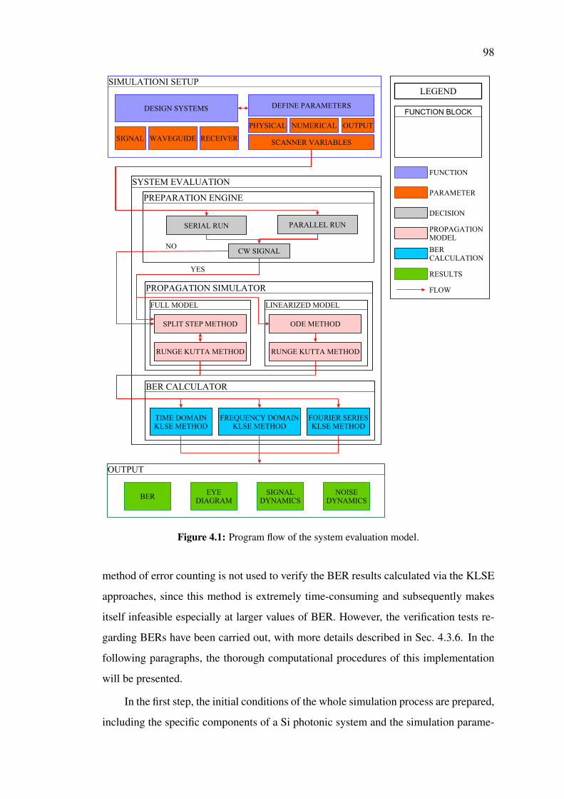
98
Figure 4.1: Program flow of the system evaluation model.
method of error counting is not used to verify the BER results calculated via the KLSE
approaches, since this method is extremely time-consuming and subsequently makes
itself infeasible especially at larger values of BER. However, the verification tests re-
garding BERs have been carried out, with more details described in Sec. 4.3.6. In the
following paragraphs, the thorough computational procedures of this implementation
will be presented.
In the first step, the initial conditions of the whole simulation process are prepared,
including the specific components of a Si photonic system and the simulation parame-
99
ters. To start with, a photonic system can be constructed by defining several groups of
physical parameters illustrated in the first stage of Fig. 4.1: (1) Optical signal parame-
ters. Generally, the signal modulation formats, the central carrier frequency, the signal
power and the bit sequence pattern, as well as the white noise, all have to be properly
selected in order to fulfill the research purpose; (2) Waveguides optical parameters and
dimensions. In particular, the dispersion and nonlinear coefficients of Si waveguides
are required to be calculated. In this dissertation, we obtain the waveguide parameters
of Si-PhWs and Si-PhCWs by using Femsim by Rsoft [13] and MIT Photonic Bands
(MPB) [14], respectively; (3) Receiver schematics. The mathematical expressions will
be given for the direct-detection optical receiver, which contains an band-pass opti-
cal filter, an ideal photodetector and a low-pass electrical filter. As for a M-channel
system, the M sets of optical filters, photodetectors and electrical filters, as well as a
demultiplexer are used in the direct-detection.
Another significant aspect of the simulation setup is the numerical parameters. Ba-
sically, they can be divided into the following groups according to different numerical
algorithms: (1) the temporal sampling points (or FFT points), the distance step and the
time window for the SSFM method and the ODE model; (2) the Cash-Karp parameters
[15] and Dormand-Prince parameters [16] for the fifth-order Runge-Kutta method (see
Appendix. B); (3) the temporal sampling points, bit-rate (or bit interval), weights and
abscissas of Gaussian-Hermite rule for the time-domain KLSE method; (4) the number
of frequency points for both the frequency-domain and Fourier-series KLSE methods.
Moreover, the output parameters determines the types of results. Apart from the es-
sential simulation parameters, we also define the scanner variables. One or more input
parameters can be automatically scanned in the simulation process, such as the signal
power, the pulsewidth, the bit-rate and the waveguide length. Notably, the numerical
parameters are not suggested to be scanned. Since the computational accuracy can only
be ensured by choosing suitable values of these parameters, there is no point to con-
tinue the simulation if this condition can not be satisfied. Importantly, the values of all
the relevant parameters are given in Sec. 4.3.6.
Moving on now to consider the core of the numerical scheme – the system eval-
uation. The system evaluation process is composed of three stages. In particular, the
first stage is the preparation engine. In this stage, two decision operations will be per-
100
formed: one is to choose the types of simulators (or runs), i.e., the serial run and the
parallel run; the other is to identify the shape of the optical signals, namely, CW and
pulse. To be more specific, the parallel run is often employed in the variable scanning,
in order to speed up the whole computational process. The parallel run refers to the
Matlab built-in function par f or [17], where these simulations will be treated as inde-
pendent tasks and then a specific number of tasks will be performed simultaneously.
Additionally, the serial run is adopted in the single simulation operation or the case
where the computational environment (e.g, a single processor) can not support paral-
lel operations. Furthermore, the shape of optical signals decides a specific numerical
routine used in the propagation section, which will be demonstrated in the next stage.
The second stage of the system evaluation engine is the propagation simulator.
Take the case of single-wavelength propagation for instance. Firstly, the optical signals
of Eqs. (2.6) will be placed at the input of Si waveguides. Then, the semi-analytical
solutions regarding the output signals can be derived by using either the full propagation
algorithm (Eqs. (2.15) and (2.20)) or the linearized version ( Eqs. (2.26) and (2.27)).
Precisely, both types of simulators can be selected for the CW signals (uOOK , uPSK),
whereas only the first simulator is capable of simulating the pulsed signal (uG). In case
of the multi-wavelength co-propagation, the analysis is carried out by first extracting
the mathematical expression for signals in each channel (e.g., Eq. (2.28)), and then
modifying the single-channel numerical routines to the multi-channel case by using
Eqs. (2.21) and Eqs. (2.30), (2.31), respectively. Therefore, the explicit numerical
implementation details for full and linearized propagation models will be presented in
Sec. 4.3.1 and Sec. 4.3.2, respectively.
Another important stage is the BER calculator. From Fig. 4.1, we can see that
the time-domain, frequency-domain and Fourier-series KLSE calculators are available
in the BER estimation. The system BERs are determined by Eqs. (3.35), (3.38) and
(3.41). The numerical procedures to implement these calculators will be explained
in Sec. 4.3.3, Sec. 4.3.4 and Sec. 4.3.5. Particularly, the time- and frequency-domain
KLSE calculators are only suitable for CW signals, while the third KLSE calculator
can be applied to all shape of optical signals. At this stage, the numerical discretization
must be carefully performed in order to guarantee the convergence and accuracy. Once
the simulation operation is completed, the whole evaluation will enter the output stage.
101
Last but not least, the output of the whole system evaluation is illustrated in the
final part of Fig. 4.1. Specifically, four important output characteristics will be gen-
erated, namely BER, eye diagrams, signal dynamics and noise dynamics. The BER
results are exported in form of DAT files, and can be viewed via softwares like Matlab
and Python. Moreover, the eye diagrams can be inspected either at the output of optical
filters or at the back-end of the receiver. In addition, the signal dynamics and the noise
dynamics can be exported by utilizing either the propagation simulator or the entire
simulation engine, with the difference existing between the optical dynamics and the
electrical dynamics correspondingly.
4.3 Algorithms in the System Evaluation EngineIn this section, different numerical algorithms employed in the system evaluation en-
gine will be presented. Moreover, the complementary explanation regarding the KLSE
computational routines will be made for the case of multi-channel system performance
analysis.
4.3.1 Full Algorithm of Signal Propagation
The full signal propagation models provide an accurate description for the evolution of
the optical field and FCs in Si waveguides, which incorporate all the essential linear
and nonlinear optical effects, as shown in Sec. 2.6. Note that the theoretical algorithm
of SSFM has been introduced in Sec. 2.8.1. Before proceeding to the SSFM imple-
mentation, it is also important to briefly discuss the choice of time and distance steps.
For convergence, we first choose a specific time and distance steps, and get the result
data. Then we test with smaller values of both steps until the results are matchable
with previous one. Eventually, we will choose certain values for both time and distance
steps according to the computational accuracy and efficiency. In this section, I will first
introduce the numerical procedure to construct full model of the single-wavelength sig-
nal propagation, followed by the implementation of full propagation model with regard
to the multi-wavelength optical signals.
Firstly, the full details of implementing single-channel model numerically are ex-
plained as follows:
1. Obtain the linear operator D and nonlinear operator N in forms of Eq. (2.33a)
102
and Eq. (2.33b), respectively.
2. Choose a distance step h and calculate the optical field at each h. h can be ob-
tained by dividing the transmission distance L into n segments, namely, h = L/n.
Then, the output optical field is computed via Eq. (2.38). Importantly, the calcu-
lation of FCs density is operated in the linear step, where the fifth-order Runge
Kutta method in AppendixB is employed.
3. Record the simulation results in a DAT file.
When compared with the case of single-wavelength signal propagation, the nu-
merical implementation of multi-wavelength signal propagation model requires more
steps:
1. Derive the linear operator Di and nonlinear operator Ni in the i channel (i =
1, ...,M, M is the total number of signal wavelengths), by using Eqs. (2.21a) and
(2.32).
2. Divide the transmission distance L into n segments, with distance step h. Ac-
cording to Eq. (2.38), the linear operator Di will be performed on the electrical
field of the i channel in the frequency domain, during a distance of h/2. Impor-
tantly, this process must be carried out by using a loop, in order to construct the
M coupled NLSE. Then, calculate the overall FCs density at h/2 by applying the
fifth-order Runge Kutta method on Eq. (2.21b).
3. Build a distance loop to derive the semi-analytical solutions for the optical signal
ui at the distance point z j = jh, j = 0, ...,n−1:
(a) Repeat step 2 during a distance from z j to z j +h/2.
(b) Compute the nonlinear operator Ni at z j + h/2, by using the FCs density
calculated from last step. Then multiply the electrical field of the ith channel
with Ni in the time domain, and repeat this operation for the remaining
channels in a loop.
(c) Repeat step 2 during a distance from z j +h/2 to z j+1.
4. Inverse step 2 by using −D, and write the results of each channel in a separate
DAT file.
103
In both procedures mentioned above, the FFT technique is applied for the conversion
of optical signal between frequency-domain and time-domain.
4.3.2 Linearized Algorithm of Signal Propagation
The linearized propagation algorithms are designed for the CW signals, which requires
less computational time but with high accuracy. As mentioned in Sec. 2.7, two as-
sumptions are made for the linearization: one is that the terms containing quadratic
and higher-order noise are discarded under low noise power condition; the other is
that the FC-mediated coefficients αfc and δnFC are assumed to be related to the carrier
density N under this approximation: δnfc = σnN and αfc = σαN, where N is the FC
density, σα = 1.45×10⁻²¹(λ/λ0)2 (in units of m2), and σn = σ(λ/λ0)
2 (in units of
m3), with σ and λ0 = 1550nm being a power dependent coefficient [18] and a reference
wavelength, respectively. Two numerical routines regarding the linearized propagation
models will be described in this section.
The first numerical routine is developed for the single-channel CW signal propa-
gation. This routine works for both the OOK modulated CW signal (Φ0 = 0) and the
PSK modulated CW signal. The main steps are listed as follows:
1. Recast Eqs. (2.26) and (2.27) in forms of Eqs. (2.41), where A = P, B = Φ,
C = A′ and D = A′′. Then implement these ODEs in a Matlab function.
2. Obtain the initial conditions of input field y0 = [A0;B0;C0;D0] and distance steps
tspan = [t0, t1, t2, · · · , t f ].
3. Use the Matlab function ode45 to compute the optical field evolution.
4. Write the output data in a DAT file, including signal power, global phase, in-
phase and quadrature noise components.
Furthermore, the second routine is designed for the multi-wavelength signal co-
propagation. The formulae of the multi-wavelength OOK optical signal propagation
are given in Sec. 2.7.2. It is important to mention that these mathematical expressions
are ODEs. Therefore, the computational procedure regarding M-wavelength linearized
model is illustrated below:
104
1. Derive the M coupled ODEs from Eqs. (2.30) and (2.31), and write up the cor-
responding Matlab functions. As an expansion of the single-channel CW signal
case, these functions are organized by a loop, with the iteration number equaling
to the total channel number. Inside of this loop, the numerical operations are the
same as the numerical implementations for single-channel CW signal case. Note
also that the coefficients of these ODEs have to be calculated simultaneously
inside the loop.
2. Perform the Matlab function ode45 on the functions obtained from Step 1, and
use the initial conditions, which contain the M-channel input field, distance steps
and total channel number.
3. Record the results of signal power, global phase, in-phase and quadrature noise
components in a DAT file, for all channels.
Numerical tests shows that this algorithm has good agreement with the full propagation
models.
4.3.3 Time-domain KLSE Algorithm in BER Calculation
The computational algorithm of the time-domain KLSE method is illustrated here to
evaluate the transmission BER in Si waveguides. Implemented as the Matlab codes,
this numerical routine is relatively simple to construct, due to its logic consistency.
However, the difficult part of the time-domain method is the derivation of the noise
correlation matrix at output of the receiver. The whole process regarding the noisy CW
signal transmission and detection are briefly summarized below:
1. Run the main simulation loop for the noisy signal propagation in the Si waveg-
uides.
(a) Setup the essential simulation condition by loading a input file which in-
cludes all necessary physical and numerical parameters, namely, the signal
properties (e.g., input power, bit sequence and pulsewidth), the waveguide
linear and nonlinear optical parameters, as well as the computational time
window, FFT points and distance step;
(b) Use either the SSFM demonstrated in Sec. 4.3.1 or the ODEs solvers pre-
sented in Sec. 4.3.2 to derive the output signal from the waveguides.
105
2. Calculate the receiver-output noise correlation matrix in the time-domain, and
compute the new signal-related variable.
(a) Separate the noise and signal at the input of the receiver;
(b) Calculate the noise correlation matrix before and after the optical receiver,
by applying Eqs. (3.2) and (3.3);
(c) Apply the Gauss-Hermite technique by deriving the explicit formulas for
Eqs. (A.2), (A.3) and (A.4), and then obtain the correlation matrix at the
end of the receiver according to Eq. (3.11);
(d) Expand the signal and complex noise components after the optical filter in
form of Eqs. (3.5), and use the relevant expansion coefficients, skα, pk
α,
and qkα to construct new vector variables sk and nk.
3. Compute the system BER according to the time-domain noise correlation matrix
and the related MGF:
(a) Diagonalize the correlation matrix by using Eq. (3.13), and recast the signal
vector in new form of Eq. (3.15a);
(b) Derive the MGF function format based on Eq. (3.16);
(c) Calculate BER by applying the saddle-point approximation in Sec. 3.5 on
the MGF function via Eqs. (3.35) and (3.38);
(d) Record the BER in a DAT file.
With regard to the multi-channel system, the computational process is quite similar
to the algorithm mentioned above. However, there are two major difference between
the multi-channel and single-channel numerical implementation. One is that the input
files, the SSFM simulator and the ODEs simulator in Step 1 all have to be switched to
the multi-channel case. In addition, the signal detection (Step 2 and Step 3) is applied in
each receiver that corresponds to one independent channel, and then the overall system
BER is calculated by averaging the BER from each channel. This implementation is
reasonable, due to the fact that the functionality of a demultiplexer in our model is
to separate the signals with different wavelength, but without inducing any electrical
noise.
106
4.3.4 Frequency-domain KLSE Algorithm in BER Calculation
Similar to the time-domain KLSE routine, the full computational algorithm of the
frequency-domain KLSE method is also implemented in Matlab. Moreover, this al-
gorithm is focused on the noisy CW signal as well. In particular, the frequency-domain
KLSE is numerically easy to be extended to other applications, such as WDM systems
and the optical systems that employ advanced modulation formats. The numerical pro-
cess for the frequency-domain KLSE is described below:
1. Start a simulation loop for the signal transmission, similar to the first step in
Sec. 4.3.3. Here, we need to specify a new central frequency points 2Q+ 1 for
the noisy signal.
2. Simulate the receiver-output noise correlation matrix in the frequency domain,
and compute the related phase-shifted signal variable.
(a) Derive the photocurrent at the end of the receiver and the related Hermitian
kernal, in forms of Eqs. (3.17) and (3.18), repsectively;
(b) Discretize the Hermitian kernel and then multiply the with frequency step
δ f , yielding new forms of the receiver matrix and the electrical field, as
well as the photocurrent that is expressed as Eqs. (3.19);
(c) Rewrite the receiver matrix and the electrical field into real-valued matrixes.
(d) Compute the correlation matrix in frequency-domain by applying
Eqs. (3.20), (3.21) and (3.22);
3. Compute the final BER by deriving the noise correlation matrix in frequency-
domain and further the MGF:
(a) Derive the eigenfunction and eigenvalues by using an orthogonal matrix to
diagonalize the noise correlation matrix at the receiver output, according to
Eq. (3.23);
(b) Calculate the phase-shift signal vector by using the expansion in
Eq. (3.24b);
(c) Compute the MGF by using Eq. (3.26);
107
(d) Derive the transmission BER by using the saddle-point approximation on
the MGF, obtaining Eqs. (3.35) and (3.41), as illustrated in Sec. 3.5;
(e) Save all the BER results in an easily-traceable file.
As was pointed out in Sec. 4.3.3, there are also two changes in the numerical
scheme for the multi-channel system analysis in the frequency domain, when compared
with the single-channel case. Therefore, the corresponding implementation regarding
multi-channel systems in frequency domain can refer to the last paragraph in Sec. 4.3.3.
4.3.5 Fourier-series KLSE Algorithm in BER Calculation
The numerical calculations of the PDFs for Signal “1” and Signal “0” can also be done
by using the Fourier-series KLSE method in combination with the perturbation theory.
Specifically, the optical signal propagation in Si waveguides and the followed BER
detection and calculation are all implemented in Matlab. The implementation routine
for the single-channel systems is presented as follows:
1. Setup a main simulation process for the noise-free optical signal (s0(t,0)) trans-
mission in Si waveguides:
(a) Read a input file with initial conditions for all necessary physical and nu-
merical parameters;
(b) Run the SSFM numerical simulator according to Sec. 4.3.1. Then obtain
the output signal in the central channel as s0(t,L), and save it.
2. Calculate the noise correlation matrix at the end of the Si waveguide. To start
with, compute the correlation matrix Rk(0) based on the input complex white
noise, with the matrix dimension of (4Q+ 2)× (4Q+ 2). After obtaining the
noise free signal s0(t,L) in the central channel at z = L, we then continue with
the simulation process for different input signal in the same channel:
(a) Obtain sβ (t,0) by perturbing s0(t,0) in the β -th frequency mode with
an extremely small amount ∆, in correspondence to Eq. (3.28). Here,
β = 1, ...,(2Q+ 1), (2Q+ 1) is the chosen frequency points in the central
part of signal spectrum. Particularly, we use two values of ∆ in the signal
initialization, which are a real positive number and an imaginary positive

108
number for the same 1 to (2Q+ 1) frequency components. Then launch
sβ (t,0) at input of the Si waveguide;
(b) Calculate the waveguide output signal sβ (t,L) by solving Eqs. (2.15) and
(2.20);
(c) Compute δ sβ (t) = sβ (t,L)− s0(t,L) and its Fourier coefficients, wβ ;
(d) Find the (4Q+ 2)× (2Q+ 1) transmission matrix R by using Eq. (3.29).
Then recast R into a (4Q+2)× (4Q+2) real-valued matrix.
(e) Obtain the noise correlation matrix after transmission according to
Eq. (3.27).
3. Computation of the System BER based on the Noise Correlation Matrix:
(a) Read the output noise-free signal and transfer it into the frequency domain.
And then load the noise correlation matrix at the output of Si waveguide,
Rk.
(b) Calculate the real receiver matrix W from W = [D ′,−D ′′;D ′′,D ′], where
D is a Hermitian kernel.
(c) Diagonalize the combined matrix of the Rk(L) and W ;
(d) Calculate the signal shift variable χq based on Eqs. (3.31), (3.32) and
(3.33);
(e) Compute the MGF function from Eq. (3.34);
(f) Calculate BER by performing the saddle-point approximation presented in
Sec. 3.5 on the MGF, referring to Eqs. (3.35) and (3.41);
(g) Save BER and write them into a recorded file.
Importantly, the correlation matrix calculation in multi-channel systems are slight
different from that of single-channel systems. The basic idea is to compute only the
noise correlation matrix in the central channel, by perturbing the signal in the central
channel and leaving the other channels to be noise free. It has been verified that the
cross correlation between the noise in the investigated channel and the noise from the
rest channels can be neglected, when compared with noise correlation in the central
channel. The remaining part of BER calculation is identical to that of single-channel.
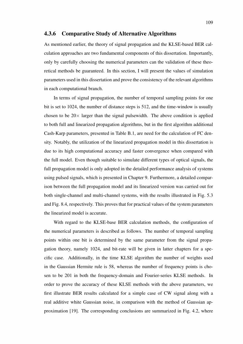
109
4.3.6 Comparative Study of Alternative Algorithms
As mentioned earlier, the theory of signal propagation and the KLSE-based BER cal-
culation approaches are two fundamental components of this dissertation. Importantly,
only by carefully choosing the numerical parameters can the validation of these theo-
retical methods be guaranteed. In this section, I will present the values of simulation
parameters used in this dissertation and prove the consistency of the relevant algorithms
in each computational branch.
In terms of signal propagation, the number of temporal sampling points for one
bit is set to 1024, the number of distance steps is 512, and the time-window is usually
chosen to be 20× larger than the signal pulsewidth. The above condition is applied
to both full and linearized propagation algorithms, but in the first algorithm additional
Cash-Karp parameters, presented in Table B.1, are need for the calculation of FC den-
sity. Notably, the utilization of the linearized propagation model in this dissertation is
due to its high computational accuracy and faster convergence when compared with
the full model. Even though suitable to simulate different types of optical signals, the
full propagation model is only adopted in the detailed performance analysis of systems
using pulsed signals, which is presented in Chapter 9. Furthermore, a detailed compar-
ison between the full propagation model and its linearized version was carried out for
both single-channel and multi-channel systems, with the results illustrated in Fig. 5.3
and Fig. 8.4, respectively. This proves that for practical values of the system parameters
the linearized model is accurate.
With regard to the KLSE-base BER calculation methods, the configuration of
the numerical parameters is described as follows. The number of temporal sampling
points within one bit is determined by the same parameter from the signal propa-
gation theory, namely 1024, and bit-rate will be given in latter chapters for a spe-
cific case. Additionally, in the time KLSE algorithm the number of weights used
in the Gaussian Hermite rule is 58, whereas the number of frequency points is cho-
sen to be 201 in both the frequency-domain and Fourier-series KLSE methods. In
order to prove the accuracy of these KLSE methods with the above parameters, we
first illustrate BER results calculated for a simple case of CW signal along with a
real additive white Gaussian noise, in comparison with the method of Gaussian ap-
proximation [19]. The corresponding conclusions are summarized in Fig. 4.2, where
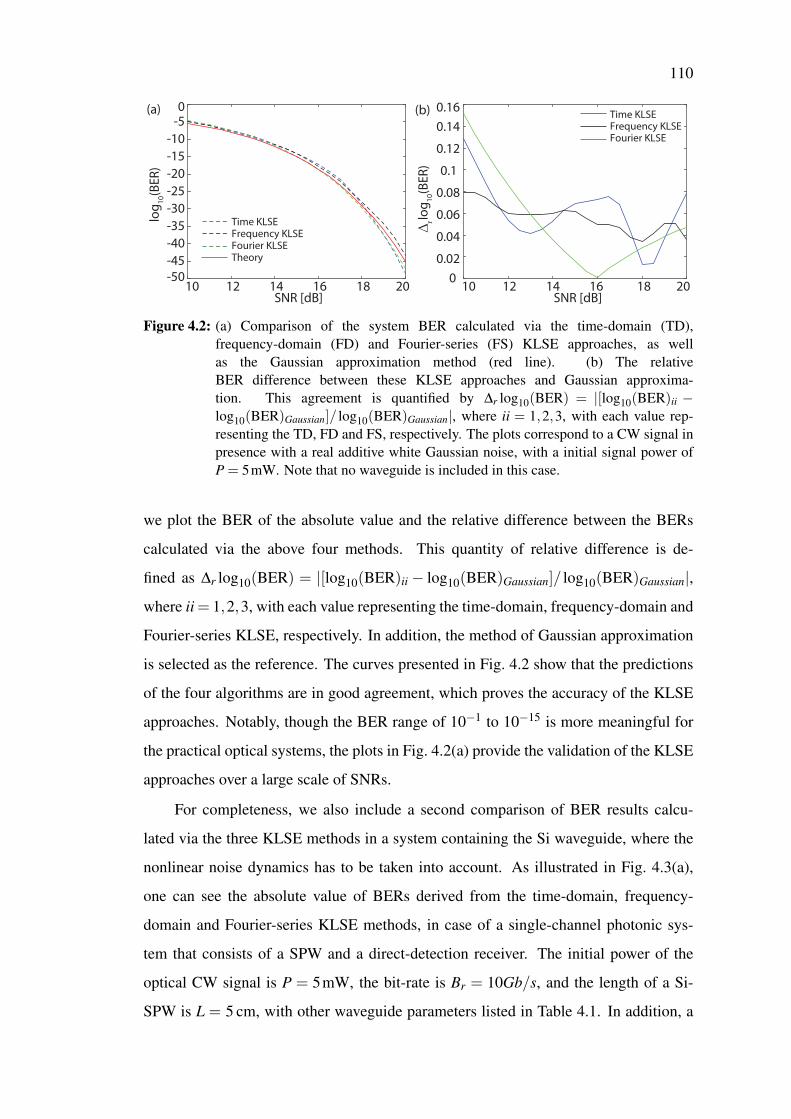
110
00.02
0.04
0.06
0.08
0.1
0.12
0.140.16
∆ rlo
g 10(B
ER)
(b)
Time KLSEFrequency KLSEFourier KLSETheory
-50-45-40-35-30-25-20-15-10
-50
log 10
(BER
)
(a)
10 12 14 16 18 20SNR [dB]
Time KLSEFrequency KLSEFourier KLSE
10 12 14 16 18 20SNR [dB]
Figure 4.2: (a) Comparison of the system BER calculated via the time-domain (TD),frequency-domain (FD) and Fourier-series (FS) KLSE approaches, as wellas the Gaussian approximation method (red line). (b) The relativeBER difference between these KLSE approaches and Gaussian approxima-tion. This agreement is quantified by ∆r log10(BER) = |[log10(BER)ii −log10(BER)Gaussian]/ log10(BER)Gaussian|, where ii = 1,2,3, with each value rep-resenting the TD, FD and FS, respectively. The plots correspond to a CW signal inpresence with a real additive white Gaussian noise, with a initial signal power ofP = 5mW. Note that no waveguide is included in this case.
we plot the BER of the absolute value and the relative difference between the BERs
calculated via the above four methods. This quantity of relative difference is de-
fined as ∆r log10(BER) = |[log10(BER)ii − log10(BER)Gaussian]/ log10(BER)Gaussian|,
where ii= 1,2,3, with each value representing the time-domain, frequency-domain and
Fourier-series KLSE, respectively. In addition, the method of Gaussian approximation
is selected as the reference. The curves presented in Fig. 4.2 show that the predictions
of the four algorithms are in good agreement, which proves the accuracy of the KLSE
approaches. Notably, though the BER range of 10−1 to 10−15 is more meaningful for
the practical optical systems, the plots in Fig. 4.2(a) provide the validation of the KLSE
approaches over a large scale of SNRs.
For completeness, we also include a second comparison of BER results calcu-
lated via the three KLSE methods in a system containing the Si waveguide, where the
nonlinear noise dynamics has to be taken into account. As illustrated in Fig. 4.3(a),
one can see the absolute value of BERs derived from the time-domain, frequency-
domain and Fourier-series KLSE methods, in case of a single-channel photonic sys-
tem that consists of a SPW and a direct-detection receiver. The initial power of the
optical CW signal is P = 5mW, the bit-rate is Br = 10Gb/s, and the length of a Si-
SPW is L = 5 cm, with other waveguide parameters listed in Table 4.1. In addition, a
111
10 12 14 16 18 20SNR[dB]
-45-40-35-30-25
-20-15
-10
-50
10 12 14 16 18 20SNR[dB]
0
0.02
0.04
0.06
0.08
0.1
0.12
0.14
∆ rlo
g 10(B
ER)
log 10
(BER
)
(a) (b)
Time KLSEFrequency KLSEFourier KLSE
Time KLSEFourier KLSE
Figure 4.3: (a) Comparison of the system BER calculated via the time-domain (TD),frequency-domain (FD) and Fourier-series (FS) KLSE approaches. (b) The rel-ative BER difference between the frequency-domain KLSE and the other twoKLSE emthods. This agreement is quantified by ∆r log10(BER) = |[log10(BER)ii−log10(BER)FD]/ log10(BER)FD|, where ii = 1,2, with each value representing theTD and FS, respectively. The plots correspond to a single-channel Si-PhW systemusing a NRZ CW signal together with a complex additive white Gaussian noise.The initial power of the CW signal is P = 5mW, Br = 10Gb/s, L = 5 cm and theother waveguide parameters is illustrated in Table 4.1.
vivider picture about the difference of these three KLSE methods is shown in Fig. 4.3
(b), where the evaluation quantity is denoted as ∆r log10(BER) = |[log10(BER)ii −
log10(BER)FD]/ log10(BER)FD|, where ii= 1,2, with each value representing the time-
domain and Fourier-series KLSE, respectively. Here, the frequency-domain KLSE is
selected as the reference. To conclude, these curves in Fig. 4.3 suggest that the time-
domain, frequency-domain, and Fourier-series KLSE methods are matching with each
other very well, which in turn ensures the accuracy of simulation results in the latter
chapters.
Table 4.1: Main parameters for a Si-PhW used in Fig. 4.3.
w [nm] h [nm] λ [nm] β2 [ps2 m−1] κ γ ′ [W−1 m−1] γ ′′ [W−1 m−1]900 250 1550 0.54 0.9685 166.8403 50.8236
Last but not least, we also validate the accuracy of the KLSE methods in multi-
channel photonic systems. Thus, another comparison of BERs calculated by employ-
ing the time- and frequency-domain methods for three different 8-channel Si photonic
systems is presented in Fig. 8.6. The information that conveys in Fig. 8.6 strength-
ens the idea that these two KLSE algorithms are in agreement with each other. As
stated earlier, the Fourier-series KLSE method is only utilized for the single-channel
112
performance analysis in this dissertation, which is the reason why this algorithm is not
included in the multi-channel BER comparison.
4.4 ConclusionsIn this chapter, the computational implementation details of the entire system evalu-
ation model is discussed. This numerical tool can support not only accurate investi-
gations of the signal propagation in Si waveguides, but also precise evaluation of the
overall system performance. Moreover, the current numerical algorithms are also of ex-
cellent expandability, which can be applied in other optical devices and more sophisti-
cated photonic systems. To our knowledge, this is the first time to provide the complete
numerical implementation of the linearized propagation models for Si waveguides.
113
Bibliography[1] Matlab version R2016b, https://uk.mathworks.com/products/matlab.html.
[2] G. P. Agrawal, Nonlinear Fiber Optics 4th ed., (Academic Press, 2006).
[3] J. N. Reddy, An introduction to the finite element method, (New York: McGraw-
Hill, 1993).
[4] A. Taflove and S. Hagness, Computational Electrodynamics, The finite-difference
time-domain method, 3rd ed., (Artech House, 2005).
[5] D. F. G. Gallagher and T. P. Felici, “Eigenmode Expansion Method for Simulation
of Optical Propgation in Photonics - Pros and Cons,” Proc. SPIE 4987, 69-82
(2003).
[6] L. Wang, and S.I. Rokhlin, “Stable reformulation of transfer matrix method for
wave propagation in layered anisotropic media,” Ultrasonics 39, 413-424 (2001).
[7] K. Okamoto, Fundamentals of optical waveguides, (Academic press, 2010).
[8] A. Carena, V. Curri, R. Gaudino, P. Poggiolini, and S. Benedetto. “A time-domain
optical transmission system simulation package accounting for nonlinear and
polarization-related effects in fiber,” IEEE J. Sel. Areas Commun. 15, 751-765
(1997).
[9] SSPROP, develped by Ross Pleban (NCSU), Afrouz Azari (UMD), Reza Salem
(UMD) and T. E. Murphy (UMD). http://www.photonics.umd.edu/
software/ssprop/.
[10] SIMFOCS, developed by Dr. Siegfried Geckeler, Horwitzstr.1, D-81739
Munich, Germany. http://www.geckeler.homepage.t-online.de/
simfocs/smfe.htm.
[11] Rsoft Design Group, Optsim, https://optics.synopsys.com/rsoft/
rsoft-system-network-optsim.html.
[12] PHOTOSS, http://www.lenge.de/english/.
114
[13] Rsoft Design Group, Femsim, https://optics.synopsys.com/
rsoft/rsoft-passive-device-femsim.html.
[14] MIT Photoinc Bands, http://ab-initio.mit.edu/wiki/index.
php/MIT_Photonic_Bands.
[15] W. H. Press, S. A. Teukolsky, W. T. Vetterling, and B. P. Flannery, “Numerical
Receipes in C: The Art of Scientific Computing,” Cambridge University Press
(1992).
[16] J. R. Dormand, and P. J. Prince, “A family of embedded Runge-Kutta formulae,”
J. Computational and Applied Mathsmatics 6, 19-26 (1980).
[17] Matlab version R2016b, PARFOR, https://uk.mathworks.com/help/
distcomp/parfor.html.
[18] Q. Lin, O. J. Painter, and G. P. Agrawal, “Nonlinear optical phenomena in silicon
waveguides: Modeling and applications,” Opt. Express 15, 16604-16644 (2007).
[19] P. Sun, M. M. Hayat, B. E. A. Saleh, and M. C. Teich, “Statistical correlation of
gain and buildup time in APDs and its effects on receiver performance,” IEEE J.
Lightwave Technol. 24, 755-768 (2006).
Chapter 5
Calculation of Bit Error Rates in
Optical Systems with Strip Silicon
Photonic Wires
5.1 IntroductionIn this chapter, we perform a theoretical analysis of the transmission BER in a system
consisting of a Si-PhW linked with a direct-detection optical receiver containing an
optical filter, an ideal square-law photodetector, and an electrical filter (see Fig. 5.1).
We assume that the bandwidth of the optical filter is larger than the bit rate of the
optical signal, whereas the bandwidth of the electrical filter is close to the bit rate. In
particular, an integrate-and-dump electrical filter is employed in this work, which can
be viewed as a matched filter for the nonreturn-to-zero (NRZ) signals. At the front-end
of the system the optical field is assumed to be a superposition of an ON-OFF keying
(OOK) modulated NRZ optical signal, with ON and OFF power values of P0 and zero,
respectively, and a stationary additive white Gaussian noise containing an in-phase and
a quadrature component. For simplicity, we assume that these two noise components
are uncorrelated, a constraint that can be easily relaxed if needed. To describe the
optical field propagation in the Si-PhW we use a rigorous model [1] that incorporates
linear and nonlinear optical effects, including free-carrier (FC) dispersion (FCD), FC
absorption (FCA), self-phase modulation (SPM), and two-photon absorption (TPA), as
well as the FCs dynamics and the interaction between the FCs and the optical field.
A linearized system governing the optical noise dynamics in the presence of FCs is
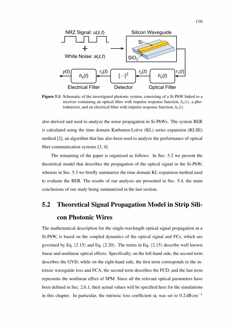
116
Silicon Waveguide
∙ 2
Detector
NRZ Signal: u(z,t)
White Noise: a(z,t)
y(t)
SiO2
Electrical Filter Optical Filter
r3(t) r1(t)r2(t)he(t) ho(t)
Si
Figure 5.1: Schematic of the investigated photonic system, consisting of a Si-PhW linked to areceiver containing an optical filter with impulse response function, ho(t), a pho-todetector, and an electrical filter with impulse response function, he(t).
also derived and used to analyze the noise propagation in Si-PhWs. The system BER
is calculated using the time domain Karhunen-Loeve (KL) series expansion (KLSE)
method [2], an algorithm that has also been used to analyze the performance of optical
fiber communication systems [3, 4].
The remaining of the paper is organized as follows. In Sec. 5.2 we present the
theoretical model that describes the propagation of the optical signal in the Si-PhW,
whereas in Sec. 5.3 we briefly summarize the time domain KL expansion method used
to evaluate the BER. The results of our analysis are presented in Sec. 5.4, the main
conclusions of our study being summarized in the last section.
5.2 Theoretical Signal Propagation Model in Strip Sili-
con Photonic WiresThe mathematical description for the single-wavlength optical signal propagation in a
Si-PhW, is based on the coupled dynamics of the optical signal and FCs, which are
governed by Eq. (2.15) and Eq. (2.20). The terms in Eq. (2.15) describe well known
linear and nonlinear optical effects. Specifically, on the left-hand side, the second term
describes the GVD, while on the right-hand side, the first term corresponds to the in-
trinsic waveguide loss and FCA, the second term describes the FCD, and the last term
represents the nonlinear effect of SPM. Since all the relevant optical parameters have
been defined in Sec. 2.6.1, their actual values will be specified here for the simulations
in this chapter. In particular, the intrinsic loss coefficient αi was set to 0.2 dBcm−1
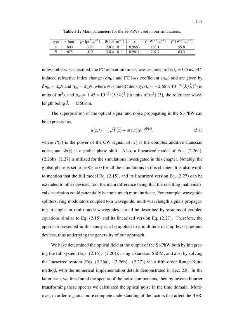
117
Table 5.1: Main parameters for the Si-PhWs used in our simulations.
Type w [nm] β2 [ps2 m−1] β3 [ps3 m−1] κ γ ′ [W−1 m−1] γ ′′ [W−1 m−1]A 800 0.26 2.8×10⁻³ 0.9663 183.1 55.8B 675 -0.2 3.8×10⁻³ 0.9611 207.7 63.3
unless otherwise specified, the FC relaxation time tc was assumed to be tc = 0.5 ns, FC-
induced refractive index change (δnfc) and FC loss coefficient (αfc) and are given by
δnfc = σnN and αfc = σαN, where N is the FC density, σn =−2.68×10⁻²⁶(λ/λ )2 (in
units of m3), and σα = 1.45×10⁻²¹(λ/λ )2 (in units of m2) [5], the reference wave-
length being λ = 1550 nm.
The superposition of the optical signal and noise propagating in the Si-PhW can
be expressed as,
u(z, t) = [√
P(z)+a(z, t)]e− jΦ(z), (5.1)
where P(z) is the power of the CW signal, a(z, t) is the complex additive Gaussian
noise, and Φ(z) is a global phase shift. Also, a linearized model of Eqs. (2.26a),
(2.26b) (2.27) is utilized for the simulations investigated in this chapter. Notably, the
global phase is set to be Φ0 = 0 for all the simulations in this chapter. It is also worth
to mention that the full model Eq. (2.15), and its linearized version Eq. (2.27) can be
extended to other devices, too, the main difference being that the resulting mathemati-
cal description could potentially become much more intricate. For example, waveguide
splitters, ring modulators coupled to a waveguide, multi-wavelength signals propagat-
ing in single- or multi-mode waveguides can all be described by systems of coupled
equations similar to Eq. (2.15) and its linearized version Eq. (2.27). Therefore, the
approach presented in this study can be applied to a multitude of chip-level photonic
devices, thus underlying the generality of our approach.
We have determined the optical field at the output of the Si-PhW both by integrat-
ing the full system (Eqs. (2.15), (2.20)), using a standard SSFM, and also by solving
the linearized system (Eqs. (2.26a), (2.26b), (2.27)) via a fifth-order Runge-Kutta
method, with the numerical implementation details demonstrated in Sec. 2.8. In the
latter case, we first found the spectra of the noise components, then by inverse Fourier
transforming these spectra we calculated the optical noise in the time domain. More-
over, in order to gain a more complete understanding of the factors that affect the BER,
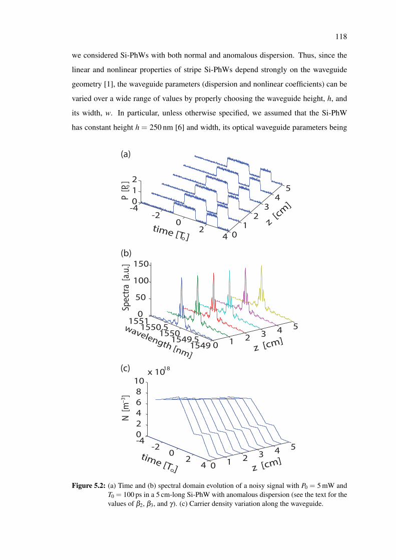
118
we considered Si-PhWs with both normal and anomalous dispersion. Thus, since the
linear and nonlinear properties of stripe Si-PhWs depend strongly on the waveguide
geometry [1], the waveguide parameters (dispersion and nonlinear coefficients) can be
varied over a wide range of values by properly choosing the waveguide height, h, and
its width, w. In particular, unless otherwise specified, we assumed that the Si-PhW
has constant height h = 250 nm [6] and width, its optical waveguide parameters being
0 1 2 3 4 5
15491549.5
15501550.5
15510
50
100
150
z [cm]
wavelength [nm]
Spec
tra
[a.u
.]
(b)
0 1 2 3 4 5
4 2
0-2
-40
2
4
6
8
10x 10
18
z [cm]time [T
o]
N [
m−
3]
(c)
01
23
45
42
0-2
-40
1
2
z [cm
]
time [To]
P [
P o]
(a)
Figure 5.2: (a) Time and (b) spectral domain evolution of a noisy signal with P0 = 5 mW andT0 = 100 ps in a 5 cm-long Si-PhW with anomalous dispersion (see the text for thevalues of β2, β3, and γ). (c) Carrier density variation along the waveguide.
119
thus independent of the distance along the waveguide, z. By adjusting the width w of
Si-PhWs, it can be easily achieved the switch from the normal dispersion region to the
anomalous dispersion. The main waveguide parameters are listed in Table 5.1.
An example of time and wavelength domain evolution of a noisy signal in a 5 cm-
long Si-PhW with anomalous dispersion is shown in Fig. 5.2, the bit sequence being
“01011000”. For completeness, we also show in Fig. 5.2(c) the dynamics of the pho-
togenerated FCs. It can be seen that the optical field is fairly weakly distorted during
propagation, which means that for the optical power considered in these simulations
the nonlinear effects are small. The most notable feature revealed by these plots is the
signal decay, which is due to the intrinsic losses, FCA, and TPA. The generation of the
FCs that produce FCA is illustrated in Fig. 5.2(c), where the increase in the FC density
induced by each “1”-bit can be clearly seen.
In order to determine the accuracy with which the linearized system (Eq. (2.26))
describes the propagation of the optical field in the Si-PhW, we calculated the signal
and noise at the back-end of the waveguide by using both the linearized model and full
system Eqs. (2.15), (2.20). The conclusions of this analysis, summarized in Fig. 5.3,
suggest that the linearized system describes fairly accurately the dynamics of the CW
signal and noise, especially when the noise power is small. Thus, Figs. 5.3(b) and
5.3(c) show that both models predict a larger parametric amplification of the quadrature
noise (a finding also supported by the power spectral densities of the two noises, not
shown here) and similar values of the average phase, ϑ , of the noise, which is equal
to the slope of the red lines in these plots. This is a known effect, a larger parametric
gain amplification of the quadrature noise being observed in optical fiber systems, too
[7]. In the case when the linearized system was used, the phase ϑ was calculated
from the relation, ϑ = Earg[a(z, t)], where E· denotes the statistical expectation
operator. When the full system was used, the CW signal parameters were extracted
from the relation,√
P(z)e− jΦ(z) =Eu(z, t), and then the noise was found as a(z, t) =
[u(z, t)−Eu(z, t)]e jΦ(z). Note that in Figs. 5.3(b) and 5.3(c) we plot a(z, t)e− jΦ(z),
calculated at z = L = 5 cm.
A good agreement between the two models can also be observed in their predic-
tions of the dependence of the CW signal power and phase on the distance, z, as per
Fig. 5.3(d). Expectedly, the differences between the results inferred from the two mod-
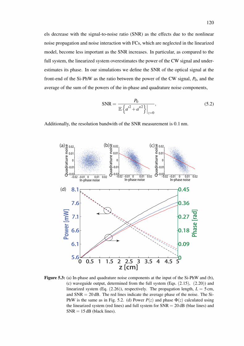
120
els decrease with the signal-to-noise ratio (SNR) as the effects due to the nonlinear
noise propagation and noise interaction with FCs, which are neglected in the linearized
model, become less important as the SNR increases. In particular, as compared to the
full system, the linearized system overestimates the power of the CW signal and under-
estimates its phase. In our simulations we define the SNR of the optical signal at the
front-end of the Si-PhW as the ratio between the power of the CW signal, P0, and the
average of the sum of the powers of the in-phase and quadrature noise components,
SNR =P0
E
a′2 +a′′2∣∣∣
z=0
, (5.2)
Additionally, the resolution bandwith of the SNR measurement is 0.1 nm.
5.6
6.1
6.6
7.1
7.6
8.1
Power [m
W]
z [cm]0 0.5 1 1.5 2 2.5 3 3.5 4 4.5 5
0
0.09
0.18
0.27
0.36
0.45Ph
ase [ra
d]
−0.02 −0.01 0 0.01 0.02−0.02
−0.01
0
0.01
0.02
In-phase noise
Quad
rature noise
−0.02 −0.01 0 0.01 0.02−0.02
−0.01
0
0.01
0.02
In-phase noise
Quad
rature noise
−0.02 −0.01 0 0.01 0.02−0.02
−0.01
0
0.01
0.02
In-phase noise
Quad
rature noise(a) (b) (c)
(d)
Figure 5.3: (a) In-phase and quadrature noise components at the input of the Si-PhW and (b),(c) waveguide output, determined from the full system (Eqs. (2.15), (2.20)) andlinearized system (Eq. (2.26)), respectively. The propagation length, L = 5 cm,and SNR = 20 dB. The red lines indicate the average phase of the noise. The Si-PhW is the same as in Fig. 5.2. (d) Power P(z) and phase Φ(z) calculated usingthe linearized system (red lines) and full system for SNR = 20 dB (blue lines) andSNR = 15 dB (black lines).
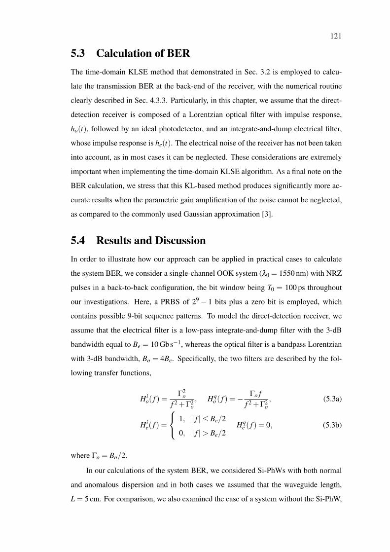
121
5.3 Calculation of BERThe time-domain KLSE method that demonstrated in Sec. 3.2 is employed to calcu-
late the transmission BER at the back-end of the receiver, with the numerical routine
clearly described in Sec. 4.3.3. Particularly, in this chapter, we assume that the direct-
detection receiver is composed of a Lorentzian optical filter with impulse response,
ho(t), followed by an ideal photodetector, and an integrate-and-dump electrical filter,
whose impulse response is he(t). The electrical noise of the receiver has not been taken
into account, as in most cases it can be neglected. These considerations are extremely
important when implementing the time-domain KLSE algorithm. As a final note on the
BER calculation, we stress that this KL-based method produces significantly more ac-
curate results when the parametric gain amplification of the noise cannot be neglected,
as compared to the commonly used Gaussian approximation [3].
5.4 Results and DiscussionIn order to illustrate how our approach can be applied in practical cases to calculate
the system BER, we consider a single-channel OOK system (λ0 = 1550 nm) with NRZ
pulses in a back-to-back configuration, the bit window being T0 = 100 ps throughout
our investigations. Here, a PRBS of 29− 1 bits plus a zero bit is employed, which
contains possible 9-bit sequence patterns. To model the direct-detection receiver, we
assume that the electrical filter is a low-pass integrate-and-dump filter with the 3-dB
bandwidth equal to Be = 10 Gbs−1, whereas the optical filter is a bandpass Lorentzian
with 3-dB bandwidth, Bo = 4Be. Specifically, the two filters are described by the fol-
lowing transfer functions,
H io( f ) =
Γ2o
f 2 +Γ2o, Hq
o ( f ) =− Γo ff 2 +Γ2
o, (5.3a)
H ie( f ) =
1, | f | ≤ Be/2
0, | f |> Be/2Hq
e ( f ) = 0, (5.3b)
where Γo = Bo/2.
In our calculations of the system BER, we considered Si-PhWs with both normal
and anomalous dispersion and in both cases we assumed that the waveguide length,
L = 5 cm. For comparison, we also examined the case of a system without the Si-PhW,
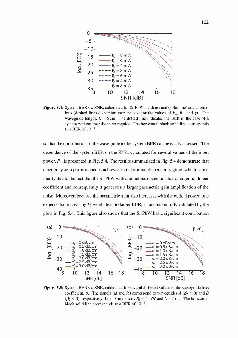
122
8 10 12 14 16 18−35
−30
−25
−20
−15
−10
−5
0
SNR [dB]
log 1
0 (BER)
P0 = 8 mW
P0 = 6 mW
P0 = 4 mW
P0 = 8 mW
P0 = 6 mW
P0 = 4 mW
P0 = 8 mW
Figure 5.4: System BER vs. SNR, calculated for Si-PhWs with normal (solid line) and anoma-lous (dashed line) dispersion (see the text for the values of β2, β3, and γ). Thewaveguide length, L = 5 cm. The dotted line indicates the BER in the case of asystem without the silicon waveguide. The horizontal black solid line correspondsto a BER of 10−9.
so that the contribution of the waveguide to the system BER can be easily assessed. The
dependence of the system BER on the SNR, calculated for several values of the input
power, P0, is presented in Fig. 5.4. The results summarized in Fig. 5.4 demonstrate that
a better system performance is achieved in the normal dispersion regime, which is pri-
marily due to the fact that the Si-PhW with anomalous dispersion has a larger nonlinear
coefficient and consequently it generates a larger parametric gain amplification of the
noise. Moreover, because the parametric gain also increases with the optical power, one
expects that increasing P0 would lead to larger BER, a conclusion fully validated by the
plots in Fig. 5.4. This figure also shows that the Si-PhW has a significant contribution
8 10 12 14 16 18−40
−30
−20
−10
0
SNR [dB]
log10(BER)
αi = 0 dB/cm
αi = 0.5 dB/cm
αi = 1.0 dB/cm
αi = 1.5 dB/cm
αi = 2.0 dB/cm
αi = 2.5 dB/cm
αi = 3.0 dB/cm
(a) β2>0
8 10 12 14 16 18−40
−30
−20
−10
0
SNR [dB]
αi = 0 dB/cm
αi = 0.5 dB/cm
αi = 1.0 dB/cm
αi = 1.5 dB/cm
αi = 2.0 dB/cm
αi = 2.5 dB/cm
αi = 3.0 dB/cm
(b) β2<0
log10(BER)
Figure 5.5: System BER vs. SNR, calculated for several different values of the waveguide losscoefficient, αi. The panels (a) and (b) correspond to waveguides A (β2 > 0) and B(β2 < 0), respectively. In all simulations P0 = 5 mW and L = 5 cm. The horizontalblack solid line corresponds to a BER of 10−9.
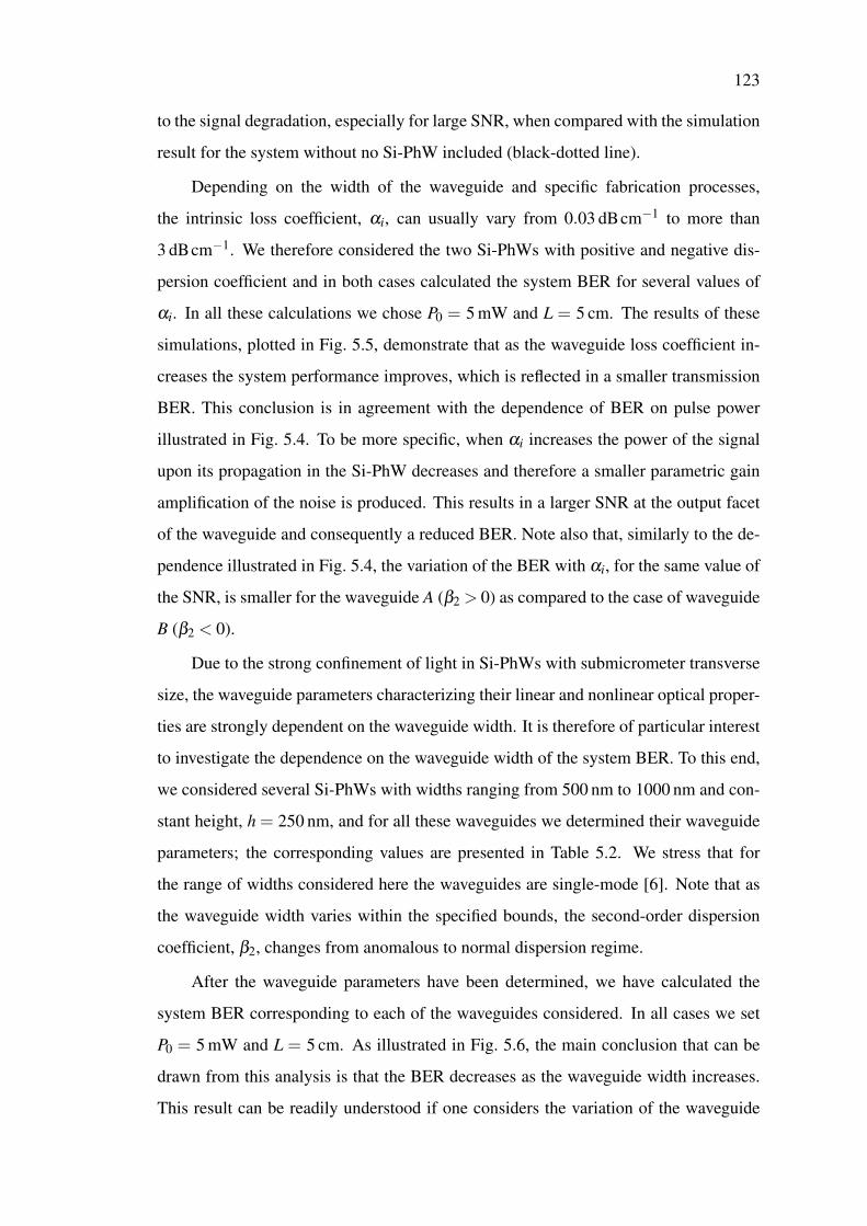
123
to the signal degradation, especially for large SNR, when compared with the simulation
result for the system without no Si-PhW included (black-dotted line).
Depending on the width of the waveguide and specific fabrication processes,
the intrinsic loss coefficient, αi, can usually vary from 0.03 dBcm−1 to more than
3 dBcm−1. We therefore considered the two Si-PhWs with positive and negative dis-
persion coefficient and in both cases calculated the system BER for several values of
αi. In all these calculations we chose P0 = 5 mW and L = 5 cm. The results of these
simulations, plotted in Fig. 5.5, demonstrate that as the waveguide loss coefficient in-
creases the system performance improves, which is reflected in a smaller transmission
BER. This conclusion is in agreement with the dependence of BER on pulse power
illustrated in Fig. 5.4. To be more specific, when αi increases the power of the signal
upon its propagation in the Si-PhW decreases and therefore a smaller parametric gain
amplification of the noise is produced. This results in a larger SNR at the output facet
of the waveguide and consequently a reduced BER. Note also that, similarly to the de-
pendence illustrated in Fig. 5.4, the variation of the BER with αi, for the same value of
the SNR, is smaller for the waveguide A (β2 > 0) as compared to the case of waveguide
B (β2 < 0).
Due to the strong confinement of light in Si-PhWs with submicrometer transverse
size, the waveguide parameters characterizing their linear and nonlinear optical proper-
ties are strongly dependent on the waveguide width. It is therefore of particular interest
to investigate the dependence on the waveguide width of the system BER. To this end,
we considered several Si-PhWs with widths ranging from 500 nm to 1000 nm and con-
stant height, h = 250 nm, and for all these waveguides we determined their waveguide
parameters; the corresponding values are presented in Table 5.2. We stress that for
the range of widths considered here the waveguides are single-mode [6]. Note that as
the waveguide width varies within the specified bounds, the second-order dispersion
coefficient, β2, changes from anomalous to normal dispersion regime.
After the waveguide parameters have been determined, we have calculated the
system BER corresponding to each of the waveguides considered. In all cases we set
P0 = 5 mW and L = 5 cm. As illustrated in Fig. 5.6, the main conclusion that can be
drawn from this analysis is that the BER decreases as the waveguide width increases.
This result can be readily understood if one considers the variation of the waveguide
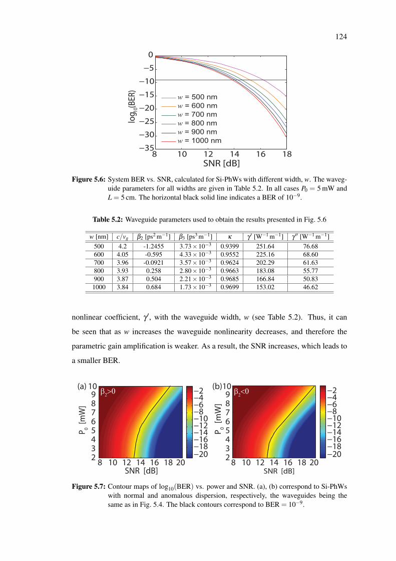
124
8 10 12 14 16 18−35
−30
−25
−20
−15
−10
−5
0
SNR [dB]
log 1
0 (BER)
w = 500 nm
w = 600 nm
w = 700 nm
w = 800 nm
w = 900 nm
w = 1000 nm
Figure 5.6: System BER vs. SNR, calculated for Si-PhWs with different width, w. The waveg-uide parameters for all widths are given in Table 5.2. In all cases P0 = 5 mW andL = 5 cm. The horizontal black solid line indicates a BER of 10−9.
Table 5.2: Waveguide parameters used to obtain the results presented in Fig. 5.6
w [nm] c/vg β2 [ps2 m−1] β3 [ps3 m−1] κ γ ′ [W−1 m−1] γ ′′ [W−1 m−1]500 4.2 -1.2455 3.73×10⁻³ 0.9399 251.64 76.68600 4.05 -0.595 4.33×10⁻³ 0.9552 225.16 68.60700 3.96 -0.0921 3.57×10⁻³ 0.9624 202.29 61.63800 3.93 0.258 2.80×10⁻³ 0.9663 183.08 55.77900 3.87 0.504 2.21×10⁻³ 0.9685 166.84 50.83
1000 3.84 0.684 1.73×10⁻³ 0.9699 153.02 46.62
nonlinear coefficient, γ ′, with the waveguide width, w (see Table 5.2). Thus, it can
be seen that as w increases the waveguide nonlinearity decreases, and therefore the
parametric gain amplification is weaker. As a result, the SNR increases, which leads to
a smaller BER.
SNR [dB]
P0 [
mW
]
8 10 12 14 16 18 2023456789
10
−20−18−16−14−12−10−8−6−4−2β
2>0
SNR [dB]
P0
[mW
]
8 10 12 14 16 18 2023456789
10
−20−18−16−14−12−10−8−6−4−2β
2<0
(a) (b)
Figure 5.7: Contour maps of log10(BER) vs. power and SNR. (a), (b) correspond to Si-PhWswith normal and anomalous dispersion, respectively, the waveguides being thesame as in Fig. 5.4. The black contours correspond to BER = 10−9.
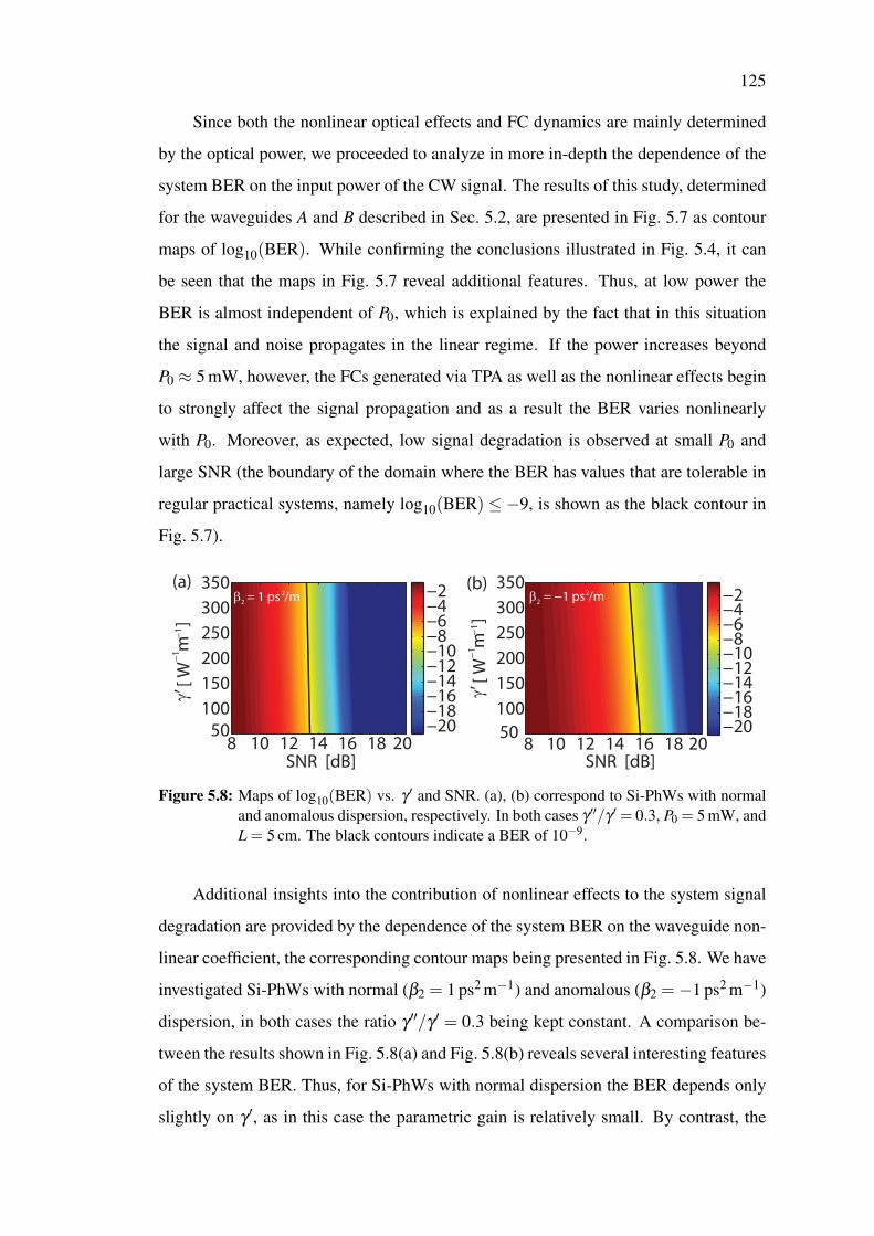
125
Since both the nonlinear optical effects and FC dynamics are mainly determined
by the optical power, we proceeded to analyze in more in-depth the dependence of the
system BER on the input power of the CW signal. The results of this study, determined
for the waveguides A and B described in Sec. 5.2, are presented in Fig. 5.7 as contour
maps of log10(BER). While confirming the conclusions illustrated in Fig. 5.4, it can
be seen that the maps in Fig. 5.7 reveal additional features. Thus, at low power the
BER is almost independent of P0, which is explained by the fact that in this situation
the signal and noise propagates in the linear regime. If the power increases beyond
P0 ≈ 5 mW, however, the FCs generated via TPA as well as the nonlinear effects begin
to strongly affect the signal propagation and as a result the BER varies nonlinearly
with P0. Moreover, as expected, low signal degradation is observed at small P0 and
large SNR (the boundary of the domain where the BER has values that are tolerable in
regular practical systems, namely log10(BER) ≤ −9, is shown as the black contour in
Fig. 5.7).
SNR [dB]
8 10 12 14 16 18 2050
100
150
200
250
300
350
−20−18−16−14−12−10−8−6−4−2β
2 = 1 ps 2/m
(a)
SNR [dB]
8 10 12 14 16 18 2050
100
150
200
250
300
350
−20−18−16−14−12−10−8−6−4−2β
2= −1 ps2/m
(b)
γ′ [
W−
1 m−
1]
γ′ [
W−
1 m−
1]
Figure 5.8: Maps of log10(BER) vs. γ ′ and SNR. (a), (b) correspond to Si-PhWs with normaland anomalous dispersion, respectively. In both cases γ ′′/γ ′ = 0.3, P0 = 5 mW, andL = 5 cm. The black contours indicate a BER of 10−9.
Additional insights into the contribution of nonlinear effects to the system signal
degradation are provided by the dependence of the system BER on the waveguide non-
linear coefficient, the corresponding contour maps being presented in Fig. 5.8. We have
investigated Si-PhWs with normal (β2 = 1 ps2 m−1) and anomalous (β2 = −1 ps2 m−1)
dispersion, in both cases the ratio γ ′′/γ ′ = 0.3 being kept constant. A comparison be-
tween the results shown in Fig. 5.8(a) and Fig. 5.8(b) reveals several interesting features
of the system BER. Thus, for Si-PhWs with normal dispersion the BER depends only
slightly on γ ′, as in this case the parametric gain is relatively small. By contrast, the
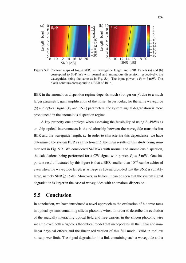
126
SNR [dB]
Le
ng
th [
cm]
8 10 12 14 16 18 2023456789
10
−20−18−16−14−12−10−8−6−4−2(a)
β2>0
SNR [dB]
8 10 12 14 16 18 2023456789
10
−20−18−16−14−12−10−8−6−4−2β
2<0
Le
ng
th [
cm]
(b)
Figure 5.9: Contour maps of log10(BER) vs. waveguide length and SNR. Panels (a) and (b)correspond to Si-PhWs with normal and anomalous dispersion, respectively, thewaveguides being the same as in Fig. 5.4. The input power is P0 = 5 mW. Theblack contours correspond to a BER of 10−9.
BER in the anomalous dispersion regime depends much stronger on γ ′, due to a much
larger parametric gain amplification of the noise. In particular, for the same waveguide
(γ) and optical signal (P0 and SNR) parameters, the system signal degradation is more
pronounced in the anomalous dispersion regime.
A key property one employs when assessing the feasibility of using Si-PhWs as
on-chip optical interconnects is the relationship between the waveguide transmission
BER and the waveguide length, L. In order to characterize this dependence, we have
determined the system BER as a function of L, the main results of this study being sum-
marized in Fig. 5.9. We considered Si-PhWs with normal and anomalous dispersion,
the calculations being performed for a CW signal with power, P0 = 5 mW. One im-
portant result illustrated by this figure is that a BER smaller than 10−9 can be achieved
even when the waveguide length is as large as 10 cm, provided that the SNR is suitably
large, namely SNR & 15 dB. Moreover, as before, it can be seen that the system signal
degradation is larger in the case of waveguides with anomalous dispersion.
5.5 ConclusionIn conclusion, we have introduced a novel approach to the evaluation of bit error rates
in optical systems containing silicon photonic wires. In order to describe the evolution
of the mutually interacting optical field and free-carriers in the silicon photonic wire
we employed both a rigorous theoretical model that incorporates all the linear and non-
linear physical effects and the linearized version of this full model, valid in the low
noise power limit. The signal degradation in a link containing such a waveguide and a
127
direct-detection optical receiver made of an optical filter, an ideal square-law photode-
tector, and an electrical filter was evaluated by using the time domain Karhunen-Loeve
expansion method. This approach was used to study the dependence of the bit error
rate on waveguide and optical signal parameters. In particular, we have determined the
domain in the system parameters space in which the signal degradation remains below
a certain threshold used in practical settings to assess the fidelity of detected signals. It
should be noted that the method introduced here can be easily extended to other silicon
based components of on-chip and chip-to-chip optical networks, including modulators,
amplifiers, optical switches, and frequency converters. Equally important, our formal-
ism can be applied to physical settings in which additional optical effects can become
important. For example, our approach could readily incorporate nonlinear effects such
as four-wave mixing and stimulated Raman scattering, which can become large enough
to affect the bit error rate in properly designed waveguides or for shorter optical pulses.
In the next chapter, the comparative study of the fast-light and SL regimes within
the single-channel silicon photonic crystal systems will be demonstrated, with the sys-
tem using OOK modulated CW signals.
128
Bibliography[1] X. Chen, N. C. Panoiu, and R. M. Osgood, “Theory of Raman-mediated pulsed
amplification in silicon-wire waveguides,” IEEE J. Quantum Electron. 42, 160-
170 (2006).
[2] A. Papoulis, Probability, Random Variables, and Stochastic Processes 3rd ed,
(McGraw-Hill, New York, 1991).
[3] G. Bosco, A. Carena, V. Curri, R. Gaudino, P. Poggiolini, and S. Benedetto, “A
novel analytical approach to the evaluation of the impact of fiber parametric gain
on the bit error rate,” IEEE Trans. Commun. 49, 2154-2163 (2001).
[4] E. Forestieri and M. Secondini, “On the Error Probability Evaluation in Lightwave
Systems With Optical Amplification,” IEEE J. Lightwave Technol. 27, 706-717
(2009).
[5] Q. Lin, O. J. Painter, and G. P. Agrawal, “Nonlinear optical phenomena in silicon
waveguides: Modeling and applications,” Opt. Express 15, 16604-16644 (2007).
[6] S. Lavdas, J. B. Driscoll, R. R. Grote, R. M. Osgood, and N. C. Panoiu, “Pulse
compression in adiabatically tapered silicon photonic wires,” Opt. Express 22,
6296-6312 (2014).
[7] K. Kikuchi, “Enhancement of optical-amplifier noise by nonlinear refractive in-
dex and group-velocity dispersion of optical fibers,” IEEE Photon. Technol. Lett.
5, 221-223 (1993).
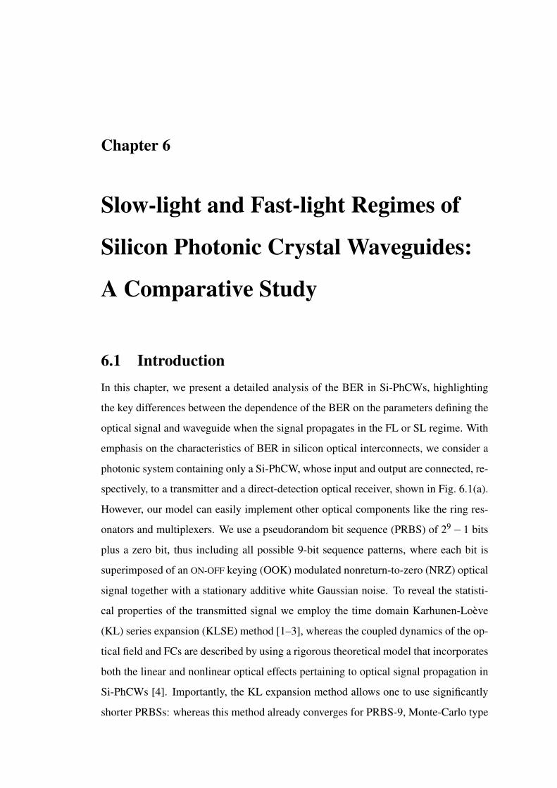
Chapter 6
Slow-light and Fast-light Regimes of
Silicon Photonic Crystal Waveguides:
A Comparative Study
6.1 IntroductionIn this chapter, we present a detailed analysis of the BER in Si-PhCWs, highlighting
the key differences between the dependence of the BER on the parameters defining the
optical signal and waveguide when the signal propagates in the FL or SL regime. With
emphasis on the characteristics of BER in silicon optical interconnects, we consider a
photonic system containing only a Si-PhCW, whose input and output are connected, re-
spectively, to a transmitter and a direct-detection optical receiver, shown in Fig. 6.1(a).
However, our model can easily implement other optical components like the ring res-
onators and multiplexers. We use a pseudorandom bit sequence (PRBS) of 29−1 bits
plus a zero bit, thus including all possible 9-bit sequence patterns, where each bit is
superimposed of an ON-OFF keying (OOK) modulated nonreturn-to-zero (NRZ) optical
signal together with a stationary additive white Gaussian noise. To reveal the statisti-
cal properties of the transmitted signal we employ the time domain Karhunen-Loeve
(KL) series expansion (KLSE) method [1–3], whereas the coupled dynamics of the op-
tical field and FCs are described by using a rigorous theoretical model that incorporates
both the linear and nonlinear optical effects pertaining to optical signal propagation in
Si-PhCWs [4]. Importantly, the KL expansion method allows one to use significantly
shorter PRBSs: whereas this method already converges for PRBS-9, Monte-Carlo type
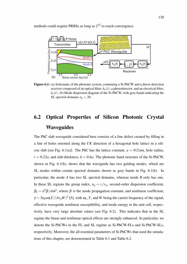
130
methods could require PRBSs as long as 232 to reach convergence.
PhC Waveguide
ho(t)he(t)
Transmitter
0 1 01 1 0 Noiseu(z,t)+a(z,t)
y(t)
Receiver
0.29
0.25
0.21
Fre
qu
en
cy (
ωa
/2π
c)
0.3 0.4 0.5Wave vector (ka/2π)
Mode A
Mode B
(a)
(b)
Figure 6.1: (a) Schematic of the photonic system, containing a Si-PhCW and a direct-detectionreceiver composed of an optical filter, ho(t), a photodetector, and an electrical filter,he(t). (b) Mode dispersion diagram of the Si-PhCW, with grey bands indicating theSL spectral domains ng > 20.
6.2 Optical Properties of Silicon Photonic Crystal
WaveguidesThe PhC slab waveguide considered here consists of a line defect created by filling in
a line of holes oriented along the ΓK direction of a hexagonal hole lattice in a sili-
con slab [see Fig. 6.1(a)]. The PhC has the lattice constant, a = 412nm, hole radius,
r = 0.22a, and slab thickness, h = 0.6a. The photonic band structure of the Si-PhCW,
shown in Fig. 6.1(b), shows that the waveguide has two guiding modes, which are
SL modes within certain spectral domains shown as grey bands in Fig. 6.1(b). In
particular, the mode A has two SL spectral domains, whereas mode B only has one.
In these SL regions the group index, ng = c/vg, second-order dispersion coefficient,
β2 = d2β/dω2, where β is the mode propagation constant, and nonlinear coefficient,
γ = 3ε0aωcΓ/(4vgW )2 [5], with ωc, Γ, and W being the carrier frequency of the signal,
effective waveguide nonlinear susceptibility, and mode energy in the unit cell, respec-
tively, have very large absolute values (see Fig. 6.2). This indicates that in the SL
regime the linear and nonlinear optical effects are strongly enhanced. In particular, we
denote the Si-PhCWs in the FL and SL regime as Si-PhCW-FLs and Si-PhCW-SLs,
respectively. Moreover, the all essential parameters of Si-PhCWs that used the simula-
tions of this chapter, are demonstrated in Table 6.1 and Table 6.2.
131
−1
0
1
x 10−20
β2[s
2/m
]
1.52 1.56 1.6 1.64 1.680
4
8
0
4
8
γ’ [
W-1
m-1
]
γ’’
[W-1
m-1
]
x 103
x 103
λ [μm]
(c)
(b)−80
−40
0
40
80
ng
(a)
Mode B
Mode A
Mode A
Mode A
Mode B
Mode B
Figure 6.2: (a), (b), (c) Wavelength dependence of ng, β2, and γ ′ and γ ′′, respectively, deter-mined for mode A (red lines) and mode B (blue lines). The shaded areas correspondto the SL regime, defined by the relation ng > 20.
6.3 Optical Signal Propagation ApproachThe full mathematical analysis for the signal propagation in the Si-PhCWs is described
by a modified nonlinear Schrodinger equation (Eq. (2.15)), coupled to a rate equation
(Eq. (2.20)) for the FCs. Similarly, several optical parameters will be assigned here.
The intrinsic loss coefficient αin was set to αin = 50dBcm−1, whose value is chosen due
to the roughness of Si-PhCWs. However, the intrinsic loss indeed vary with different
values of group index vg in our model, which is suggested by the first term on the right
side of Eq. (2.15). The FC absorption (FCA) coefficient is αfc = σαN, and the FC-
induced refractive index change is assumed to be δnfc = σnN, where λ = 1550nm, N
is the FC density, σα = 1.45×10⁻²¹(λ/λ )2 (in units of m2). σn = σ0(λ/λ )2 (in units
of m3), with σ0 being a power dependent coefficient [6]. The FC relaxation time tc is
0.5ns in our analysis. Moreover, all dispersive and nonlinear coefficients of Si-PhCWs
are much larger than that of Si-PhWs, which explains the reason why the waveguide
length of Si-PhCWs is far shorter than the Si-PhWs.
The input noisy signal is expressed as Eq. (5.1), which consists of the optical CW
signal with power P(z) and a complex additive Gaussian noise a(z, t). We have used
two methods to determine the optical field at the output of the Si-PhCW. In the first
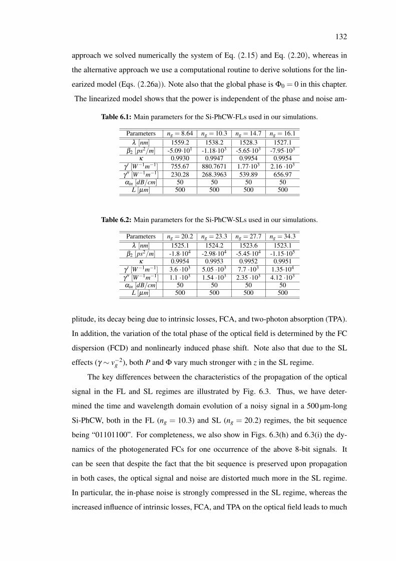
132
approach we solved numerically the system of Eq. (2.15) and Eq. (2.20), whereas in
the alternative approach we use a computational routine to derive solutions for the lin-
earized model (Eqs. (2.26a)). Note also that the global phase is Φ0 = 0 in this chapter.
The linearized model shows that the power is independent of the phase and noise am-
Table 6.1: Main parameters for the Si-PhCW-FLs used in our simulations.
Parameters ng = 8.64 ng = 10.3 ng = 14.7 ng = 16.1λ [nm] 1559.2 1538.2 1528.3 1527.1
β2 [ps2/m] -5.09·101 -1.18·103 -5.65·103 -7.95·103
κ 0.9930 0.9947 0.9954 0.9954γ ′ [W−1m−1] 755.67 880.7671 1.77·103 2.16 ·103
γ ′′ [W−1m−1] 230.28 268.3963 539.89 656.97αin [dB/cm] 50 50 50 50
L [µm] 500 500 500 500
Table 6.2: Main parameters for the Si-PhCW-SLs used in our simulations.
Parameters ng = 20.2 ng = 23.3 ng = 27.7 ng = 34.3λ [nm] 1525.1 1524.2 1523.6 1523.1
β2 [ps2/m] -1.8·104 -2.98·104 -5.45·104 -1.15·105
κ 0.9954 0.9953 0.9952 0.9951γ ′ [W−1m−1] 3.6 ·103 5.05 ·103 7.7 ·103 1.35·104
γ ′′ [W−1m−1] 1.1 ·103 1.54 ·103 2.35 ·103 4.12 ·103
αin [dB/cm] 50 50 50 50L [µm] 500 500 500 500
plitude, its decay being due to intrinsic losses, FCA, and two-photon absorption (TPA).
In addition, the variation of the total phase of the optical field is determined by the FC
dispersion (FCD) and nonlinearly induced phase shift. Note also that due to the SL
effects (γ ∼ v−2g ), both P and Φ vary much stronger with z in the SL regime.
The key differences between the characteristics of the propagation of the optical
signal in the FL and SL regimes are illustrated by Fig. 6.3. Thus, we have deter-
mined the time and wavelength domain evolution of a noisy signal in a 500 µm-long
Si-PhCW, both in the FL (ng = 10.3) and SL (ng = 20.2) regimes, the bit sequence
being “01101100”. For completeness, we also show in Figs. 6.3(h) and 6.3(i) the dy-
namics of the photogenerated FCs for one occurrence of the above 8-bit signals. It
can be seen that despite the fact that the bit sequence is preserved upon propagation
in both cases, the optical signal and noise are distorted much more in the SL regime.
In particular, the in-phase noise is strongly compressed in the SL regime, whereas the
increased influence of intrinsic losses, FCA, and TPA on the optical field leads to much
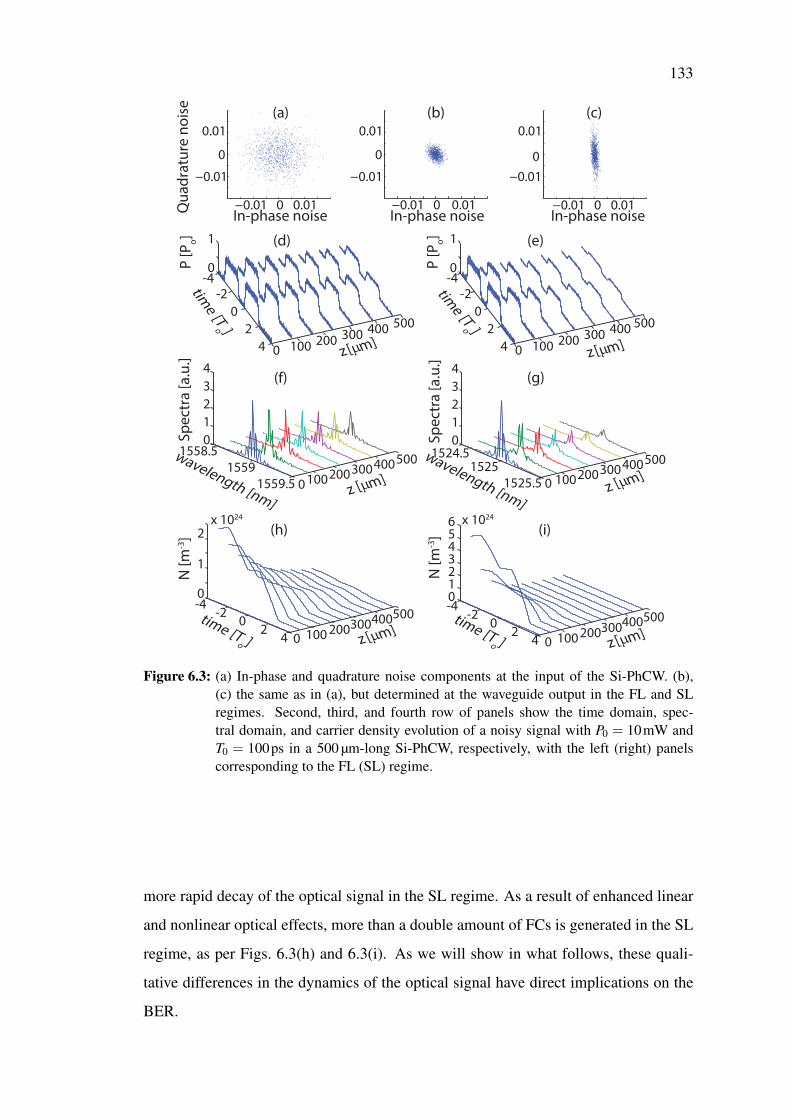
133
−0.01 0 0.01
−0.01
0
0.01
In-phase noise
Qu
ad
ratu
re n
ois
e
−0.01 0 0.01
−0.01
0
0.01
In-phase noise−0.01 0 0.01
−0.01
0
0.01
In-phase noise
(a) (b) (c)
0 100 200 300 400 500
4
2
0
-2-40
1
z [µm]
time [T
o ]
0100200300400500
1559.5
1559
1558.50
1
2
3
4
z [µm]
wavelength [nm]
Sp
ect
ra [
a.u
.]
(d)
(f)
0 100 200 300 400 500
4
2
0
-2-40
1
z [µm]tim
e [To ]
P [
Po]
0 100200300400500
1525.5
15251524.5
0
1
2
3
4
z [µm]
Sp
ect
ra [
a.u
.]
(e)
(g)
P [
Po]
wavelength [nm]
0 100 200300400500
0
1
2
N [
m-3
]
42
0-2
-4time [T
o ]
x 1024
z [µm]4
20
-2-40123456 x 1024
N [
m-3
]
time [To ] 0 100 200300400500
z [µm]
(h) (i)
Figure 6.3: (a) In-phase and quadrature noise components at the input of the Si-PhCW. (b),(c) the same as in (a), but determined at the waveguide output in the FL and SLregimes. Second, third, and fourth row of panels show the time domain, spec-tral domain, and carrier density evolution of a noisy signal with P0 = 10mW andT0 = 100ps in a 500 µm-long Si-PhCW, respectively, with the left (right) panelscorresponding to the FL (SL) regime.
more rapid decay of the optical signal in the SL regime. As a result of enhanced linear
and nonlinear optical effects, more than a double amount of FCs is generated in the SL
regime, as per Figs. 6.3(h) and 6.3(i). As we will show in what follows, these quali-
tative differences in the dynamics of the optical signal have direct implications on the
BER.
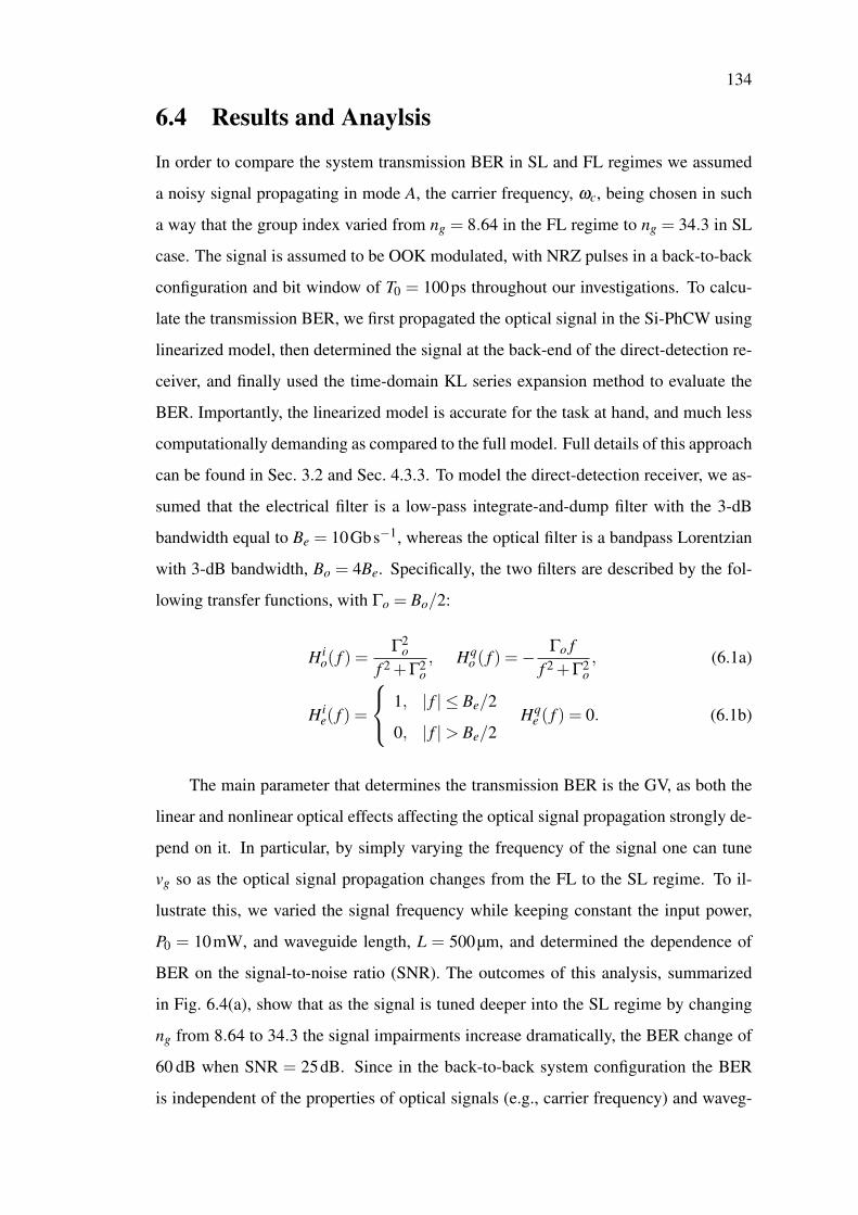
134
6.4 Results and Anaylsis
In order to compare the system transmission BER in SL and FL regimes we assumed
a noisy signal propagating in mode A, the carrier frequency, ωc, being chosen in such
a way that the group index varied from ng = 8.64 in the FL regime to ng = 34.3 in SL
case. The signal is assumed to be OOK modulated, with NRZ pulses in a back-to-back
configuration and bit window of T0 = 100ps throughout our investigations. To calcu-
late the transmission BER, we first propagated the optical signal in the Si-PhCW using
linearized model, then determined the signal at the back-end of the direct-detection re-
ceiver, and finally used the time-domain KL series expansion method to evaluate the
BER. Importantly, the linearized model is accurate for the task at hand, and much less
computationally demanding as compared to the full model. Full details of this approach
can be found in Sec. 3.2 and Sec. 4.3.3. To model the direct-detection receiver, we as-
sumed that the electrical filter is a low-pass integrate-and-dump filter with the 3-dB
bandwidth equal to Be = 10Gbs−1, whereas the optical filter is a bandpass Lorentzian
with 3-dB bandwidth, Bo = 4Be. Specifically, the two filters are described by the fol-
lowing transfer functions, with Γo = Bo/2:
H io( f ) =
Γ2o
f 2 +Γ2o, Hq
o ( f ) =− Γo ff 2 +Γ2
o, (6.1a)
H ie( f ) =
1, | f | ≤ Be/2
0, | f |> Be/2Hq
e ( f ) = 0. (6.1b)
The main parameter that determines the transmission BER is the GV, as both the
linear and nonlinear optical effects affecting the optical signal propagation strongly de-
pend on it. In particular, by simply varying the frequency of the signal one can tune
vg so as the optical signal propagation changes from the FL to the SL regime. To il-
lustrate this, we varied the signal frequency while keeping constant the input power,
P0 = 10mW, and waveguide length, L = 500µm, and determined the dependence of
BER on the signal-to-noise ratio (SNR). The outcomes of this analysis, summarized
in Fig. 6.4(a), show that as the signal is tuned deeper into the SL regime by changing
ng from 8.64 to 34.3 the signal impairments increase dramatically, the BER change of
60 dB when SNR = 25dB. Since in the back-to-back system configuration the BER
is independent of the properties of optical signals (e.g., carrier frequency) and waveg-
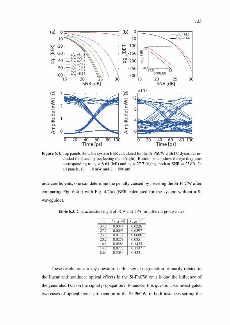
135
(a)
0
1
2
3
Am
pli
tud
e [
mW
]
0 20 40 60 80 100Time [ps]
×10-2
Am
pli
tud
e [
mW
]
(c)
(b)
(d)
0
4
8
12
0 20 40 60 80 100Time [ps]
15 20 25 30SNR [dB]
-60
-50
-40
-30
-20
-10
0
log
10(B
ER
)
15 20 25 30SNR [dB]
-300
-250
-200
-150
-100
-50
0
log
10(B
ER
)
=34.3=27.7=23.3=20.2=16.1=14.7=8.64
c/vgc/vg
c/vg
c/vg
c/vg
c/vg
c/vg
c/vg=34.3c/vg=8.64
24.5 25SNR[dB]
-87
-77
log
10(B
ER
)
Figure 6.4: Top panels show the system BER calculated for the Si-PhCW with FC dynamics in-cluded (left) and by neglecting them (right). Bottom panels show the eye diagramscorresponding to ng = 8.64 (left) and ng = 27.7 (right), both at SNR = 25 dB. Inall panels, P0 = 10 mW and L = 500 µm.
uide coefficients, one can determine the penalty caused by inserting the Si-PhCW after
comparing Fig. 6.4(a) with Fig. 4.2(a) (BER calculated for the system without a Si
waveguide).
Table 6.3: Characteristic length of FCA and TPA for different group-index.
ng LFCA [m] LT PA [m]
34.3 0.0044 0.022627.7 0.0095 0.039723.3 0.0172 0.060620.2 0.0278 0.085116.1 0.0583 0.142514.7 0.0777 0.17378.64 0.3034 0.4231
These results raise a key question: is this signal degradation primarily related to
the linear and nonlinear optical effects in the Si-PhCW or it is due the influence of
the generated FCs on the signal propagation? To answer this question, we investigated
two cases of optical signal propagation in the Si-PhCW, in both instances setting the
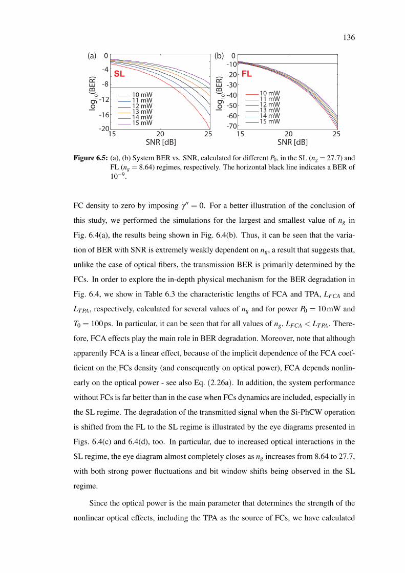
136
(a)
log
10(B
ER
)
15 20 25-20
-16
-12
-8
-4
0
SL
10 mW11 mW12 mW13 mW14 mW15 mW
log
10(B
ER
)
(b)
-70
-60
-50
-40
-30
-20
-10
0
15 20 25
SNR [dB]
FL
10 mW11 mW12 mW13 mW14 mW15 mW
SNR [dB]
Figure 6.5: (a), (b) System BER vs. SNR, calculated for different P0, in the SL (ng = 27.7) andFL (ng = 8.64) regimes, respectively. The horizontal black line indicates a BER of10−9.
FC density to zero by imposing γ ′′ = 0. For a better illustration of the conclusion of
this study, we performed the simulations for the largest and smallest value of ng in
Fig. 6.4(a), the results being shown in Fig. 6.4(b). Thus, it can be seen that the varia-
tion of BER with SNR is extremely weakly dependent on ng, a result that suggests that,
unlike the case of optical fibers, the transmission BER is primarily determined by the
FCs. In order to explore the in-depth physical mechanism for the BER degradation in
Fig. 6.4, we show in Table 6.3 the characteristic lengths of FCA and TPA, LFCA and
LT PA, respectively, calculated for several values of ng and for power P0 = 10mW and
T0 = 100ps. In particular, it can be seen that for all values of ng, LFCA < LT PA. There-
fore, FCA effects play the main role in BER degradation. Moreover, note that although
apparently FCA is a linear effect, because of the implicit dependence of the FCA coef-
ficient on the FCs density (and consequently on optical power), FCA depends nonlin-
early on the optical power - see also Eq. (2.26a). In addition, the system performance
without FCs is far better than in the case when FCs dynamics are included, especially in
the SL regime. The degradation of the transmitted signal when the Si-PhCW operation
is shifted from the FL to the SL regime is illustrated by the eye diagrams presented in
Figs. 6.4(c) and 6.4(d), too. In particular, due to increased optical interactions in the
SL regime, the eye diagram almost completely closes as ng increases from 8.64 to 27.7,
with both strong power fluctuations and bit window shifts being observed in the SL
regime.
Since the optical power is the main parameter that determines the strength of the
nonlinear optical effects, including the TPA as the source of FCs, we have calculated
137
the dependence of the BER on the SNR, for different values of P0. The results of
these calculations, presented in Fig. 6.5, show that, irrespective of P0, a much better
system performance is achieved in the FL regime (ng = 8.64) than in the SL regime
(ng = 27.7). This is primarily due to the fact that the Si-PhCW operating in the SL
regime has a much larger nonlinear coefficient, which leads both to a larger parametric
gain amplification of the noise and to increased amount of FCs. To be more specific,
γ is proportional to v−2g and therefore in the SL regime the parametric gain responsible
for noise amplification (∼γ ′) and TPA (∼γ ′′) are enhanced. Consequently, the signal
degradation increases, leading to larger BER. In addition, TPA increases with P0, too,
which explains why the BER increases with P0. One last idea illustrated by Fig. 6.5 is
that in the SL regime the BER varies much stronger with P0 as compared to this power
variation in the FL regime.
6.5 ConclusionIn conclusion, we studied the transmission BER in silicon photonic crystal waveguides
and contrasted the results obtained in two relevant cases, namely when the optical signal
propagates in the fast- and slow-light regimes. Our analysis revealed that although
slow-light effects provide the key advantage of increased nonlinearity, they also lead
to detrimental consequences, including a significant degradation of the transmission
BER. Theoretical and computational investigations showed that the signal impairments
are primarily due to the generation of free carriers.
When compared with the OOK modulation, the PSK modulated signals have ad-
vantage in increasing the spectral efficiency and enlarging the system capacity. There-
fore, the study of single-channel Si photonic systems that utilizing higher-order PSK
modulation will be described in the next chapter.
138
Bibliography[1] A. Papoulis, Probability, Random Variables, and Stochastic Processes 3rd ed,
(McGraw-Hill, New York, 1991).
[2] G. Bosco, A. Carena, V. Curri, R. Gaudino, P. Poggiolini, and S. Benedetto, “A
novel analytical approach to the evaluation of the impact of fiber parametric gain
on the bit error rate,” IEEE Trans. Commun. 49, 2154-2163 (2001).
[3] J. You, and N. C. Panoiu, “Calculation of Bit Error Rates in Optical Systems with
Silicon Photonic Wires,” IEEE J. Quantum Electron. 51, 8400108 (2015).
[4] N. C. Panoiu, J. F. McMillan, and C. W. Wong, “Theoretical Analysis of Pulse Dy-
namics in Silicon Photonic Crystal Wire Waveguides,” IEEE J. Sel. Top. Quantum
Electron. 16, 257-266 (2010).
[5] S. Lavdas and N. C. Panoiu, “Theory of Pulsed Four-Wave-Mixing in One-
dimensional Silicon Photonic Crystal Slab Waveguides,” Phys. Rev. B 93, 115435
(2016).
[6] Q. Lin, O. J. Painter, and G. P. Agrawal,“Nonlinear optical phenomena in silicon
waveguides: Modeling and applications,” Opt. Express 15, 16604-16644 (2007).
Chapter 7
Exploiting Higher-order PSK
Modulation and Direct-detection in
Single-channel Silicon Photonic
Systems
7.1 IntroductionIn this chapter, we study theoretically the performance of photonic systems containing
single-channel Si-PhWs or Si-PhCWs and utilizing PSK, OOK, and ASK-PSK modu-
lated signals. The system investigated in this work consists of a single-mode Si-PhW
or Si-PhCW, the latter being operated either in the fast-light (FL) or slow-light (SL)
regime, linked to a direct-detection receiver containing an intensity-detect branch and
phase-detect branch (see Fig. 7.1). The system dynamics was described by a modi-
fied nonlinear Schrodinger equation governing the propagation of the optical field cou-
pled to a standard rate equation describing the evolution of free-carriers (FCs) [1–5].
Moreover, the statistical properties of the transmitted signal were analyzed using the
frequency-domain Karhunen-Loeve (KL) method [6, 7]. This analysis was performed
for different values of key system parameters and for several modulation formats.
The chapter is organized as follows. In Sec. 7.2, we introduce the models that
govern the propagation of the noisy signal in the Si waveguides. Then, in Sec. 7.3, we
describe the advanced modulation formats and the details of direct-detection receivers
considered in this work. This is followed by the description of the bit-error rate (BER)
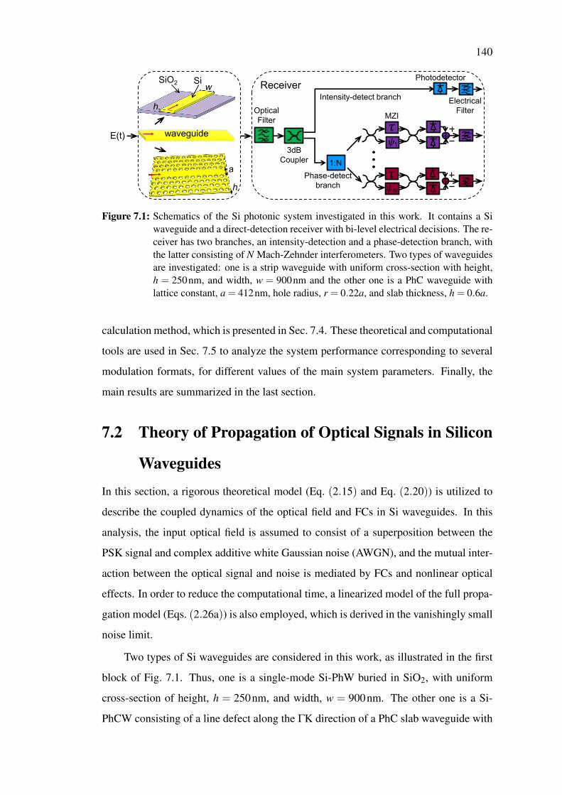
140
1:N
1
w
waveguide
Optical Filter
3dBCoupler
…
Electrical Filter
Photodetector
MZI
ReceiverIntensity-detect branch
Phase-detect branch
E(t)
Figure 7.1: Schematics of the Si photonic system investigated in this work. It contains a Siwaveguide and a direct-detection receiver with bi-level electrical decisions. The re-ceiver has two branches, an intensity-detection and a phase-detection branch, withthe latter consisting of N Mach-Zehnder interferometers. Two types of waveguidesare investigated: one is a strip waveguide with uniform cross-section with height,h = 250nm, and width, w = 900nm and the other one is a PhC waveguide withlattice constant, a = 412nm, hole radius, r = 0.22a, and slab thickness, h = 0.6a.
calculation method, which is presented in Sec. 7.4. These theoretical and computational
tools are used in Sec. 7.5 to analyze the system performance corresponding to several
modulation formats, for different values of the main system parameters. Finally, the
main results are summarized in the last section.
7.2 Theory of Propagation of Optical Signals in Silicon
WaveguidesIn this section, a rigorous theoretical model (Eq. (2.15) and Eq. (2.20)) is utilized to
describe the coupled dynamics of the optical field and FCs in Si waveguides. In this
analysis, the input optical field is assumed to consist of a superposition between the
PSK signal and complex additive white Gaussian noise (AWGN), and the mutual inter-
action between the optical signal and noise is mediated by FCs and nonlinear optical
effects. In order to reduce the computational time, a linearized model of the full propa-
gation model (Eqs. (2.26a)) is also employed, which is derived in the vanishingly small
noise limit.
Two types of Si waveguides are considered in this work, as illustrated in the first
block of Fig. 7.1. Thus, one is a single-mode Si-PhW buried in SiO2, with uniform
cross-section of height, h = 250nm, and width, w = 900nm. The other one is a Si-
PhCW consisting of a line defect along the ΓK direction of a PhC slab waveguide with
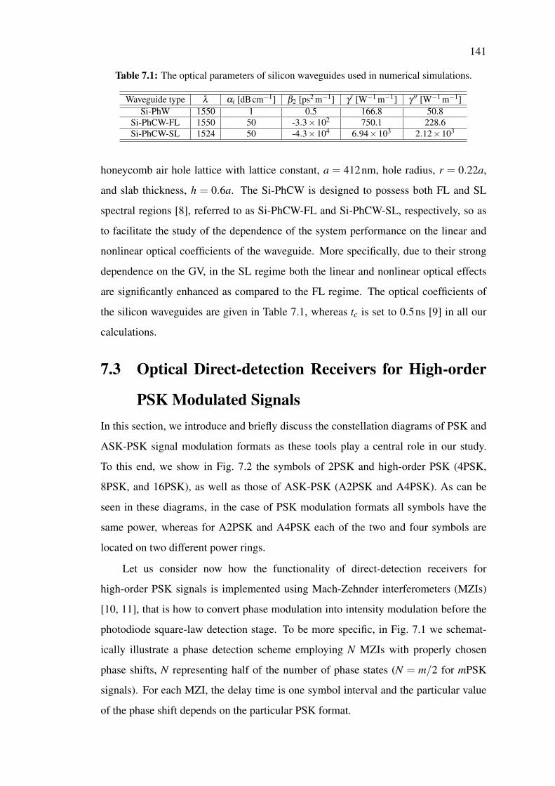
141
Table 7.1: The optical parameters of silicon waveguides used in numerical simulations.
Waveguide type λ αi [dBcm−1] β2 [ps2 m−1] γ ′ [W−1 m−1] γ ′′ [W−1 m−1]Si-PhW 1550 1 0.5 166.8 50.8
Si-PhCW-FL 1550 50 -3.3×10² 750.1 228.6Si-PhCW-SL 1524 50 -4.3×10⁴ 6.94×10³ 2.12×10³
honeycomb air hole lattice with lattice constant, a = 412nm, hole radius, r = 0.22a,
and slab thickness, h = 0.6a. The Si-PhCW is designed to possess both FL and SL
spectral regions [8], referred to as Si-PhCW-FL and Si-PhCW-SL, respectively, so as
to facilitate the study of the dependence of the system performance on the linear and
nonlinear optical coefficients of the waveguide. More specifically, due to their strong
dependence on the GV, in the SL regime both the linear and nonlinear optical effects
are significantly enhanced as compared to the FL regime. The optical coefficients of
the silicon waveguides are given in Table 7.1, whereas tc is set to 0.5ns [9] in all our
calculations.
7.3 Optical Direct-detection Receivers for High-order
PSK Modulated SignalsIn this section, we introduce and briefly discuss the constellation diagrams of PSK and
ASK-PSK signal modulation formats as these tools play a central role in our study.
To this end, we show in Fig. 7.2 the symbols of 2PSK and high-order PSK (4PSK,
8PSK, and 16PSK), as well as those of ASK-PSK (A2PSK and A4PSK). As can be
seen in these diagrams, in the case of PSK modulation formats all symbols have the
same power, whereas for A2PSK and A4PSK each of the two and four symbols are
located on two different power rings.
Let us consider now how the functionality of direct-detection receivers for
high-order PSK signals is implemented using Mach-Zehnder interferometers (MZIs)
[10, 11], that is how to convert phase modulation into intensity modulation before the
photodiode square-law detection stage. To be more specific, in Fig. 7.1 we schemat-
ically illustrate a phase detection scheme employing N MZIs with properly chosen
phase shifts, N representing half of the number of phase states (N = m/2 for mPSK
signals). For each MZI, the delay time is one symbol interval and the particular value
of the phase shift depends on the particular PSK format.
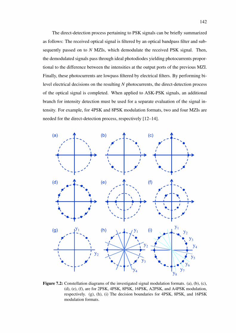
142
The direct-detection process pertaining to PSK signals can be briefly summarized
as follows: The received optical signal is filtered by an optical bandpass filter and sub-
sequently passed on to N MZIs, which demodulate the received PSK signal. Then,
the demodulated signals pass through ideal photodiodes yielding photocurrents propor-
tional to the difference between the intensities at the output ports of the previous MZI.
Finally, these photocurrents are lowpass filtered by electrical filters. By performing bi-
level electrical decisions on the resulting N photocurrents, the direct-detection process
of the optical signal is completed. When applied to ASK-PSK signals, an additional
branch for intensity detection must be used for a separate evaluation of the signal in-
tensity. For example, for 4PSK and 8PSK modulation formats, two and four MZIs are
needed for the direct-detection process, respectively [12–14].
y2
y1 y1
y2
y3
y4
y1
y4
y2y3
y5
y6y7y8
(a) (b) (c)
(d) (e) (f)
(g) (h) (i)
Figure 7.2: Constellation diagrams of the investigated signal modulation formats. (a), (b), (c),(d), (e), (f), are for 2PSK, 4PSK, 8PSK, 16PSK, A2PSK, and A4PSK modulation,respectively. (g), (h), (i) The decision boundaries for 4PSK, 8PSK, and 16PSKmodulation formats.
143
7.4 Methods for Analysis of Direct-detection of PSK
and ASK-PSK SignalsIn this section we present a general formalism for the characterization of direct-
detection of PSK and ASK-PSK signals with particular emphasis on BER calculations.
As an illustration of the general formalism, we show how it applies to the 8PSK mod-
ulation format.
7.4.1 General Case
Our general approach to BER calculations is based on the frequency-domain KL series
expansion of the transmitted signal. Importantly, the KL expansion method allows
one to use much shorter pseudorandom bit sequences (PRBSs): whereas it already
converges for PRBS-9, Monte-Carlo type methods could require PRBSs as long as 232
to reach convergence [11].
The basic idea of KL expansion is to obtain the decision variable as a sum of un-
correlated and independent random variables via a set of orthonormal functions. Thus,
starting from the frequency-domain signal at the output of the waveguide, X( f ), the de-
cision variable for the nth port, n= 1, . . . ,N, is expressed as a double Fourier transform:
yn(t) =∫
∞
−∞
∫∞
−∞
X∗( f1)Kn( f1, f2)X( f2)e2πi( f2− f1)td f1d f2, (7.1)
where the kernel Kn( f1, f2) is
Kn( f1, f2) = H∗o ( f2)Ho( f1)He( f1− f2)[H∗n,U( f2)Hn,U( f1)−H∗n,L( f2)Hn,L( f1)]. (7.2)
Here, Ho( f ), He( f ), Hn,U , and Hn,L are the transfer functions of the bandpass optical
filter, lowpass electrical filter, and the upper and lower branch of the nth MZI with the
corresponding couplers included, respectively [12]. The specific forms of Hn,U and
Hn,L depend on the type of the PSK signal. Thus, for mPSK, neglecting the phase error
in MZIs, these functions are:
Hn,U( f ) =12
Cr
(e−2πi f Ts + eiφn
), (7.3a)
Hn,L( f ) =12
Cr
(e−2πi f Ts− eiφn
), (7.3b)
144
where Ts is the symbol duration, φn is the phase shift of the nth MZI, and Cr represents
the coupler coefficients for mPSK and are given by Cr = (√
2/2)r, r = log2 m−1.
The BER calculation for each MZI port is performed by using discrete Fourier
transform. Thus, the frequency interval is discretized to a discrete-frequency vector
with equally spaced values separated by ∆ f . Then, the decision variable in Eq. (7.1)
can be written as a double sum,
y(t) =2M+1
∑α=1
2M+1
∑β=1
x∗αKαβ xβ , (7.4)
where for convenience the port index n has been dropped and
xα = X( fα)e2πi fα t√
∆ f , (7.5a)
Kαβ = K( fα , fβ )∆ f . (7.5b)
Here, M is an integer chosen such that the entire relevant frequency interval is covered
and fα = (α−1−M)∆ f , α = 1, . . . ,2M+1.
For later convenience, we now recast Eq. (7.4) into a real-valued equation. For
this, the signal is converted to a real column vector by concatenating the real and imag-
inary parts of the vector, xα, namely x = [x′ x′′]T , and the kernel K is similarly
converted to a (4M+2)× (4M+2) real matrix, K = [K′ −K′′; K′′ K′]. As a result of
these manipulations, the decision variable y(t) can be expressed as:
y(t) = xT Kx. (7.6)
The covariance matrix associated to statistical variable x, R=ExxTwhere E·
denotes the statistical expectation operator, can be factorized in Cholesky decomposi-
tion as R = ΣΣT , where Σ is a lower-triangular matrix. An orthogonal matrix, Λ, is then
constructed so as to diagonalize the real symmetric matrix ΣT KΣ, namely:
Λ
TΣ
T KΣΛ
α,β= ηαδα,β , (7.7)
where ηα ,α = 1, ...,4M + 2, are real-valued eigenvalues. If we introduce the new
multivariate random variable w = ΛT Σ−1x ≡ ΛT Σ−1s+ΛT Σ−1n, where s and n are
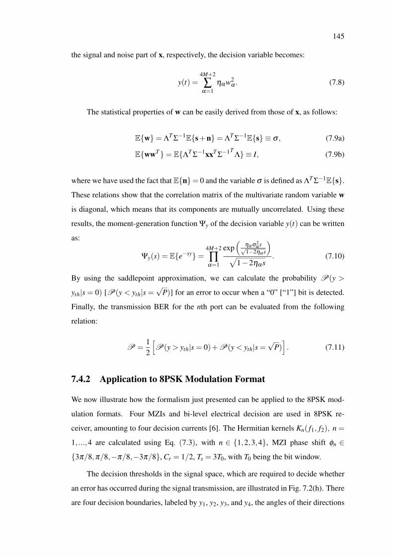
145
the signal and noise part of x, respectively, the decision variable becomes:
y(t) =4M+2
∑α=1
ηαw2α . (7.8)
The statistical properties of w can be easily derived from those of x, as follows:
Ew= ΛT
Σ−1Es+n= Λ
TΣ−1Es ≡ σ , (7.9a)
EwwT= EΛTΣ−1xxT
Σ−1T
Λ ≡ I, (7.9b)
where we have used the fact that En= 0 and the variable σ is defined as ΛT Σ−1Es.
These relations show that the correlation matrix of the multivariate random variable w
is diagonal, which means that its components are mutually uncorrelated. Using these
results, the moment-generation function Ψy of the decision variable y(t) can be written
as:
Ψy(s) = Ee−sy=4M+2
∏α=1
exp(
ηα σ2α s√
1−2ηα s
)√
1−2ηαs. (7.10)
By using the saddlepoint approximation, we can calculate the probability P(y >
yth|s = 0) [P(y < yth|s =√
P)] for an error to occur when a “0” [“1”] bit is detected.
Finally, the transmission BER for the nth port can be evaluated from the following
relation:
P =12
[P(y > yth|s = 0)+P(y < yth|s =
√P)]. (7.11)
7.4.2 Application to 8PSK Modulation Format
We now illustrate how the formalism just presented can be applied to the 8PSK mod-
ulation formats. Four MZIs and bi-level electrical decision are used in 8PSK re-
ceiver, amounting to four decision currents [6]. The Hermitian kernels Kn( f1, f2), n =
1, ...,4 are calculated using Eq. (7.3), with n ∈ 1,2,3,4, MZI phase shift φn ∈
3π/8,π/8,−π/8,−3π/8, Cr = 1/2, Ts = 3T0, with T0 being the bit window.
The decision thresholds in the signal space, which are required to decide whether
an error has occurred during the signal transmission, are illustrated in Fig. 7.2(h). There
are four decision boundaries, labeled by y1, y2, y3, and y4, the angles of their directions
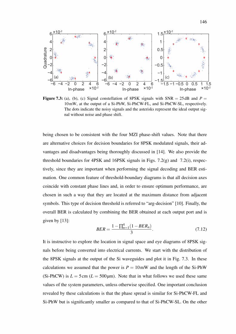
146
−6 −4 −2 0 2 4 6−6
−4
−20
2
4
6
In-phase
Qua
drat
ure
−1.5 −1 −0.5 0 0.5 1 1.5−1.5
−1
−0.5
0
0.5
1
1.5
In-phase
(a) (c)(b)
×10-2
×10-2−6
−4
−20
2
4
6 ×10⁻²
−6 −4 −2 0 2 4 6In-phase ×10-2
×10-2
×10-2
Figure 7.3: (a), (b), (c) Signal constellation of 8PSK signals with SNR = 25dB and P =10mW, at the output of a Si-PhW, Si-PhCW-FL, and Si-PhCW-SL, respectively.The dots indicate the noisy signals and the asterisks represent the ideal output sig-nal without noise and phase shift.
being chosen to be consistent with the four MZI phase-shift values. Note that there
are alternative choices for decision boundaries for 8PSK modulated signals, their ad-
vantages and disadvantages being thoroughly discussed in [14]. We also provide the
threshold boundaries for 4PSK and 16PSK signals in Figs. 7.2(g) and 7.2(i), respec-
tively, since they are important when performing the signal decoding and BER esti-
mation. One common feature of threshold-boundary diagrams is that all decision axes
coincide with constant phase lines and, in order to ensure optimum performance, are
chosen in such a way that they are located at the maximum distance from adjacent
symbols. This type of decision threshold is referred to “arg-decision” [10]. Finally, the
overall BER is calculated by combining the BER obtained at each output port and is
given by [13]:
BER =1−∏
4n=1(1−BERn)
3. (7.12)
It is instructive to explore the location in signal space and eye diagrams of 8PSK sig-
nals before being converted into electrical currents. We start with the distribution of
the 8PSK signals at the output of the Si waveguides and plot it in Fig. 7.3. In these
calculations we assumed that the power is P = 10mW and the length of the Si-PhW
(Si-PhCW) is L = 5cm (L = 500µm). Note that in what follows we used these same
values of the system parameters, unless otherwise specified. One important conclusion
revealed by these calculations is that the phase spread is similar for Si-PhCW-FL and
Si-PhW but is significantly smaller as compared to that of Si-PhCW-SL. On the other
147
hand, the signal amplitude spread in the three cases has similar values. One possible
explanation of this finding is that for Si γ ′′ is about an order of magnitude smaller than
γ ′, meaning that TPA has a weaker effect on the power, as compared to the extent to
which SPM affects the phase. We see that even though the length of Si-PhCW is 100×
shorter than that of the Si-PhW, the Si-PhCW operating in the FL regime leads to much
less degraded signals.
-0.06-0.04-0.02
00.020.040.06
Ampl
itude
-0.06-0.04-0.02
00.020.040.06
Ampl
itude
time [s] ×10-30 1 2 3
-0.06-0.04-0.02
00.020.040.06
time [s] ×10-30 1
-0.06-0.04-0.02
00.020.040.06
2 3
-0.02-0.01
0
0.01
0.02
-0.02-0.01
0
0.01
0.02
time [s] ×10-30 1 2 3
(a) (b) (c)
(d) (e) (f)
Figure 7.4: Top and bottom panels show the eye diagrams of real and imaginary part of received8PSK signals after fifth-order Butterworth optical filter, respectively. From left toright, the panels correspond to the Si-PhW, Si-PhCW-FL, and Si-PhCW-SL. Theinput power P = 10mW, SNR = 25dB, and lengths of Si-PhW and Si-PhCW are5 cm and 500 µm, respectively.
The eye diagrams of the real and imaginary parts of 8PSK signals, after pass-
ing through fifth-order Butterworth optical filter, are shown in Fig. 7.4. The top and
bottom panels represent the real and imaginary part of signals, respectively. These eye
diagrams show that the amplitude decay is comparable in the Si-PhW and Si-PhCW-FL
systems, but is much larger in the Si-PhCW-SL system, a fact explained by increased
linear and nonlinear losses in the SL regime. Moreover, the eye opening is the small-
est in the Si-PhCW-SL system when the eye diagrams are normalized so that a fair
comparison can be made. This conclusion agrees with the results presented in Fig. 7.3.
7.5 Results and DiscussionWe begin this section by describing the set-up of the numerical simulations. Thus, we
use a PRBS of 29− 1 bits plus a zero bit, hence including all possible 9-bit sequence
148
patterns. The bit window is T0 = 100ps and all MZIs in the direct-detection receivers
have a time delay of Ts = 3T0 and modulation-type related phase shifts. Note that the FC
relaxation time (0.5 ns) is much shorter than the total time of the bit sequence (51.2 ns),
which means that steady state is reached in our calculations. In addition, we choose
low-pass integrate-and-dump electrical filters with the 3-dB bandwidth, Be = 10Gbs−1,
and bandpass Lorentzian optical filters with the 3-dB bandwidth, Bo = 4Be [15]. In
order to illustrate the capabilities of our model, other types of filter configurations are
considered, too.
Before presenting the main results of our analysis of the system performance,
we discuss the physical conditions in which our theoretical model is valid as well as
the main physical effects that influence the BER. Thus, if we assume that the sig-
nal power is P = 5mW, the corresponding FC loss coefficient of the Si waveguides,
αfc, is 1.4×10⁻³ dBcm−1, 1.38×10⁻² dBcm−1, and 1.24×10⁻¹ dBcm−1 for the Si-
PhW, Si-PhCW-FL, and Si-PhCW-SL, respectively, all these values being very small
compared to the intrinsic loss coefficient of the Si-PhW (1 dBcm−1) and Si-PhCW
(50 dBcm−1). The same conclusion holds for δnfc, the corresponding values being
−7.91×10⁻⁷ ,−7.73×10⁻⁶ , and−6.93×10⁻⁵ , that is well within the bounds where
FC response is linear. We now turn our attention to the relative strength of dispersive
and nonlinear effects. Using the values in Table 7.1, we find that for P = 10mW and
T0 = 100ps the dispersion length is LD = 2×10⁴ m, LD = 30m, and LD = 0.24m for
the Si-PhW, Si-PhCW-FL, and Si-PhCW-SL, respectively, whereas the corresponding
nonlinear lengths are LNL = 1.97m, LNL = 0.13m, and LNL = 0.014m. This shows
that nonlinearity plays a much more important role than the waveguide dispersion in
defining the optical signal dynamics.
The BER for all modulation formats was simulated for different values of the
signal-to-noise ratio (SNR), for the Si-PhW, Si-PhCW-FL, and Si-PhCW-SL systems
depicted in Fig. 7.1, the results being summarized in Fig. 7.5. A first conclusion of
these numerical investigations is that the system BER increases as the order of PSK
signal increases. In particular, ranked from the highest to lowest BER, the modulation
formats are 16PSK, 8PSK, A4PSK, A2PSK, 4PSK, and 2PSK. Note that in the case
of A4PSK and A2PSK signals, the power in the outer circle was chosen to be twice
as large as that in the inner one and since we set the average power to be the same in
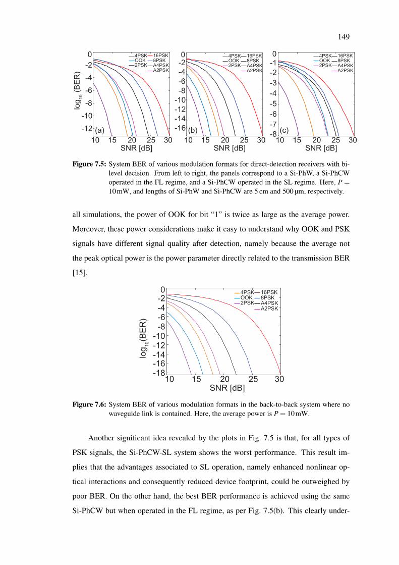
149
log 10
(BER
)
10 15 20 25 30SNR [dB]
-12-10-8-6-4-20 16PSK
8PSKA4PSKA2PSK
4PSKOOK2PSK
-16-14-12-10-8-6-4-20
10 15 20 25 30SNR [dB]
16PSK8PSKA4PSKA2PSK
4PSKOOK2PSK
-8-7-6-5-4-3-2-10 16PSK
8PSKA4PSKA2PSK
4PSKOOK2PSK
10 15 20 25 30SNR [dB]
(a) (b) (c)
Figure 7.5: System BER of various modulation formats for direct-detection receivers with bi-level decision. From left to right, the panels correspond to a Si-PhW, a Si-PhCWoperated in the FL regime, and a Si-PhCW operated in the SL regime. Here, P =10mW, and lengths of Si-PhW and Si-PhCW are 5 cm and 500 µm, respectively.
all simulations, the power of OOK for bit “1” is twice as large as the average power.
Moreover, these power considerations make it easy to understand why OOK and PSK
signals have different signal quality after detection, namely because the average not
the peak optical power is the power parameter directly related to the transmission BER
[15].
10 15 20 25 30SNR [dB]
-18-16-14-12-10
-8-6-4-20
log 10
(BER
)
16PSK8PSKA4PSKA2PSK
4PSKOOK2PSK
Figure 7.6: System BER of various modulation formats in the back-to-back system where nowaveguide link is contained. Here, the average power is P = 10mW.
Another significant idea revealed by the plots in Fig. 7.5 is that, for all types of
PSK signals, the Si-PhCW-SL system shows the worst performance. This result im-
plies that the advantages associated to SL operation, namely enhanced nonlinear op-
tical interactions and consequently reduced device footprint, could be outweighed by
poor BER. On the other hand, the best BER performance is achieved using the same
Si-PhCW but when operated in the FL regime, as per Fig. 7.5(b). This clearly under-
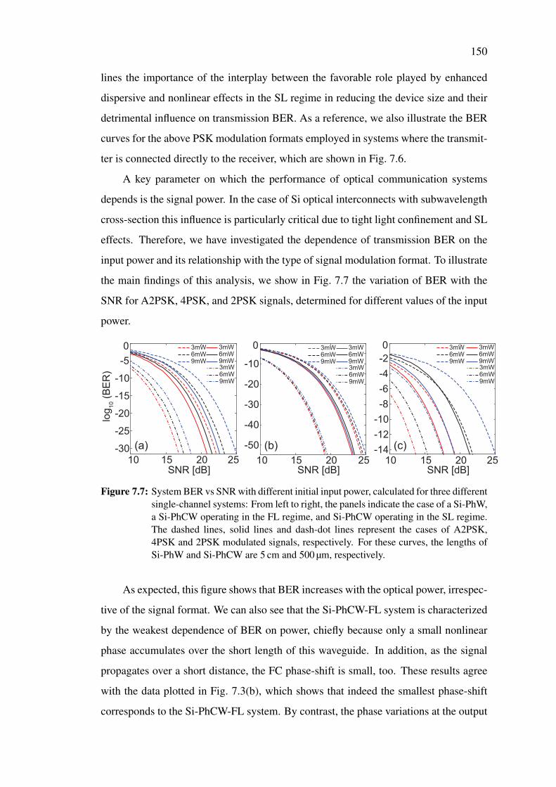
150
lines the importance of the interplay between the favorable role played by enhanced
dispersive and nonlinear effects in the SL regime in reducing the device size and their
detrimental influence on transmission BER. As a reference, we also illustrate the BER
curves for the above PSK modulation formats employed in systems where the transmit-
ter is connected directly to the receiver, which are shown in Fig. 7.6.
A key parameter on which the performance of optical communication systems
depends is the signal power. In the case of Si optical interconnects with subwavelength
cross-section this influence is particularly critical due to tight light confinement and SL
effects. Therefore, we have investigated the dependence of transmission BER on the
input power and its relationship with the type of signal modulation format. To illustrate
the main findings of this analysis, we show in Fig. 7.7 the variation of BER with the
SNR for A2PSK, 4PSK, and 2PSK signals, determined for different values of the input
power.
10 15 20 25SNR [dB]
-30
-25
-20
-15
-10
-50
log 10
(BER
)
3mW6mW9mW
3mW6mW9mW3mW6mW9mW
(a)10 15 20 25
SNR [dB]
-50
-40
-30
-20
-10
0 3mW6mW9mW
3mW6mW9mW3mW6mW9mW
(b)10 15 20 25
SNR [dB]
-14-12-10-8-6-4-20
(c)
3mW6mW9mW
3mW6mW9mW3mW6mW9mW
Figure 7.7: System BER vs SNR with different initial input power, calculated for three differentsingle-channel systems: From left to right, the panels indicate the case of a Si-PhW,a Si-PhCW operating in the FL regime, and Si-PhCW operating in the SL regime.The dashed lines, solid lines and dash-dot lines represent the cases of A2PSK,4PSK and 2PSK modulated signals, respectively. For these curves, the lengths ofSi-PhW and Si-PhCW are 5 cm and 500 µm, respectively.
As expected, this figure shows that BER increases with the optical power, irrespec-
tive of the signal format. We can also see that the Si-PhCW-FL system is characterized
by the weakest dependence of BER on power, chiefly because only a small nonlinear
phase accumulates over the short length of this waveguide. In addition, as the signal
propagates over a short distance, the FC phase-shift is small, too. These results agree
with the data plotted in Fig. 7.3(b), which shows that indeed the smallest phase-shift
corresponds to the Si-PhCW-FL system. By contrast, the phase variations at the output
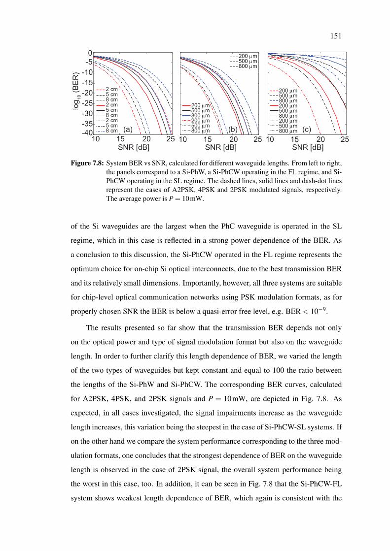
151
10 15 20 25SNR [dB]
-40-35-30-25-20-15-10-50
log 10
(BER
)
2 cm5 cm8 cm2 cm5 cm8 cm2 cm5 cm8 cm (a)
200 µm 500 µm 800 µm 200 µm500 µm 800 µm
200 µm 500 µm800 µm
10 15 20 25SNR [dB]
(b)
200 µm 500 µm 800 µm 200 µm 500 µm 800 µm 200 µm 500 µm 800 µm
10 15 20 25SNR [dB]
(c)
Figure 7.8: System BER vs SNR, calculated for different waveguide lengths. From left to right,the panels correspond to a Si-PhW, a Si-PhCW operating in the FL regime, and Si-PhCW operating in the SL regime. The dashed lines, solid lines and dash-dot linesrepresent the cases of A2PSK, 4PSK and 2PSK modulated signals, respectively.The average power is P = 10mW.
of the Si waveguides are the largest when the PhC waveguide is operated in the SL
regime, which in this case is reflected in a strong power dependence of the BER. As
a conclusion to this discussion, the Si-PhCW operated in the FL regime represents the
optimum choice for on-chip Si optical interconnects, due to the best transmission BER
and its relatively small dimensions. Importantly, however, all three systems are suitable
for chip-level optical communication networks using PSK modulation formats, as for
properly chosen SNR the BER is below a quasi-error free level, e.g. BER < 10−9.
The results presented so far show that the transmission BER depends not only
on the optical power and type of signal modulation format but also on the waveguide
length. In order to further clarify this length dependence of BER, we varied the length
of the two types of waveguides but kept constant and equal to 100 the ratio between
the lengths of the Si-PhW and Si-PhCW. The corresponding BER curves, calculated
for A2PSK, 4PSK, and 2PSK signals and P = 10mW, are depicted in Fig. 7.8. As
expected, in all cases investigated, the signal impairments increase as the waveguide
length increases, this variation being the steepest in the case of Si-PhCW-SL systems. If
on the other hand we compare the system performance corresponding to the three mod-
ulation formats, one concludes that the strongest dependence of BER on the waveguide
length is observed in the case of 2PSK signal, the overall system performance being
the worst in this case, too. In addition, it can be seen in Fig. 7.8 that the Si-PhCW-FL
system shows weakest length dependence of BER, which again is consistent with the
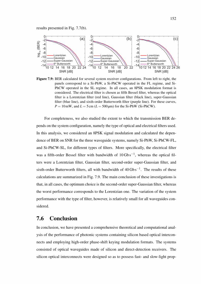
152
results presented in Fig. 7.7(b).
10 12 14 16 18 20 22 24SNR [dB]
-14-12-10-8-6-4-20
log 10
(BER
)
LorentzianGaussianSuper-Gaussian6th Butterworth
(a)
10 12 14 16 18 20 22SNR [dB]
-14-12-10-8-6-4-20
LorentzianGaussianSuper-Gaussian6th Butterworth
(b)
10 12 14 16 18 20 22 24 26SNR [dB]
-14-12-10-8-6-4-20
LorentzianGaussianSuper-Gaussian6th Butterworth
(c)
Figure 7.9: BER calculated for several system receiver configurations. From left to right, thepanels correspond to a Si-PhW, a Si-PhCW operated in the FL regime, and Si-PhCW operated in the SL regime. In all cases, an 8PSK modulation format isconsidered. The electrical filter is chosen as fifth Bessel filter, whereas the opticalfilter is a Lorentzian filter (red line), Gaussian filter (black line), super-Gaussianfilter (blue line), and sixth-order Butterworth filter (purple line). For these curves,P = 10mW, and L = 5cm (L = 500µm) for the Si-PhW (Si-PhCW).
For completeness, we also studied the extent to which the transmission BER de-
pends on the system configuration, namely the type of optical and electrical filters used.
In this analysis, we considered an 8PSK signal modulation and calculated the depen-
dence of BER on SNR for the three waveguide systems, namely Si-PhW, Si-PhCW-FL,
and Si-PhCW-SL, for different types of filters. More specifically, the electrical filter
was a fifth-order Bessel filter with bandwidth of 10 Gbs−1, whereas the optical fil-
ters were a Lorentzian filter, Gaussian filter, second-order super-Gaussian filter, and
sixth-order Butterworth filters, all with bandwidth of 40 Gbs−1. The results of these
calculations are summarized in Fig. 7.9. The main conclusion of these investigations is
that, in all cases, the optimum choice is the second-order super-Gaussian filter, whereas
the worst performance corresponds to the Lorentzian one. The variation of the system
performance with the type of filter, however, is relatively small for all waveguides con-
sidered.
7.6 ConclusionIn conclusion, we have presented a comprehensive theoretical and computational anal-
ysis of the performance of photonic systems containing silicon based optical intercon-
nects and employing high-order phase-shift keying modulation formats. The systems
consisted of optical waveguides made of silicon and direct-detection receivers. The
silicon optical interconnects were designed so as to possess fast- and slow-light prop-
153
agation regimes, which allowed us to investigate the relationships between the system
performance and the linear and nonlinear optical coefficients of the optical waveguides.
Importantly, by considering different types of phase-shift keying modulation formats,
we have identified those most suitable to be used in photonic systems containing sil-
icon based optical interconnects. In addition, using the theoretical models and com-
putational methods introduced in this study we have investigated the dependence of
the performance of systems employing high-order modulation formats on the optical
properties of silicon interconnects and signal characteristics. In particular, this analysis
has revealed that the higher the order of the signal modulation format is, the worse the
bit-error ratio is.
For completeness, the investigation regarding the multi-channel silicon photonic
systems using OOK modulated CW signals will be presented in the next chapter.
154
Bibliography[1] R. M. Osgood, N. C. Panoiu, J. I. Dadap, X. Liu, X. Chen, I-W. Hsieh, E. Dulkeith,
W. M. J. Green, and Y. A. Vlassov, “Engineering nonlinearities in nanoscale op-
tical systems: physics and applications in dispersion-engineered silicon nanopho-
tonic wires,” Adv. Opt. Photon. 1, 162-235 (2009).
[2] X. Chen, N. C. Panoiu, and R. M. Osgood, “Theory of Raman-mediated pulsed
amplification in silicon-wire waveguides,” IEEE J. Quantum Electron. 42, 160-
170 (2006).
[3] N. C. Panoiu, J. F. McMillan, and C. W. Wong, “Theoretical Analysis of Pulse Dy-
namics in Silicon Photonic Crystal Wire Waveguides,” IEEE J. Sel. Top. Quantum
Electron. 16, 257-266 (2010).
[4] S. Lavdas and N. C. Panoiu, “Theory of pulsed four-wave mixing in one-
dimensional silicon photonic crystal slab waveguides,” Phys. Rev. B 93, 115435
(2016).
[5] C. Koos, L. Jacome, C. Poulton, J. Leuthold, W. Freude, “Nonlinear silicon-on-
insulator waveguides for all-optical signal processing,” Opt. Express 15, 5976-
5990 (2007).
[6] A. Mafi and S. Raghavan, “Nonlinear phase noise in optical communication sys-
tems using eigenfunction expansion method,” Opt. Eng. 50, 055003 (2011).
[7] E. Forestieri and M. Secondini, “On the Error Probability Evaluation in Lightwave
Systems With Optical Amplification,” IEEE J. Lightwave Technol. 27, 706-717
(2009).
[8] J. You, S. Lavdas, and N. C. Panoiu, “Theoretical Comparative Analysis of BER
in Multi-Channel Systems With Strip and Photonic Crystal Silicon Waveguides,”
IEEE J. Sel. Top. Quantum Electron. 22, 4400810 (2016).
[9] P. E. Barclay, K. Srinivasan, and O. Painter, “Nonlinear response of silicon pho-
tonic crystal microresonators excited via an integrated waveguide and fiber taper,”
Opt. Express 13, 801-820 (2005).
155
[10] M. Seimetz, M. Nolle, and E. Patzak, “Optical System With High-Order Optical
DPSK and Star QAM Modulation Based on Interferometric Direct Detection,”
IEEE J. Lightwave Technol. 25, 1515-1530 (2007).
[11] M. Nolle, M. Seimetz, and E. Patzak, “System Performance of High-Order Op-
tical DPSK and Star QAM Modulation for Direct Detection Analyzed by Semi-
Analytical BER Estimation,” IEEE J. Lightwave Technol. 27, 4319-4329 (2009).
[12] J. Wang, and J. M. Kahn, “Impact of Chromatic and Polarization-Mode Disper-
sions on DPSK Systems Using Interferometric Demodulation and Direct Detec-
tion,” IEEE J. Lightwave Technol. 22, 362-371 (2004).
[13] H. Yoon, D. Lee, and N. Park, “Performance comparison of optical 8-ary differ-
ential phase-shift keying systems with different decision schemes,” Opt. Express
13, 371-376 (2005).
[14] E. Agrell, and M. Karlsson, “Performance comparison of optical 8-ary differen-
tial phase-shift keying systems with different decision schemes: Comment,” Opt.
Express 14, 1700-1701 (2006).
[15] J. You and N. C. Panoiu, “Calculation of Bit Error Rates in Optical Systems with
Silicon Photonic Wires,” IEEE J. Quantum Electron. 51, 8400108 (2015).
Chapter 8
Performance Evaluation in
Multi-channel Systems With Strip and
Photonic Crystal Silicon Waveguides
8.1 IntroductionIn this chapter, we perform a theoretical analysis of the performance of a WDM pho-
tonic system consisting of a noisy optical signal represented as a superposition of M
communication channels, a Si optical interconnect, which can be either a strip single-
mode silicon photonic waveguide (Si-PhW) or a Si PhC waveguide (Si-PhCW), and a
set of direct-detection receivers that analyze the content of the demultiplexed output
signal, cf. Fig. 8.1. To describe the optical field propagation in each channel, we use
a rigorous model [1–3] that incorporates linear and nonlinear optical effects, including
FC dispersion (FCD), FC absorption (FCA), SPM, XPM, TPA, and cross-absorption
modulation (XAM), as well as the FCs dynamics and coupling between FCs and the
optical field. Importantly, the dependence on GV of these linear and nonlinear effects
is naturally incorporated in our theoretical model, so that a comparative analysis of the
signal degradation in the SL and fast-light (FL) regimes can conveniently be performed.
A simplified, linearized theoretical model is also used to study the noise dynamics. In
order to assess the performance of our multichannel photonic system we calculate the
transmitted bit-error rate (BER) using two Karhunen-Loeve (KL) eigenfunction expan-
sion methods.
The remaining of the chapter is organized as follows. The two types of opti-
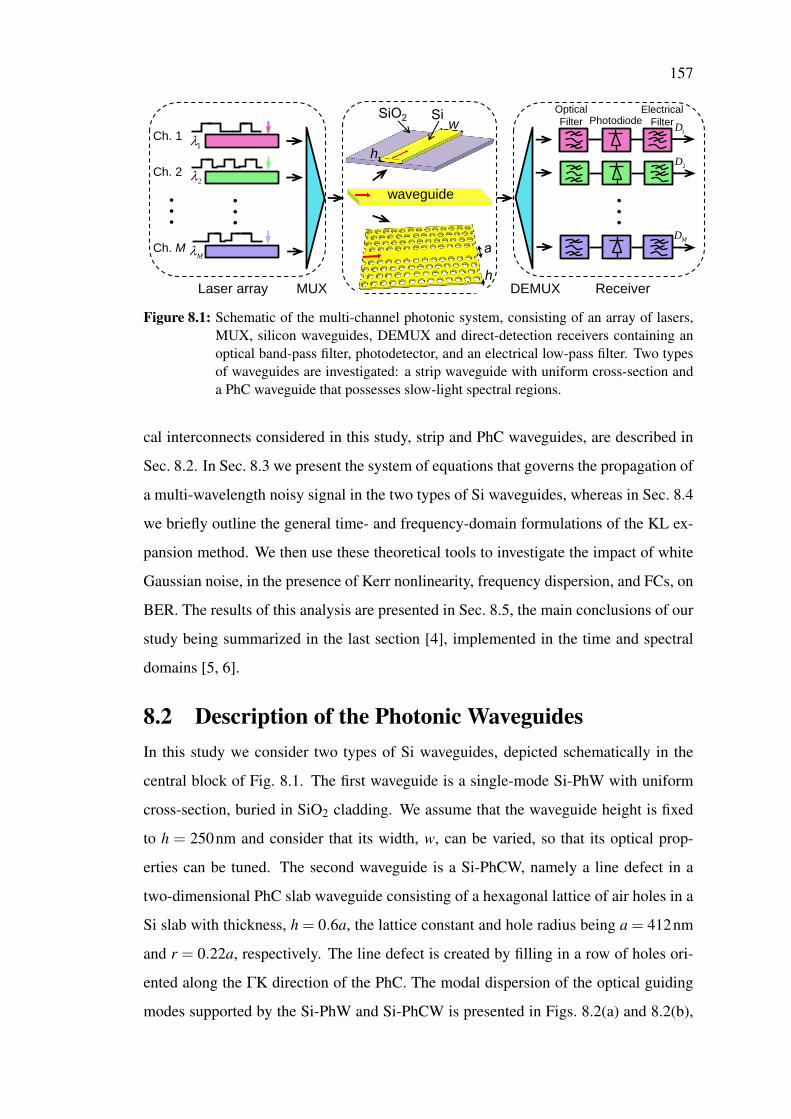
157
w
Laser array MUX
waveguide
DEMUX Receiver
…
Ch. 1
Ch. 2
Ch. M
1
2
M
…
1D
2D
MD
…
Optical
Filter PhotodiodeElectrical
Filter
Figure 8.1: Schematic of the multi-channel photonic system, consisting of an array of lasers,MUX, silicon waveguides, DEMUX and direct-detection receivers containing anoptical band-pass filter, photodetector, and an electrical low-pass filter. Two typesof waveguides are investigated: a strip waveguide with uniform cross-section anda PhC waveguide that possesses slow-light spectral regions.
cal interconnects considered in this study, strip and PhC waveguides, are described in
Sec. 8.2. In Sec. 8.3 we present the system of equations that governs the propagation of
a multi-wavelength noisy signal in the two types of Si waveguides, whereas in Sec. 8.4
we briefly outline the general time- and frequency-domain formulations of the KL ex-
pansion method. We then use these theoretical tools to investigate the impact of white
Gaussian noise, in the presence of Kerr nonlinearity, frequency dispersion, and FCs, on
BER. The results of this analysis are presented in Sec. 8.5, the main conclusions of our
study being summarized in the last section [4], implemented in the time and spectral
domains [5, 6].
8.2 Description of the Photonic WaveguidesIn this study we consider two types of Si waveguides, depicted schematically in the
central block of Fig. 8.1. The first waveguide is a single-mode Si-PhW with uniform
cross-section, buried in SiO2 cladding. We assume that the waveguide height is fixed
to h = 250nm and consider that its width, w, can be varied, so that its optical prop-
erties can be tuned. The second waveguide is a Si-PhCW, namely a line defect in a
two-dimensional PhC slab waveguide consisting of a hexagonal lattice of air holes in a
Si slab with thickness, h = 0.6a, the lattice constant and hole radius being a = 412nm
and r = 0.22a, respectively. The line defect is created by filling in a row of holes ori-
ented along the ΓK direction of the PhC. The modal dispersion of the optical guiding
modes supported by the Si-PhW and Si-PhCW is presented in Figs. 8.2(a) and 8.2(b),
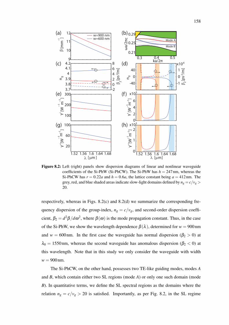
158
β [m
m−
1 ]
-40
0
40
ng
-1
0
1
x104
β2 [
ps
2/m
]
0.29
0.25
0.21
ωa/2πc
0.3 0.4 0.5ka/2π
Mode B
Mode AodA d
(b)
(c) (d)
(f )
(a)
(e)
0
2
4
6
‘
1
2
0
x103
x103
[W
−1 m
−1]
γ’
[W
−1 m
−1]
γ’’
λ [µm ] 1.52 1.56 1.6 1.64 1.68
λ [µm]
[W
−1 m
−1]
γ’
[W
−1 m
−1]
γ’’
(g) (h)
9
10
11
12
w=900 nm w=600 nm
ng
β2 [
ps
2 /m]
3.7
3.8
3.9
4
4.1
4.2
-2
0
2
4
6
8
100
200
300
20
60
100
1.52 1.56 1.6 1.64 1.68
Figure 8.2: Left (right) panels show dispersion diagrams of linear and nonlinear waveguidecoefficients of the Si-PhW (Si-PhCW). The Si-PhW has h = 247nm, whereas theSi-PhCW has r = 0.22a and h = 0.6a, the lattice constant being a = 412nm. Thegrey, red, and blue shaded areas indicate slow-light domains defined by ng = c/vg >20.
respectively, whereas in Figs. 8.2(c) and 8.2(d) we summarize the corresponding fre-
quency dispersion of the group-index, ng = c/vg, and second-order dispersion coeffi-
cient, β2 = d2β/dω2, where β (ω) is the mode propagation constant. Thus, in the case
of the Si-PhW, we show the wavelength dependence β (λ ), determined for w = 900nm
and w = 600nm. In the first case the waveguide has normal dispersion (β2 > 0) at
λ0 = 1550nm, whereas the second waveguide has anomalous dispersion (β2 < 0) at
this wavelength. Note that in this study we only consider the waveguide with width
w = 900nm.
The Si-PhCW, on the other hand, possesses two TE-like guiding modes, modes A
and B, which contain either two SL regions (mode A) or only one such domain (mode
B). In quantitative terms, we define the SL spectral regions as the domains where the
relation ng = c/vg > 20 is satisfied. Importantly, as per Fig. 8.2, in the SL regime
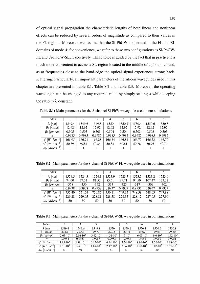
159
of optical signal propagation the characteristic lengths of both linear and nonlinear
effects can be reduced by several orders of magnitude as compared to their values in
the FL regime. Moreover, we assume that the Si-PhCW is operated in the FL and SL
domains of mode A; for convenience, we refer to these two configurations as Si-PhCW-
FL and Si-PhCW-SL, respectively. This choice is guided by the fact that in practice it is
much more convenient to access a SL region located in the middle of a photonic band,
as at frequencies close to the band-edge the optical signal experiences strong back-
scattering. Particularly, all important parameters of the silicon waveguides used in this
chapter are presented in Table 8.1, Table 8.2 and Table 8.3. Moreover, the operating
wavelength can be changed to any required value by simply scaling a while keeping
the ratio a/λ constant.
Table 8.1: Main parameters for the 8-channel Si-PhW waveguide used in our simulations.
Index 1 2 3 4 5 6 7 8λ [nm] 1549.4 1549.6 1549.8 1550 1550.2 1550.4 1550.6 1550.8
β1 [ns/m] 12.92 12.92 12.92 12.92 12.92 12.92 12.92 12.92β2 [ps2/m] 0.505 0.505 0.505 0.504 0.504 0.503 0.503 0.503
κ 0.9985 0.9985 0.9985 0.9985 0.9985 0.9985 0.9985 0.9985γ ′ [W−1m−1] 166.95 166.91 166.88 166.84 166.81 166.77 166.73 166.70γ ′′ [W−1m−1] 50.89 50.87 50.85 50.83 50.81 50.78 50.76 50.74αin [dBcm−1] 1 1 1 1 1 1 1 1
Table 8.2: Main parameters for the 8-channel Si-PhCW-FL waveguide used in our simulations.
Index 1 2 3 4 5 6 7 8λ [nm] 1524.5 1524.3 1524.1 1523.9 1523.7 1523.5 1523.2 1523.0
β1 [ns/m] 74.60 77.51 81.52 85.61 89.71 94.50 107.47 123.22β2 [ps2/m] -358 -350 -342 -333 -325 -317 -309 -302
κ 0.9938 0.9938 0.9938 0.9937 0.9937 0.9937 0.9937 0.9937γ ′ [W−1m−1] 752.40 751.64 750.87 750.11 749.35 748.58 748.03 747.88γ ′′ [W−1m−1] 229.28 229.05 228.81 228.58 228.35 228.12 227.95 227.90αin [dBcm−1] 50 50 50 50 50 50 50 50
Table 8.3: Main parameters for the 8-channel Si-PhCW-SL waveguide used in our simulations.
Index 1 2 3 4 5 6 7 8λ [nm] 1549.4 1549.6 1549.8 1550 1550.2 1550.4 1550.6 1550.8
β1 [ns/m] 29.87 29.83 29.79 29.75 29.71 29.67 29.63 29.60β2 [ps2/m] -2.63·104 -2.96·104 -3.62·104 -4.31·104 -5·104 -6.03·104 -9.6·104 -1.62·105
κ 0.9954 0.9953 0.9953 0.9953 0.9953 0.9952 0.9952 0.9951γ ′ [W−1m−1] 4.95·103 5.38·103 6.15·103 6.94·103 7.74·103 8.86·103 1.26·104 1.88·104
γ ′′ [W−1m−1] 1.51·103 1.64·103 1.87·103 2.12·103 2.36·103 2.70·103 3.82·103 5.72·103
αin [dBcm−1] 50 50 50 50 50 50 50 50
160
8.3 Theory of Multi-wavelength Optical Signal Propa-
gation in Silicon Wires
In this section, the full theoretical model in Sec. 2.6.2 is used to investigate the prop-
agation of a multi-wavelength optical signal in both Si-PhWs and Si-PhCWs. This
model rigorously describes the evolution of the optical field in the presence of FCs as
well as the dynamics of FC density. Specifically, the coupled dynamics of the opti-
cal signal and FCs are governed by Eqs. (2.21). Particularly, in Eqs. (2.21), τc is the
FC relaxation time (in our analysis we assumed τc = 0.5ns), δnfc and αfc are the FC-
induced refractive index change and FC loss coefficient, respectively, and are given by
δnfc = σnN and αfc = σαN, where N is the FC density, σα = 1.45×10⁻²¹(λ/λ0)2 (in
units of m2), and σn = σ(λ/λ0)2 (in units of m3), with σ and λ0 = 1550nm being a
power dependent coefficient [7] and a reference wavelength, respectively. Moreover,
the frequency dispersion of the real and imaginary part of the nonlinear coefficient γ is
presented in Figs. 8.2(e) through 8.2(h). As these figures illustrate, the nonlinear coef-
ficient in the case of Si-PhCWs can be more than two orders of magnitude larger than
that of Si-PhWs, being particularly large in the SL domain. In addition, in the spectral
region considered in this work γ ′ is more than 10× larger than γ ′′, which suggests that
SPM is the dominant nonlinear effect. For all multi-channel photonic systems consid-
ered in this study, we assume that the bit window is T0 = 100ps, the channel spacing
is ∆ω = 25GHz, and the reference wavelength (the wavelength of channel 1) for the
Si-PhW, Si-PhCW-FL, and Si-PhCW-SL systems is 1550nm, 1550nm, and 1523.9nm,
respectively.
The superposition of the optical signal and noise propagating in the ith channel of
a Si-PhW or Si-PhCW photonic system is selected to be:
ui(z,T ) =[√
Pi(z)+ai(z,T )]e− jΦi(z), (8.1)
where Pi(z) is the power of the CW signal in the ith channel, ai(z,T ) is the complex ad-
ditive Gaussian noise, and Φi(z) is a global phase shift associated with the ith channel.
We also assume that the noise components at the input of the waveguide are statistically
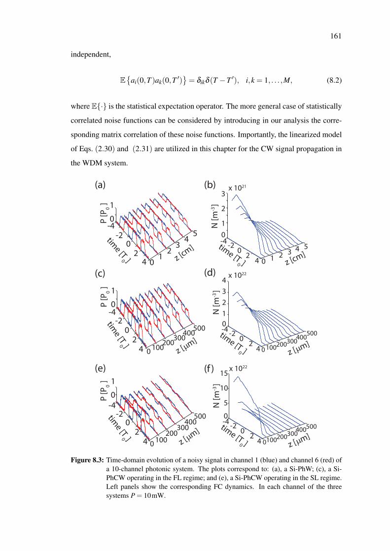
161
independent,
E
ai(0,T )ak(0,T ′)= δikδ (T −T ′), i,k = 1, . . . ,M, (8.2)
where E· is the statistical expectation operator. The more general case of statistically
correlated noise functions can be considered by introducing in our analysis the corre-
sponding matrix correlation of these noise functions. Importantly, the linearized model
of Eqs. (2.30) and (2.31) are utilized in this chapter for the CW signal propagation in
the WDM system.
01
23
45
42
0-2
-40
1
z [cm
]
time [T
0 ]
P [
P0
]
0 1 2 3 4 5
0
1
2
3x 10²¹
N [
m-3
]
42
0-2
-4tim
e [T0 ] z [cm]
0100
200300
400500
z [µm
]4
2
0
-2-40
1
time [T
0 ]
P [
P0
]
0 100200
300400
500
0
1
2
3
4x 10²²
N [
m-3
]
42
0-2
-4tim
e [T0 ] z [µ
m]
0100
200300
400500
z [µm
]
4
2
0-2
-4
0
1
time [T
0 ]
P [
P0
]
0
5
10
15x 1022
N [
m-3
]
42
0-2
-4tim
e [T0 ] 0100
200300
400500
z [µm]
(a) (b)
(c) (d)
(e) (f )
Figure 8.3: Time-domain evolution of a noisy signal in channel 1 (blue) and channel 6 (red) ofa 10-channel photonic system. The plots correspond to: (a), a Si-PhW; (c), a Si-PhCW operating in the FL regime; and (e), a Si-PhCW operating in the SL regime.Left panels show the corresponding FC dynamics. In each channel of the threesystems P = 10mW.
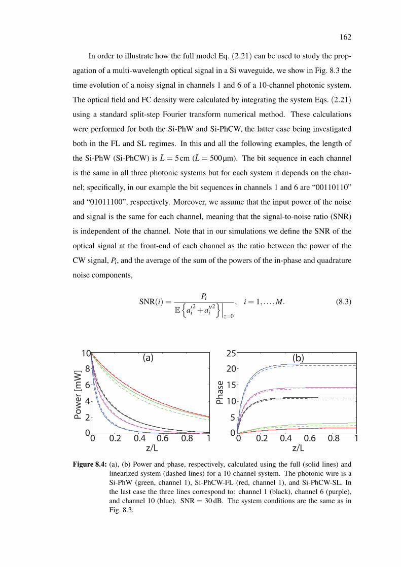
162
In order to illustrate how the full model Eq. (2.21) can be used to study the prop-
agation of a multi-wavelength optical signal in a Si waveguide, we show in Fig. 8.3 the
time evolution of a noisy signal in channels 1 and 6 of a 10-channel photonic system.
The optical field and FC density were calculated by integrating the system Eqs. (2.21)
using a standard split-step Fourier transform numerical method. These calculations
were performed for both the Si-PhW and Si-PhCW, the latter case being investigated
both in the FL and SL regimes. In this and all the following examples, the length of
the Si-PhW (Si-PhCW) is L = 5cm (L = 500µm). The bit sequence in each channel
is the same in all three photonic systems but for each system it depends on the chan-
nel; specifically, in our example the bit sequences in channels 1 and 6 are “00110110”
and “01011100”, respectively. Moreover, we assume that the input power of the noise
and signal is the same for each channel, meaning that the signal-to-noise ratio (SNR)
is independent of the channel. Note that in our simulations we define the SNR of the
optical signal at the front-end of each channel as the ratio between the power of the
CW signal, Pi, and the average of the sum of the powers of the in-phase and quadrature
noise components,
SNR(i) =Pi
E
a′i2+a′′i
2∣∣∣
z=0
, i = 1, . . . ,M. (8.3)
0 0.2 0.4 0.6 0.8 10
2
4
6
8
10
z/L
Po
we
r [m
W]
(a)
0 0.2 0.4 0.6 0.8 10
5
10
15
20
25
z/L
Ph
ase
(b)
Figure 8.4: (a), (b) Power and phase, respectively, calculated using the full (solid lines) andlinearized system (dashed lines) for a 10-channel system. The photonic wire is aSi-PhW (green, channel 1), Si-PhCW-FL (red, channel 1), and Si-PhCW-SL. Inthe last case the three lines correspond to: channel 1 (black), channel 6 (purple),and channel 10 (blue). SNR = 30 dB. The system conditions are the same as inFig. 8.3.
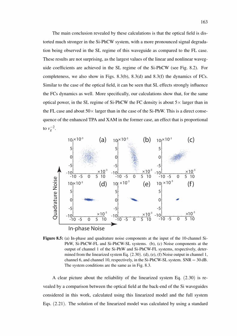
163
The main conclusion revealed by these calculations is that the optical field is dis-
torted much stronger in the Si-PhCW system, with a more pronounced signal degrada-
tion being observed in the SL regime of this waveguide as compared to the FL case.
These results are not surprising, as the largest values of the linear and nonlinear waveg-
uide coefficients are achieved in the SL regime of the Si-PhCW (see Fig. 8.2). For
completeness, we also show in Figs. 8.3(b), 8.3(d) and 8.3(f) the dynamics of FCs.
Similar to the case of the optical field, it can be seen that SL effects strongly influence
the FCs dynamics as well. More specifically, our calculations show that, for the same
optical power, in the SL regime of Si-PhCW the FC density is about 5× larger than in
the FL case and about 50× larger than in the case of the Si-PhW. This is a direct conse-
quence of the enhanced TPA and XAM in the former case, an effect that is proportional
to v−2g .
Qu
ad
ratu
re N
ois
e
×10-3
-5
0
5
×10-3
×10-3
-5
0
5
×10-3
-5 0 5
×10-3
-5
0
5
×10-3
×10-3
-5
0
5
×10-3
×10-3
-5
0
5
×10-3
-5 0 5
×10-3
-5
0
5
×10-3
In-phase Noise
10
10
10
10 10
1010
10-10-10
-10-10-10-10
-10-10-5 0 5 10-10
-5 0 5 10-10-5 0 5 10-10
-5 0 5 10-10
(a) (b) (c)
(e)(d) (f )
Figure 8.5: (a) In-phase and quadrature noise components at the input of the 10-channel Si-PhW, Si-PhCW-FL and Si-PhCW-SL systems. (b), (c) Noise components at theoutput of channel 1 of the Si-PhW and Si-PhCW-FL systems, respectively, deter-mined from the linearized system Eq. (2.30). (d), (e), (f) Noise output in channel 1,channel 6, and channel 10, respectively, in the Si-PhCW-SL system. SNR = 30 dB.The system conditions are the same as in Fig. 8.3.
A clear picture about the reliability of the linearized system Eq. (2.30) is re-
vealed by a comparison between the optical field at the back-end of the Si waveguides
considered in this work, calculated using this linearized model and the full system
Eqs. (2.21). The solution of the linearized model was calculated by using a standard
164
5th order Runge-Kutta method. The conclusions of such a comparison are summarized
in Fig. 8.4, where we plot the evolution of the optical power and phase of a multi-
wavelength optical signal corresponding to three different regimes of propagation in
Si waveguides. In particular, we considered the same 10-channels system as above,
the three waveguides being a Si-PhW, a Si-PhCW-FL, and a Si-PhCW-SL. The first
conclusion we can derive from the results presented in Fig. 8.4 is that for all systems
and all channels the linearized system describes fairly accurately the dynamics of the
optical field.
Our simulations show that in the case of the Si-PhW and Si-PhCW-FL systems the
power and phase of the optical signal are nearly the same across all 10 channels and as
such we plot in Fig. 8.4 only the quantities that correspond to channel 1. This is an ex-
pected result because in these two cases the linear and nonlinear waveguide coefficients
are only weakly dispersive, so that in the case of small inter-channel separation they do
not vary much from channel to channel. This picture changes markedly if one con-
siders the case of the Si-PhCW-SL system. Thus, in the SL regime, as a consequence
of SL effects, the waveguide coefficients are enhanced and become much more disper-
sive. This results in a large spread of the values of the parameters that characterize the
propagation of optical signals in the SL multi-channel system.
The linearized system Eq. (2.30) also allows one to determine the evolution of the
noise components of the optical field. This is illustrated in Fig. 8.5, where we present
the noise components at the back-end of the Si waveguides investigated above. Note
that in this figure we plot ai(z, t)e− jΦi(z), calculated at z = L = 5cm and z = L = 500µm
for the Si-PhW and Si-PhCW systems, respectively, where Φi(z) is the phase defined
by Eq. (8.1). The statistical properties of the input additive white Gaussian noise do not
depend on the channel nor the particular system considered. Comparing Figs. 8.5(b)
and 8.5(c), which correspond to channel 1 of the Si-PhW and Si-PhCW-FL systems,
respectively, it can be seen that our model predicts a larger parametric amplification of
the quadrature noise. Moreover, the output noise in channel 1, channel 6, and channel
10 of the Si-PhCW-SL system is shown in Figs. 8.5(d), 8.5(e), and 8.5(f), respectively.
Interestingly enough, it can be seen not only that, similar to the case of the optical
signal, there is a large noise variation with the transmission channel, but also that the
noise amplitude rapidly decreases with the channel number. This latter dependence is
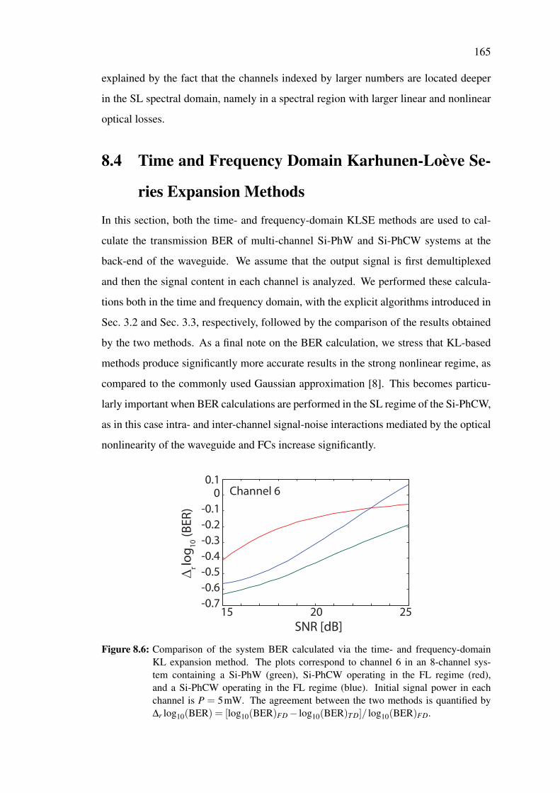
165
explained by the fact that the channels indexed by larger numbers are located deeper
in the SL spectral domain, namely in a spectral region with larger linear and nonlinear
optical losses.
8.4 Time and Frequency Domain Karhunen-Loeve Se-
ries Expansion Methods
In this section, both the time- and frequency-domain KLSE methods are used to cal-
culate the transmission BER of multi-channel Si-PhW and Si-PhCW systems at the
back-end of the waveguide. We assume that the output signal is first demultiplexed
and then the signal content in each channel is analyzed. We performed these calcula-
tions both in the time and frequency domain, with the explicit algorithms introduced in
Sec. 3.2 and Sec. 3.3, respectively, followed by the comparison of the results obtained
by the two methods. As a final note on the BER calculation, we stress that KL-based
methods produce significantly more accurate results in the strong nonlinear regime, as
compared to the commonly used Gaussian approximation [8]. This becomes particu-
larly important when BER calculations are performed in the SL regime of the Si-PhCW,
as in this case intra- and inter-channel signal-noise interactions mediated by the optical
nonlinearity of the waveguide and FCs increase significantly.
15 20 25-0.7
-0.6
-0.5
-0.4
-0.3
-0.2
-0.1
00.1
SNR [dB]
Channel 6
∆rlo
g1
0 (
BE
R)
Figure 8.6: Comparison of the system BER calculated via the time- and frequency-domainKL expansion method. The plots correspond to channel 6 in an 8-channel sys-tem containing a Si-PhW (green), Si-PhCW operating in the FL regime (red),and a Si-PhCW operating in the FL regime (blue). Initial signal power in eachchannel is P = 5mW. The agreement between the two methods is quantified by∆r log10(BER) = [log10(BER)FD− log10(BER)T D]/ log10(BER)FD.
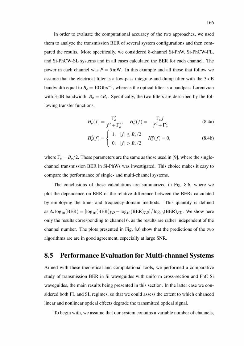
166
In order to evaluate the computational accuracy of the two approaches, we used
them to analyze the transmission BER of several system configurations and then com-
pared the results. More specifically, we considered 8-channel Si-PhW, Si-PhCW-FL,
and Si-PhCW-SL systems and in all cases calculated the BER for each channel. The
power in each channel was P = 5mW. In this example and all those that follow we
assume that the electrical filter is a low-pass integrate-and-dump filter with the 3-dB
bandwidth equal to Be = 10Gbs−1, whereas the optical filter is a bandpass Lorentzian
with 3-dB bandwidth, Bo = 4Be. Specifically, the two filters are described by the fol-
lowing transfer functions,
H io( f ) =
Γ2o
f 2 +Γ2o, Hq
o ( f ) =− Γo ff 2 +Γ2
o, (8.4a)
H ie( f ) =
1, | f | ≤ Be/2
0, | f |> Be/2Hq
e ( f ) = 0, (8.4b)
where Γo = Bo/2. These parameters are the same as those used in [9], where the single-
channel transmission BER in Si-PhWs was investigated. This choice makes it easy to
compare the performance of single- and multi-channel systems.
The conclusions of these calculations are summarized in Fig. 8.6, where we
plot the dependence on BER of the relative difference between the BERs calculated
by employing the time- and frequency-domain methods. This quantity is defined
as ∆r log10(BER) = [log10(BER)FD− log10(BER)T D]/ log10(BER)FD. We show here
only the results corresponding to channel 6, as the results are rather independent of the
channel number. The plots presented in Fig. 8.6 show that the predictions of the two
algorithms are are in good agreement, especially at large SNR.
8.5 Performance Evaluation for Multi-channel SystemsArmed with these theoretical and computational tools, we performed a comparative
study of transmission BER in Si waveguides with uniform cross-section and PhC Si
waveguides, the main results being presented in this section. In the latter case we con-
sidered both FL and SL regimes, so that we could assess the extent to which enhanced
linear and nonlinear optical effects degrade the transmitted optical signal.
To begin with, we assume that our system contains a variable number of channels,
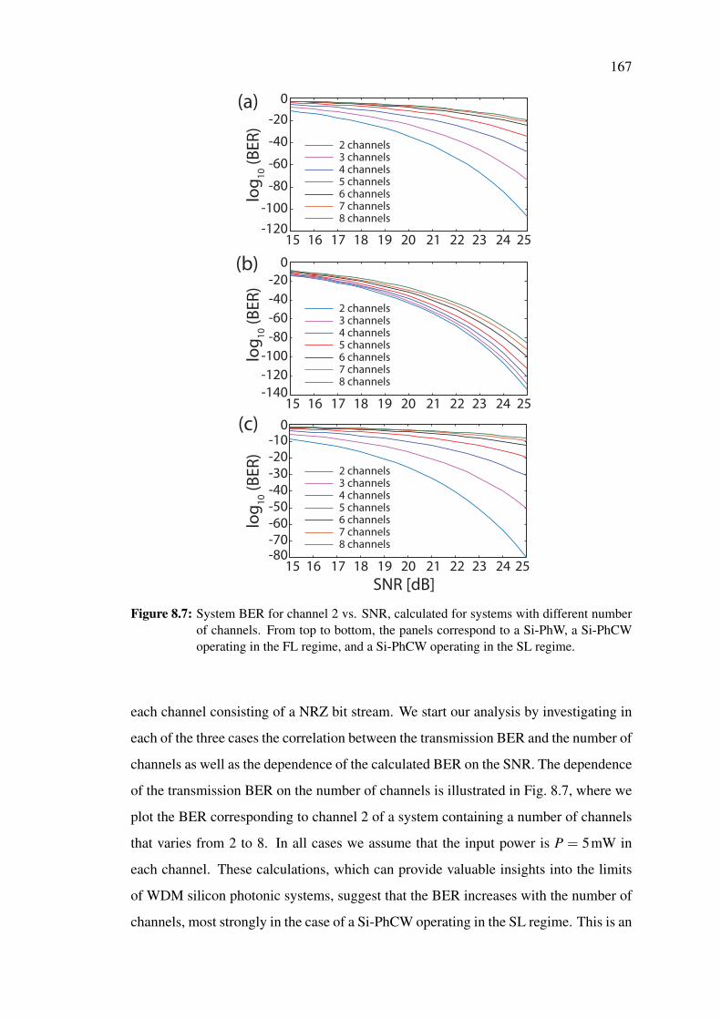
167
15 16 17 18 19 20 21 22 23 24 25-120
-100
-80
-60
-40
-20
0
2 channels3 channels4 channels5 channels6 channels7 channels8 channels
log
10 (
BE
R)
-140
-120
-100
-80
-60
-40
-20
0
15 16 17 18 19 20 21 22 23 24 25
2 channels3 channels4 channels5 channels6 channels7 channels8 channels
-80-70
-60
-50
-40
-30
-20
-100
15 16 17 18 19 20 21 22 23 24 25
SNR [dB]
2 channels3 channels4 channels5 channels6 channels7 channels8 channels
(a)
(b)
(c)
log
10 (
BE
R)
log
10 (
BE
R)
Figure 8.7: System BER for channel 2 vs. SNR, calculated for systems with different numberof channels. From top to bottom, the panels correspond to a Si-PhW, a Si-PhCWoperating in the FL regime, and a Si-PhCW operating in the SL regime.
each channel consisting of a NRZ bit stream. We start our analysis by investigating in
each of the three cases the correlation between the transmission BER and the number of
channels as well as the dependence of the calculated BER on the SNR. The dependence
of the transmission BER on the number of channels is illustrated in Fig. 8.7, where we
plot the BER corresponding to channel 2 of a system containing a number of channels
that varies from 2 to 8. In all cases we assume that the input power is P = 5mW in
each channel. These calculations, which can provide valuable insights into the limits
of WDM silicon photonic systems, suggest that the BER increases with the number of
channels, most strongly in the case of a Si-PhCW operating in the SL regime. This is an
168
expected conclusion because as the number of channels increases the strength of inter-
channel interactions mediated by optical nonlinearity and FCs increases, which results
in a degradation of the system performance. Moreover, as linear and nonlinear optical
effects are enhanced in the SL regime, a more pronounced deterioration of the system
performance is observed in this case. Last but not least, the influence of number of
channels would be extremely small in systems where a Si waveguide is not contained,
under the assumption that neither the receivers or the DEMUX would induce noise.
Thus, when considering the BER performance in this case, one can refer to the BER
plots for single-channel back-to-back system configuration, as shown in Fig. 4.2(a).
Po
we
r [m
W]
15 20 252
4
6
8
10
-20
-16
-12
-8
-4
15 20 252
4
6
8
10
-20
-16
-12
-8
-4
Po
we
r [m
W]
15 20 252
4
6
8
10
-20
-16
-12
-8
-4
15 20 252
4
6
8
10
-20
-16
-12
-8
-4
SNR [dB]
Po
we
r [m
W]
15 20 252
4
6
8
10
-20
-16
-12
-8
-4
(a) (b)
(c) (d)
(e)
SNR [dB]
15 20 252
4
6
8
10
-20
-16
-12
-8
-4(f)
Figure 8.8: Maps of log10(BER) vs. power and SNR, calculated for three different 8-channelsystems: from top to bottom, the panels correspond to a Si-PhW, a Si-PhCW op-erating in the FL regime, and a Si-PhCW operating in the SL regime. Left andright panels correspond to channel 1 and channel 8, respectively. Black curvescorrespond to log10(BER) =−9.
The physical parameter that most critically affects the system performance is the
optical power of the signal. Indeed, the optical field induces nonlinear effects that affect
the signal propagation in the Si waveguide and generates FCs that modify the optical
properties of the waveguide. Therefore, in the next part of our study, we investigate the
dependence of the performance of the 8-channel system described above on the opti-
cal power contained in each channel, at the front-end of the three type of waveguides
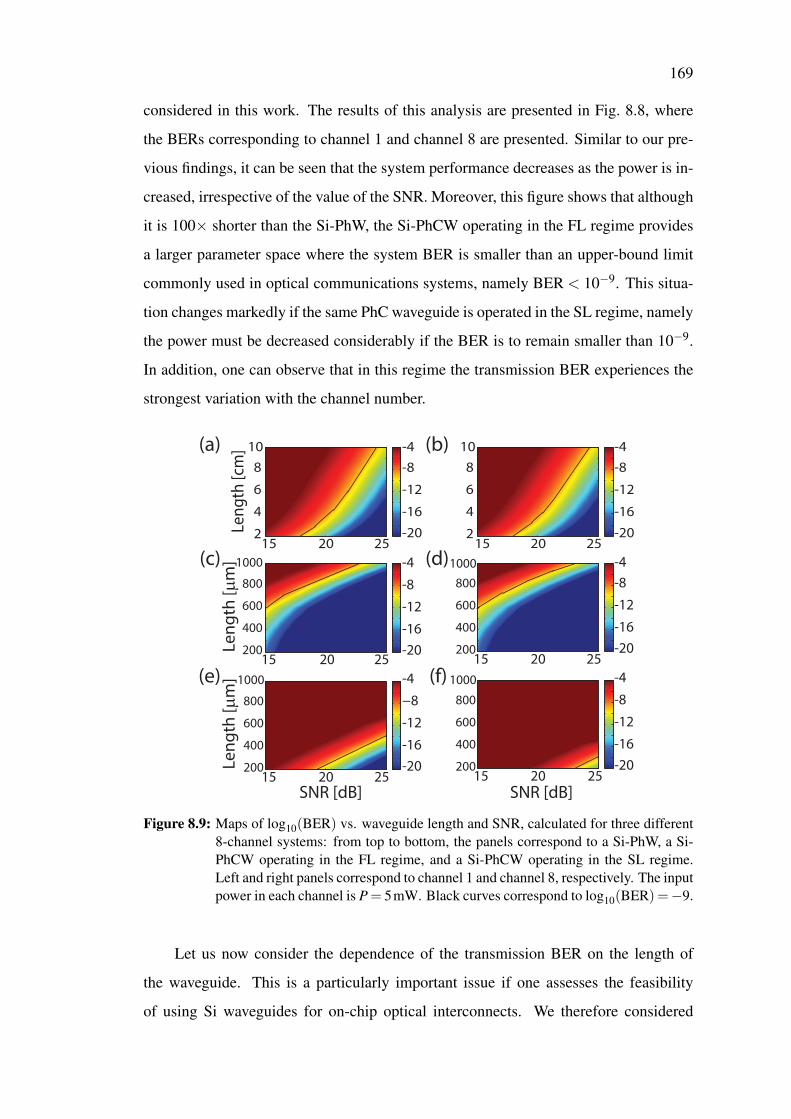
169
considered in this work. The results of this analysis are presented in Fig. 8.8, where
the BERs corresponding to channel 1 and channel 8 are presented. Similar to our pre-
vious findings, it can be seen that the system performance decreases as the power is in-
creased, irrespective of the value of the SNR. Moreover, this figure shows that although
it is 100× shorter than the Si-PhW, the Si-PhCW operating in the FL regime provides
a larger parameter space where the system BER is smaller than an upper-bound limit
commonly used in optical communications systems, namely BER < 10−9. This situa-
tion changes markedly if the same PhC waveguide is operated in the SL regime, namely
the power must be decreased considerably if the BER is to remain smaller than 10−9.
In addition, one can observe that in this regime the transmission BER experiences the
strongest variation with the channel number.
Len
gth
[cm
]
15 20 252
4
6
8
10
-20
-16
-12
-8
-4
15 20 252
4
6
8
10
-20
-16
-12
-8
-4
Le
ng
th [µ
m]
15 20 25200
400
600
800
1000
-20
-16
-12
-8
-4
15 20 25200
400
600
800
1000
-20
-16
-12
-8
-4
SNR [dB]
15 20 25200
400
600
800
1000
-20
-16
-12
−8
-4
SNR [dB]
15 20 25200
400
600
800
1000
-20
-16
-12
-8
-4
(a) (b)
(c)
(e)
(d)
(f)
Le
ng
th [µ
m]
Figure 8.9: Maps of log10(BER) vs. waveguide length and SNR, calculated for three different8-channel systems: from top to bottom, the panels correspond to a Si-PhW, a Si-PhCW operating in the FL regime, and a Si-PhCW operating in the SL regime.Left and right panels correspond to channel 1 and channel 8, respectively. The inputpower in each channel is P= 5mW. Black curves correspond to log10(BER) =−9.
Let us now consider the dependence of the transmission BER on the length of
the waveguide. This is a particularly important issue if one assesses the feasibility
of using Si waveguides for on-chip optical interconnects. We therefore considered
170
Si-PhWs and Si-PhCWs with different length but in order to be able to compare the
findings of this investigation to the conclusions drawn so far we assumed that the ratio
of the lengths of the two waveguides is fixed to 100. The system BER determined
under these circumstances, for the same 8-channel system and power P = 5mW, is
plotted in Fig. 8.9. One important result illustrated by this figure is that, among the
three cases investigated, the Si-PhCW operated in the FL regime provides the optimum
performance. When the same waveguide is operated in the SL regime, on the other
hand, the BER is larger than the threshold of 10−9 in almost the entire parameter space
considered in Fig. 8.9.
8.6 ConclusionIn conclusion, we have presented a comprehensive analysis of bit-error rates in multi-
channel photonic systems containing silicon waveguides. We have considered two
types of such photonic devices, namely a strip waveguide with uniform cross-section
and a photonic crystal waveguide. The latter photonic waveguide allowed us to ex-
tend our analysis to the important case of slow-light propagation where both linear
and nonlinear optical effects are enhanced. Our calculations of the bit-error rate have
demonstrated that using photonic crystal waveguides in the fast light regime allows one
to reduce the device footprint by as much as two orders of magnitude while maintaining
the system performance to an almost unchanged level. However, if the photonic crystal
is operated in the slow-light regime at similar power levels, a significant degradation of
the system performance is observed.
The theoretical formalism introduced in this study can also be applied to other,
more complex devices of practical interest. For example, our theoretical approach
can be applied to taper, slot and other types of waveguides by simply using the cor-
responding linear and nonlinear waveguide optical coefficients. Moreover, after prop-
erly modifying the system of equations governing the optical field dynamics in silicon
waveguides, a similar theoretical formalism can be employed to study the transmission
bit-error rate of photonic systems containing, e.g, splitters, ring modulators coupled
to a waveguide, and multi-mode waveguides. Equally important, the generality of the
theoretical methods used in this study makes it easy to adapt them to tackle much more
advanced signal modulation formats and detection schemes than those considered in

171
this chapter.
In the next chapter, the research emphasis will shift to the single-channel silicon
photonic interconnect that operating in the pulsed regime.
172
Bibliography[1] X. Chen, N. C. Panoiu, and R. M. Osgood, “Theory of Raman-mediated pulsed
amplification in silicon-wire waveguides,” IEEE J. Quantum Electron. 42, 160-
170 (2006).
[2] N. C. Panoiu, J. F. McMillan, and C. W. Wong, “Theoretical analysis of pulse dy-
namics in silicon photonic crystal wire waveguides,” IEEE J. Sel. Top. Quantum
Electron. 16, 257-266 (2010).
[3] S. Lavdas and N. C. Panoiu, “Theory of Pulsed Four-Wave-Mixing in One-
dimensional Silicon Photonic Crystal Slab Waveguides,” Phys. Rev. B 93, 115435
(2016).
[4] A. Papoulis, Probability, Random Variables, and Stochastic Processes 3rd ed,
(McGraw-Hill, New York, 1991).
[5] A. Mafi and S. Raghavan, “Nonlinear phase noise in optical communication sys-
tems using eigenfunction expansion method,” Opt. Eng. 50, 055003 (2011).
[6] E. Forestieri and M. Secondini, “On the Error Probability Evaluation in Lightwave
Systems With Optical Amplification,” IEEE J. Lightwave Technol. 27, 706-717
(2009).
[7] Q. Lin, O. J. Painter, and G. P. Agrawal, “Nonlinear optical phenomena in silicon
waveguides: Modeling and applications,” Opt. Express 15, 16604-16644 (2007).
[8] G. Bosco, A. Carena, V. Curri, R. Gaudino, P. Poggiolini, and S. Benedetto, “A
novel analytical approach to the evaluation of the impact of fiber parametric gain
on the bit error rate,” IEEE Trans. Commun. 49, 2154-2163 (2001).
[9] J. You and N. C. Panoiu, “Calculation of Bit Error Rates in Optical Systems with
Silicon Photonic Wires,” IEEE J. Quantum Electron. 51, 8400108 (2015).
Chapter 9
Single-channel Silicon Photonic
Interconnects Utilizing RZ Pulsed
Signals
9.1 IntroductionIn this chapter, we analyze the transmission BER in single-channel Si photonic systems
operated in the RZ regime. The photonic systems investigated in this study consist of
an optical transmitter, a Si optical waveguide, and a direct-detection receiver, as shown
in Fig. 9.1. The optical link can be either a single-mode Si-PhW with uniform cross-
section or a Si-PhCW, and is connected to a direct-detection receiver consisting of a
Lorentzian bandpass optical filter, an ideal square-law photodetector, and an integrate-
and-dump low-pass electrical filter. An ON-OFF keying (OOK) modulated Gaussian
pulses with a 512-bit pseudorandom binary sequence (PRBS) pattern, together with
complex additive white noise, form the input signal. To characterize the pulse dynam-
ics upon transmission, we use a theoretical model, which incorporates all the signifi-
cant optical effects, including the linear loss, GV dispersion (GVD), free-carrier (FC)
dispersion (FCD), FC absorption (FCA), self-phase modulation (SPM), two-photon ab-
sorption (TPA), and the mutual interaction between the FCs and the optical field [1–4].
Moreover, the Fourier-series Karhunen-Loeve (KL) expansion approach is employed
in conjunction with a perturbation theory for the calculation of the noise covariance
matrix [5], to evaluate the system BER at the back-end of the receiver.
The rest of the chapter is organized as follows. The rigorous theoretical model that
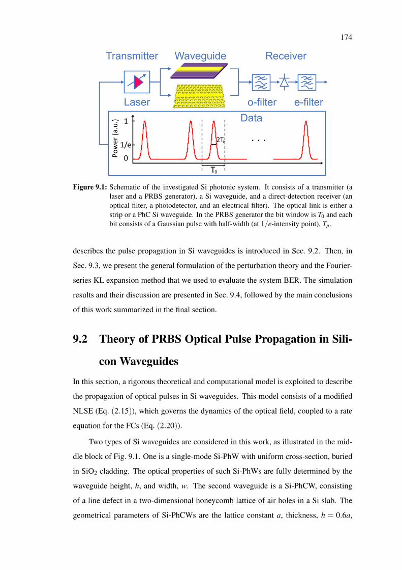
174
Laser o-filter e-filter
Waveguide ReceiverTransmitter
Data
0
1
1/e
Pow
er (a
.u.)
2Tp
T0
. . .
Figure 9.1: Schematic of the investigated Si photonic system. It consists of a transmitter (alaser and a PRBS generator), a Si waveguide, and a direct-detection receiver (anoptical filter, a photodetector, and an electrical filter). The optical link is either astrip or a PhC Si waveguide. In the PRBS generator the bit window is T0 and eachbit consists of a Gaussian pulse with half-width (at 1/e-intensity point), Tp.
describes the pulse propagation in Si waveguides is introduced in Sec. 9.2. Then, in
Sec. 9.3, we present the general formulation of the perturbation theory and the Fourier-
series KL expansion method that we used to evaluate the system BER. The simulation
results and their discussion are presented in Sec. 9.4, followed by the main conclusions
of this work summarized in the final section.
9.2 Theory of PRBS Optical Pulse Propagation in Sili-
con Waveguides
In this section, a rigorous theoretical and computational model is exploited to describe
the propagation of optical pulses in Si waveguides. This model consists of a modified
NLSE (Eq. (2.15)), which governs the dynamics of the optical field, coupled to a rate
equation for the FCs (Eq. (2.20)).
Two types of Si waveguides are considered in this work, as illustrated in the mid-
dle block of Fig. 9.1. One is a single-mode Si-PhW with uniform cross-section, buried
in SiO2 cladding. The optical properties of such Si-PhWs are fully determined by the
waveguide height, h, and width, w. The second waveguide is a Si-PhCW, consisting
of a line defect in a two-dimensional honeycomb lattice of air holes in a Si slab. The
geometrical parameters of Si-PhCWs are the lattice constant a, thickness, h = 0.6a,
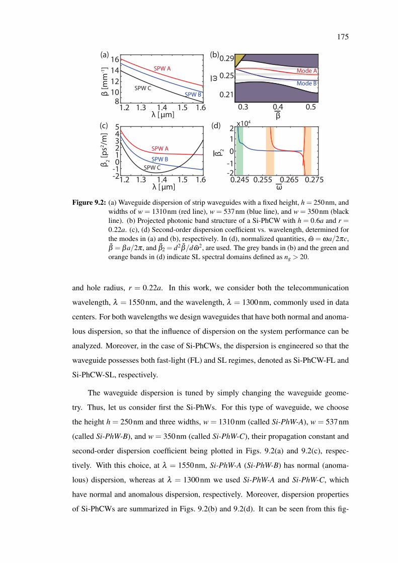
175
1.2 1.3 1.4 1.5 1.6λ [ µm]
10
12
14
16
β [
mm
-1]
0.29
0.25
0.21
0.3 0.4 0.5
Mode A
Mode B
(b)(a)
-2-1012345
1.2 1.3 1.4 1.5 1.6λ [ µm]
β2 [
ps2
/m]
-2
-1
0
1
2x10⁴
β2
0.245 0.255 0.265 0.275ω
(c) (d)
ω
β
8SPW B
SPW A
SPW C
SPW B
SPW A
SPW C
Figure 9.2: (a) Waveguide dispersion of strip waveguides with a fixed height, h = 250nm, andwidths of w = 1310nm (red line), w = 537nm (blue line), and w = 350nm (blackline). (b) Projected photonic band structure of a Si-PhCW with h = 0.6a and r =0.22a. (c), (d) Second-order dispersion coefficient vs. wavelength, determined forthe modes in (a) and (b), respectively. In (d), normalized quantities, ω = ωa/2πc,β = βa/2π , and β2 = d2β/dω2, are used. The grey bands in (b) and the green andorange bands in (d) indicate SL spectral domains defined as ng > 20.
and hole radius, r = 0.22a. In this work, we consider both the telecommunication
wavelength, λ = 1550nm, and the wavelength, λ = 1300nm, commonly used in data
centers. For both wavelengths we design waveguides that have both normal and anoma-
lous dispersion, so that the influence of dispersion on the system performance can be
analyzed. Moreover, in the case of Si-PhCWs, the dispersion is engineered so that the
waveguide possesses both fast-light (FL) and SL regimes, denoted as Si-PhCW-FL and
Si-PhCW-SL, respectively.
The waveguide dispersion is tuned by simply changing the waveguide geome-
try. Thus, let us consider first the Si-PhWs. For this type of waveguide, we choose
the height h = 250nm and three widths, w = 1310nm (called Si-PhW-A), w = 537nm
(called Si-PhW-B), and w = 350nm (called Si-PhW-C), their propagation constant and
second-order dispersion coefficient being plotted in Figs. 9.2(a) and 9.2(c), respec-
tively. With this choice, at λ = 1550nm, Si-PhW-A (Si-PhW-B) has normal (anoma-
lous) dispersion, whereas at λ = 1300nm we used Si-PhW-A and Si-PhW-C, which
have normal and anomalous dispersion, respectively. Moreover, dispersion properties
of Si-PhCWs are summarized in Figs. 9.2(b) and 9.2(d). It can be seen from this fig-
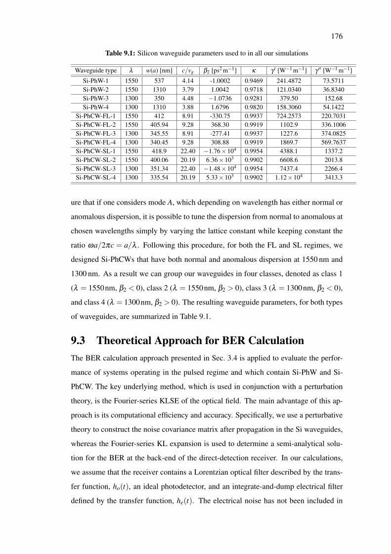
176
Table 9.1: Silicon waveguide parameters used to in all our simulations
Waveguide type λ w(a) [nm] c/vg β2 [ps2 m−1] κ γ ′ [W−1 m−1] γ ′′ [W−1 m−1]
Si-PhW-1 1550 537 4.14 -1.0002 0.9469 241.4872 73.5711Si-PhW-2 1550 1310 3.79 1.0042 0.9718 121.0340 36.8340Si-PhW-3 1300 350 4.48 −1.0736 0.9281 379.50 152.68Si-PhW-4 1300 1310 3.88 1.6796 0.9820 158.3060 54.1422
Si-PhCW-FL-1 1550 412 8.91 -330.75 0.9937 724.2573 220.7031Si-PhCW-FL-2 1550 405.94 9.28 368.30 0.9919 1102.9 336.1006Si-PhCW-FL-3 1300 345.55 8.91 -277.41 0.9937 1227.6 374.0825Si-PhCW-FL-4 1300 340.45 9.28 308.88 0.9919 1869.7 569.7637Si-PhCW-SL-1 1550 418.9 22.40 −1.76×10⁴ 0.9954 4388.1 1337.2Si-PhCW-SL-2 1550 400.06 20.19 6.36×10³ 0.9902 6608.6 2013.8Si-PhCW-SL-3 1300 351.34 22.40 −1.48×10⁴ 0.9954 7437.4 2266.4Si-PhCW-SL-4 1300 335.54 20.19 5.33×10³ 0.9902 1.12×10⁴ 3413.3
ure that if one considers mode A, which depending on wavelength has either normal or
anomalous dispersion, it is possible to tune the dispersion from normal to anomalous at
chosen wavelengths simply by varying the lattice constant while keeping constant the
ratio ωa/2πc = a/λ . Following this procedure, for both the FL and SL regimes, we
designed Si-PhCWs that have both normal and anomalous dispersion at 1550 nm and
1300 nm. As a result we can group our waveguides in four classes, denoted as class 1
(λ = 1550nm, β2 < 0), class 2 (λ = 1550nm, β2 > 0), class 3 (λ = 1300nm, β2 < 0),
and class 4 (λ = 1300nm, β2 > 0). The resulting waveguide parameters, for both types
of waveguides, are summarized in Table 9.1.
9.3 Theoretical Approach for BER CalculationThe BER calculation approach presented in Sec. 3.4 is applied to evaluate the perfor-
mance of systems operating in the pulsed regime and which contain Si-PhW and Si-
PhCW. The key underlying method, which is used in conjunction with a perturbation
theory, is the Fourier-series KLSE of the optical field. The main advantage of this ap-
proach is its computational efficiency and accuracy. Specifically, we use a perturbative
theory to construct the noise covariance matrix after propagation in the Si waveguides,
whereas the Fourier-series KL expansion is used to determine a semi-analytical solu-
tion for the BER at the back-end of the direct-detection receiver. In our calculations,
we assume that the receiver contains a Lorentzian optical filter described by the trans-
fer function, ho(t), an ideal photodetector, and an integrate-and-dump electrical filter
defined by the transfer function, he(t). The electrical noise has not been included in
177
the receiver model, a reasonable approximation considering that the electrical noise is
much smaller than the accumulated noise in the waveguide. Here, the bit-rate and bit
window are denoted as Br and T0, respectively.
9.4 Results and DiscussionIn this section, we present the results of a comprehensive performance analysis of sys-
tems containing the two types of Si waveguides. To begin with, we describe the com-
putational setup of our numerical simulations. Thus, we utilize a PRBS of Gaussian-
shaped pulses containing 29−1 bits together with a zero bit, which includes all possible
9-bit sequence patterns. The average power of the optical pulse is P = 10mW, with the
relation between the peak power, P0, and the average power per gaussian pulse being
PT0 =√
πP0Tp. The waveguide length for Si-PhWs, Si-PhCW-FLs, and Si-PhCW-SLs
is L = 5cm, L = 500µm, and L = 250µm, respectively, unless otherwise is specified.
Moreover, the number of frequency points used within one bit is 2Q+1 = 201, which
is relatively small as compared to the number of temporal sampling points, N = 1024,
within the same bit, whereas the bit-rate and signal pulse width are chosen according
to the following rules: i) When different values of the bit-rate, Br, are used, the pulse
width is fixed at Tp = 9ps. ii) When the duty-cycle dcycle = Tp× (2Br) is varied, the
signal bit-rate is kept unchanged at Br = 10Gb/s. Note that when keeping constant the
average power, P, the smaller the Br (dcycle) is, the larger the peak power P0 of a pulse
is. Moreover, in the BER calculations, we select fixed detection thresholds for each
type of Si waveguides.
A clear picture of the signal dynamics in the optical and electrical domains is
provided by Fig. 9.3, where we show the amplitude of Gaussian pulses at the output of
different types of Si waveguides, normalized to the input amplitude (left panels), and
the eye diagrams of the electrical signal after the direct-detection receiver determined
for class 1 (λ = 1550nm and β2 < 0) waveguides (right panels). As different types of
Si-PhWs and Si-PhCWs have been considered in these simulations, Fig. 9.3 illustrates
how the waveguide parameters influence the output signal. One main finding is that the
signal degradation is larger in the anomalous dispersion regime for Si-PhWs and Si-
PhCW-SLs as compared to normal dispersion regime, whereas the opposite is true in Si-
PhCW-FLs, as per Figs. 9.3(a), 9.3(c), and 9.3(e). This is explained by the magnitude
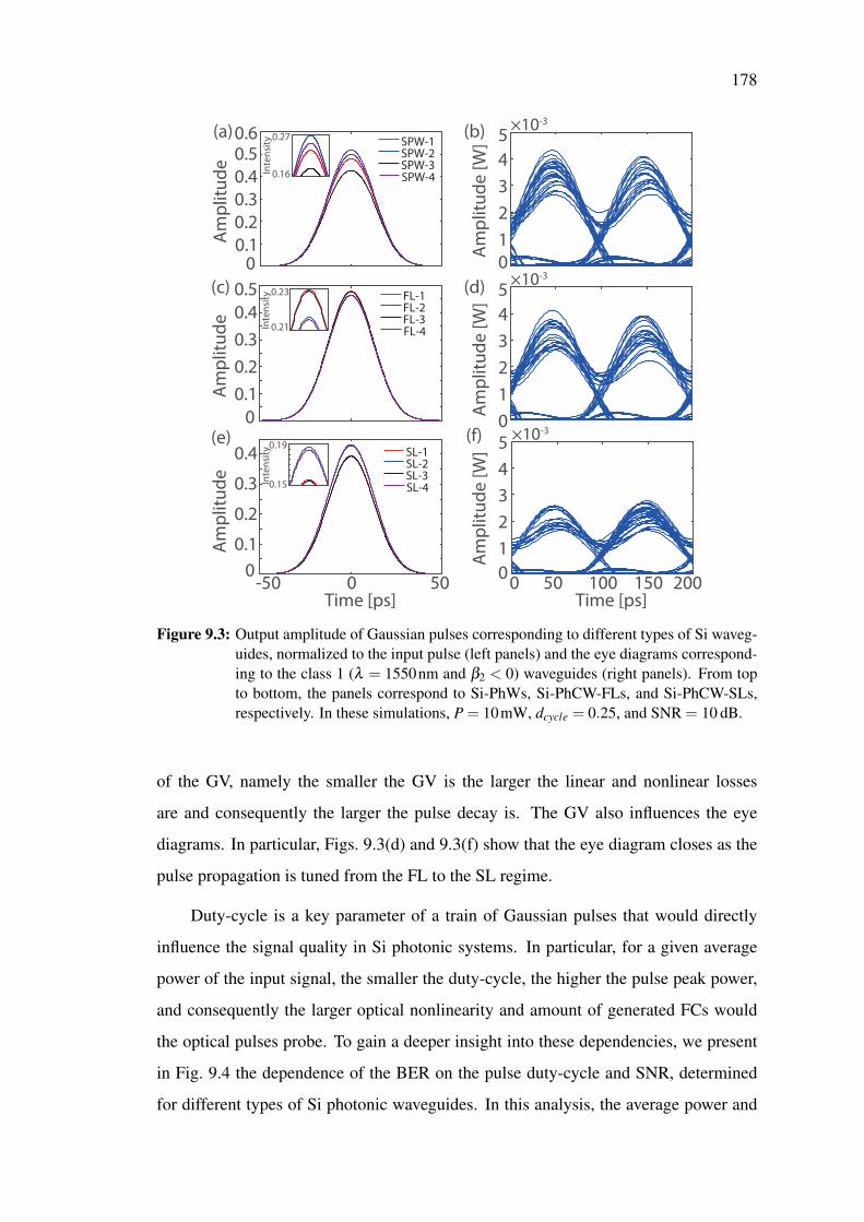
178
(a)
(c)
(e)
(b)
(d)
(f)
00.1
0.2
0.3
0.4
0.50.6
Am
plit
ud
e
0
0.1
0.2
0.3
0.4
0.5
Am
plit
ud
e
-50 50Time [ps]
0
0.1
0.2
0.3
0.4
Am
plit
ud
e
0
1
2
3
4
5
Am
plit
ud
e [
W]
×10-3
0
1
2
3
4
5
Am
plit
ud
e [
W]
×10-3
50 100 150 200Time [ps]
0
1
2
3
4
5
Am
plit
ud
e [
W]
×10-3
00
SPW-1 SPW-2 SPW-3 SPW-4 0.16
0.27
Inte
nsi
ty
FL-1 FL-2 FL-3 FL-4 0.21
0.23
Inte
nsi
ty
SL-1 SL-2 SL-3 SL-4 0.15
0.19
Inte
nsi
ty
Figure 9.3: Output amplitude of Gaussian pulses corresponding to different types of Si waveg-uides, normalized to the input pulse (left panels) and the eye diagrams correspond-ing to the class 1 (λ = 1550nm and β2 < 0) waveguides (right panels). From topto bottom, the panels correspond to Si-PhWs, Si-PhCW-FLs, and Si-PhCW-SLs,respectively. In these simulations, P = 10mW, dcycle = 0.25, and SNR = 10 dB.
of the GV, namely the smaller the GV is the larger the linear and nonlinear losses
are and consequently the larger the pulse decay is. The GV also influences the eye
diagrams. In particular, Figs. 9.3(d) and 9.3(f) show that the eye diagram closes as the
pulse propagation is tuned from the FL to the SL regime.
Duty-cycle is a key parameter of a train of Gaussian pulses that would directly
influence the signal quality in Si photonic systems. In particular, for a given average
power of the input signal, the smaller the duty-cycle, the higher the pulse peak power,
and consequently the larger optical nonlinearity and amount of generated FCs would
the optical pulses probe. To gain a deeper insight into these dependencies, we present
in Fig. 9.4 the dependence of the BER on the pulse duty-cycle and SNR, determined
for different types of Si photonic waveguides. In this analysis, the average power and
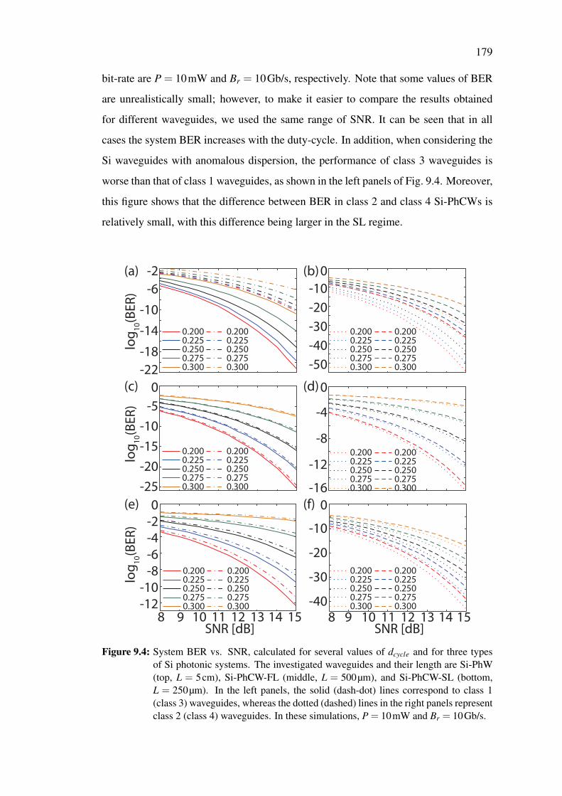
179
bit-rate are P = 10mW and Br = 10Gb/s, respectively. Note that some values of BER
are unrealistically small; however, to make it easier to compare the results obtained
for different waveguides, we used the same range of SNR. It can be seen that in all
cases the system BER increases with the duty-cycle. In addition, when considering the
Si waveguides with anomalous dispersion, the performance of class 3 waveguides is
worse than that of class 1 waveguides, as shown in the left panels of Fig. 9.4. Moreover,
this figure shows that the difference between BER in class 2 and class 4 Si-PhCWs is
relatively small, with this difference being larger in the SL regime.
-22
-18
-14
-10
-6
-2
-50
-40
-30
-20
-10
0
-25
-20
-15
-10
-5
0
-16
-12
-8
-4
0
8 10 11 12 13 14 15SNR [dB]
-12
-10
-8
-6
-4
-2
0
10 11 12 13 14 15SNR [dB]
-40
-30
-20
-10
0
0.2000.2250.2500.2750.300
0.2000.2250.2500.2750.300
0.2000.2250.2500.2750.300
0.2000.2250.2500.2750.300
0.2000.2250.2500.2750.300
0.2000.2250.2500.2750.300
0.2000.2250.2500.2750.300
0.2000.2250.2500.2750.300
0.2000.2250.2500.2750.300
0.2000.2250.2500.2750.300
0.2000.2250.2500.2750.300
0.2000.2250.2500.2750.300
8 99
log
10(B
ER
)lo
g1
0(B
ER
)lo
g1
0(B
ER
)
(a) (b)
(c) (d)
(e) (f)
Figure 9.4: System BER vs. SNR, calculated for several values of dcycle and for three typesof Si photonic systems. The investigated waveguides and their length are Si-PhW(top, L = 5cm), Si-PhCW-FL (middle, L = 500µm), and Si-PhCW-SL (bottom,L = 250µm). In the left panels, the solid (dash-dot) lines correspond to class 1(class 3) waveguides, whereas the dotted (dashed) lines in the right panels representclass 2 (class 4) waveguides. In these simulations, P = 10mW and Br = 10Gb/s.
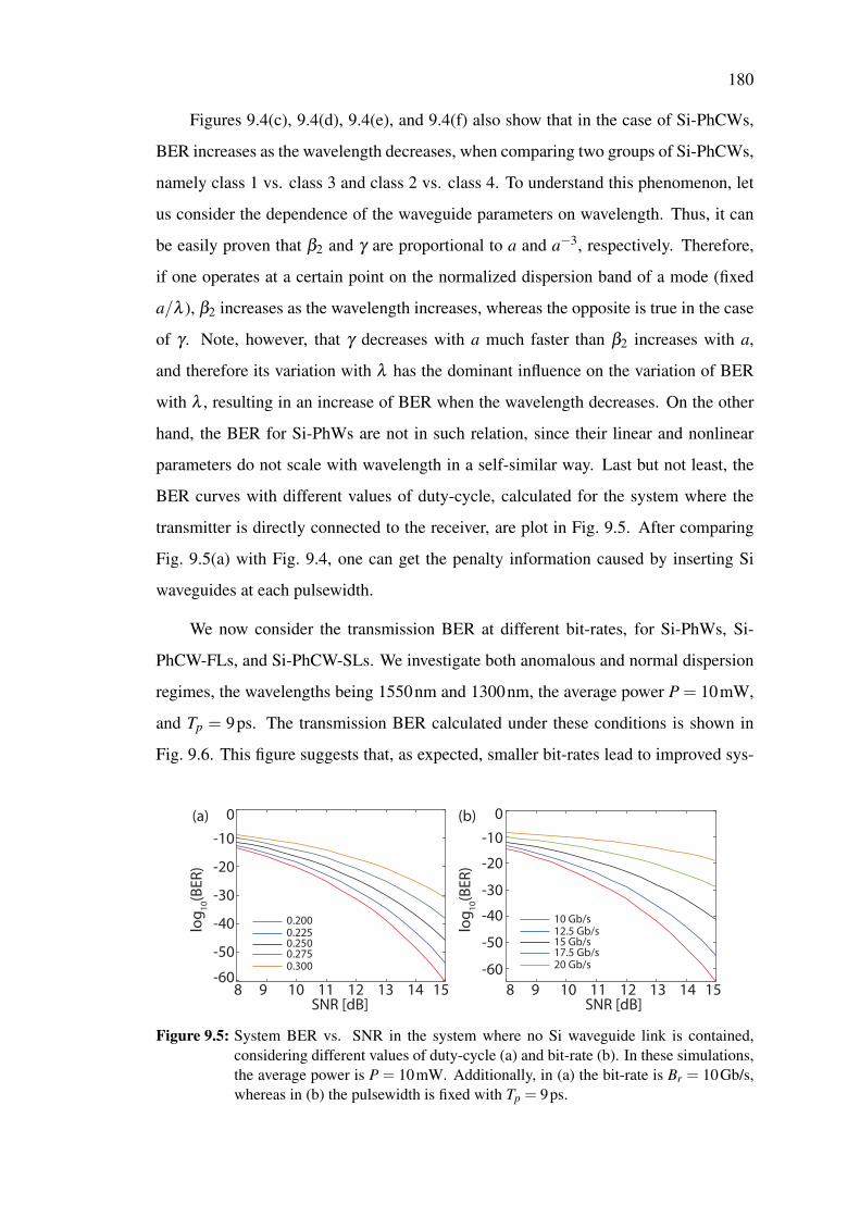
180
Figures 9.4(c), 9.4(d), 9.4(e), and 9.4(f) also show that in the case of Si-PhCWs,
BER increases as the wavelength decreases, when comparing two groups of Si-PhCWs,
namely class 1 vs. class 3 and class 2 vs. class 4. To understand this phenomenon, let
us consider the dependence of the waveguide parameters on wavelength. Thus, it can
be easily proven that β2 and γ are proportional to a and a−3, respectively. Therefore,
if one operates at a certain point on the normalized dispersion band of a mode (fixed
a/λ ), β2 increases as the wavelength increases, whereas the opposite is true in the case
of γ . Note, however, that γ decreases with a much faster than β2 increases with a,
and therefore its variation with λ has the dominant influence on the variation of BER
with λ , resulting in an increase of BER when the wavelength decreases. On the other
hand, the BER for Si-PhWs are not in such relation, since their linear and nonlinear
parameters do not scale with wavelength in a self-similar way. Last but not least, the
BER curves with different values of duty-cycle, calculated for the system where the
transmitter is directly connected to the receiver, are plot in Fig. 9.5. After comparing
Fig. 9.5(a) with Fig. 9.4, one can get the penalty information caused by inserting Si
waveguides at each pulsewidth.
We now consider the transmission BER at different bit-rates, for Si-PhWs, Si-
PhCW-FLs, and Si-PhCW-SLs. We investigate both anomalous and normal dispersion
regimes, the wavelengths being 1550nm and 1300nm, the average power P = 10mW,
and Tp = 9ps. The transmission BER calculated under these conditions is shown in
Fig. 9.6. This figure suggests that, as expected, smaller bit-rates lead to improved sys-
10 11 12 13 14 15SNR [dB]
-60
-50
-40
-30
-20
-10
0
log 10
(BER
)
0.2000.2250.2500.2750.300
98-60
-50
-40
-30
-20
-10
0
log 10
(BER
)
10 11 12 13 14 15SNR [dB]
98
10 Gb/s12.5 Gb/s15 Gb/s17.5 Gb/s20 Gb/s
(a) (b)
Figure 9.5: System BER vs. SNR in the system where no Si waveguide link is contained,considering different values of duty-cycle (a) and bit-rate (b). In these simulations,the average power is P = 10mW. Additionally, in (a) the bit-rate is Br = 10Gb/s,whereas in (b) the pulsewidth is fixed with Tp = 9ps.
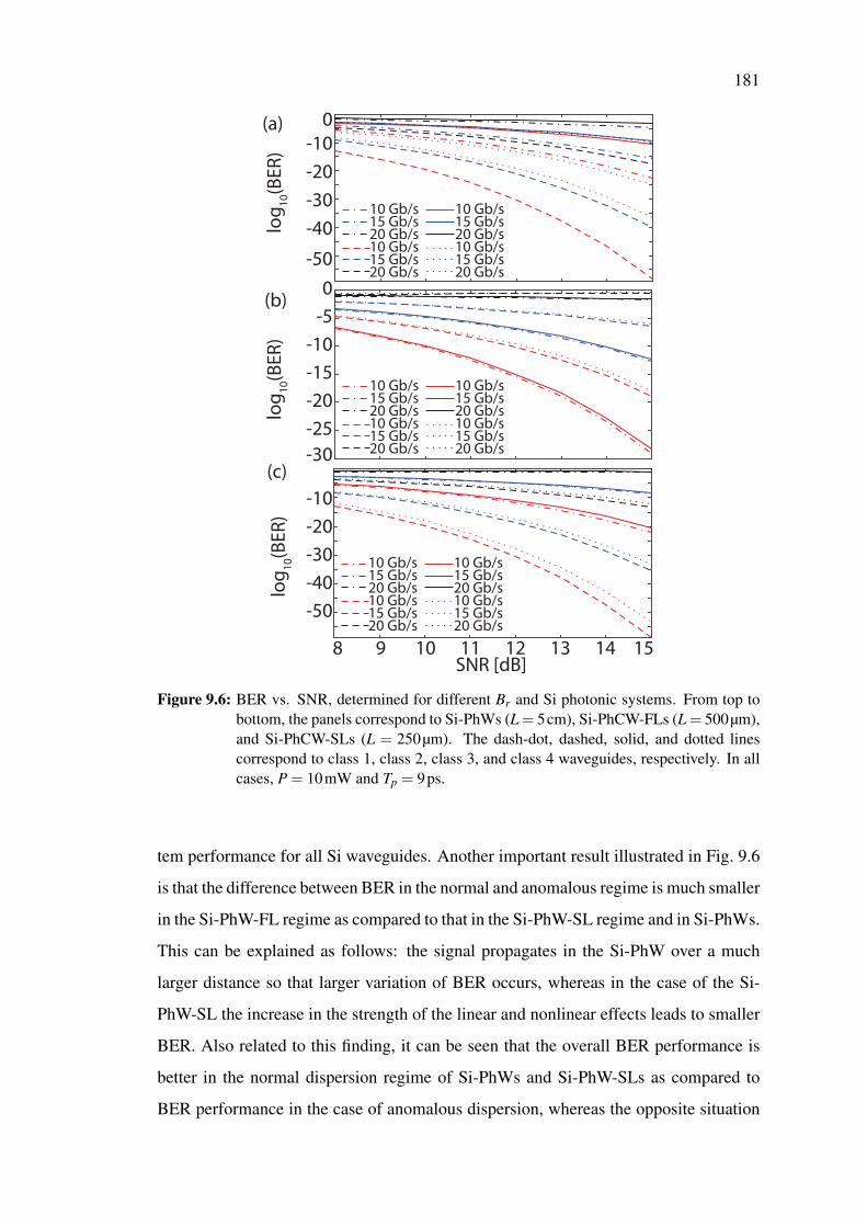
181
10 11 12 13 14 15SNR [dB]
(a)
(b)
(c)
8 9
-50
-40
-30
-20
-10
0
log
10(B
ER
)lo
g1
0(B
ER
)
-50
-40
-30
-20
-10
log
10(B
ER
)
10 Gb/s15 Gb/s20 Gb/s10 Gb/s15 Gb/s20 Gb/s
10 Gb/s15 Gb/s20 Gb/s10 Gb/s15 Gb/s20 Gb/s
-30
-25
-20
-15
-10
-5
0
10 Gb/s15 Gb/s20 Gb/s10 Gb/s15 Gb/s20 Gb/s
10 Gb/s15 Gb/s20 Gb/s10 Gb/s15 Gb/s20 Gb/s
10 Gb/s15 Gb/s20 Gb/s10 Gb/s15 Gb/s20 Gb/s
10 Gb/s15 Gb/s20 Gb/s10 Gb/s15 Gb/s20 Gb/s
Figure 9.6: BER vs. SNR, determined for different Br and Si photonic systems. From top tobottom, the panels correspond to Si-PhWs (L= 5cm), Si-PhCW-FLs (L= 500µm),and Si-PhCW-SLs (L = 250µm). The dash-dot, dashed, solid, and dotted linescorrespond to class 1, class 2, class 3, and class 4 waveguides, respectively. In allcases, P = 10mW and Tp = 9ps.
tem performance for all Si waveguides. Another important result illustrated in Fig. 9.6
is that the difference between BER in the normal and anomalous regime is much smaller
in the Si-PhW-FL regime as compared to that in the Si-PhW-SL regime and in Si-PhWs.
This can be explained as follows: the signal propagates in the Si-PhW over a much
larger distance so that larger variation of BER occurs, whereas in the case of the Si-
PhW-SL the increase in the strength of the linear and nonlinear effects leads to smaller
BER. Also related to this finding, it can be seen that the overall BER performance is
better in the normal dispersion regime of Si-PhWs and Si-PhW-SLs as compared to
BER performance in the case of anomalous dispersion, whereas the opposite situation
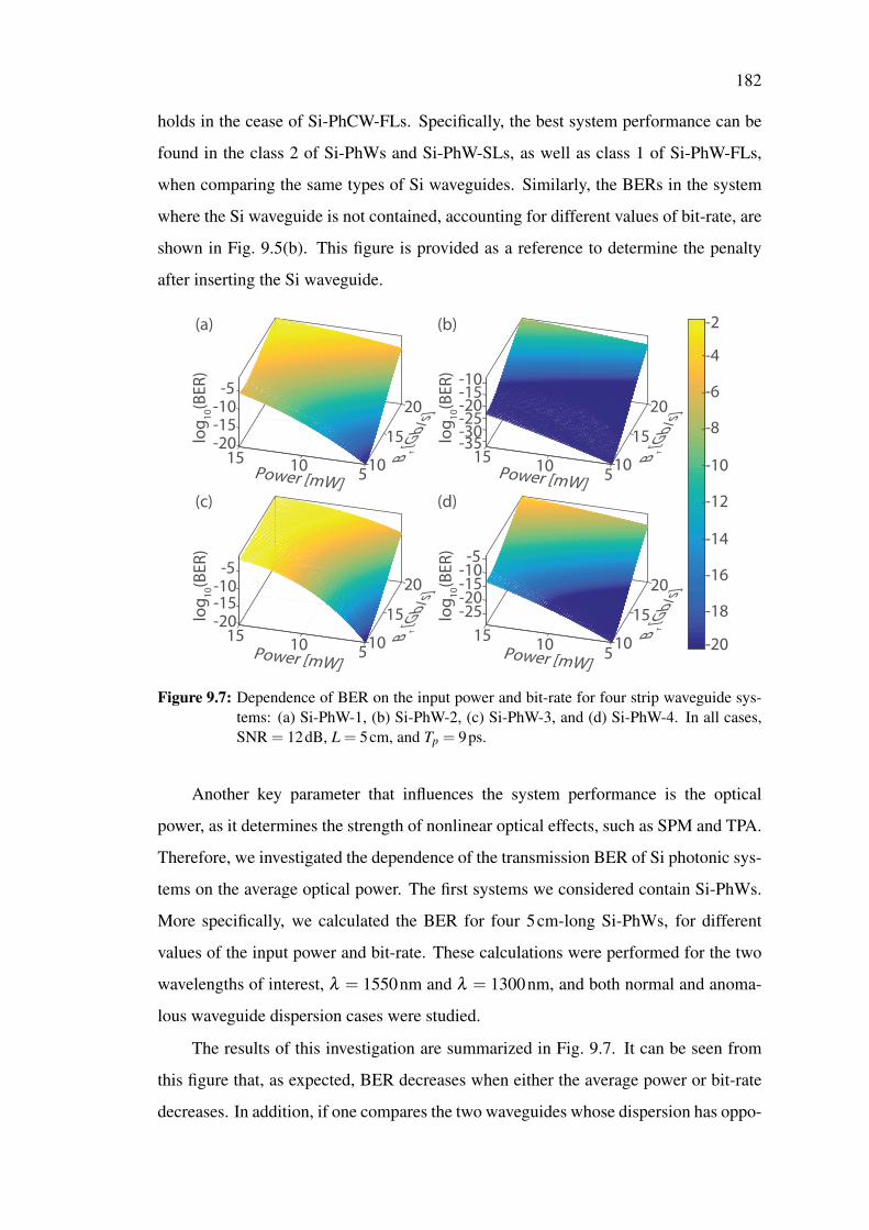
182
holds in the cease of Si-PhCW-FLs. Specifically, the best system performance can be
found in the class 2 of Si-PhWs and Si-PhW-SLs, as well as class 1 of Si-PhW-FLs,
when comparing the same types of Si waveguides. Similarly, the BERs in the system
where the Si waveguide is not contained, accounting for different values of bit-rate, are
shown in Fig. 9.5(b). This figure is provided as a reference to determine the penalty
after inserting the Si waveguide.
20
15-20-15
10
-10-5
-35-30-25-20-15-10
-20
-18
-16
-14
-12
-10
-8
-6
-4
-2
-25-20-15-10
-5
log
10(B
ER
)
15 105Power [mW]
Br [
Gb
/s]
-20-15-10
-5
log
10(B
ER
)
20
15
101510 5Power [mW]
Br [
Gb
/s]
log
10(B
ER
)15
105Power [mW]
20
15
10
Br [
Gb
/s]
log
10(B
ER
)
1510
5Power [mW]
20
15
10B
r [G
b/s
]
(a) (b)
(c) (d)
Figure 9.7: Dependence of BER on the input power and bit-rate for four strip waveguide sys-tems: (a) Si-PhW-1, (b) Si-PhW-2, (c) Si-PhW-3, and (d) Si-PhW-4. In all cases,SNR = 12dB, L = 5cm, and Tp = 9ps.
Another key parameter that influences the system performance is the optical
power, as it determines the strength of nonlinear optical effects, such as SPM and TPA.
Therefore, we investigated the dependence of the transmission BER of Si photonic sys-
tems on the average optical power. The first systems we considered contain Si-PhWs.
More specifically, we calculated the BER for four 5cm-long Si-PhWs, for different
values of the input power and bit-rate. These calculations were performed for the two
wavelengths of interest, λ = 1550nm and λ = 1300nm, and both normal and anoma-
lous waveguide dispersion cases were studied.
The results of this investigation are summarized in Fig. 9.7. It can be seen from
this figure that, as expected, BER decreases when either the average power or bit-rate
decreases. In addition, if one compares the two waveguides whose dispersion has oppo-
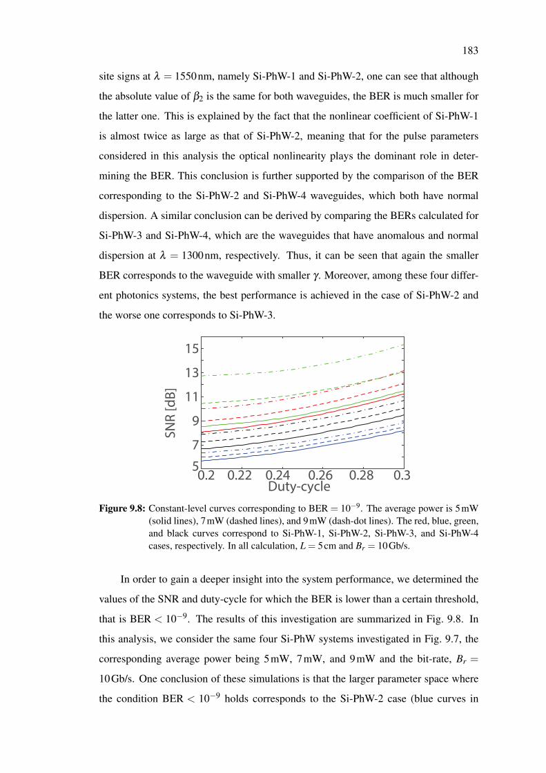
183
site signs at λ = 1550nm, namely Si-PhW-1 and Si-PhW-2, one can see that although
the absolute value of β2 is the same for both waveguides, the BER is much smaller for
the latter one. This is explained by the fact that the nonlinear coefficient of Si-PhW-1
is almost twice as large as that of Si-PhW-2, meaning that for the pulse parameters
considered in this analysis the optical nonlinearity plays the dominant role in deter-
mining the BER. This conclusion is further supported by the comparison of the BER
corresponding to the Si-PhW-2 and Si-PhW-4 waveguides, which both have normal
dispersion. A similar conclusion can be derived by comparing the BERs calculated for
Si-PhW-3 and Si-PhW-4, which are the waveguides that have anomalous and normal
dispersion at λ = 1300nm, respectively. Thus, it can be seen that again the smaller
BER corresponds to the waveguide with smaller γ . Moreover, among these four differ-
ent photonics systems, the best performance is achieved in the case of Si-PhW-2 and
the worse one corresponds to Si-PhW-3.
SNR
[dB]
0.2 0.22 0.24 0.26 0.28 0.3Duty-cycle
5
7
9
11
13
15
Figure 9.8: Constant-level curves corresponding to BER = 10−9. The average power is 5mW(solid lines), 7mW (dashed lines), and 9mW (dash-dot lines). The red, blue, green,and black curves correspond to Si-PhW-1, Si-PhW-2, Si-PhW-3, and Si-PhW-4cases, respectively. In all calculation, L = 5cm and Br = 10Gb/s.
In order to gain a deeper insight into the system performance, we determined the
values of the SNR and duty-cycle for which the BER is lower than a certain threshold,
that is BER < 10−9. The results of this investigation are summarized in Fig. 9.8. In
this analysis, we consider the same four Si-PhW systems investigated in Fig. 9.7, the
corresponding average power being 5mW, 7mW, and 9mW and the bit-rate, Br =
10Gb/s. One conclusion of these simulations is that the larger parameter space where
the condition BER < 10−9 holds corresponds to the Si-PhW-2 case (blue curves in
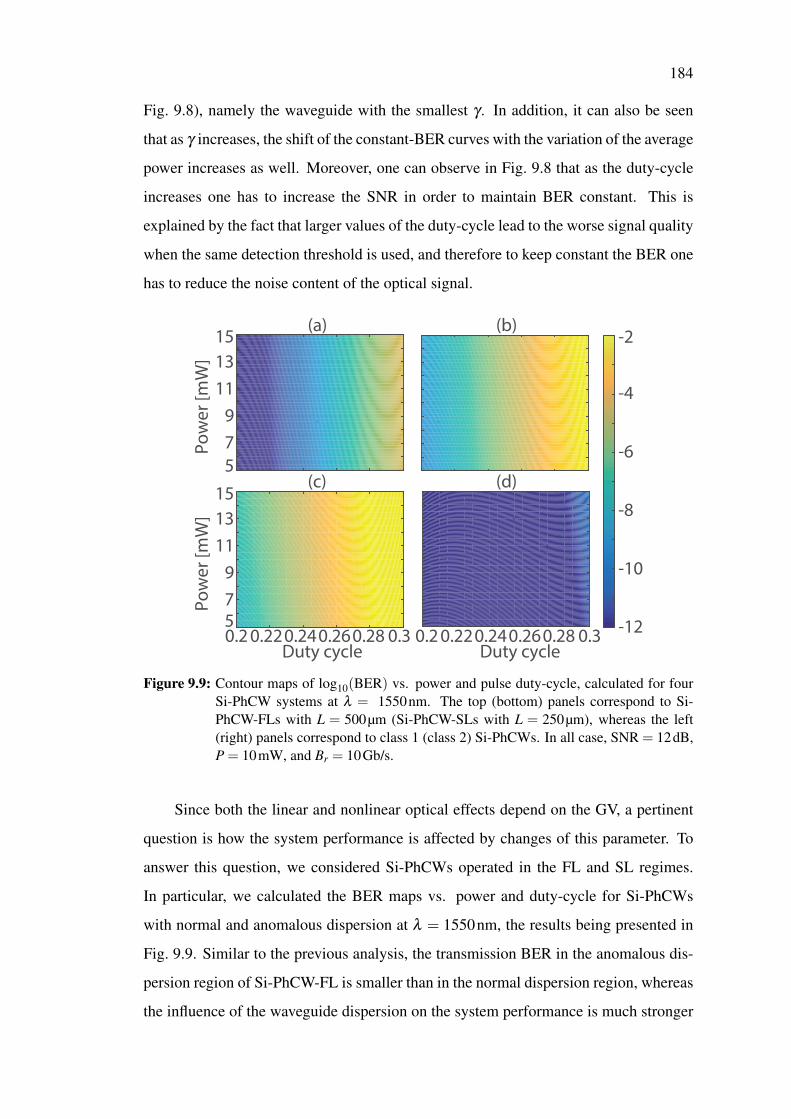
184
Fig. 9.8), namely the waveguide with the smallest γ . In addition, it can also be seen
that as γ increases, the shift of the constant-BER curves with the variation of the average
power increases as well. Moreover, one can observe in Fig. 9.8 that as the duty-cycle
increases one has to increase the SNR in order to maintain BER constant. This is
explained by the fact that larger values of the duty-cycle lead to the worse signal quality
when the same detection threshold is used, and therefore to keep constant the BER one
has to reduce the noise content of the optical signal.
5
7
9
11
13
15
Po
we
r [m
W]
-12
-10
-8
-6
-4
-2
0.2 0.220.240.260.28 0.3Duty cycle
(a)
57
9
11
13
15
Po
we
r [m
W]
(c)
0.2 0.220.240.260.28 0.3Duty cycle
(b)
(d)
Figure 9.9: Contour maps of log10(BER) vs. power and pulse duty-cycle, calculated for fourSi-PhCW systems at λ = 1550nm. The top (bottom) panels correspond to Si-PhCW-FLs with L = 500µm (Si-PhCW-SLs with L = 250µm), whereas the left(right) panels correspond to class 1 (class 2) Si-PhCWs. In all case, SNR = 12dB,P = 10mW, and Br = 10Gb/s.
Since both the linear and nonlinear optical effects depend on the GV, a pertinent
question is how the system performance is affected by changes of this parameter. To
answer this question, we considered Si-PhCWs operated in the FL and SL regimes.
In particular, we calculated the BER maps vs. power and duty-cycle for Si-PhCWs
with normal and anomalous dispersion at λ = 1550nm, the results being presented in
Fig. 9.9. Similar to the previous analysis, the transmission BER in the anomalous dis-
persion region of Si-PhCW-FL is smaller than in the normal dispersion region, whereas
the influence of the waveguide dispersion on the system performance is much stronger
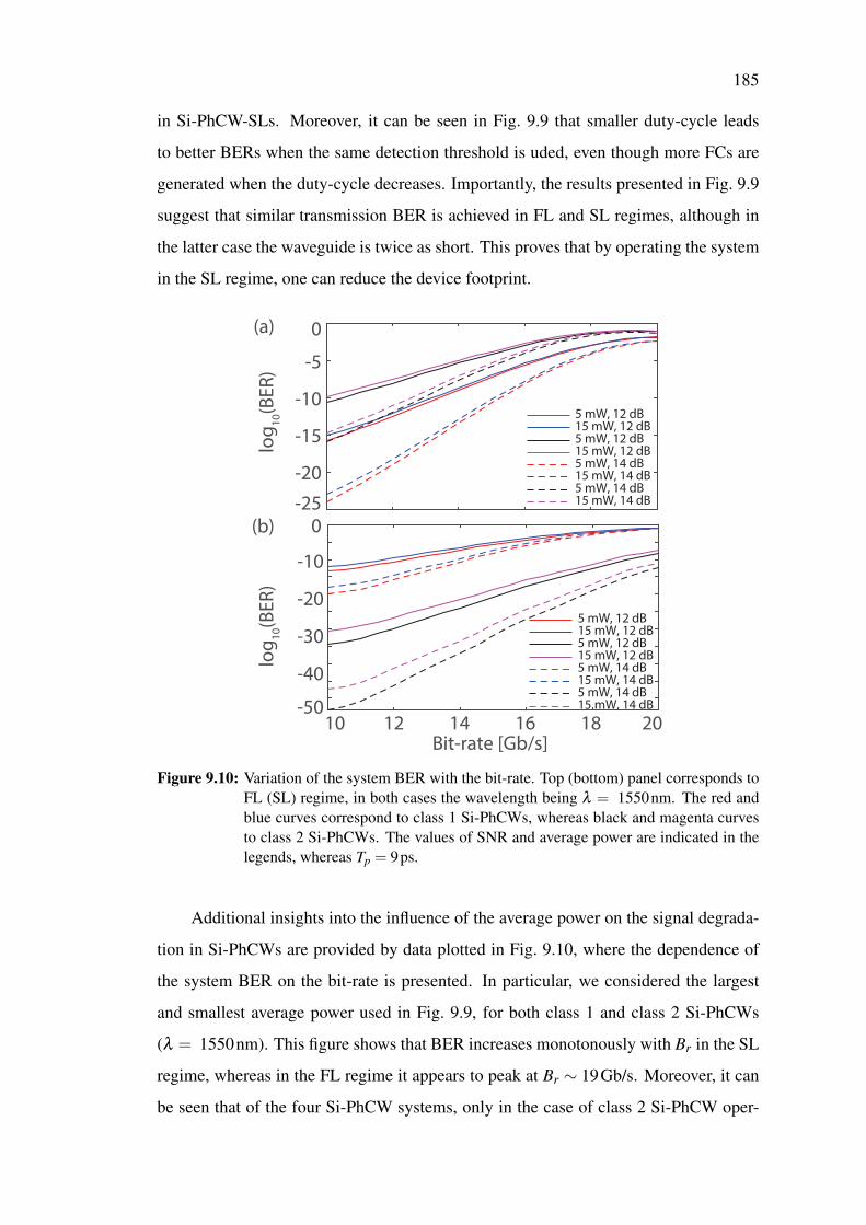
185
in Si-PhCW-SLs. Moreover, it can be seen in Fig. 9.9 that smaller duty-cycle leads
to better BERs when the same detection threshold is uded, even though more FCs are
generated when the duty-cycle decreases. Importantly, the results presented in Fig. 9.9
suggest that similar transmission BER is achieved in FL and SL regimes, although in
the latter case the waveguide is twice as short. This proves that by operating the system
in the SL regime, one can reduce the device footprint.
-25
-20
-15
-10
-5
0
log
10(B
ER
)
10 12 14 16 18 20Bit-rate [Gb/s]
-50
-40
-30
-20
-10
0
(a)
(b)
log
10(B
ER
)
5 mW, 12 dB15 mW, 12 dB5 mW, 12 dB15 mW, 12 dB5 mW, 14 dB15 mW, 14 dB5 mW, 14 dB15 mW, 14 dB
5 mW, 12 dB15 mW, 12 dB5 mW, 12 dB15 mW, 12 dB5 mW, 14 dB15 mW, 14 dB5 mW, 14 dB15 mW, 14 dB
Figure 9.10: Variation of the system BER with the bit-rate. Top (bottom) panel corresponds toFL (SL) regime, in both cases the wavelength being λ = 1550nm. The red andblue curves correspond to class 1 Si-PhCWs, whereas black and magenta curvesto class 2 Si-PhCWs. The values of SNR and average power are indicated in thelegends, whereas Tp = 9ps.
Additional insights into the influence of the average power on the signal degrada-
tion in Si-PhCWs are provided by data plotted in Fig. 9.10, where the dependence of
the system BER on the bit-rate is presented. In particular, we considered the largest
and smallest average power used in Fig. 9.9, for both class 1 and class 2 Si-PhCWs
(λ = 1550nm). This figure shows that BER increases monotonously with Br in the SL
regime, whereas in the FL regime it appears to peak at Br ∼ 19Gb/s. Moreover, it can
be seen that of the four Si-PhCW systems, only in the case of class 2 Si-PhCW oper-
186
ated in the SL regime is the system BER below the threshold of 10−9, for all values of
Br in the range of 10 Gb/s to 20 Gb/s. Further validating our previous conclusions, the
results presented in Fig. 9.10 also demonstrate a stronger dependence of BER on the
average power in the SL regime as compared to the FL one. Finally, in agreement with
previous results, it can be seen that the 2× shorter Si-PhCW-SL provides better system
performance than the Si-PhCW-FL, meaning that there is large potential for designing
extremely compact Si optical interconnects that operate at high bit-rate.
9.5 ConclusionIn conclusion, we have performed an extensive and in-depth study of transmission bit-
error ratio in silicon photonic systems utilizing return-to-zero optical signals consisting
of trains of Gaussian pulses. The photonic systems are composed of silicon photonic
waveguides and direct-detection receivers. A rigorous theoretical model is developed
and applied to characterize all the key optical effects during pulse propagation in silicon
waveguides, and the Fourier-series Karhunen-Loeve expansion method in conjunction
with a perturbation theory are employed to evaluate the system bit-error ratio after
direct-detection. In order to fully assess the influence of the waveguide parameters on
the system performance, we considered in this work both strip silicon photonic wires
and silicon photonic crystal waveguides, with each waveguide possessing normal and
anomalous dispersion. In addition, the silicon photonic crystal waveguides studied in
this work possessed slow- and fast-light dispersion regimes, so that we could inves-
tigate the influence of the group-velocity on the bit-error ratio. We also explored the
relationships between the bit-error ratio and other key system parameters, including the
pulse wavelength and temporal width, power, and bit-rate.
Our computational results suggest that suitable and commensurate system bit-error
ratios can be achieved in silicon photonic wires and photonic crystal waveguides, but
in the latter case the waveguide length is about 100× shorter when operating in the
fast-light regime and about 200× shorter when the optical signal propagates in the
slow-light regime. Importantly for future studies of the performance of silicon-based
photonic systems, the mathematical formalism introduced in this paper can also be
applied to other optical waveguides and more sophisticated photonic integrated circuits,
thus providing a basis for future technological advancements in silicon-based on-chip

187
and chip-to-chip optical networks.
188
Bibliography[1] X. Chen, N. C. Panoiu, and R. M. Osgood, “Theory of Raman-mediated pulsed
amplification in silicon-wire waveguides,” IEEE J. Quantum Electron. 42, 160-
170 (2006).
[2] J. You and N. C. Panoiu, “Calculation of Bit Error Rates in Optical Systems with
Silicon Photonic Wires,” IEEE J. Quantum Electron. 51, 8400108 (2015).
[3] N. C. Panoiu, J. F. McMillan, and C. W. Wong, “Theoretical analysis of pulse dy-
namics in silicon photonic crystal wire waveguides,” IEEE J. Sel. Top. Quantum
Electron. 16, 257-266 (2010).
[4] S. Lavdas and N. C. Panoiu, “Theory of Pulsed Four-Wave-Mixing in One-
dimensional Silicon Photonic Crystal Slab Waveguides,” Phys. Rev. B 93, 115435
(2016).
[5] R. Holzlohner, C. R. Menyuk, W. L. Kath, and V. S. Grigoryan, “Efficient and
Accurate Computation of Eye Diagrams and Bit-Error Rates in a Single-Channel
CRZ System,” IEEE Photon. Technol. Lett. 14, 1079-1081, (2002).
Chapter 10
Conclusions and Future work
Silicon photonic waveguides have attracted extensive research efforts during the last
two decades, due to their abilities of facilitating ultrafast optical interconnects and
ultra-dense passive and active photonic devices. The outstanding properties of silicon
photonic waveguides, including the large transparency window, subwavelength cross-
sections, strong dispersion and nonlinearity, as well as the good compatibility with
CMOS circuitries, provide great opportunities to the next-generation information net-
works. Even though all the essential parts of silicon photonics have been investigated
nowadays, including the scientific exploration, design, fabless, foundries, devices and
systems, the whole silicon photonics ecosystem is under research and development
stage. Therefore, it is extremely important to study the underlying physics of silicon
photonic waveguides, by means of the theoretical and computational approaches. This
would not only allow the engineering of more complicated silicon photonic systems,
but also enable the implementation of the most up-to-date photonic materials and de-
vices in practice.
This dissertation serves as a promising solution to settle the realistic issues raised
above. The emphasis of this work is put on the investigation and demonstration of
the nonlinear signal processing in the photonic systems containing nanoscale silicon
waveguides. More precisely, two sets of mathematical models have been proposed in
this dissertation, namely, the optical signal propagation models for silicon waveguides
and the accurate BER calculation models. In particular, regarding the first set of theo-
retical models, a linearized version of the full propagation models is derived, which is
specified for the photonic systems utilizing continuous-wave (CW) signals. These two
propagation models accurately characterize all the linear and nonlinear optical effects
190
within silicon photonic waveguides. Furthermore, the second set of mathematical mod-
els are based on the Karhunen-Loeve series expansion methods, which can be applied
to calculate the system BER in an accurate and efficient way. Therefore, the theoretical
models and numerical algorithms introduced in this dissertation can be very useful to
design high-performance photonic devices and integrated photonic circuitries, as well
as provide a complete induction of the significant optical phenomena within the silicon
photonic waveguides.
The following sections will present my original contributions to the field of silicon
photonics and the future prospectives to the area of photonics.
10.1 ContributionsThe main contributions of this dissertation in the development of silicon photonics can
be divided into two aspects: firstly, this work helps provide the rigorous theoretical and
numerical models for the investigation of nonlinear signal propagation in silicon pho-
tonic waveguides; secondly, the accurate BER evaluation approaches are recommended
to deal with the nonlinear interaction between the signal and the noise in particular.
Importantly, the complete system analysis model has been numerically implemented
as a Matlab tool. Furthermore, the accurate analysis towards silicon photonic systems,
which is obtained by using this Matlab tool, has shown that it is of great importance to
employ the theoretical and computational approaches in the design of silicon intercon-
nects and optical devices, and the corroboration and optimization of the experimental
work.
To be more specific, an accurate computational model is developed to simulate the
the optical signal propagation in two specially designed silicon waveguides, namely the
single-mode strip silicon photonic waveguides and the photonic crystal silicon waveg-
uides. Both cases of single- and multi-wavelength input signals have been taken into
account, thus two sets of the full propagation models are yielded. Furthermore, the
linearized models are extracted from the full propagation approaches for the CW input
signals, by means of discarding all quadratic and higher-order noise terms in the orig-
inal formulations. Notably, these two types of propagation models are mathematically
and numerically proved that they can accurately incorporate all important optical ef-
fects, including the waveguide loss, GVD, SPM, XPM, FCA and FCD, as well as the
191
mutual interaction between free carriers and the optical field. Moreover, two groups of
comprehensive investigations are carried out: one is the detailed comparison between
the normal and anomalous dispersion regions of silicon photonic waveguides, with the
other being the comparison between the fast-light and slow-light spectral regimes. In
this process, the noise dynamics is studied in combination with different types of signal
modulation formats. Last but not least, the numerical implementation of the full and
linearized algorithms for optical signal propagation is also provided in this disserta-
tion, which allows for extensively investigation regarding nonlinear optical response in
silicon photonic waveguides.
Furthermore, accurate and efficient theoretical models are constructed for BER
calculation in this dissertation. Specifically, three BER calculation approaches based on
the time-domain, frequency-domain and Fourier-series Karhunen-Loeve series expan-
sion, are presented, in order to fully capture the waveguide nonlinearity in silicon pho-
tonic systems. Moreover, the discussion with regard to the applications and advantages
of these expansion methods is also presented. Particularly, the time- and frequency-
domain Karhunen-Loeve series expansion methods are selected for the evaluation of
BER with regard to CW optical signals, whereas the Fourier-series Karhunen-Loeve
series expansion method is employed for the case of optical pulsed signals. In addi-
tion, rigorous computational procedures are included for the implementation of these
Karhunen-Loeve expansion methods in the system performance evaluation, consider-
ing both single- and multi-channel silicon photonic systems.
Apart from the major contributions of establishing the performance evaluation en-
gine for silicon photonic systems, literature reviews in the aspect of silicon photonics,
optical interconnects, silicon waveguides and BER calculation methods, are also pro-
vided in this dissertation. These concise summaries can help one better understand the
background, connections between each of those fields, and the importance of this work.
Equipped with this theoretical and computational tools, the comprehensive analy-
sis are performed for the single-channel and multi-channel photonic systems. Several
valuable and remarkable findings can be drawn from this PhD project, which definitely
contributes to the development of silicon photonics:
• In terms of the single-channel strip silicon photonic systems with the OOK CW
signals, the geometry of silicon waveguides and the power of optical signal play
192
an important role when determining the system BER. In addition, the BER de-
pendence on these two factors becomes more transparent in the anomalous dis-
persion region of silicon waveguide, where the nonlinearity is much larger than
that of normal dispersion.
• The analysis of the single-channel silicon photonic crystal systems reveals that
although slow-light effects can enhance the waveguide nonlinearity, they also
cause a significant degradation of the transmission BER.
• With regard to the higher-order PSK modulation formats, the studies of the
single-channel strip and photonic crystal systems indicate that the optical power,
type of PSK modulation, waveguide length, and group-velocity are key factors
characterizing the system BER, their influence on BER being more significant
in a photonic system with larger nonlinearity. In particular, due to the reduced
Euclidean spacing between points in the constellation of PSK signals, the higher-
order PSK modulated signals would induce larger system BERs, and thus the
balance between the high information capacity (orders of PSK modulation) and
good signal quality (BER) must be reached.
• The rigorous mathematical algorithms are developed for the N-channel signal
co-propagation and the receiver detection. The relevant simulations show that
the BER affecting factors in the multi-channel system performance include the
dispersion regimes, group-velocity, the waveguide length, the channel number
and the signal power.
• The case of single-channel silicon photonic systems utilizing arbitrary Gaussian
pulsed signals is also investigated in this dissertation. The simulation results sug-
gest that a good system performance is achieved in centimeter-long Si-PhWs,
and a similar case of BER is also realized in Si-PhCWs but with their length
100× and 200× shorter when operating in the fast- and slow-light regimes, re-
spectively. However, the pulse width of Gaussian-pulse signals is the dominant
parameter to influence the BER in Si-PhWs, while for Si-PhCWs the main factor
turns out to be the waveguide properties via the pulse group-velocity.
• The complete system evaluation model is implemented in Matlab. This Matlab
193
engine has the scan function, which can be run in serial or in parallel. It is
beneficial to use the parallel run, considering the computational time.
10.2 Future ProspectsSilicon photonics are promising to settle the bottlenecks of ultra-broad bandwidth and
highly integrated supercomputers and data centers, thus substantial research efforts
have been and will be contributed to this field. As mentioned before, a full supply
of silicon photonics is under the stage of research and development, requiring loads
of improvements to enable the commercialization of silicon photonic products in the
near future. The theoretical and computational models demonstrated in this disserta-
tion definitely provide a valuable and efficient tool for the design of chip-scale optical
interconnects. Apart from the goals presented earlier, the signal propagation models
and BER calculation approaches can be widely applied in abundant aspects, which I
will give a detailed explanation in the next few paragraphs.
Firstly, it would be very beneficial to include more complicated nonlinear effects
like FWM and Raman scattering in the signal propagation models. An interesting ex-
ample is to consider the Raman effect in a two-channel silicon photonic system, where
one channel contains a CW signal and the white noise, while the other channel only
consisting of the white noise. The first channel will behaves as the pump to yield the
signal generation in the other channel. Moreover, their nonlinear interaction during
transmission may bring out some new phenomena. Therefore, a signal propagation
model that owns the flexibility to engineer the optical properties of silicon waveguides,
will absolutely offer more possibilities to the functionalities of photonic devices.
Secondly, from practical point of view, all types of system noise can be taken
into account in the BER calculation that based on the Karhunen-Loeve series expan-
sion, including the laser phase noise, the spontaneous emission noise, receiver thermal
noise and signal shot noise. In general, this all-inclusive evaluation is usually carried
out by using the Monte-Carlo method, with the accuracy guaranteed by the computa-
tional time. But when compared with the newly-proposed BER calculation method, the
Monte-Carlo method is lack of the advantage in the computational cost.
Furthermore, the theoretical formalism introduced in this dissertation can also
be applied to other types of waveguides or more complex devices practical interest.
194
For example, our theoretical approach can applied to tapered, slot, and other types of
waveguides by simply using the corresponding linear and nonlinear waveguide optical
coefficients. Moreover, after properly modifying the system of equations governing
the optical field dynamics in silicon waveguides, a similar theoretical formalism can be
employed study the transmission BER of photonic systems containing, e.g., splitters,
ring modulators coupled to a waveguide, and multi-mode waveguides. Equally impor-
tant, the generality the theoretical methods used in this study makes it easy to adapt
them to tackle much more advanced signal modulation formats and detection schemes
than those considered in this work.
Last but not least, a more sophisticated modeling platform can be built based on
the evaluation engine provided in this dissertation. To be more specific, the current
engine will serves as the physical layer, with the other two layers to be the network and
the application. Even though large amount of theoretical and numerical investigations
are required to carry out, such a integrated simulation platform can definitely contribute
to the revolution of the next-generation information network.
Appendix A
Gauss-Hermite Algorithm
The Gauss-Hermite algorithm is applied in this dissertation to handle the convolution
of Eqs. (3.9) and (3.10). A general form of Gauss-Hermite quadrature is illustrated
below to approximate such integral:
∫∞
−∞
e(−τ2)f(τ)dτ ≈M
∑j=1
ω jf(τ j), (A.1)
where τ j and ω j are the abscissas and associated weights, respectively. By operating
the Gauss-Hermite technique to Eqs. (3.9) and (3.10) and choosing the same time step
of τ j, the discretized formulas are yield:
M
∑j=1
ω jhe(τ j)ρki (tm− τ j)φ
kα(τ j) = µ
kαφ
kα(tm), (A.2a)
M
∑j=1
ω jhe(τ j)ρkq(tm− τ j)ψ
kα(τ j) = ν
kαψ
kα(tm), (A.2b)
M
∑j=1
ω jhe(tm)he(τ j)ρkiq(τ j− tm)ψk
β(τ j) = σ
kαβ
φkα(tm), (A.2c)
where m, j = 1, ...,M. Then, solving Eqs. (3.9) and (3.10) is transferred to find the
eigenvalues and eigenfunctions, based on the relations below:
Ci ·F1 = Λkµ ·F1, (A.3a)
Cq ·F2 = Λkν ·F2, (A.3b)
Ciq ·F1 = Σk ·F1, (A.3c)

196
with the explicit expressions of the related matrixes listed below:
(F1) jα = φkα(tm), F2
jα = ψkα(tm), (A.4a)
(Ci/q)m j = ω jhe(τ j)ρki/q(tm− τ j),
(Ciq)m j = ω jhe(tm)he(τ j)ρkiq(τ j− tm), (A.4b)
(Λkµ)m j = µ
kαδm j, (Λk
ν)m j = νkαδm j, (Σk)m j = σ
kαβ|α=m,β= j. (A.4c)
To this end, the mathematical solutions for Eqs. (3.9) and (3.10) are ready to be de-
rived.

Appendix B
Fifth-order Runge-Kutta Algorithm
The Runge-Kutta method is usually applied in the ODEs, in order to extract the semi-
analytical solutions. Its mathematical process is to first collect data from a few Euler-
steps, with each step accounting for one calculation of the right-hand side of the ODE,
and then utilize the data to approach a desired Taylor series expansion. Here, the nu-
merical implementation of the fifth-order Runge-Kutta algorithm in Matlab will be
presented. In particular, a self-constructed Matlab code based on the fifth-order Runge-
Kutta algorithm is applied, in order to calculate the FCs density for the full propagation
model, whereas the Matlab built-in function ode45 is utilized for the evaluation of the
ODEs in the linearized model. Moreover, these two approaches share exactly the same
mathematical formulae.
Table B.1: Cash-Karp paramters for embedded Runge-Kutta method.
j a j b jm c j
1 0 0 0 0 0 0 37378
2 15
15 0 0 0 0 0
3 310
340
940 0 0 0 250
621
4 35
310 − 9
1065 0 0 125
594
5 1 −1154 −5
2 −7027
3527 0 0
6 78
163155296
175512
57513824
44275110592 − 253
4096512
1771
m = 1 2 3 4 5
The start point is to select the suitable points tn for Eq. (2.39), where both condi-
tions of continuity and differentiability are satisfied, in order to approximate y(tn) with
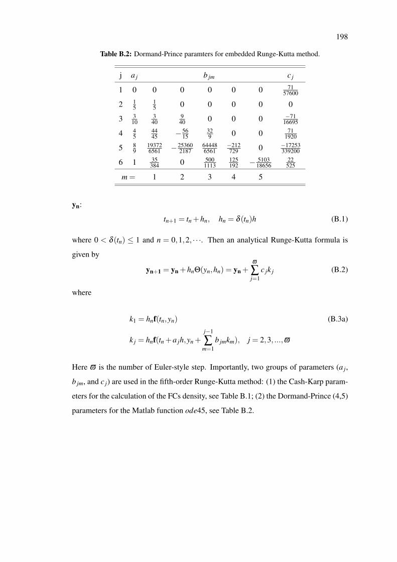
198
Table B.2: Dormand-Prince paramters for embedded Runge-Kutta method.
j a j b jm c j
1 0 0 0 0 0 0 7157600
2 15
15 0 0 0 0 0
3 310
340
940 0 0 0 −71
16695
4 45
4445 −56
15329 0 0 71
1920
5 89
193726561 −25360
2187644486561
−212729 0 −17253
339200
6 1 35384 0 500
1113125192 − 5103
1865622525
m = 1 2 3 4 5
yn:
tn+1 = tn +hn, hn = δ (tn)h (B.1)
where 0 < δ (tn) ≤ 1 and n = 0,1,2, · · ·. Then an analytical Runge-Kutta formula is
given by
yn+1 = yn +hnΘ(yn,hn) = yn +ϖ
∑j=1
c jk j (B.2)
where
k1 = hnf(tn,yn) (B.3a)
k j = hnf(tn +a jh,yn +j−1
∑m=1
b jmkm), j = 2,3, ...,ϖ
Here ϖ is the number of Euler-style step. Importantly, two groups of parameters (a j,
b jm, and c j) are used in the fifth-order Runge-Kutta method: (1) the Cash-Karp param-
eters for the calculation of the FCs density, see Table B.1; (2) the Dormand-Prince (4,5)
parameters for the Matlab function ode45, see Table B.2.

Appendix C
Golden Section Algorithm
Golden Section Algorithm is a numerical scheme that often used in search of the max-
imum or minimum value of a function over an interval. Its mathematical process is
to continuously reduce the interval until the extremum point of the function is located.
To simply mathematical discussion, I will take the minimization problem for example,
which also coincide with the issue of saddle points raised in Sec. 3.5.
To start with, a function f(x) with the variable x is defined. Specifically, f(x) is
assumed to be continuous over the integral of [a,b] and have only one minimum in this
range. Aiming at using a constant fraction to narrow the search range and reduce the
number of function evaluation as much as possible, the main steps of Golden Section
Algorithm are demonstrated as follows. Notably the constant fraction is referred as
golden ratio, with the value of wgold = (3−√
5)/2.
1. Select two specific points x1 and x2 inside the interval [a,b]. These two points
are defined as x1 = a+d and x2 = b−d, where d = wgold(b−a).
2. Calculate the functions of f(x1) and f(x2).
3. Make a decision based on the relative value between f(x1) and f(x2).
(a) If f(x1)> f(x2), the minimum of f(x) must be located at the right of x1. The
new value is given to a according to such relation of a = x1, while the value
of b is kept unchanged.
(b) If f(x1)< f(x2), the minimum of f(x) must be located at the left of x2. The
new value is given to b according to such relation of b = x2, while the value
of a remains the same.
200
4. Determine if the minimum of f(x) is found under the condition of b− a < σ ,
where σ is the tolerance of this algorithm. If so, the minimum occurs at (a+b)/2
and stop the iteration. Otherwise repeat the procedure from Step 1.
In this dissertation, the tolerance of the Golden Section Algorithm is set to
σ = 10−8. With regard to the process of deriving the saddle points, as mentioned
in Sec. 3.5, it can be classified into two categories. In particular, the first procedure
relates to the time-domain KLSE method, while the second one corresponds to the
frequency-domain and Fourier-series KLSE approaches, with the difference being the
function f(x). To be more specific, referring to Eq. (3.39) (time-domain KLSE), the
saddle point s−o for signal “0” is extracted, by using the Golden Section Algorithm to
find the minimum of exp[Φyk(s)] over the interval of [−1/(max |2δk,−α |),0]. And the
same numerical routine is applied on exp[Φyk(s)] in the interval [0,+∞], in order to
find the second saddle point s+o for signal “1”. However, the search for saddle points
in the frequency-domain and Fourier-series KLSE is based on Eq. (3.42). Thus, the
calculation of the saddle point s+o for signal “0” is carried out by using the algorithm
proposed in this section over the interval of [0,1/(max |2λ+n |)] and [0,1/(max |2ε+p |)],
which correspond to the frequency-domain and Fourier-series KLSE approaches, re-
spectively. In the meanwhile, the value of s−o for signal “1” is extracted by using the
same technique but in the range of [−∞,0], validated in both frequency-domain and
Fourier-series KLSE methods. To this end, the saddle points used in all the KLSE
methods have been settled.
Related Documents