CA330 RTD Calibrator: High-speed Response and High-resolution Resistance Simulator Yokogawa Technical Report English Edition Vol.59 No.2 (2016) CA330 RTD Calibrator: High-speed Response and High-resolution Resistance Simulator Kouki Shouji *1 Yokogawa Meters & Instruments Corporation has developed the CA330 handheld process calibrator, a resistance temperature detector (RTD) model. We thoroughly reviewed the design of the ohms source function which has been a long-standing problem. In particular, high resolution and high-speed response were achieved by using a new technology of the improved feedback type PWM method, thus successfully raising the carrier frequency without degrading the PWM resolution. As a result, we changed the demodulation processing of the multiplying digital-to-analog converter (DAC) with pulse width modulation (PWM) from the conventional section integration method to a simple low-pass filter method, increasing the processing speed. As a result, the CA330 has achieved a response of less than 5 msec with the setting resolution of 10 mW. This paper introduces the redesigned ohms source function and improved feedback-type PWM. INTRODUCTION M any instrumentation devices are installed in various processes in automated factories to convert physical quantities such as temperature, pressure, and flow rate into transmission signals in the form of voltage or current. To inspect and calibrate such devices quickly, handheld process calibrators are required. Yokogawa released the CA12E handheld temperature calibrator ten years ago. Since then, the functions of instrumentation devices have advanced remarkably but the performance of existing models as a calibrator has become insufficient. In particular, measuring instruments that use a platinum resistance temperature detector (RTD) or other high- accuracy RTD as a temperature sensor require a calibrator to simulate resistance with high accuracy and high resolution over a wide range of excitation current. For simulating Pt100 (typical platinum RTD) at a resolution of 0.1°C, the resolution is equivalent to 30 mW on the resistance scale. Therefore, the accuracy of voltage generation is required to be within 3 µV at the excitation current of 100 µA. In addition, recent recorders with multi-channel, fast scanning require a sufficiently high- speed response to follow the channel switching time. To respond to such requirements, Yokogawa Meters & Instruments has newly developed the CA330 with even better performance than existing models. Figure 1 shows an external view of the CA330, and Table 1 compares the major specifications of the CA330 and the previous CA12E model. We fundamentally reviewed the design of the ohm source function which had many problems in the past. As a result, we have achieved resistance simulation with a high resolution and fast response, which used to be major problems. This paper describes the design of the reviewed ohm source function and the improved feedback type pulse width modulation (PWM). Figure 1 External view of the CA330 29 75 *1 Development & Engineering Department 1, Yokogawa Meters & Instruments Corporation

Welcome message from author
This document is posted to help you gain knowledge. Please leave a comment to let me know what you think about it! Share it to your friends and learn new things together.
Transcript

CA330 RTD Calibrator: High-speed Response and High-resolution Resistance Simulator
Yokogawa Technical Report English Edition Vol.59 No.2 (2016)
CA330 RTD Calibrator: High-speed Response and High-resolution Resistance SimulatorKouki Shouji *1
Yokogawa Meters & Instruments Corporation has developed the CA330 handheld process calibrator, a resistance temperature detector (RTD) model. We thoroughly reviewed the design of the ohms source function which has been a long-standing problem. In particular, high resolution and high-speed response were achieved by using a new technology of the improved feedback type PWM method, thus successfully raising the carrier frequency without degrading the PWM resolution. As a result, we changed the demodulation processing of the multiplying digital-to-analog converter (DAC) with pulse width modulation (PWM) from the conventional section integration method to a simple low-pass filter method, increasing the processing speed. As a result, the CA330 has achieved a response of less than 5 msec with the setting resolution of 10 mW. This paper introduces the redesigned ohms source function and improved feedback-type PWM.
INTRODUCTION
Many instrumentation devices are installed in various processes in automated factories to convert physical
quantities such as temperature, pressure, and flow rate into transmission signals in the form of voltage or current. To inspect and calibrate such devices quickly, handheld process calibrators are required.
Yokogawa released the CA12E handheld temperature calibrator ten years ago. Since then, the functions of instrumentation devices have advanced remarkably but the performance of existing models as a calibrator has become insufficient. In particular, measuring instruments that use a platinum resistance temperature detector (RTD) or other high-accuracy RTD as a temperature sensor require a calibrator to simulate resistance with high accuracy and high resolution over a wide range of excitation current. For simulating Pt100 (typical platinum RTD) at a resolution of 0.1°C, the resolution is equivalent to 30 mW on the resistance scale. Therefore, the accuracy of voltage generation is required to be within 3 µV at the excitation current of 100 µA. In addition, recent recorders with multi-channel, fast scanning require a sufficiently high-speed response to follow the channel switching time.
To respond to such requirements, Yokogawa Meters & Instruments has newly developed the CA330 with even better performance than existing models.
Figure 1 shows an external view of the CA330, and Table 1 compares the major specifications of the CA330 and the previous CA12E model. We fundamentally reviewed the design of the ohm source function which had many problems in the past. As a result, we have achieved resistance simulation with a high resolution and fast response, which used to be major problems. This paper describes the design of the reviewed ohm source function and the improved feedback type pulse width modulation (PWM).
Figure 1 External view of the CA330
29 75
*1 Development & Engineering Department 1, Yokogawa Meters & Instruments Corporation
CA330 RTD Calibrator: High-speed Response and High-resolution Resistance Simulator
Yokogawa Technical Report English Edition Vol.59 No.2 (2016) 3076
IMPROVING THE DESIGN OF THE OHM SOURCE FUNCTION
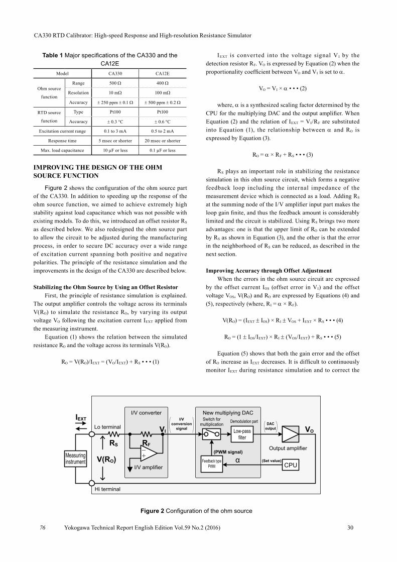
Figure 2 shows the configuration of the ohm source part of the CA330. In addition to speeding up the response of the ohm source function, we aimed to achieve extremely high stability against load capacitance which was not possible with existing models. To do this, we introduced an offset resistor RS as described below. We also redesigned the ohm source part to allow the circuit to be adjusted during the manufacturing process, in order to secure DC accuracy over a wide range of excitation current spanning both positive and negative polarities. The principle of the resistance simulation and the improvements in the design of the CA330 are described below.
Stabilizing the Ohm Source by Using an Offset ResistorFirst, the principle of resistance simulation is explained.
The output amplifier controls the voltage across its terminals V(RO) to simulate the resistance RO, by varying its output voltage VO following the excitation current IEXT applied from the measuring instrument.
Equation (1) shows the relation between the simulated resistance RO and the voltage across its terminals V(RO).
RO = V(RO)/IEXT = (VO/IEXT) + RS • • • (1)
IEXT is conver ted into the voltage signal VI by the detection resistor RF. VO is expressed by Equation (2) when the proportionality coefficient between VO and VI is set to a.
VO = VI × a • • • (2)
where, a is a synthesized scaling factor determined by the CPU for the multiplying DAC and the output amplifier. When Equation (2) and the relation of IEXT = VI/RF are substituted into Equation (1), the relationship between a and RO is expressed by Equation (3).
RO = a × RF + RS • • • (3)
RS plays an important role in stabilizing the resistance simulation in this ohm source circuit, which forms a negative feedback loop including the internal impedance of the measurement device which is connected as a load. Adding RS
at the summing node of the I/V amplifier input part makes the loop gain finite, and thus the feedback amount is considerably limited and the circuit is stabilized. Using RS brings two more advantages: one is that the upper limit of RO can be extended by RS as shown in Equation (3), and the other is that the error in the neighborhood of RS can be reduced, as described in the next section.
Improving Accuracy through Offset AdjustmentWhen the errors in the ohm source circuit are expressed
by the offset current IOS (offset error in VI) and the offset voltage VOS, V(RO) and RO are expressed by Equations (4) and (5), respectively (where, RI = a × RF).
V(RO) = (IEXT ± IOS) × RI ± VOS + IEXT × RS • • • (4)
RO = (1 ± IOS/IEXT) × RI ± (VOS/IEXT) + RS • • • (5)
Equation (5) shows that both the gain error and the offset of RO increase as IEXT decreases. It is difficult to continuously monitor IEXT during resistance simulation and to correct the
Table 1 Major specifications of the CA330 and the CA12E
Model CA330 CA12E
Ohm source
function
Range 500 W 400 W
Resolution 10 mW 100 mW
Accuracy ± 250 ppm ± 0.1 W ± 500 ppm ± 0.2 W
RTD source
function
Type Pt100 Pt100
Accuracy ± 0.3 °C ± 0.6 °C
Excitation current range 0.1 to 3 mA 0.5 to 2 mA
Response time 5 msec or shorter 20 msec or shorter
Max. load capacitance 10 µF or less 0.1 µF or less
Figure 2 Configuration of the ohm source
IEXT
Feedback type PWM
V(RO) +−RF RS
Low-pass filter
Output amplifier
I/V amplifier
Measuring instrument CPU
VO VI
α
Demodulation part
I/V converter
Lo terminal
Hi terminal
New multiplying DAC Switch for
multiplication
(Set value)
(PWM signal)
I/V conversion
signal DAC
output
CA330 RTD Calibrator: High-speed Response and High-resolution Resistance Simulator
Yokogawa Technical Report English Edition Vol.59 No.2 (2016)
errors by real-time calculation using the known correction values of IOS and VOS. However, when IOS and VOS are eliminated, the effect of these errors which become prominent as IEXT decreases can be alleviated. Therefore, we decided to adjust the offset in the manufacturing process to eliminate IOS and VOS as described below.
To eliminate IOS and VOS, the offset voltages of the output amplifier and the I/V amplifier (Figure 2) are respectively adjusted. In order to measure V(RO), it is necessary to use a high-accuracy measurement device that can stably handle 1 µV. First, V(RO) is measured at the condition of IEXT = 0 and RI = 0. Based on Equation (4), a correction voltage is applied to the input part of the output amplifier so that V(RO) is equal to 0 V to eliminate VOS. Then, V(RO) is measured again at the setting of IEXT = 0 and RI is equal to the full scale of the resistor value to be simulated. Based on Equation (4), V(RO) is equal to ±IOS × RI. A correction voltage is applied to the input part of the IV amplifier so that V(RO) is equal to 0 V to eliminate IOS. The CA330 automatically carries out this adjustment by using the digital to analog converter (DAC) resource installed in a programmable logic device, which is described later.
The final DC accuracy of the ohm source circuit can be aggregated into the offset drift in the output amplifier and the IV amplifier, and the stability of RF and RS. Therefore, low-drift chopper amplifiers and highly stable metal foil resistors are installed in the CA330. As shown in Equation (5), these errors are minimized when RI = 0, that is, RO = RS. Thus, the accuracy of the resistance to be simulated can be improved in most calibration practices by selecting RS close to the resistance value that is frequently selected for calibration.
Speeding Up Multiplying DACThe multiplying DAC is composed of a feedback type
PWM, a switch for multiplication that determines the carrier amplitude, and a demodulation part for converting PWM signals into analog signals (Figure 2). During resistance simulation, the amplitude VI of the carrier varies following IEXT. The section integration type demodulation method used in conventional models cannot carry out demodulation at high
speed because the tracking speed against changes in IEXT is limited by the cycle of carrier frequency, which is described below. To solve this problem, we aimed to raise the carrier frequency by using a simple low-pass filter.
Carrier frequency and PWM resolution are in a trade-off relationship, and the PWM resolution is determined by the ratio of carrier frequency to PWM operating frequency. To obtain a resolution of 20 bits at the carrier frequency of 10 kHz, the PWM operating frequency must be 10 GHz or higher, which is difficult to achieve. Yokogawa has already developed a high-precision AD converter using the feedback type PWM (1). We use it as the multiplying DAC of the CA330 and improved it with digital signal processing technology in order to ensure high resolution at a low operating frequency.
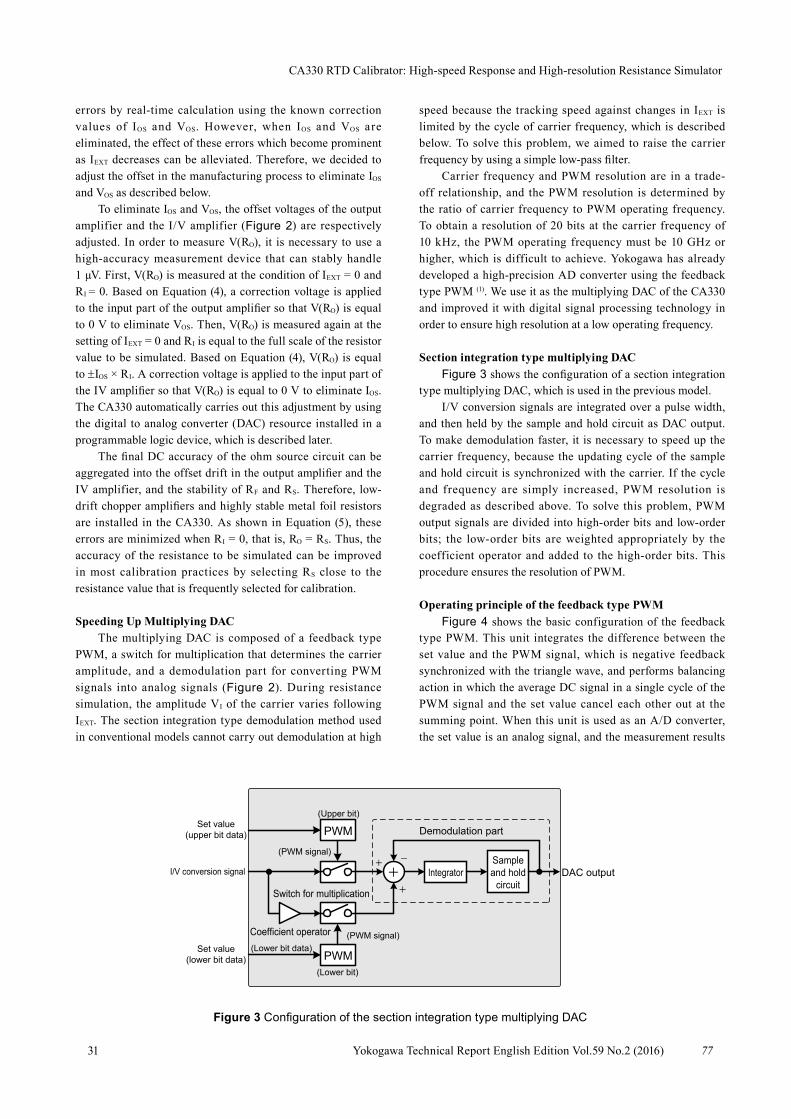
Section integration type multiplying DACFigure 3 shows the configuration of a section integration
type multiplying DAC, which is used in the previous model.I/V conversion signals are integrated over a pulse width,
and then held by the sample and hold circuit as DAC output. To make demodulation faster, it is necessary to speed up the carrier frequency, because the updating cycle of the sample and hold circuit is synchronized with the carrier. If the cycle and frequency are simply increased, PWM resolution is degraded as described above. To solve this problem, PWM output signals are divided into high-order bits and low-order bits; the low-order bits are weighted appropriately by the coefficient operator and added to the high-order bits. This procedure ensures the resolution of PWM.
Operating principle of the feedback type PWMFigure 4 shows the basic configuration of the feedback
type PWM. This unit integrates the difference between the set value and the PWM signal, which is negative feedback synchronized with the triangle wave, and performs balancing action in which the average DC signal in a single cycle of the PWM signal and the set value cancel each other out at the summing point. When this unit is used as an A/D converter, the set value is an analog signal, and the measurement results
31 77
Figure 3 Configuration of the section integration type multiplying DAC
+ + Integrator
Sample and hold
circuit
−
PWM
Switch for multiplication
Demodulation part
I/V conversion signal DAC output
PWM
+
Coefficient operator
(Upper bit)
(Lower bit)
Set value (upper bit data)
(Lower bit data)
(PWM signal)
(PWM signal) Set value
(lower bit data)

CA330 RTD Calibrator: High-speed Response and High-resolution Resistance Simulator
Yokogawa Technical Report English Edition Vol.59 No.2 (2016)
(digital value) that are synchronized with the cycle of carrier frequency are obtained by counting the pulse widths of PWM signals.
Figure 4 Basic configuration of the feedback type PWM
Improved feedback type PWMFigure 5 shows the configuration of the improved
feedback type PWM, which emulates operations by digital signal processing in the CA330. A major difference between the PWMs of Figure 4 and Figure 5 is that, in the latter, the PWM signal negatively fed back to the summing point of the input part is updated in synchronization with the PWM operating frequency. As a result, the duty ratio of the PWM signal is quantized, and the PWM unit performs the balancing action following the operating frequency so that the average value of the PWM output in each feedback matches the set value.
Figure 6 shows an example of comparison process waveforms at points (a) through (f) in Figure 5. By outputting two identical triangle waves which are 180 degrees out of phase, the carrier frequency is doubled, and ripple noise can be reduced at a low-pass filter in the subsequent stage.
Figure 6 Example of comparison process waveforms in Figure 5
In the high-frequency region, because the input value is negatively fed back after the integration process, the amount of feedback decreases. In contrast, because the quantization noise created by the comparison processing is negatively fed back without being integrated, the loop gain increases relatively. In the low-frequency region, the gain of the quantization noise is suppressed by the feedback of the input value. As a result, the quantization noise is pushed toward the high-frequency region. This effect is called the noise shaping effect, and the noise-shaped quantization noise can be eliminated through a low-pass filter.
Improved feedback type PWM performs the integration process twice before the comparison process to obtain the second-order noise shaping effect on the quantization noise, ensuring the S/N ratio required to increase the PWM resolution. In addition, noise reduction is also expected by the shift of idle tones toward the high-frequency region (idle tone is noise that is created depending on the integration time required for the state transition of the comparison results).
Figure 7 shows the results of simulating frequency characteristics by discrete Fourier transform, at the input of AC signals. It can be seen that quantization noise is pushed toward the high-frequency region.
Comparator
+
−
PWM signal + 0,1
Level converter
Triangle wave generator
Integrator Set value
1 0
−fullscale +fullscale
0 1
(a) (b)
(c)
(d)
(e)
(f)
3278
Figure 5 Configuration of the improved feedback type PWM
= kTriangle wave cycle
Data update rate
Comparison
+
−
+
+PWM signal
−PWM signal
+ +
+
+ +
(a)
(b)
(c)
(d)
(e)
(f)
Integration Integration × k
Inversion Triangle wave
Comparison
Level conversion
Level conversion +
0,1
0,1
Set value

CA330 RTD Calibrator: High-speed Response and High-resolution Resistance Simulator
Yokogawa Technical Report English Edition Vol.59 No.2 (2016)
Figure 7 Simulated frequency characteristics of the quantization noise
Integrating FunctionsArithmetic processes for PWM are carried out by an
arithmetic logic unit on a programmable system on chip (SoC), and a programmable logic device (PLD) on the same chip was used to build a state machine and glue logics for its control. SoC also has a DS modulator and high-performance digital filters, which provide a resistance measuring function with high resolution. Furthermore, this device has various analog components that can reinforce the functions of external circuits such as LCD driver, comparator, and DAC. Thus, SoC is used as the optimum device for the CA330, which has many functions packed in a small body.
RESULTS OF CHARACTERISTICS EVALUATION
Figure 8 shows measurement data in the 500 W range.
Figure 8 Measurement data in the 500 W range
This data shows that the CA330 has excellent precision of up to 30 mW resolution and linearity, which is necessary to simulate RTDs, over the specification range of both IEXT and resistance.
Figure 9 shows response waveforms of output voltage in simulating 400 W, when IEXT of 1 mA is applied stepwise. The response speed of the CA330 is remarkably improved compared with the CA12E, thanks to the faster demodulation process of PWM. The output waveform of the CA12E shows a stepwise pattern with long response time because its section integration type multiplying DAC can only follow changes in IEXT at the updating intervals of the sample and hold circuit.
Figure 9 Response waveforms on generating 400 W
CONCLUSION
Although the CA330 resembles the previous CA12E model, users wil l clearly not ice huge dif ferences in performance.
Remarkable improvement in the stability and responsivity of the ohm source function makes the function behave more closely to the actual resistor. We believe that the CA330 is an ideal calibrator for measuring instruments.
In this development, we established technologies for integrating high-resolution measurement and generation functions onto a single chip. This will help Yokogawa develop more sophisticated handheld measurement devices.
REFERENCES
(1) Tomoyuki Tanabe, Yoshio Oguma, et al., “Integrated Type Digital Voltmeter,” Yokogawa Technical Report, Vol. 11, No. 5, 1967, pp. 94-107 (in Japanese)
−200
−180
−160
−140
−120
−100
−80
−60
−40
−20
0
0.000001 0.00001 0.0001 0.001 0.01 0.1
Qua
ntiz
atio
n no
ise
[dB
]
Normalized frequency [Hz]
Input signal
−100
−80
−60
−40
−20
0
20
40
60
80
100
0 100 200 300 400 500
Err
or [m
Ω]
Set resistance [Ω]
IEXT = +100 µA IEXT = +3 mA
IEXT = −3 mA IEXT = −100 µA
CA330
Vol
tage
CA12E
1 msec/div
100
mV
/div
Time
33 79

CA330 RTD Calibrator: High-speed Response and High-resolution Resistance Simulator
Yokogawa Technical Report English Edition Vol.59 No.2 (2016) 3480
Related Documents


