© KEMET Electronics Corporation • P.O. Box 5928 • Greenville, SC 29606 (864) 963-6300 • www.kemet.com C1002_X7R_SMD • 9/20/2013 1 One world. One KEMET Benefits • -55°C to +125°C operating temperature range • Pb-Free and RoHS Compliant • Temperature stable dielectric • EIA 0402, 0603, 0805, 1206, 1210, 1808, 1812, 1825, 2220, and 2225 case sizes • DC voltage ratings of 6.3 V, 10 V, 16 V, 25 V, 50 V, 100 V, 200 V, and 250 V • Capacitance offerings ranging from 10 pF to 47 μF • Available capacitance tolerances of ±5%, ±10%, and ±20% • Non-polar device, minimizing installation concerns • 100% pure matte tin-plated termination finish allowing for excellent solderability • SnPb termination finish option available upon request (5% minimum) Applications Typical applications include decoupling, bypass, filtering and transient voltage suppression. Overview KEMET’s X7R dielectric features a 125°C maximum operating temperature and is considered “temperature stable.” The Electronics Components, Assemblies & Materials Association (EIA) characterizes X7R dielectric as a Class II material. Components of this classification are fixed, ceramic dielectric capacitors suited for bypass and decoupling applications or for frequency discriminating circuits where Q and stability of capacitance characteristics are not critical. X7R exhibits a predictable change in capacitance with respect to time and voltage and boasts a minimal change in capacitance with reference to ambient temperature. Capacitance change is limited to ±15% from -55°C to +125°C. Surface Mount Multilayer Ceramic Chip Capacitors (SMD MLCCs) X7R Dielectric, 6.3 – 250 VDC (Commercial Grade) Ordering Information C 1206 C 106 M 4 R A C TU Ceramic Case Size (L" x W") Specification/ Series 1 Capacitance Code (pF) Capacitance Tolerance Voltage Dielectric Failure Rate/ Design Termination Finish 2 Packaging/Grade (C-Spec) 3 0402 0603 0805 1206 1210 1808 1812 1825 2220 2225 C = Standard 2 Significant Digits + Number of Zeros J = ±5% K = ±10% M = ±20% 9 = 6.3 V 8 = 10 V 4 = 16 V 3 = 25 V 6 = 35 V 5 = 50 V 1 = 100 V 2 = 200 V A = 250 V R = X7R A = N/A C = 100% Matte Sn Blank = Bulk TU = 7" Reel Unmarked TM = 7" Reel Marked 1 Flexible termination option is available. Please see FT-CAP product bulletin C1013_X7R_FT-CAP_SMD. 2 Additional termination finish options may be available. Contact KEMET for details. 3 Additional reeling or packaging options may be available. Contact KEMET for details.

Welcome message from author
This document is posted to help you gain knowledge. Please leave a comment to let me know what you think about it! Share it to your friends and learn new things together.
Transcript
© KEMET Electronics Corporation • P.O. Box 5928 • Greenville, SC 29606 (864) 963-6300 • www.kemet.com C1002_X7R_SMD • 9/20/2013 1One world. One KEMET
Benefits
• -55°C to +125°C operating temperature range• Pb-Free and RoHS Compliant• Temperature stable dielectric• EIA 0402, 0603, 0805, 1206, 1210, 1808, 1812, 1825, 2220,
and 2225 case sizes• DC voltage ratings of 6.3 V, 10 V, 16 V, 25 V, 50 V, 100 V,
200 V, and 250 V• Capacitanceofferingsrangingfrom10pFto47μF• Available capacitance tolerances of ±5%, ±10%, and ±20% • Non-polar device, minimizing installation concerns• 100%puremattetin-platedterminationfinishallowingfor
excellent solderability• SnPbterminationfinishoptionavailableuponrequest
(5% minimum)
Applications
Typicalapplicationsincludedecoupling,bypass,filteringandtransient voltage suppression.
Overview
KEMET’s X7R dielectric features a 125°C maximum operating temperatureandisconsidered“temperaturestable.”TheElectronics Components, Assemblies & Materials Association (EIA)characterizesX7RdielectricasaClassIImaterial.Componentsofthisclassificationarefixed,ceramicdielectriccapacitors suited for bypass and decoupling applications
orforfrequencydiscriminatingcircuitswhereQandstabilityofcapacitancecharacteristicsarenotcritical.X7Rexhibitsapredictablechangeincapacitancewithrespecttotimeandvoltageandboastsaminimalchangeincapacitancewithreferencetoambienttemperature.Capacitancechangeislimitedto±15%from-55°C to +125°C.
SurfaceMountMultilayerCeramicChipCapacitors(SMDMLCCs)
X7R Dielectric, 6.3 – 250 VDC (Commercial Grade)
Ordering Information
C 1206 C 106 M 4 R A C TU
Ceramic Case Size (L"xW")
Specification/Series1
Capacitance Code (pF)
Capacitance Tolerance Voltage Dielectric Failure Rate/
Design TerminationFinish2 Packaging/Grade (C-Spec)3
0402060308051206121018081812182522202225
C = Standard 2SignificantDigits + Number
of Zeros
J = ±5%K = ±10%M = ±20%
9 = 6.3 V8 = 10 V4 = 16 V3 = 25 V6 = 35 V5 = 50 V1 = 100 V2 = 200 VA = 250 V
R = X7R A = N/A C = 100% Matte Sn Blank = BulkTU=7"ReelUnmarkedTM=7"ReelMarked
1 Flexible termination option is available. Please see FT-CAP product bulletin C1013_X7R_FT-CAP_SMD.2 Additional termination finish options may be available. Contact KEMET for details.3 Additional reeling or packaging options may be available. Contact KEMET for details.
© KEMET Electronics Corporation • P.O. Box 5928 • Greenville, SC 29606 (864) 963-6300 • www.kemet.com C1002_X7R_SMD • 9/20/2013 2
Surface Mount Multilayer Ceramic Chip Capacitors (SMD MLCCs) – X7R Dielectric, 6.3 – 250 VDC (Commercial Grade)
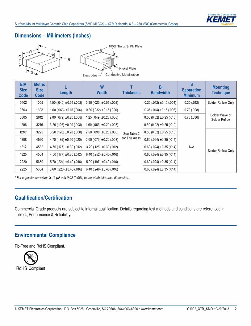
Dimensions – Millimeters (Inches)
Cer
amic
Su
rfac
e M
ou
nt
W L
T B
S
100% Tin or SnPb Plate
Nickel Plate
Conductive MetalizationElectrodes
EIA Size Code
Metric Size Code
L Length
W Width
T Thickness
B Bandwidth
SSeparation Minimum
Mounting Technique
0402 1005 1.00 (.040) ±0.05 (.002) 0.50 (.020) ±0.05 (.002)
See Table 2forThickness
0.30 (.012) ±0.10 (.004) 0.30 (.012) SolderReflowOnly
0603 1608 1.60 (.063) ±0.15 (.006) 0.80 (.032) ±0.15 (.006) 0.35 (.014) ±0.15 (.006) 0.70 (.028)SolderWaveorSolderReflow0805 2012 2.00 (.079) ±0.20 (.008) 1.25 (.049) ±0.20 (.008) 0.50 (0.02) ±0.25 (.010) 0.75 (.030)
1206 3216 3.20 (.126) ±0.20 (.008) 1.60 (.063) ±0.20 (.008) 0.50 (0.02) ±0.25 (.010)
N/A
12101 3225 3.20 (.126) ±0.20 (.008) 2.50 (.098) ±0.20 (.008) 0.50 (0.02) ±0.25 (.010)
SolderReflowOnly
1808 4520 4.70 (.185) ±0.50 (.020) 2.00 (.079) ±0.20 (.008) 0.60 (.024) ±0.35 (.014)
1812 4532 4.50 (.177) ±0.30 (.012) 3.20 (.126) ±0.30 (.012) 0.60 (.024) ±0.35 (.014)
1825 4564 4.50 (.177) ±0.30 (.012) 6.40 (.252) ±0.40 (.016) 0.60 (.024) ±0.35 (.014)
2220 5650 5.70 (.224) ±0.40 (.016) 5.00 (.197) ±0.40 (.016) 0.60 (.024) ±0.35 (.014)
2225 5664 5.60 (.220) ±0.40 (.016) 6.40 (.248) ±0.40 (.016) 0.60 (.024) ±0.35 (.014)
1 For capacitance values ≥ 12 µF add 0.02 (0.001) to the width tolerance dimension.
Qualification/Certification
CommercialGradeproductsaresubjecttointernalqualification.Detailsregardingtestmethodsandconditionsarereferencedin Table 4, Performance & Reliability.
Environmental Compliance
Pb-Free and RoHS Compliant.
© KEMET Electronics Corporation • P.O. Box 5928 • Greenville, SC 29606 (864) 963-6300 • www.kemet.com C1002_X7R_SMD • 9/20/2013 3
Surface Mount Multilayer Ceramic Chip Capacitors (SMD MLCCs) – X7R Dielectric, 6.3 – 250 VDC (Commercial Grade)
Electrical Parameters/Characteristics
Item Parameters/CharacteristicsOperating Temperature Range -55°C to +125°C
CapacitanceChangewithReferenceto+25°Cand0VDCApplied(TCC) ±15%
AgingRate(Maximum%CapacitanceLoss/DecadeHour) 3.0%
DielectricWithstandingVoltage(DWV) 250% of rated voltage(5±1secondandcharge/dischargenotexceeding50mA)
DissipationFactor(DF)MaximumLimit@25ºC SeeDissipationFactor(DF)LimitsTable
InsulationResistance(IR)Limit@25°C SeeInsulationResistanceLimitTable(Ratedvoltageappliedfor120±5seconds@25°C)
Regarding aging rate: Capacitance measurements (including tolerance) are indexed to a referee time of 48 or 1,000 hours. Please refer to a part number specific datasheet for referee time details. To obtain IR limit, divide MΩ-µF value by the capacitance and compare to GΩ limit. Select the lower of the two limits.Capacitance and dissipation factor (DF) measured under the following conditions: 1 kHz ±50 Hz and 1.0 ±0.2 Vrms if capacitance ≤ 10 µF 120 Hz ±10 Hz and 0.5 ±0.1 Vrms if capacitance > 10 µFNote: When measuring capacitance it is important to ensure the set voltage level is held constant. The HP4284 and Agilent E4980 have a feature known as Automatic Level Control (ALC). The ALC feature should be switched to "ON."
Insulation Resistance Limit Table (X7R Dielectric)
EIA Case Size 1,000 Megohm Microfarads or 100 GΩ
500 Megohm Microfarads or 10 GΩ
0201 N/A ALL
0402 < 0.012 µF ≥0.012µF
0603 < 0.047 µF ≥0.047µF
0805 < 0.047 µF ≥0.047µF
1206 < 0.22 µF ≥0.22µF
1210 < 0.39 µF ≥0.39µF
1808 ALL N/A
1812 < 2.2 µF ≥2.2µF
1825 ALL N/A
2220 < 10 µF ≥10µF
2225 ALL N/A
© KEMET Electronics Corporation • P.O. Box 5928 • Greenville, SC 29606 (864) 963-6300 • www.kemet.com C1002_X7R_SMD • 9/20/2013 4
Surface Mount Multilayer Ceramic Chip Capacitors (SMD MLCCs) – X7R Dielectric, 6.3 – 250 VDC (Commercial Grade)
Dissipation Factor (DF) Limits Table
EIA Case Size
Rated DC Voltage Capacitance Dissipation
Factor
0402
< 16
All
5.0%
16/25 3.5%
> 25 2.5%
0603
< 16
< 1.0 uF
5.0%
16/25 3.5%
> 25 2.5%
< 16≥1.0uF 10.0%
16/25
0805
< 16≤2.2µF
5.0%
16/25 3.5%
> 25 < 1.0 µF 2.5%
< 16> 2.2 µF
10.0%16/25
> 25 ≥1.0µF
1206
< 16
< 10 µF
5.0%
16/25 3.5%
> 25 2.5%
< 16≥10µF 10.0%
16/25
1210
< 16
< 22 µF
5.0%
16/25 3.5%
> 25 2.5%
< 16≥22µF 10.0%
16/25
1812 – 2225
< 16
All
5.0%
16/25 3.5%
> 25 2.5%
© KEMET Electronics Corporation • P.O. Box 5928 • Greenville, SC 29606 (864) 963-6300 • www.kemet.com C1002_X7R_SMD • 9/20/2013 5
Surface Mount Multilayer Ceramic Chip Capacitors (SMD MLCCs) – X7R Dielectric, 6.3 – 250 VDC (Commercial Grade)
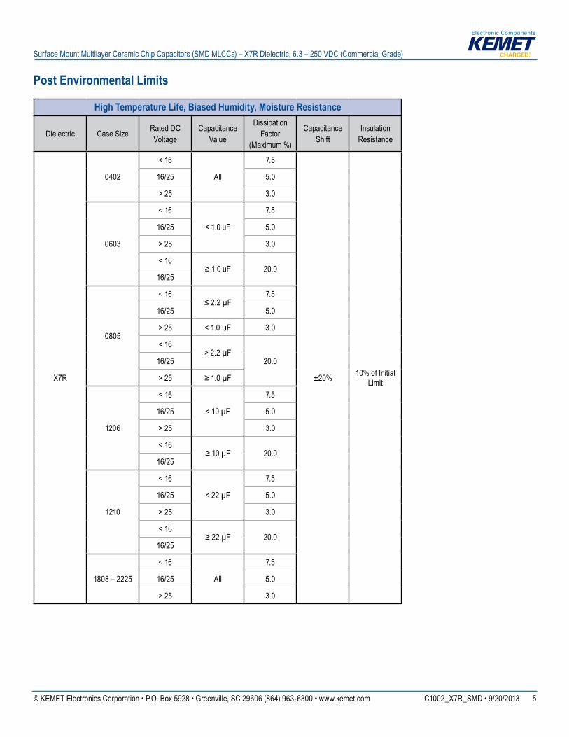
Post Environmental Limits
High Temperature Life, Biased Humidity, Moisture Resistance
Dielectric Case Size Rated DC Voltage
Capacitance Value
Dissipation Factor
(Maximum %)
Capacitance Shift
Insulation Resistance
X7R
0402
< 16
All
7.5
±20% 10% of Initial Limit
16/25 5.0
> 25 3.0
0603
< 16
< 1.0 uF
7.5
16/25 5.0
> 25 3.0
< 16≥1.0uF 20.0
16/25
0805
< 16≤2.2µF
7.5
16/25 5.0
> 25 < 1.0 µF 3.0
< 16> 2.2 µF
20.016/25
> 25 ≥1.0µF
1206
< 16
< 10 µF
7.5
16/25 5.0
> 25 3.0
< 16≥10µF 20.0
16/25
1210
< 16
< 22 µF
7.5
16/25 5.0
> 25 3.0
< 16≥22µF 20.0
16/25
1808 – 2225
< 16
All
7.5
16/25 5.0
> 25 3.0
© KEMET Electronics Corporation • P.O. Box 5928 • Greenville, SC 29606 (864) 963-6300 • www.kemet.com C1002_X7R_SMD • 9/20/2013 6
Surface Mount Multilayer Ceramic Chip Capacitors (SMD MLCCs) – X7R Dielectric, 6.3 – 250 VDC (Commercial Grade)
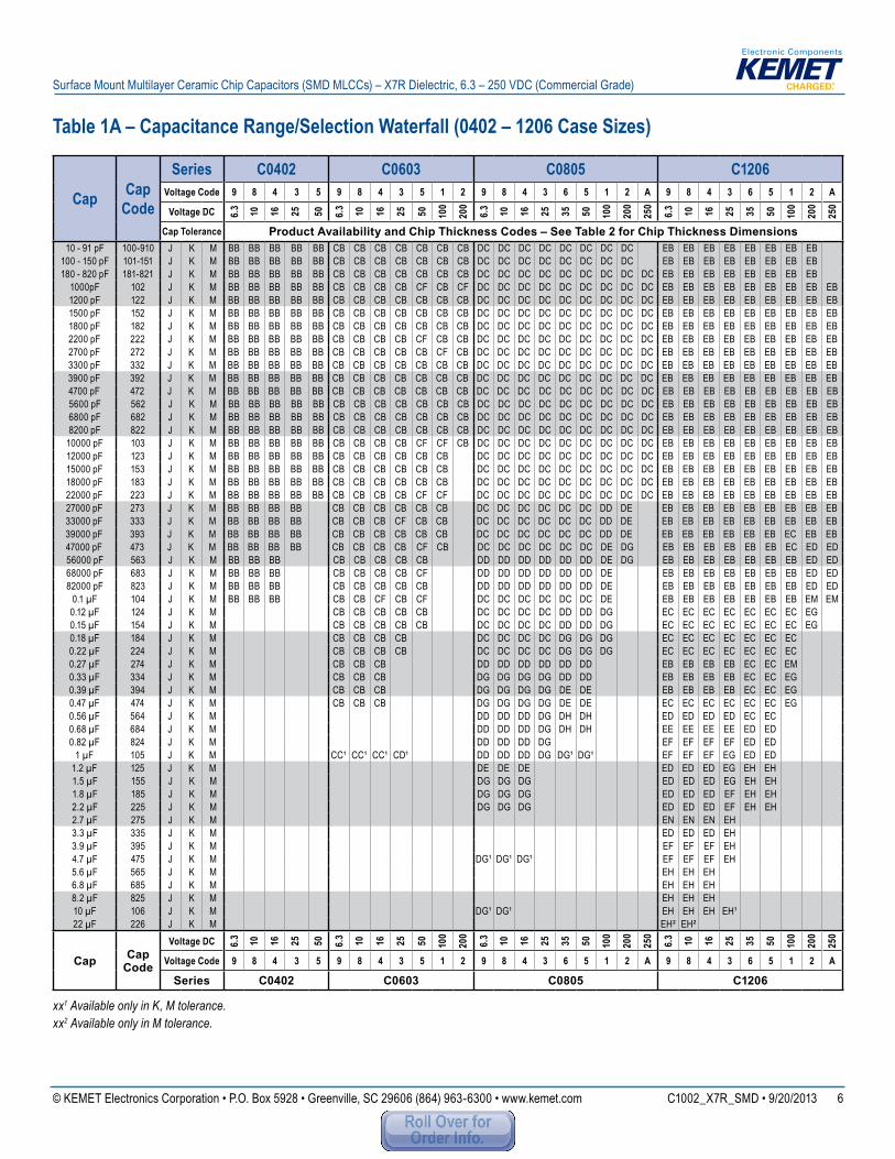
Table 1A – Capacitance Range/Selection Waterfall (0402 – 1206 Case Sizes)
Cap Cap Code
Series C0402 C0603 C0805 C1206Voltage Code 9 8 4 3 5 9 8 4 3 5 1 2 9 8 4 3 6 5 1 2 A 9 8 4 3 6 5 1 2 A
Voltage DC 6.3 10 16 25 50 6.3 10 16 25 50 100
200
6.3 10 16 25 35 50 100
200
250
6.3 10 16 25 35 50 100
200
250
Cap Tolerance Product Availability and Chip Thickness Codes – See Table 2 for Chip Thickness Dimensions10 - 91 pF 100-910 J K M BB BB BB BB BB CB CB CB CB CB CB CB DC DC DC DC DC DC DC DC EB EB EB EB EB EB EB EB
100 - 150 pF 101-151 J K M BB BB BB BB BB CB CB CB CB CB CB CB DC DC DC DC DC DC DC DC EB EB EB EB EB EB EB EB180 - 820 pF 181-821 J K M BB BB BB BB BB CB CB CB CB CB CB CB DC DC DC DC DC DC DC DC DC EB EB EB EB EB EB EB EB
1000pF 102 J K M BB BB BB BB BB CB CB CB CB CF CB CF DC DC DC DC DC DC DC DC DC EB EB EB EB EB EB EB EB EB1200 pF 122 J K M BB BB BB BB BB CB CB CB CB CB CB CB DC DC DC DC DC DC DC DC DC EB EB EB EB EB EB EB EB EB1500 pF 152 J K M BB BB BB BB BB CB CB CB CB CB CB CB DC DC DC DC DC DC DC DC DC EB EB EB EB EB EB EB EB EB1800 pF 182 J K M BB BB BB BB BB CB CB CB CB CB CB CB DC DC DC DC DC DC DC DC DC EB EB EB EB EB EB EB EB EB2200 pF 222 J K M BB BB BB BB BB CB CB CB CB CF CB CB DC DC DC DC DC DC DC DC DC EB EB EB EB EB EB EB EB EB2700 pF 272 J K M BB BB BB BB BB CB CB CB CB CB CF CB DC DC DC DC DC DC DC DC DC EB EB EB EB EB EB EB EB EB3300 pF 332 J K M BB BB BB BB BB CB CB CB CB CB CB CB DC DC DC DC DC DC DC DC DC EB EB EB EB EB EB EB EB EB3900 pF 392 J K M BB BB BB BB BB CB CB CB CB CB CB CB DC DC DC DC DC DC DC DC DC EB EB EB EB EB EB EB EB EB4700 pF 472 J K M BB BB BB BB BB CB CB CB CB CB CB CB DC DC DC DC DC DC DC DC DC EB EB EB EB EB EB EB EB EB5600 pF 562 J K M BB BB BB BB BB CB CB CB CB CB CB CB DC DC DC DC DC DC DC DC DC EB EB EB EB EB EB EB EB EB6800 pF 682 J K M BB BB BB BB BB CB CB CB CB CB CB CB DC DC DC DC DC DC DC DC DC EB EB EB EB EB EB EB EB EB8200 pF 822 J K M BB BB BB BB BB CB CB CB CB CB CB CB DC DC DC DC DC DC DC DC DC EB EB EB EB EB EB EB EB EB
10000 pF 103 J K M BB BB BB BB BB CB CB CB CB CF CF CB DC DC DC DC DC DC DC DC DC EB EB EB EB EB EB EB EB EB12000 pF 123 J K M BB BB BB BB BB CB CB CB CB CB CB DC DC DC DC DC DC DC DC DC EB EB EB EB EB EB EB EB EB15000 pF 153 J K M BB BB BB BB BB CB CB CB CB CB CB DC DC DC DC DC DC DC DC DC EB EB EB EB EB EB EB EB EB18000 pF 183 J K M BB BB BB BB BB CB CB CB CB CB CB DC DC DC DC DC DC DC DC DC EB EB EB EB EB EB EB EB EB22000 pF 223 J K M BB BB BB BB BB CB CB CB CB CF CF DC DC DC DC DC DC DC DC DC EB EB EB EB EB EB EB EB EB27000 pF 273 J K M BB BB BB BB CB CB CB CB CB CB DC DC DC DC DC DC DD DE EB EB EB EB EB EB EB EB EB33000 pF 333 J K M BB BB BB BB CB CB CB CF CB CB DC DC DC DC DC DC DD DE EB EB EB EB EB EB EB EB EB39000 pF 393 J K M BB BB BB BB CB CB CB CB CB CB DC DC DC DC DC DC DD DE EB EB EB EB EB EB EC EB EB47000 pF 473 J K M BB BB BB BB CB CB CB CB CF CB DC DC DC DC DC DC DE DG EB EB EB EB EB EB EC ED ED56000 pF 563 J K M BB BB BB CB CB CB CB CB DD DD DD DD DD DD DE DG EB EB EB EB EB EB EB ED ED68000 pF 683 J K M BB BB BB CB CB CB CB CF DD DD DD DD DD DD DE EB EB EB EB EB EB EB ED ED82000 pF 823 J K M BB BB BB CB CB CB CB CB DD DD DD DD DD DD DE EB EB EB EB EB EB EB ED ED
0.1 µF 104 J K M BB BB BB CB CB CF CB CF DC DC DC DC DC DC DE EB EB EB EB EB EB EB EM EM0.12 µF 124 J K M CB CB CB CB CB DC DC DC DC DD DD DG EC EC EC EC EC EC EC EG0.15 µF 154 J K M CB CB CB CB CB DC DC DC DC DD DD DG EC EC EC EC EC EC EC EG0.18 µF 184 J K M CB CB CB CB DC DC DC DC DG DG DG EC EC EC EC EC EC EC0.22 µF 224 J K M CB CB CB CB DC DC DC DC DG DG DG EC EC EC EC EC EC EC0.27 µF 274 J K M CB CB CB DD DD DD DD DD DD EB EB EB EB EC EC EM0.33 µF 334 J K M CB CB CB DG DG DG DG DD DD EB EB EB EB EC EC EG0.39 µF 394 J K M CB CB CB DG DG DG DG DE DE EB EB EB EB EC EC EG0.47 µF 474 J K M CB CB CB DG DG DG DG DE DE EC EC EC EC EC EC EG0.56 µF 564 J K M DD DD DD DG DH DH ED ED ED ED EC EC0.68 µF 684 J K M DD DD DD DG DH DH EE EE EE EE ED ED0.82 µF 824 J K M DD DD DD DG EF EF EF EF ED ED
1 µF 105 J K M CC¹ CC¹ CC¹ CD¹ DD DD DD DG DG¹ DG¹ EF EF EF EG ED ED1.2 µF 125 J K M DE DE DE ED ED ED EG EH EH1.5 µF 155 J K M DG DG DG ED ED ED EG EH EH1.8 µF 185 J K M DG DG DG ED ED ED EF EH EH2.2 µF 225 J K M DG DG DG ED ED ED EF EH EH2.7 µF 275 J K M EN EN EN EH3.3 µF 335 J K M ED ED ED EH3.9 µF 395 J K M EF EF EF EH4.7 µF 475 J K M DG¹ DG¹ DG¹ EF EF EF EH5.6 µF 565 J K M EH EH EH6.8 µF 685 J K M EH EH EH8.2 µF 825 J K M EH EH EH10 µF 106 J K M DG¹ DG¹ EH EH EH EH¹22 µF 226 J K M EH² EH²
Cap Cap Code
Voltage DC 6.3 10 16 25 50 6.3 10 16 25 50 100
200
6.3 10 16 25 35 50 100
200
250
6.3 10 16 25 35 50 100
200
250
Voltage Code 9 8 4 3 5 9 8 4 3 5 1 2 9 8 4 3 6 5 1 2 A 9 8 4 3 6 5 1 2 A
Series C0402 C0603 C0805 C1206
xx1 Available only in K, M tolerance.xx2 Available only in M tolerance.
© KEMET Electronics Corporation • P.O. Box 5928 • Greenville, SC 29606 (864) 963-6300 • www.kemet.com C1002_X7R_SMD • 9/20/2013 7
Surface Mount Multilayer Ceramic Chip Capacitors (SMD MLCCs) – X7R Dielectric, 6.3 – 250 VDC (Commercial Grade)
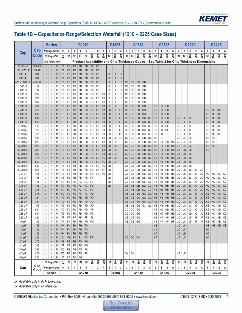
Table 1B – Capacitance Range/Selection Waterfall (1210 – 2225 Case Sizes)
xx1 Available only in K, M tolerance.xx2 Available only in M tolerance.
Cap Cap Code
Series C1210 C1808 C1812 C1825 C2220 C2225Voltage Code 9 8 4 3 5 1 2 A 5 1 2 3 5 1 2 A 5 1 2 A 3 5 1 2 A 5 1 2 A
Voltage DC 6.3 10 16 25 50 100
200
250
50 100
200
25 50 100
200
250
50 100
200
250
25 50 100
200
250
50 100
200
250
Cap Tolerance Product Availability and Chip Thickness Codes – See Table 2 for Chip Thickness Dimensions10 - 91 pF 100-910 J K M FB FB FB FB FB FB FB
100 - 270 pF 101-271 J K M FB FB FB FB FB FB FB330 pF 331 J K M FB FB FB FB FB FB FB LF LF LF390 pF 391 J K M FB FB FB FB FB FB FB LF LF LF
470 - 1,200 pF 471-122 J K M FB FB FB FB FB FB FB LF LF LF GB GB GB GB1,500 pF 152 J K M FB FB FB FB FB FB FE LF LF LF GB GB GB GB1,800 pF 182 J K M FB FB FB FB FB FB FE LF LF LF GB GB GB GB2,200 pF 222 J K M FB FB FB FB FB FB FB FB LF LF LF GB GB GB GB2,700 pF 272 J K M FB FB FB FB FB FB FB FB LF LF LF GB GB GB GB3,300 pF 332 J K M FB FB FB FB FB FB FB FB LF LF GB GB GB GB3,900 pF 392 J K M FB FB FB FB FB FB FB FB LF LF GB GB GB GB HB HB HB4,700 pF 472 J K M FB FB FB FB FB FB FB FB LD LD LD GB GB GB GD HB HB HB KE KE KE5,600 pF 562 J K M FB FB FB FB FB FB FB FB LD LD LD GB GB GB GH HB HB HB KE KE KE6,800 pF 682 J K M FB FB FB FB FB FB FB FB LD LD LD GB GB GB GB GB HB HB HB JE JE JE KE KE KE8,200 pF 822 J K M FB FB FB FB FB FB FB FB LD LD LD GB GB GB GB GB HB HB HB JE JE JE KE KE KE10,000 pF 103 J K M FB FB FB FB FB FB FB FB LD LD LD GB GB GB GB GB HB HB HE JE JE JE KE KE KE12,000 pF 123 J K M FB FB FB FB FB FB FB FB LD LD LD GB GB GB GB GB HB HB HE JE JE JE KE KE KE15,000 pF 153 J K M FB FB FB FB FB FB FB FB LD LD LD GB GB GB GB GB HB HB JE JE JE KE KE KE18,000 pF 183 J K M FB FB FB FB FB FB FB FB LD LD LD GB GB GB GB GB HB HE JE JE JE KE KE22,000 pF 223 J K M FB FB FB FB FB FB FB FB LD LD GB GB GB GB GB HB HB HB HB JE JE JE KE KE27,000 pF 273 J K M FB FB FB FB FB FB FB FB LD LD GB GB GB GB GB HB HB HB HB JE JE JE KE KE33,000 pF 333 J K M FB FB FB FB FB FB FB FB LD LD GB GB GB GB GB HB HB HB HB JB JB JB KE39,000 pF 393 J K M FB FB FB FB FB FB FB FB LD LD GB GB GB GB GB HB HB HB HB JB JB JB47,000 pF 473 J K M FB FB FB FB FB FB FC FC LD LD GB GB GB GB GB HB HB HB HB JB JB JB56,000 pF 563 J K M FB FB FB FB FB FB FC FC LD LD GB GB GB GB GB HB HB HB HB JB JB JB68,000 pF 683 J K M FB FB FB FB FB FB FC FC LD GB GB GB GB GB HB HB HB HB JB JB JB82,000 pF 823 J K M FB FB FB FB FB FC FF FF LD GB GB GB GB GB HB HB HB HB JC JC JC JC JC
0.10 µF 104 J K M FB FB FB FB FB FD FG FG LD GB GB GB GB GB HB HB HB HB JC JC JC JC JC KC KC KC KC0.12 µF 124 J K M FB FB FB FB FB FD LD GB GB GB GB GB HB HB HB HB JC JC JC JC JC KC KC KC KC0.15 µF 154 J K M FC FC FC FC FC FD LD GB GB GB GE GE HB HB HB HB JC JC JC JC JC KC KC KC KC0.18 µF 184 J K M FC FC FC FC FC FD LD GB GB GB GG GG HB HB HB HB JC JC JC JC JC KC KC KC KC0.22 µF 224 J K M FC FC FC FC FC FD GB GB GB GG GG HB HB HB HB JC JC JC JC JC KC KC KC KC0.27 µF 274 J K M FC FC FC FC FC FD GB GB GG GG GG HB HB HB HB JC JC JC JC JC KB KC KC KC0.33 µF 334 J K M FD FD FD FD FD FD GB GB GG GG GG HB HB HB HB JC JC JC JC JC KB KC KC KC0.39 µF 394 J K M FD FD FD FD FD FD GB GB GG GG GG HB HB HD HD JC JC JC JC JC KB KC KC KC0.47 µF 474 J K M FD FD FD FD FD FD GB GB GG GJ GJ HB HB HD HD JC JC JC JC JC KB KC KD KD0.56 µF 564 J K M FD FD FD FD FD FF GC GC GG HB HD HD HD JC JC JC JD JD KB KC KD KD0.68 µF 684 J K M FD FD FD FD FD FG GC GC GG HB HD HD HD JC JC JD JD JD KB KC KD KD0.82 µF 824 J K M FF FF FF FF FF FL GE GE GG HB HF HF HF JC JC JF JF JF KB KC KE KE1.0 µF 105 J K M FH FH FH FH FH FM GE GE GG HB HF HF HF JC JC JF JF JF KB KD KE KE1.2 µF 125 J K M FH FH FH FH FG HB JC JC KB KE KE KE1.5 µF 155 J K M FH FH FH FH FG HC JC JC KC1.8 µF 185 J K M FH FH FH FH FG HD JD JD KD2.2 µF 225 J K M FJ FJ FJ FJ FG FT¹ GO GO GO¹ HF JF JF KD2.7 µF 275 J K M FE FE FE FG FH3.3 µF 335 J K M FF FF FF FM FM3.9 µF 395 J K M FG FG FG FG FK4.7 µF 475 J K M FC FC FC FG FS GK GK JF JF5.6 µF 565 J K M FF FF FF FH
Cap Cap Code
Voltage DC 6.3 10 16 25 50 100
200
250
50 100
200
25 50 100
200
250
50 100
200
250
25 50 100
200
250
50 100
200
250
Voltage Code 9 8 4 3 5 1 2 A 5 1 2 3 5 1 2 A 5 1 2 A 3 5 1 2 A 5 1 2 A
Series C1210 C1808 C1812 C1825 C2220 C2225
© KEMET Electronics Corporation • P.O. Box 5928 • Greenville, SC 29606 (864) 963-6300 • www.kemet.com C1002_X7R_SMD • 9/20/2013 8
Surface Mount Multilayer Ceramic Chip Capacitors (SMD MLCCs) – X7R Dielectric, 6.3 – 250 VDC (Commercial Grade)
Cap Cap Code
Series C1210 C1808 C1812 C1825 C2220 C2225Voltage Code 9 8 4 3 5 1 2 A 5 1 2 3 5 1 2 A 5 1 2 A 3 5 1 2 A 5 1 2 A
Voltage DC 6.3 10 16 25 50 100
200
250
50 100
200
25 50 100
200
250
50 100
200
250
25 50 100
200
250
50 100
200
250
Cap Tolerance Product Availability and Chip Thickness Codes – See Table 2 for Chip Thickness Dimensions6.8 µF 685 J K M FG FG FG FM8.2 µF 825 J K M FH FH FH FK10 µF 106 J K M FH FH FH FS¹ GK JF JO15 µF 156 J K M FM FM JO JO22 µF 226 J K M FS FS FS² FS² JO47 µF 476 J K M FS²
Cap Cap Code
Voltage DC 6.3 10 16 25 50 100
200
250
50 100
200
25 50 100
200
250
50 100
200
250
25 50 100
200
250
50 100
200
250
Voltage Code 9 8 4 3 5 1 2 A 5 1 2 3 5 1 2 A 5 1 2 A 3 5 1 2 A 5 1 2 A
Series C1210 C1808 C1812 C1825 C2220 C2225
Table 1B – Capacitance Range/Selection Waterfall (1210 – 2225 Case Sizes) cont'd
xx1 Available only in K, M tolerance.xx2 Available only in M tolerance.
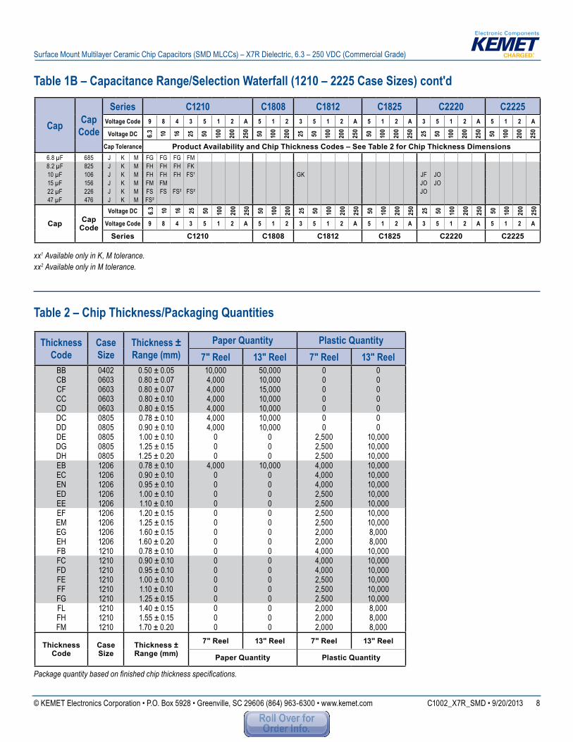
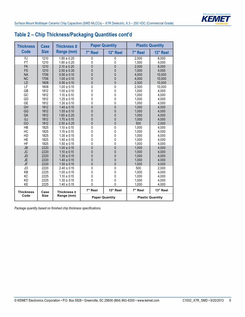
Table 2 – Chip Thickness/Packaging Quantities
Package quantity based on finished chip thickness specifications.
Thickness Code
Case Size
Thickness ± Range (mm)
Paper Quantity Plastic Quantity7" Reel 13" Reel 7" Reel 13" Reel
BB 0402 0.50 ± 0.05 10,000 50,000 0 0 CB 0603 0.80 ± 0.07 4,000 10,000 0 0 CF 0603 0.80 ± 0.07 4,000 15,000 0 0 CC 0603 0.80 ± 0.10 4,000 10,000 0 0 CD 0603 0.80 ± 0.15 4,000 10,000 0 0 DC 0805 0.78 ± 0.10 4,000 10,000 0 0 DD 0805 0.90 ± 0.10 4,000 10,000 0 0 DE 0805 1.00 ± 0.10 0 0 2,500 10,000 DG 0805 1.25 ± 0.15 0 0 2,500 10,000 DH 0805 1.25 ± 0.20 0 0 2,500 10,000 EB 1206 0.78 ± 0.10 4,000 10,000 4,000 10,000 EC 1206 0.90 ± 0.10 0 0 4,000 10,000 EN 1206 0.95 ± 0.10 0 0 4,000 10,000 ED 1206 1.00 ± 0.10 0 0 2,500 10,000 EE 1206 1.10 ± 0.10 0 0 2,500 10,000 EF 1206 1.20 ± 0.15 0 0 2,500 10,000 EM 1206 1.25 ± 0.15 0 0 2,500 10,000 EG 1206 1.60 ± 0.15 0 0 2,000 8,000 EH 1206 1.60 ± 0.20 0 0 2,000 8,000 FB 1210 0.78 ± 0.10 0 0 4,000 10,000 FC 1210 0.90 ± 0.10 0 0 4,000 10,000 FD 1210 0.95 ± 0.10 0 0 4,000 10,000 FE 1210 1.00 ± 0.10 0 0 2,500 10,000 FF 1210 1.10 ± 0.10 0 0 2,500 10,000 FG 1210 1.25 ± 0.15 0 0 2,500 10,000 FL 1210 1.40 ± 0.15 0 0 2,000 8,000 FH 1210 1.55 ± 0.15 0 0 2,000 8,000 FM 1210 1.70 ± 0.20 0 0 2,000 8,000
Thickness Code
Case Size
Thickness ± Range (mm)
7" Reel 13" Reel 7" Reel 13" Reel
Paper Quantity Plastic Quantity
© KEMET Electronics Corporation • P.O. Box 5928 • Greenville, SC 29606 (864) 963-6300 • www.kemet.com C1002_X7R_SMD • 9/20/2013 9
Surface Mount Multilayer Ceramic Chip Capacitors (SMD MLCCs) – X7R Dielectric, 6.3 – 250 VDC (Commercial Grade)
Table 2 – Chip Thickness/Packaging Quantities cont'd
Package quantity based on finished chip thickness specifications.
Thickness Code
Case Size
Thickness ± Range (mm)
Paper Quantity Plastic Quantity7" Reel 13" Reel 7" Reel 13" Reel
FJ 1210 1.85 ± 0.20 0 0 2,000 8,000 FT 1210 1.90 ± 0.20 0 0 1,500 4,000 FK 1210 2.10 ± 0.20 0 0 2,000 8,000 FS 1210 2.50 ± 0.30 0 0 1,000 4,000 NA 1706 0.90 ± 0.10 0 0 4,000 10,000 NC 1706 1.00 ± 0.15 0 0 4,000 10,000 LD 1808 0.90 ± 0.10 0 0 2,500 10,000 LF 1808 1.00 ± 0.15 0 0 2,500 10,000 GB 1812 1.00 ± 0.10 0 0 1,000 4,000 GC 1812 1.10 ± 0.10 0 0 1,000 4,000 GD 1812 1.25 ± 0.15 0 0 1,000 4,000 GE 1812 1.30 ± 0.10 0 0 1,000 4,000 GH 1812 1.40 ± 0.15 0 0 1,000 4,000 GG 1812 1.55 ± 0.10 0 0 1,000 4,000 GK 1812 1.60 ± 0.20 0 0 1,000 4,000 GJ 1812 1.70 ± 0.15 0 0 1,000 4,000 GO 1812 2.50 ± 0.20 0 0 500 2,000 HB 1825 1.10 ± 0.15 0 0 1,000 4,000 HC 1825 1.15 ± 0.15 0 0 1,000 4,000 HD 1825 1.30 ± 0.15 0 0 1,000 4,000 HE 1825 1.40 ± 0.15 0 0 1,000 4,000 HF 1825 1.50 ± 0.15 0 0 1,000 4,000 JB 2220 1.00 ± 0.15 0 0 1,000 4,000 JC 2220 1.10 ± 0.15 0 0 1,000 4,000 JD 2220 1.30 ± 0.15 0 0 1,000 4,000 JE 2220 1.40 ± 0.15 0 0 1,000 4,000 JF 2220 1.50 ± 0.15 0 0 1,000 4,000 JO 2220 2.40 ± 0.15 0 0 500 2,000 KB 2225 1.00 ± 0.15 0 0 1,000 4,000 KC 2225 1.10 ± 0.15 0 0 1,000 4,000 KD 2225 1.30 ± 0.15 0 0 1,000 4,000 KE 2225 1.40 ± 0.15 0 0 1,000 4,000
Thickness Code
Case Size
Thickness ± Range (mm)
7" Reel 13" Reel 7" Reel 13" Reel
Paper Quantity Plastic Quantity
© KEMET Electronics Corporation • P.O. Box 5928 • Greenville, SC 29606 (864) 963-6300 • www.kemet.com C1002_X7R_SMD • 9/20/2013 10
Surface Mount Multilayer Ceramic Chip Capacitors (SMD MLCCs) – X7R Dielectric, 6.3 – 250 VDC (Commercial Grade)
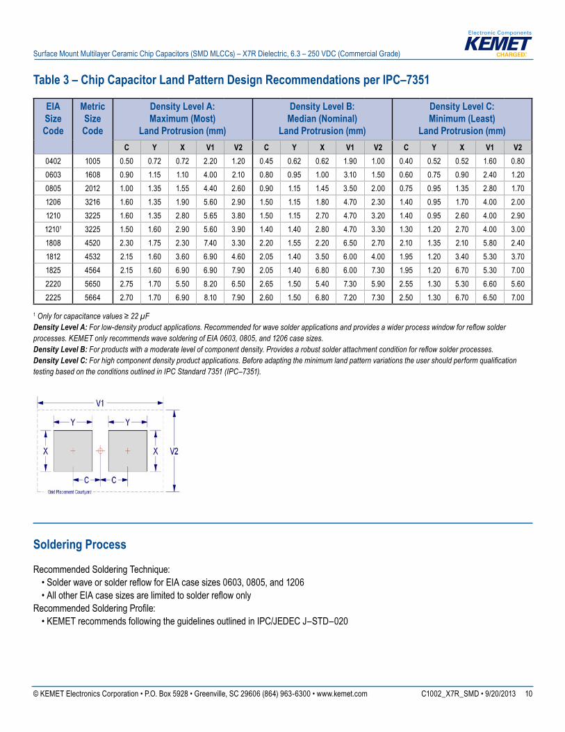
Table 3 – Chip Capacitor Land Pattern Design Recommendations per IPC–7351
EIA Size Code
Metric Size Code
Density Level A: Maximum (Most)
Land Protrusion (mm)
Density Level B: Median (Nominal)
Land Protrusion (mm)
Density Level C: Minimum (Least)
Land Protrusion (mm)C Y X V1 V2 C Y X V1 V2 C Y X V1 V2
0402 1005 0.50 0.72 0.72 2.20 1.20 0.45 0.62 0.62 1.90 1.00 0.40 0.52 0.52 1.60 0.800603 1608 0.90 1.15 1.10 4.00 2.10 0.80 0.95 1.00 3.10 1.50 0.60 0.75 0.90 2.40 1.200805 2012 1.00 1.35 1.55 4.40 2.60 0.90 1.15 1.45 3.50 2.00 0.75 0.95 1.35 2.80 1.701206 3216 1.60 1.35 1.90 5.60 2.90 1.50 1.15 1.80 4.70 2.30 1.40 0.95 1.70 4.00 2.001210 3225 1.60 1.35 2.80 5.65 3.80 1.50 1.15 2.70 4.70 3.20 1.40 0.95 2.60 4.00 2.9012101 3225 1.50 1.60 2.90 5.60 3.90 1.40 1.40 2.80 4.70 3.30 1.30 1.20 2.70 4.00 3.001808 4520 2.30 1.75 2.30 7.40 3.30 2.20 1.55 2.20 6.50 2.70 2.10 1.35 2.10 5.80 2.401812 4532 2.15 1.60 3.60 6.90 4.60 2.05 1.40 3.50 6.00 4.00 1.95 1.20 3.40 5.30 3.701825 4564 2.15 1.60 6.90 6.90 7.90 2.05 1.40 6.80 6.00 7.30 1.95 1.20 6.70 5.30 7.002220 5650 2.75 1.70 5.50 8.20 6.50 2.65 1.50 5.40 7.30 5.90 2.55 1.30 5.30 6.60 5.602225 5664 2.70 1.70 6.90 8.10 7.90 2.60 1.50 6.80 7.20 7.30 2.50 1.30 6.70 6.50 7.00
1 Only for capacitance values ≥ 22 µFDensity Level A: For low-density product applications. Recommended for wave solder applications and provides a wider process window for reflow solder processes. KEMET only recommends wave soldering of EIA 0603, 0805, and 1206 case sizes.Density Level B: For products with a moderate level of component density. Provides a robust solder attachment condition for reflow solder processes.Density Level C: For high component density product applications. Before adapting the minimum land pattern variations the user should perform qualification testing based on the conditions outlined in IPC Standard 7351 (IPC–7351).
Soldering Process
RecommendedSolderingTechnique: •SolderwaveorsolderreflowforEIAcasesizes0603,0805,and1206 •AllotherEIAcasesizesarelimitedtosolderreflowonlyRecommendedSolderingProfile: •KEMETrecommendsfollowingtheguidelinesoutlinedinIPC/JEDECJ–STD–020
© KEMET Electronics Corporation • P.O. Box 5928 • Greenville, SC 29606 (864) 963-6300 • www.kemet.com C1002_X7R_SMD • 9/20/2013 11
Surface Mount Multilayer Ceramic Chip Capacitors (SMD MLCCs) – X7R Dielectric, 6.3 – 250 VDC (Commercial Grade)
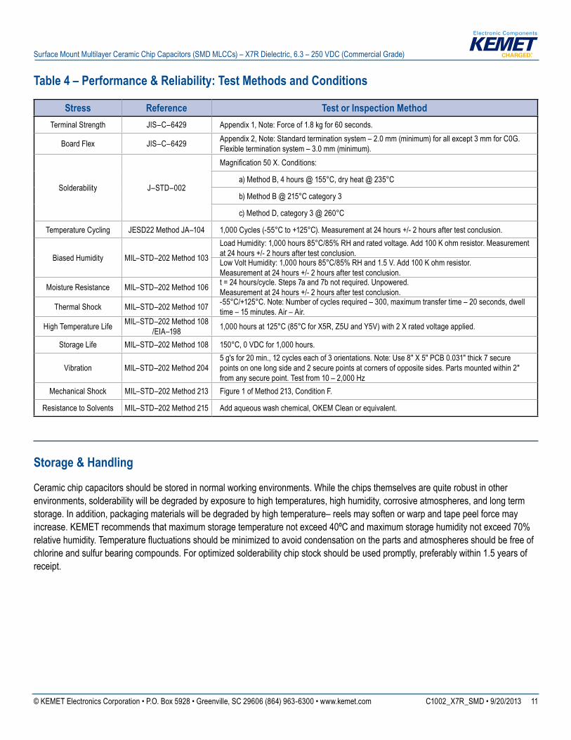
Table 4 – Performance & Reliability: Test Methods and Conditions
Stress Reference Test or Inspection MethodTerminalStrength JIS–C–6429 Appendix1,Note:Forceof1.8kgfor60seconds.
Board Flex JIS–C–6429 Appendix2,Note:Standardterminationsystem–2.0mm(minimum)forallexcept3mmforC0G.Flexible termination system – 3.0 mm (minimum).
Solderability J–STD–002
Magnification50X.Conditions:
a)MethodB,4hours@155°C,dryheat@235°C
b)MethodB@215°Ccategory3
c)MethodD,category3@260°C
Temperature Cycling JESD22MethodJA–104 1,000Cycles(-55°Cto+125°C).Measurementat24hours+/-2hoursaftertestconclusion.
Biased Humidity MIL–STD–202Method103
LoadHumidity:1,000hours85°C/85%RHandratedvoltage.Add100Kohmresistor.Measurementat24hours+/-2hoursaftertestconclusion.LowVoltHumidity:1,000hours85°C/85%RHand1.5V.Add100Kohmresistor.Measurementat24hours+/-2hoursaftertestconclusion.
Moisture Resistance MIL–STD–202Method106 t=24hours/cycle.Steps7aand7bnotrequired.Unpowered.Measurementat24hours+/-2hoursaftertestconclusion.
ThermalShock MIL–STD–202Method107 -55°C/+125°C.Note:Numberofcyclesrequired–300,maximumtransfertime–20seconds,dwelltime – 15 minutes. Air – Air.
HighTemperatureLife MIL–STD–202Method108/EIA–198 1,000hoursat125°C(85°CforX5R,Z5UandY5V)with2Xratedvoltageapplied.
StorageLife MIL–STD–202Method108 150°C,0VDCfor1,000hours.
Vibration MIL–STD–202Method2045g'sfor20min.,12cycleseachof3orientations.Note:Use8"X5"PCB0.031"thick7securepointsononelongsideand2securepointsatcornersofoppositesides.Partsmountedwithin2"from any secure point. Test from 10 – 2,000 Hz
MechanicalShock MIL–STD–202Method213 Figure1ofMethod213,ConditionF.
Resistance to Solvents MIL–STD–202Method215 Addaqueouswashchemical,OKEMCleanorequivalent.
Storage & Handling
Ceramicchipcapacitorsshouldbestoredinnormalworkingenvironments.Whilethechipsthemselvesarequiterobustinotherenvironments,solderabilitywillbedegradedbyexposuretohightemperatures,highhumidity,corrosiveatmospheres,andlongtermstorage.Inaddition,packagingmaterialswillbedegradedbyhightemperature–reelsmaysoftenorwarpandtapepeelforcemayincrease.KEMETrecommendsthatmaximumstoragetemperaturenotexceed40ºCandmaximumstoragehumiditynotexceed70%relativehumidity.Temperaturefluctuationsshouldbeminimizedtoavoidcondensationonthepartsandatmospheresshouldbefreeofchlorineandsulfurbearingcompounds.Foroptimizedsolderabilitychipstockshouldbeusedpromptly,preferablywithin1.5yearsofreceipt.
© KEMET Electronics Corporation • P.O. Box 5928 • Greenville, SC 29606 (864) 963-6300 • www.kemet.com C1002_X7R_SMD • 9/20/2013 12
Surface Mount Multilayer Ceramic Chip Capacitors (SMD MLCCs) – X7R Dielectric, 6.3 – 250 VDC (Commercial Grade)
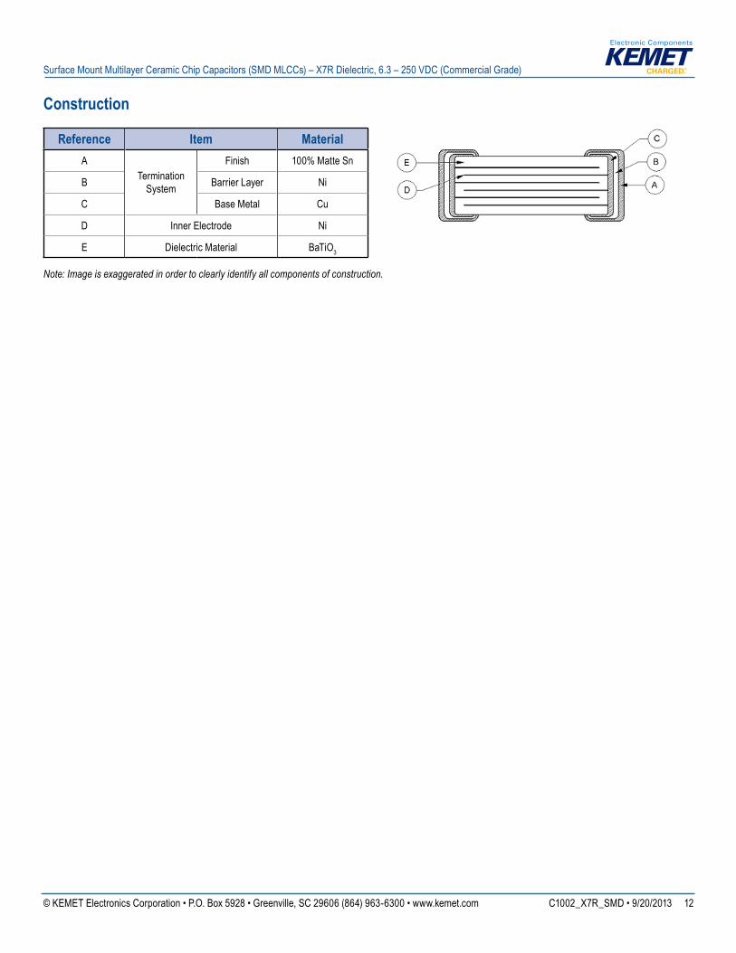
Construction
Reference Item MaterialA
Termination System
Finish 100% Matte Sn
B BarrierLayer Ni
C Base Metal Cu
D Inner Electrode Ni
E Dielectric Material BaTiO3
Note: Image is exaggerated in order to clearly identify all components of construction.
© KEMET Electronics Corporation • P.O. Box 5928 • Greenville, SC 29606 (864) 963-6300 • www.kemet.com C1002_X7R_SMD • 9/20/2013 13
Surface Mount Multilayer Ceramic Chip Capacitors (SMD MLCCs) – X7R Dielectric, 6.3 – 250 VDC (Commercial Grade)
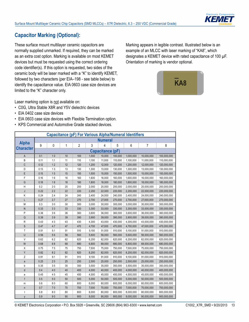
Capacitor Marking (Optional):Thesesurfacemountmultilayerceramiccapacitorsarenormallysuppliedunmarked.Ifrequired,theycanbemarkedas an extra cost option. Marking is available on most KEMET devicesbutmustberequestedusingthecorrectorderingcodeidentifier(s).Ifthisoptionisrequested,twosidesoftheceramicbodywillbelasermarkedwitha“K”toidentifyKEMET,followedbytwocharacters(perEIA–198-seetablebelow)toidentifythecapacitancevalue.EIA0603casesizedevicesarelimitedtothe“K”characteronly.
Lasermarkingoptionisnotavailableon:• C0G,UltraStableX8RandY5Vdielectricdevices• EIA 0402 case size devices • EIA0603casesizedeviceswithFlexibleTerminationoption.• KPS Commercial and Automotive Grade stacked devices.
Marking appears in legible contrast. Illustrated below is an exampleofanMLCCwithlasermarkingof“KA8”,whichdesignatesaKEMETdevicewithratedcapacitanceof100µF.Orientation of marking is vendor optional.
_KA8
Capacitance (pF) For Various Alpha/Numeral Identifi ers
AlphaCharacter
Numeral9 0 1 2 3 4 5 6 7 8
Capacitance (pF)A 0.1 1 0 10 100 1,000 10,000 100,000 1,000,000 10,000,000 100,000,000B 0.11 1.1 11 110 1,100 11,000 110,000 1,100,000 11,000,000 110,000,000C 0.12 1 2 12 120 1,200 12,000 120,000 1,200,000 12,000,000 120,000,000D 0.13 1 3 13 130 1,300 13,000 130,000 1,300,000 13,000,000 130,000,000E 0.15 1 5 15 150 1,500 15,000 150,000 1,500,000 15,000,000 150,000,000F 0.16 1 6 16 160 1,600 16,000 160,000 1,600,000 16,000,000 160,000,000G 0.18 1 8 18 180 1,800 18,000 180,000 1,800,000 18,000,000 180,000,000H 0.2 2 0 20 200 2,000 20,000 200,000 2,000,000 20,000,000 200,000,000J 0.22 2 2 22 220 2,200 22,000 220,000 2,200,000 22,000,000 220,000,000K 0.24 2.4 24 240 2,400 24,000 240,000 2,400,000 24,000,000 240,000,000L 0.27 2.7 27 270 2,700 27,000 270,000 2,700,000 27,000,000 270,000,000M 0.3 3 0 30 300 3,000 30,000 300,000 3,000,000 30,000,000 300,000,000N 0.33 3 3 33 330 3,300 33,000 330,000 3,300,000 33,000,000 330,000,000P 0.36 3 6 36 360 3,600 36,000 360,000 3,600,000 36,000,000 360,000,000Q 0.39 3 9 39 390 3,900 39,000 390,000 3,900,000 39,000,000 390,000,000R 0.43 4 3 43 430 4,300 43,000 430,000 4,300,000 43,000,000 430,000,000S 0.47 4.7 47 470 4,700 47,000 470,000 4,700,000 47,000,000 470,000,000T 0.51 5.1 51 510 5,100 51,000 510,000 5,100,000 51,000,000 510,000,000U 0.56 5 6 56 560 5,600 56,000 560,000 5,600,000 56,000,000 560,000,000V 0.62 6 2 62 620 6,200 62,000 620,000 6,200,000 62,000,000 620,000,000W 0.68 6 8 68 680 6,800 68,000 680,000 6,800,000 68,000,000 680,000,000X 0.75 7 5 75 750 7,500 75,000 750,000 7,500,000 75,000,000 750,000,000Y 0.82 8 2 82 820 8,200 82,000 820,000 8,200,000 82,000,000 820,000,000Z 0.91 9.1 91 910 9,100 91,000 910,000 9,100,000 91,000,000 910,000,000a 0.25 2 5 25 250 2,500 25,000 250,000 2,500,000 25,000,000 250,000,000b 0.35 3 5 35 350 3,500 35,000 350,000 3,500,000 35,000,000 350,000,000d 0.4 4 0 40 400 4,000 40,000 400,000 4,000,000 40,000,000 400,000,000e 0.45 4 5 45 450 4,500 45,000 450,000 4,500,000 45,000,000 450,000,000f 0.5 5 0 50 500 5,000 50,000 500,000 5,000,000 50,000,000 500,000,000m 0.6 6 0 60 600 6,000 60,000 600,000 6,000,000 60,000,000 600,000,000n 0.7 7 0 70 700 7,000 70,000 700,000 7,000,000 70,000,000 700,000,000t 0.8 8 0 80 800 8,000 80,000 800,000 8,000,000 80,000,000 800,000,000y 0.9 9 0 90 900 9,000 90,000 900,000 9,000,000 90,000,000 900,000,000
© KEMET Electronics Corporation • P.O. Box 5928 • Greenville, SC 29606 (864) 963-6300 • www.kemet.com C1002_X7R_SMD • 9/20/2013 14
Surface Mount Multilayer Ceramic Chip Capacitors (SMD MLCCs) – X7R Dielectric, 6.3 – 250 VDC (Commercial Grade)
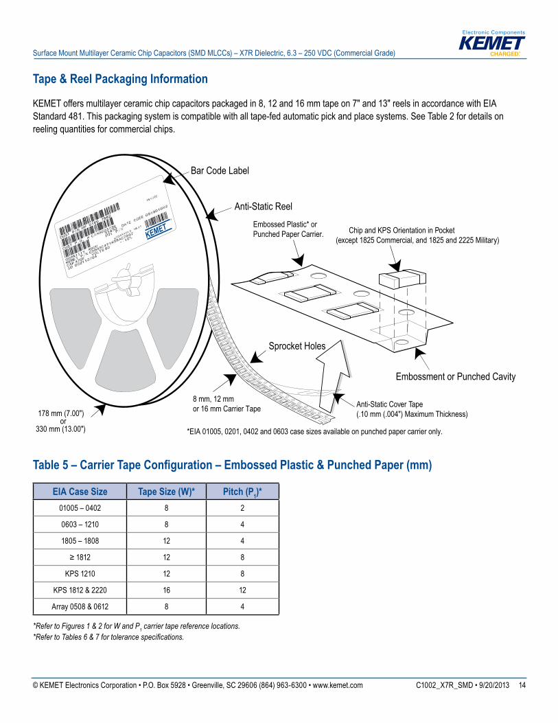
Tape & Reel Packaging Information
KEMEToffersmultilayerceramicchipcapacitorspackagedin8,12and16mmtapeon7"and13"reelsinaccordancewithEIAStandard481.Thispackagingsystemiscompatiblewithalltape-fedautomaticpickandplacesystems.SeeTable2fordetailsonreelingquantitiesforcommercialchips.
8 mm, 12 mmor 16 mm Carrier Tape 178 mm (7.00")
or330 mm (13.00")
Anti-Static ReelEmbossed Plastic* or Punched Paper Carrier.
Embossment or Punched Cavity
Anti-Static Cover Tape(.10 mm (.004") Maximum Thickness)
Chip and KPS Orientation in Pocket(except 1825 Commercial, and 1825 and 2225 Military)
*EIA 01005, 0201, 0402 and 0603 case sizes available on punched paper carrier only.
KEMET®
Bar Code Label
Sprocket Holes
Table 5 – Carrier Tape Confi guration – Embossed Plastic & Punched Paper (mm)
EIA Case Size Tape Size (W)* Pitch (P1)*01005 – 0402 8 2
0603 – 1210 8 4
1805 – 1808 12 4
≥1812 12 8
KPS 1210 12 8
KPS 1812 & 2220 16 12
Array 0508 & 0612 8 4
*Refer to Figures 1 & 2 for W and P1 carrier tape reference locations.*Refer to Tables 6 & 7 for tolerance specifi cations.
© KEMET Electronics Corporation • P.O. Box 5928 • Greenville, SC 29606 (864) 963-6300 • www.kemet.com C1002_X7R_SMD • 9/20/2013 15
Surface Mount Multilayer Ceramic Chip Capacitors (SMD MLCCs) – X7R Dielectric, 6.3 – 250 VDC (Commercial Grade)
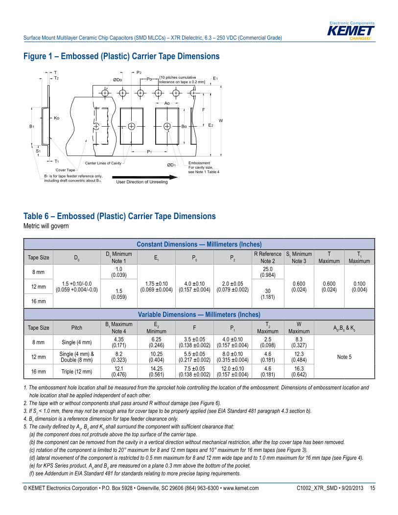
Figure 1 – Embossed (Plastic) Carrier Tape Dimensions
PoT
F
W
Center Lines of Cavity
Ao
Bo
User Direction of Unreeling
Cover Tape
Ko
B1 is for tape feeder reference only, including draft concentric about B o.
T2
ØD1
ØDo
B1
S1
T1
E1
E2
P1
P2
EmbossmentFor cavity size,see Note 1 Table 4
[10 pitches cumulativetolerance on tape ± 0.2 mm]
Table 6 – Embossed (Plastic) Carrier Tape DimensionsMetric will govern
Constant Dimensions — Millimeters (Inches)
Tape Size D0 D1 Minimum
Note 1 E1 P0 P2 R Reference
Note 2S1 Minimum
Note 3T
MaximumT1
Maximum
8 mm
1.5 +0.10/-0.0 (0.059 +0.004/-0.0)
1.0 (0.039)
1.75 ±0.10 (0.069 ±0.004)
4.0 ±0.10 (0.157 ±0.004)
2.0 ±0.05(0.079 ±0.002)
25.0 (0.984)
0.600 (0.024)
0.600 (0.024)
0.100 (0.004)12 mm
1.5 (0.059)
30 (1.181)
16 mm
Variable Dimensions — Millimeters (Inches)
Tape Size Pitch B1 MaximumNote 4
E2 Minimum F P1
T2 Maximum
WMaximum A0,B0 & K0
8 mm Single (4 mm) 4.35 (0.171)
6.25 (0.246)
3.5 ±0.05 (0.138 ±0.002)
4.0 ±0.10(0.157 ±0.004)
2.5 (0.098)
8.3 (0.327)
Note 512 mm Single (4 mm) & Double (8 mm)
8.2 (0.323)
10.25 (0.404)
5.5 ±0.05 (0.217 ±0.002)
8.0 ±0.10(0.315 ±0.004)
4.6 (0.181)
12.3 (0.484)
16 mm Triple (12 mm) 12.1 (0.476)
14.25(0.561)
7.5 ±0.05(0.138 ±0.002)
12.0 ±0.10(0.157 ±0.004)
4.6 (0.181)
16.3 (0.642)
1. The embossment hole location shall be measured from the sprocket hole controlling the location of the embossment. Dimensions of embossment location and hole location shall be applied independent of each other.
2. The tape with or without components shall pass around R without damage (see Figure 6).3. If S1 < 1.0 mm, there may not be enough area for cover tape to be properly applied (see EIA Standard 481 paragraph 4.3 section b).4. B1 dimension is a reference dimension for tape feeder clearance only.5. The cavity defi ned by A0, B0 and K0 shall surround the component with suffi cient clearance that: (a) the component does not protrude above the top surface of the carrier tape. (b) the component can be removed from the cavity in a vertical direction without mechanical restriction, after the top cover tape has been removed. (c) rotation of the component is limited to 20° maximum for 8 and 12 mm tapes and 10° maximum for 16 mm tapes (see Figure 3). (d) lateral movement of the component is restricted to 0.5 mm maximum for 8 and 12 mm wide tape and to 1.0 mm maximum for 16 mm tape (see Figure 4). (e) for KPS Series product, A0 and B0 are measured on a plane 0.3 mm above the bottom of the pocket. (f) see Addendum in EIA Standard 481 for standards relating to more precise taping requirements.
© KEMET Electronics Corporation • P.O. Box 5928 • Greenville, SC 29606 (864) 963-6300 • www.kemet.com C1002_X7R_SMD • 9/20/2013 16
Surface Mount Multilayer Ceramic Chip Capacitors (SMD MLCCs) – X7R Dielectric, 6.3 – 250 VDC (Commercial Grade)
Figure 2 – Punched (Paper) Carrier Tape Dimensions
User Direction of Unreeling
Top Cover Tape
T
Center Lines of Cavity
P1
ØDo PoP2
E1
F
E2W
G
A0
B0
Cavity Size,SeeNote 1, Table 7
Bottom Cover Tape
T1
T1
Bottom Cover Tape
[10 pitches cumulativetolerance on tape ± 0.2 mm]
Table 7 – Punched (Paper) Carrier Tape Dimensions Metric will govern
Constant Dimensions — Millimeters (Inches)Tape Size D0 E1 P0 P2 T1 Maximum G Minimum R Reference
Note 2
8 mm 1.5 +0.10 -0.0 (0.059 +0.004 -0.0)
1.75 ±0.10 (0.069 ±0.004)
4.0 ±0.10 (0.157 ±0.004)
2.0 ±0.05 (0.079 ±0.002)
0.10 (0.004) Maximum
0.75 (0.030)
25 (0.984)
Variable Dimensions — Millimeters (Inches)Tape Size Pitch E2 Minimum F P1 T Maximum WMaximum A0 B0
8 mm Half (2 mm) 6.25 (0.246)
3.5 ±0.05 (0.138 ±0.002)
2.0 ±0.05 (0.079 ±0.002) 1.1
(0.098)
8.3(0.327) Note 1
8 mm Single (4 mm) 4.0 ±0.10 (0.157 ±0.004)
8.3(0.327)
1. The cavity defi ned by A0, B0 and T shall surround the component with suffi cient clearance that: a) the component does not protrude beyond either surface of the carrier tape. b) the component can be removed from the cavity in a vertical direction without mechanical restriction, after the top cover tape has been removed. c) rotation of the component is limited to 20° maximum (see Figure 3). d) lateral movement of the component is restricted to 0.5 mm maximum (see Figure 4). e) see Addendum in EIA Standard 481 for standards relating to more precise taping requirements.2. The tape with or without components shall pass around R without damage (see Figure 6).
© KEMET Electronics Corporation • P.O. Box 5928 • Greenville, SC 29606 (864) 963-6300 • www.kemet.com C1002_X7R_SMD • 9/20/2013 17
Surface Mount Multilayer Ceramic Chip Capacitors (SMD MLCCs) – X7R Dielectric, 6.3 – 250 VDC (Commercial Grade)
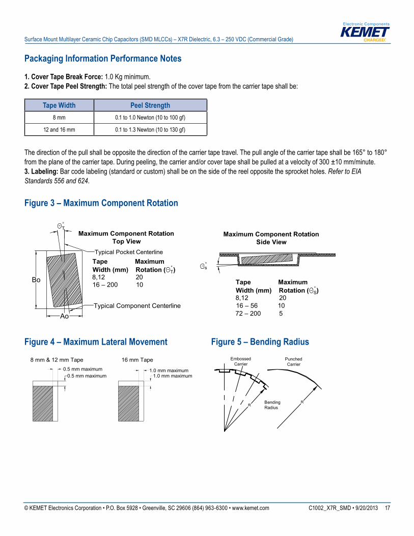
Packaging Information Performance Notes
1. Cover Tape Break Force: 1.0 Kg minimum.2. Cover Tape Peel Strength: Thetotalpeelstrengthofthecovertapefromthecarriertapeshallbe:
Tape Width Peel Strength8 mm 0.1 to 1.0 Newton (10 to 100 gf)
12 and 16 mm 0.1 to 1.3 Newton (10 to 130 gf)
Thedirectionofthepullshallbeoppositethedirectionofthecarriertapetravel.Thepullangleofthecarriertapeshallbe165°to180°fromtheplaneofthecarriertape.Duringpeeling,thecarrierand/orcovertapeshallbepulledatavelocityof300±10mm/minute.3. Labeling:Barcodelabeling(standardorcustom)shallbeonthesideofthereeloppositethesprocketholes.Refer to EIA Standards 556 and 624.
Figure 3 – Maximum Component Rotation
Ao
Bo
°T
°s
Maximum Component RotationTop View
Maximum Component RotationSide View
Tape MaximumWidth (mm) Rotation ( °
T)8,12 20 16 – 200 10 Tape Maximum
Width (mm) Rotation ( °S)
8,12 20 16 – 56 1072 – 200 5
Typical Pocket Centerline
Typical Component Centerline
Figure 4 – Maximum Lateral Movement
0.5 mm maximum0.5 mm maximum
8 mm & 12 mm Tape
1.0 mm maximum1.0 mm maximum
16 mm Tape
Figure 5 – Bending Radius
RRBending
Radius
EmbossedCarrier
PunchedCarrier
© KEMET Electronics Corporation • P.O. Box 5928 • Greenville, SC 29606 (864) 963-6300 • www.kemet.com C1002_X7R_SMD • 9/20/2013 18
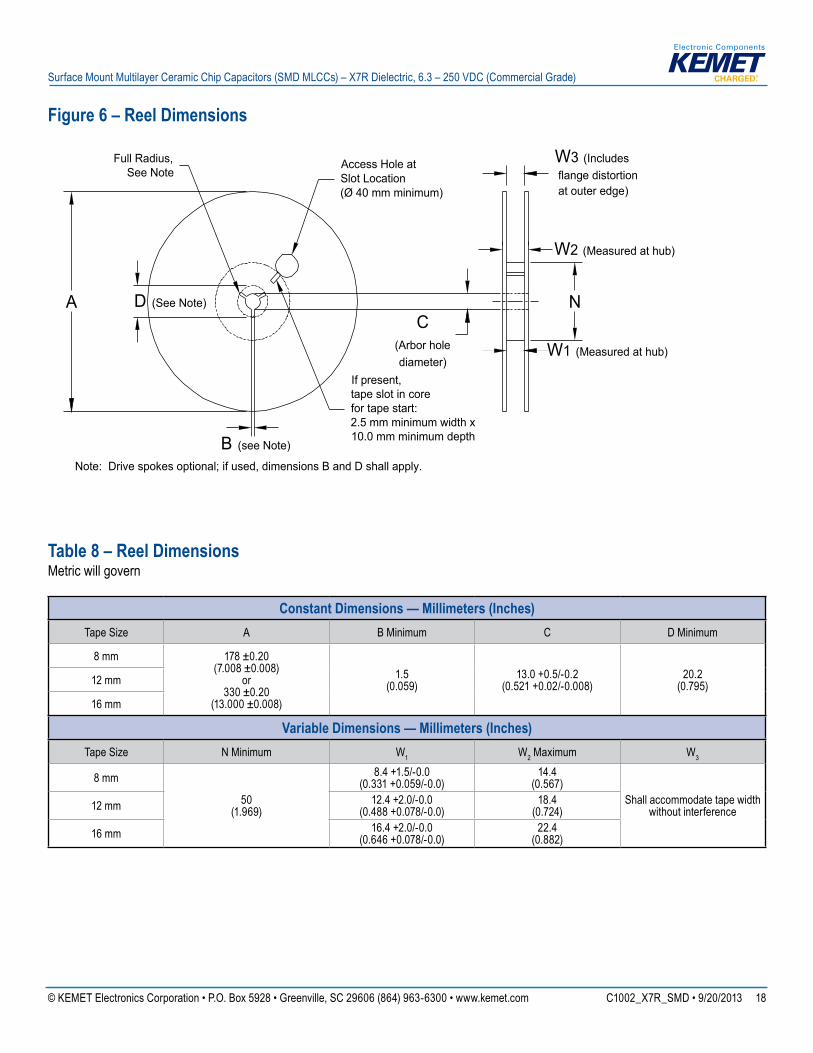
Surface Mount Multilayer Ceramic Chip Capacitors (SMD MLCCs) – X7R Dielectric, 6.3 – 250 VDC (Commercial Grade)
Figure 6 – Reel Dimensions
A D (See Note)
Full Radius,See Note
B (see Note)
Access Hole atSlot Location(Ø 40 mm minimum)
If present,tape slot in corefor tape start:2.5 mm minimum width x10.0 mm minimum depth
W3 (Includes flange distortion at outer edge)
W2 (Measured at hub)
W1 (Measured at hub)
C(Arbor holediameter)
Note: Drive spokes optional; if used, dimensions B and D shall apply.
N
Table 8 – Reel DimensionsMetric will govern
Constant Dimensions — Millimeters (Inches) Tape Size A B Minimum C D Minimum
8 mm 178 ±0.20 (7.008 ±0.008)
or330 ±0.20
(13.000 ±0.008)
1.5 (0.059)
13.0 +0.5/-0.2 (0.521 +0.02/-0.008)
20.2 (0.795)12 mm
16 mm
Variable Dimensions — Millimeters (Inches) Tape Size N Minimum W1 W2 Maximum W3
8 mm
50 (1.969)
8.4 +1.5/-0.0(0.331 +0.059/-0.0)
14.4 (0.567)
Shallaccommodatetapewidthwithoutinterference12 mm 12.4 +2.0/-0.0
(0.488 +0.078/-0.0) 18.4
(0.724)
16 mm 16.4 +2.0/-0.0(0.646 +0.078/-0.0)
22.4 (0.882)
© KEMET Electronics Corporation • P.O. Box 5928 • Greenville, SC 29606 (864) 963-6300 • www.kemet.com C1002_X7R_SMD • 9/20/2013 19
Surface Mount Multilayer Ceramic Chip Capacitors (SMD MLCCs) – X7R Dielectric, 6.3 – 250 VDC (Commercial Grade)
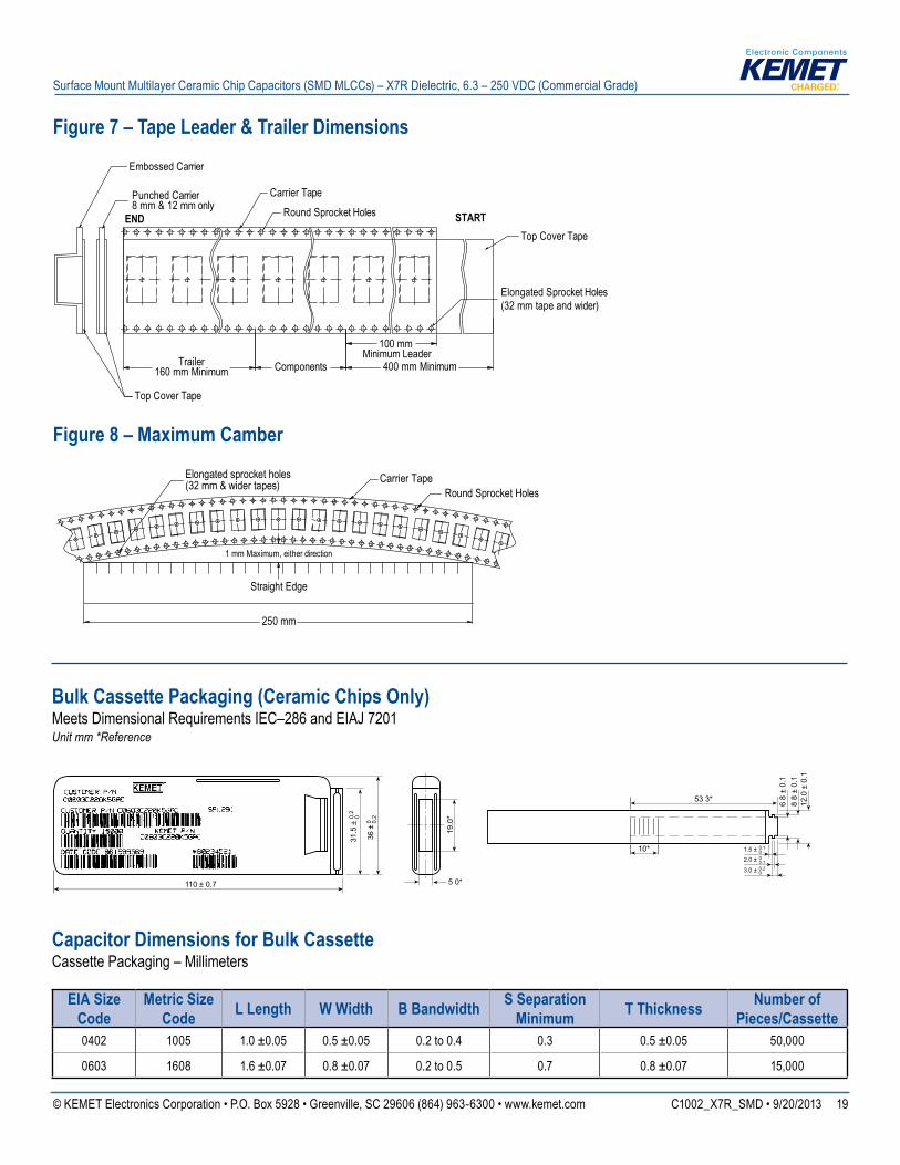
Figure 7 – Tape Leader & Trailer Dimensions
Trailer160 mm Minimum
Carrier Tape
END STARTRound Sprocket Holes
Elongated Sprocket Holes(32 mm tape and wider)
Top Cover Tape
Top Cover Tape
Punched Carrier8 mm & 12 mm only
Embossed Carrier
Components
100 mm Minimum Leader
400 mm Minimum
Figure 8 – Maximum Camber
Carrier TapeRound Sprocket Holes
1 mm Maximum, either direction
Straight Edge
250 mm
Elongated sprocket holes(32 mm & wider tapes)
Bulk Cassette Packaging (Ceramic Chips Only)MeetsDimensionalRequirementsIEC–286andEIAJ7201Unit mm *Reference
110 ± 0.7
31.5
± 00.
2
36 ±
0 0.2
19.0
*
5 0*
10*
53 3* 68
± 0.
18
8 ±
0.1
12.0
± 0
.1
3.0 ± 00.2
2.0 ± 0.10
1.5 ± 00.1
Capacitor Dimensions for Bulk CassetteCassette Packaging – Millimeters
EIA Size Code
Metric Size Code L Length W Width B Bandwidth S Separation
Minimum T Thickness Number of Pieces/Cassette
0402 1005 1.0 ±0.05 0.5 ±0.05 0.2 to 0.4 0.3 0.5 ±0.05 50,000
0603 1608 1.6 ±0.07 0.8 ±0.07 0.2 to 0.5 0.7 0.8 ±0.07 15,000
© KEMET Electronics Corporation • P.O. Box 5928 • Greenville, SC 29606 (864) 963-6300 • www.kemet.com C1002_X7R_SMD • 9/20/2013 20
Surface Mount Multilayer Ceramic Chip Capacitors (SMD MLCCs) – X7R Dielectric, 6.3 – 250 VDC (Commercial Grade)
KEMET Corporation World Headquarters
2835KEMETWaySimpsonville, SC 29681
MailingAddress:P.O. Box 5928 Greenville, SC 29606
www.kemet.com Tel:864-963-6300Fax:864-963-6521
Corporate Offi cesFortLauderdale,FLTel:954-766-2800
North America
SoutheastLakeMary,FLTel:407-855-8886
NortheastWilmington,MATel:978-658-1663
CentralNovi, MITel:248-994-1030
WestMilpitas, CATel:408-433-9950
Mexico Guadalajara, Jalisco Tel:52-33-3123-2141
Europe
Southern EuropeParis, FranceTel:33-1-4646-1006
Sasso Marconi, ItalyTel:39-051-939111
Central EuropeLandsberg,GermanyTel:49-8191-3350800
Kamen, GermanyTel:49-2307-438110
Northern EuropeBishop’sStortford,UnitedKingdomTel:44-1279-460122
Espoo, FinlandTel:358-9-5406-5000
Asia
Northeast AsiaHong KongTel:852-2305-1168
Shenzhen,ChinaTel:86-755-2518-1306
Beijing,ChinaTel:86-10-5829-1711
Shanghai,ChinaTel:86-21-6447-0707
Taipei, TaiwanTel:886-2-27528585
Southeast AsiaSingaporeTel:65-6586-1900
Penang, MalaysiaTel:60-4-6430200
Bangalore, IndiaTel:91-806-53-76817
Note: KEMET reserves the right to modify minor details of internal and external construction at any time in the interest of product improvement. KEMET does not assume any responsibility for infringement that might result from the use of KEMET Capacitors in potential circuit designs. KEMET is a registered trademark of KEMET Electronics Corporation.
© KEMET Electronics Corporation • P.O. Box 5928 • Greenville, SC 29606 (864) 963-6300 • www.kemet.com C1002_X7R_SMD • 9/20/2013 21
Surface Mount Multilayer Ceramic Chip Capacitors (SMD MLCCs) – X7R Dielectric, 6.3 – 250 VDC (Commercial Grade)
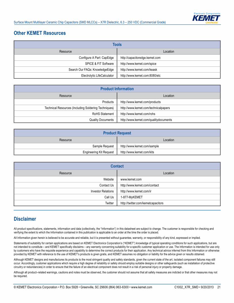
Other KEMET Resources
ToolsResource Location
ConfigureAPart:CapEdge http://capacitoredge.kemet.comSPICE & FIT Software http://www.kemet.com/spice
SearchOurFAQs:KnowledgeEdge http://www.kemet.com/keaskElectrolyticLifeCalculator http://www.kemet.com:8080/elc
Product InformationResource Location
Products http://www.kemet.com/productsTechnicalResources(IncludingSolderingTechniques) http://www.kemet.com/technicalpapers
RoHS Statement http://www.kemet.com/rohsQualityDocuments http://www.kemet.com/qualitydocuments
Product RequestResource Location
SampleRequest http://www.kemet.com/sampleEngineeringKitRequest http://www.kemet.com/kits
ContactResource Location
Website www.kemet.comContact Us http://www.kemet.com/contact
Investor Relations http://www.kemet.com/irCall Us 1-877-MyKEMETTwitter http://twitter.com/kemetcapacitors
DisclaimerAllproductspecifications,statements,informationanddata(collectively,the“Information”)inthisdatasheetaresubjecttochange.ThecustomerisresponsibleforcheckingandverifyingtheextenttowhichtheInformationcontainedinthispublicationisapplicabletoanorderatthetimetheorderisplaced.
AllInformationgivenhereinisbelievedtobeaccurateandreliable,butitispresentedwithoutguarantee,warranty,orresponsibilityofanykind,expressedorimplied.
StatementsofsuitabilityforcertainapplicationsarebasedonKEMETElectronicsCorporation’s(“KEMET”)knowledgeoftypicaloperatingconditionsforsuchapplications,butarenotintendedtoconstitute–andKEMETspecificallydisclaims–anywarrantyconcerningsuitabilityforaspecificcustomerapplicationoruse.TheInformationisintendedforuseonlybycustomerswhohavetherequisiteexperienceandcapabilitytodeterminethecorrectproductsfortheirapplication.AnytechnicaladviceinferredfromthisInformationorotherwiseprovidedbyKEMETwithreferencetotheuseofKEMET’sproductsisgivengratis,andKEMETassumesnoobligationorliabilityfortheadvicegivenorresultsobtained.
AlthoughKEMETdesignsandmanufacturesitsproductstothemoststringentqualityandsafetystandards,giventhecurrentstateoftheart,isolatedcomponentfailuresmaystilloccur.Accordingly,customerapplicationswhichrequireahighdegreeofreliabilityorsafetyshouldemploysuitabledesignsorothersafeguards(suchasinstallationofprotectivecircuitryorredundancies)inordertoensurethatthefailureofanelectricalcomponentdoesnotresultinariskofpersonalinjuryorpropertydamage.
Althoughallproduct–relatedwarnings,cautionsandnotesmustbeobserved,thecustomershouldnotassumethatallsafetymeasuresareindictedorthatothermeasuresmaynotberequired.
© KEMET Electronics Corporation • P.O. Box 5928 • Greenville, SC 29606 (864) 963-6300 • www.kemet.com C1002_X7R_SMD • 9/20/2013 22
Surface Mount Multilayer Ceramic Chip Capacitors (SMD MLCCs) – X7R Dielectric, 6.3 – 250 VDC (Commercial Grade)
Related Documents


