SEMI-ANNUAL STATUS REPORT III on The Influence of Polarization on Millimeter Wave Propagation through Rain C. W. BOSTIAN, W. L. STUTZMAN, PARIS H. WILEY and R. E. MARSHALL Submitted To: National Aeronautics and Space Administration Washington, D. C. NASA GRANT NUMBER NGR.47-004-091 Covering the Period i January j 1 -June 30, 1973 Juiy11973 Electrical Engineering Department Virginia Polytechnic Institute and State University Blacksburg,, Virginia 24061 https://ntrs.nasa.gov/search.jsp?R=19740002029 2018-06-29T01:07:37+00:00Z

Welcome message from author
This document is posted to help you gain knowledge. Please leave a comment to let me know what you think about it! Share it to your friends and learn new things together.
Transcript

SEMI-ANNUAL STATUS REPORT III
on
The Influence of Polarization on
Millimeter Wave Propagation through Rain
C. W. BOSTIAN, W. L. STUTZMAN,PARIS H. WILEY and R. E. MARSHALL
Submitted To: National Aeronautics and Space Administration
Washington, D. C.
NASA GRANT NUMBER NGR.47-004-091
Covering the Period i January j 1 - June 30, 1973
J u i y 1 1 9 7 3
Electrical Engineering Department
Virginia Polytechnic Institute and State University
Blacksburg,, Virginia 24061
https://ntrs.nasa.gov/search.jsp?R=19740002029 2018-06-29T01:07:37+00:00Z

PROJECT PERSONNEL
Dr. Charles W. Bostian, Principal Investigator
Dr. Warren L. Stutzman, Co-Principal Investigator
Dr. Paris H. Wiley, Faculty Associate
Mr. Robert E. Marshall, Graduate Research Assistant

TABLE OF CONTENTS
Page
1. Introduction 1
2. Narrative Summary of the Report Period 2
3. Theoretical Investigation 4
4. Data Processing 8
5. Data Presentation and Analysis 12
6. Literature Cited 90
7. Appendix: Considerations in RF System Design
for Cross Polarization Measurements 91

1. Introduction
This report describes the third six months of a continuing program
for the measurement and analysis of the depolarization and attenuation
that occur when millimeter wave radio signals propagate through rain.
Technical details covered in previous reports are repeated only as
necessary for clarity.
During the reporting period, progress was made in three major areas:
the processing of recorded 1972 data, acquisition and processing of a
large amount of 1973 data, and the development of a new theoretical
model to predict rain cross polarization and attenuation. Following
a brief narrative summary of the report period, each of these topics
will be described in more detail.
2. Narrative Summary of the Report Period
2.1 January
During January the primary concern was to develop an improved
theoretical model for rain depolarization. An effort to represent
rain scatter by Stevenson's 1953 low-frequency expansion for plane
wave scattering by a lossy oblate spheroid was abandoned when it
became apparent that Stevenson's approach would not converge fori
high permittivity scatterers like raindrops. Work continued on what
was to become a new depolarization model based on Oguchi's 1973 single
raindrop scattering functions.
2.2 February
The basic scattering model for depolarization prediction was
completed this month.

An effort was made to achieve optimum antenna alignment prior to
the 1973 thunderstorm season. Last year maximum cross polarization
isolation had occurred simultaneously on both channels, but now when
the isolation of one channel was maximized the isolation on the other
was not. Apparently one antenna is slightly out of adjustment and itsi
polarizations are not quite orthogonal (perhaps 89° apart instead of
90°) . The manufacturer could offer no suggestions beyond a trial-and-
error attempt at correction. As an interim solution the antennas were
aligned so that the residual + to - and - to + cross polarization levels
were about 25 dB and 50 dB respectively. Since our main interest is
in high rain rate data, this was an acceptable interim solution.
2.3 March
The data processing computer programs were modified to calculate
both the average cross polarization levels at each integer rain rate
and the standard deviation of the cross polarization data contributingi
to each average value. Subroutines were written to draw error bars
showing + and - one standard deviation on computer plots of average
cross polarization level versus rainfall rate. Computer routines were
developed to.extract attenuation values from recorded data and to
generate scatter plots of attenuation versus rain rates as well as
plots of average attenuation with error bars. A subroutine was written
to display average attenuation for each integer rain rate versus
average cross polarization-level for the same rain rate value. All
of these programs were used to generate the data presented in later
sections of this report.
Intense rainstorms were observed on March 16 and 17.

2.4 April
A new local oscillator (LO) for the receiver arrived and was
installed. Although initially unstable in frequency, it stabilizedi
after about a week's operation and remained stable for the rest of
April and May.
A storm occured on April 4.
2.5 May
The receiver calibration was checked on May 17 and found to be
unchanged.
An inspection of the raingauge network indicated that all gauges
but one were in good repair and working properly. The outer housing
of gauge //5 was replaced because of flaking paint.
Preparatory to setting up an on-line phase measuring system later
this year, a vector voltmeter was connected between the IF output ports
on the two receiver channels. With the instrument adjusted to read
0° phase difference between the incoming + channel and - channel co-
polarized signals, phase differences of 120° were measured between
the + channel direct signal and the - channel cross polarized signal
and 160° between the - channel direct signal and the + channel cross
polarized signal. In each case, the cross polarized signal was leading
the copolarized signal. These phase differences remained constant
over an observing period of about 10 minutes. While their absolute
values-are indicative only-of-slight component differences between
the two channels, the stability of the clear weather phase differences
indicates that measurements of rain-induced changes in differential
phase shift can be made.

Storms occurred on May 23, 26, 27, and 28. The storm on May 28
produced a peak rainfall rate of 217.4 mm/hour on one gauge for one
time interval between trips.
2.6 June
On June 3 a plexiglass roof was installed over the receiving
antenna. This will reduce the amount of water collected on the re-
flecting surface and the feed. Sufficient data are not yet available
to indicate whether or not the roof reduces the data scatter at lowi .
rain rates.
Frequency drift in the receiver LO again became a problem. An
oven to keep the LO at a constant temperature was installed on June 14
in an effort to end the drift.
3. Theoretical. Investigation
3.1 Introduction
During this report period a new method for calculating rain de-
polarization was developed. Called the scattering method, it was
described in detail in Interim Report I of this project, and the
information contained there will not be repeated. The scattering
method provides a means for calculating rain depolarization and
attenuation that is independent both of van de Hulst's equivalent
refractive index (van de Hulst, 1957) and of the differential
Attenuation-differential phase shift method (Watson and Arbabi,
1973). Since the important rain parameters are explicit rather
than implicit, it provides a rapid means for analyzing propagation
through rain under arbitrary drop shape and size distribution.
3.2 Discussion of Theoretical Models
There are presently three models for predicting the cross polar-
ization level at a given rainfall rate. The differential attenuation
method developed by Thomas (1971) was used to generate theoretical
curves for Semi-Annual Status Reports I and I_I_ of this project. UsingI
Oguchi's 1964 differential attenuation coefficients for this and similar
experiments, it usually predicts lower cross polarization levels (i...e.
greater isolations) than are measured. Substitution of Oguchi's revised
(1973) coefficients into the Thomas model leads to predicted cross
polarization generally higher than those measured.
The values of Oguchi's 1973 coefficients have been confirmed
independently by Watson;(private communication); hence, the difference
between measured cross polarization levels and Thomas's predictions
seem to lie largely in Thomas's neglect of differential phase shifts
and in the prevalent assumption that all raindrops are oblate spheroids.
Watson and Arbabi (1973) have shown that differential attenuation and
differential phase shift are equally important in determining the
received cross polarization ratio, and if one takes phase shift into
account, calculated cross polarization levels are significantly dif-
ferent from the Thomas model. This effect is illustrated in Figure 1.
If one assumes 100% oblate drops, the scattering model and Watson's
differential attenuation-differential phase shift model predict essen-
tially equivalent cross polarization levels. Figure 2 compares the
two models for a 1 km path with +45° linear polarization and uncanted
drops. However, there is meteorological evidence that the proportioni
of oblate drops in real rain is actually about 40% (see Interim Report I)

•3
coco
0)-d
CO
IH
"84Jo0)rH000)c
8.8
8
-9
Bo:•as
z:z:
ey
8cr
uLDo:
U0UJBin
8-ui
O.Q
000 QQ01- 00 02- 00 OE- 00 O-- 00 CB'90 H3A3"! NOIlbZIfctnOd SSOdD

TTV
UJa:UJ
OCVJ
ino
IO
E
UJ
!5cr
50 <^ a:
If)
a)4-1COM
CO3co
0)
0)
cO
N•H
OaCOCOO
COCo
ro
CJ 4J•H CO-aCO 43
D. CO
COO
CUt-lOCO
CM
00•Hfe
J
(9P) 13A31 NOIiVZIHVlOd SSOHD

and the data collected by this project support the 40% figure. The
effect of a 40% proportion of oblate drops is shown in Figure 2. The
theoretical curves which appear in the data presentations to follow
have been drawn for a. raindrop population which is 40% oblate.
3.3 The Question of Phase Shift
Although the scattering model and the differential attenuation-
differential phase shift models predict essentially the same cross
polarization level for a given raindrop population, the scattering
model and the van de Hulst (1957) approach disagree as to the exact
dependence of phase shift on polarization. For example, Figure 3
shows the differential phase shift at 19.3 GHz for a one kilometer
path. In the figure, differential phase shift by which the phase of
the received signal for a vertically polarized transmitted wave leads
the phase of the received signal for a horizontally polarized trans-
mitted wave. Shown for comparison are results of the scattering model,
of Oguchi (1973), and of Morrison, et. al. (1973). Although there are
no experimental data to support any of these curves, some differential
phase measurements will be made during 1973.
4. Data Processing
4.1 Introduction
The principal data processing efforts during this report period
were directed toward (1) the calculation of standard deviations for
measured cross polarization data and the presentation of error bars
on computer plots of average cross polarization level versus rainfall
rate, (2) the development of programs to extract and display attenuation

oin
inCM
LJ
5cr.
•Hfi(0
01(0
p.
c01
N»H «.o o
w ^o o\•H <H
« IS•H «)
edo
lOCM
o0)
H
Q)Vi
00•H
MO
Oro
(•6ap)"jj|HS 3SWd

10
data, and (3) streamlining the data reduction program.
4.2 Standard Deviations and Error Bars
The basic data reduction approach (see Semi-Anriual Status Report II )
has been to generate 15-second running averages of all data and to plot
selected running averages at one-second intervals over the course of a
storm. This leads to a scatter plot of cross polarization level (or
some other signal parameter) versus rainfall rate. The average cross
polarization level for each integer rainfall rate can then be determined
by collecting all of the cross polarization values corresponding to rain
rates greater than or equal to the integer value but less than the next
highest integer rain rate and averaging them. Suppose we identify all
of the cross polarization data points associated with rain rates R such
that 1 <_ R < I -f 1 where I is an integer. Let there be N.(I) of these
points. We can identify each point as X(I,J), J = 1, N(I). The average
cross polarization level corresponding to an integer rain rate of I mm/hr
is then
J=l
and the standard deviation of the X(I,J) population is
J=lN(I) - 1
- This procedure was '"used to calculate standard deviations for the
data in Section 5. To keep core requirements within reasonable bounds,
N(I) was limited to a maximum value of 70. The plotting subroutines
were modified to draw error bars extending from < X(I) > - S(I) to

11
< X(J) > + S(I) on plots of < X(I) > versus rainfall rate.
4.3 Attenuation Calculation and Display
Rain attenuation is more difficult to measure than rain-induced
cross polarization because attenuation measurement requires a clear
weather reference signal that is precisely known and has the same value
before and after a storm. So long as the cross-polarized signal stays
above the receiver threshold, the measured cross polarization level is
independent of transmitter power, antenna gains, path loss, and the
receiver gain and hence unaffected by variations in these quantities.
Because the reference signal depends strongly on all of these things,
measured values of attenuation must be interpreted with this fact in
mind.
A further difficulty peculiar to this project is that measured
attenuation values tend to be small for the short path, i.e., about
.124 dB per mm/hr. This means that a one dB error in estimating the
clear weather reference signal can introduce a significant percentage
error into attenuation computations.
For calculating attenuation it was decided to use as a reference
a 30-second average of the received signal level centered 60 seconds
after the beginning of a storm. For most storms this was satisfactory,
but for the occasional storm that begins with a "step function" of
rain, the rain rate was significant before the PB-440 computer began
recording-received signal levels.-- This meant that the reference-signal
was too low and that some calculated attenuations would come out negative,
Since negative attenuation is non-physical (rain does not amplify) the
IBM 370 data processing program was Instructed to scan the attenuation

12
data array for each storm and, if it found negative values, to add the
proper constant to make the minimum attenuation zero.
5. Data Presentation and Analysis
5.1 1972 Data
5.1.1 Introduction
Semi-annual Status Report II presented scatter plots and average
plots of measured cross polarization level versus rainfall rate for
six 1972 storms. At that time, scattering model predictions were not
available for comparison with experiment and attenuation values had not
been extracted from the measured data. For these reasons data from the
important 1972 storms are included in this report. In all the figures
which follow a * indicates an average of all data from both channels
corresponding to an integer value of rain rate and a A indicates a
value predicted by the scattering model. On cross polarization plot
a | indicates + to - polarization conversion and - to + conversion is
shown as a +. For attenuation plots + channel attenuation is shown as
a + and - channel attenuation is shown as a |. In cases where separate
averages from both channels appear on the same graph, points indicated
by a | are displaced 0.03 inches to the right of their correct location
to separate them from the + points.
Usually 5 figures are presented for each 1972 storm. These are
(1) average cross polarization level versus rain fate for each channel,
(2) average cross polarization level versus rain rate with both channels
together, (3) average attenuation versus rain rate for each channel,
(4) average attenuation versus rain rate with both channels together,

13
and (5) average attenuation versus average cross polarization level with
rain rate as a parameter. The last eliminates measurement errors due
to rain inhomogeneity and is perhaps the best experimental test of the
scattering model.
5.1.2 August 4, 1972
During this storm only the + receiver channel was working. Figure 4
illustrates the average measured cross polarization level as a function
of rainfall rate. The attenuation values measured are not displayed
because they were essentially uncorrelated with rainfall rate and cross
polarization level. This is illustrated by Figure 5 which plots average
values of attenuation versus average cross polarization levels.
5.1.3 August 17, 1972
Figure 6 illustrates the average cross polarization level for each
channel measured during this storm. In Figure 7 both channels are com-
bined to yield a composite average. Figure 8 is a plot of average
attenuation versus rain rate for each channel and Figure 9 indicates
the average attenuation resulting when data from both channels are
together. Figure 10 displays average attenuation versus average cross
polarization level.
5.1.4 September 29, 1972
Figures 11 through 15 display data from this storm.
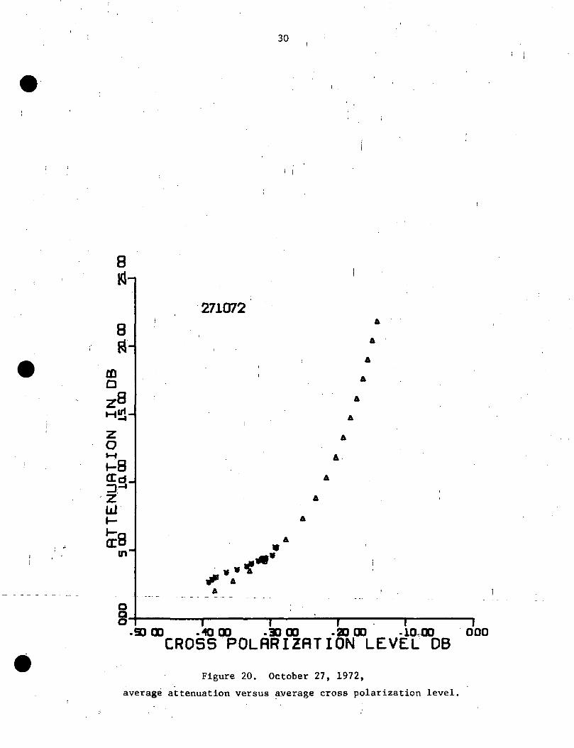
5.1.5 October 27, 1972
Data from this storm appear in Figures 16 through 20.
5.1.6 November 13, 1972
Data from this storm are shown in Figures 21 through 25.

14
UJUJcrorLJ
8-8
8.8
Bo:
Bo:
LJLDa:
u
Ben•8m
8
000 QD 0V QO GB' 00 QE* 00 Qv 00 OS'90 T3A31 NOIlbZiatnOd SSOdD
^rf
8

15
8
Ld
§
40872
8*H
A
gA
A
A
A
* AV
A
AV
\ A
V . *
i i i i iSO CD .40 00 -30..QD -2000 -10 00 000
CROSS POLRRIZRTION LEVEL DB
Figure 5. August A, 1972,
average attenuation versus average cross polarization level.

16
UJLDcrorUcr
cshs.
8.8
8.8
8crX
z:
8CE
*IdIDa:
U
8
o.o
ICJ
U<fl0)
(U
0)
o
CON•H(-4CO
rHoCX
0)Cfiot-lo(U60COM0)
CO
cy.
to
60
dco•H
000 QD 0V 00 QZ- 00 OE- 00 O' 0005'90 13A31 NOIlbZIdblOd SSOHD

17
8* ! .
^i ' •; '•"•" '
4
^ '-**=•i «^r"lr — —
* -a • - 'a jj- — :i • «I
i ' • • ; — ; — »-s — -
, ?^S,..
^; *
•3-:.'=
J ,
"^Pr-~ \ <8 « ^^^-or tC — ' i"^r*" 1Ld IB •- ..«
^
i-
8-9
Bo:-a?
z:r
at!
!8o:
LdLDa:
"UJ-tf?>
uBen
-H
8_iri
-4
a_a
en
<IJ
tH
CO•H
CON
CO
0a,COCOoa
0)60to
0)
CO
A
CM
• iH
VI
r^-' ^H
4-1
CO300
•r^
0)
60•H
QQQ 00 QT 00 OB' 00 OE- 00 OKaa i3A3i NonyzidbiOd
0005'

18
» ^
- *.
crucr
00 CDTE 00^57 OQDT 00 S90 NT NOIlbnN311b
8
^
8.8
Bo:
8or
uID(E
U
Bui•flin
B
000
a§
ccfl
O
f.O
0)
3
CO
Co
CO
0)60CflM0)
'CN
1 —
0)3
CO
0)M
00•Hfn

19
8
UJ13<rtrUor
00 -SZ 00TJZ 00 -5T 00T)7 00 S90 NI NOIlHnN31ib
8.8
Bo:>.-si2:
BCE•g*
UlID(E
u_UJBin
8
000§
to0)3
§
3
(U
0)60
01
CMt~-ON
10300
360•H

20
8
8fl-
CDO
I3'ui
£8in'
180872
..* .1
! I
.3000 -«OD .3000 -2000 -10.00 000CROSS POLRRIZflTION LEVEL DB
Figure 10. August 17, 1972,
average attenuation versus average cross polarization level.

21
Ul
aoru
8,-B
8
80:
r
•"ICEo:
BCE
'ucc
ur,LJBin
8.ui
QOQ 00 01* 00 OS* 00 QE* 00 0^" (90 13A31 NOIlbZIdblOd SSO^D
o8
01cc(0
o
oCO
CO•H0)
CO
CO-H4-1CON•H
Oa.COCOo
a>oocfl
0)
CO
CM
0)
<D
D-O)
0)M
00
OB-

22
croridcr
4
i
4- "' '
4
4
4
4
' -f- —i .•-: V ==.
1 —-%— * ,J ys — *_ 1i ' jr**" — •
: § ^ -=*=^ '
II — _ — - -
•f,'-
1 1 1 1 1 1
8_§
8-S
8x2:T.
-IZ
8(r-a02
uIDCE
UU
•H
8~-i
0_Qr,o
*CO
tHOl
Q)iH
CO
•H4JCON
•H
OO.
COCOO
O
<DocCO
^>
CM
rH'
ONCM
tuf,0)4JCu
C/3
CN
CU
300
•H
000 00 01- 00 CE- 00 CE* 0090 13A31 NOIiBZiatnOd
00 05"

23
8
8
Bo:-ss
See
IDcr
t
i
LJincrorU
U
8
OQ-SZ CD IE 00*51 03*01 DOSao NI NoiienN3iib 000
QQo

24
8
8.15
So:
<rz
B£LJIDcr
UiIDcraUJ>cc
a:u
8
00 oaoa•g

25
8fl-
8
COa
H«
1-8'¥'
in'
oa
290972
-SO 00 -4000 .3000 .2000 -1000 000CROSS POLflRIZflTION LEVEL DB
Figure 15. September 29, 1972, i
average attenuation versus average pross polarization level.

26
UJLD(TCCUJ
or
QOQ GO 01- QO QZaa i3A3i 00 QE 00
8-8
8.8
BorT.
Bcc*UJIDCC
unUJBin
8
o.ao00 05'
0)
cCO
14-1w.-Ia)at
co•H4JCON•H>JCOi-lOa.COcao
a)60co
CO
O4JOO
DOC
- -H

27
, 8
' • i ' ' r§i • . . -
4 ,
• ! ' • '
1 *\ • 1|
<\
. : • : : ' : • « . . .'
4
i • • '! ' I •
i . ,•
; . • ' , . *t ' '
!
, < , ' ' '
«
i
1
«U
» «' '! ^f -ffi s x^41
a: ft rf» :m *7-i J" —
£
i i i i • i
]
8
-S
Set:S *r
?T"i
oUJOL__r^*
"*il!CIIfV*^*
^^>— 1
8cr-ga
ui *icr
ott
-S>oru
_UJBin^«
— jji..j^^^
8-tri
o 'Qo
000 00 OT 00 OE- 00 OE- 00 O-' . _00 Cfi-
tw
rH01
0)rH
C0•H
n)N•HVJtflf^
OD.
W03O
U
0)'
01
mM
CM
O~v
.-1
M
cs
M0)
O
oo
•t^t-l
HIw
360•H
aa "i3A3i NoiibZidbiOd ssodD

28
UJ13oraQJ>cr
000

29
Bo:
uiLDororulor
000
30
s«-
8ft-
COQ
zo
I3'Ld
in'
oQ.
271072
T T I I I90 00 -^0 00 -30 00 -20 00 -10-00 ODD
CROSS POLflRIZflTION LEVEL DB
Figure 20. October 27, 1972,
average attenuation versus average cross polarization level.

31
UJLDcrcrulor
K
8.8
8.8
Bo:•a?
So:
uLDo:
u_UJBin
•Rim
8
aa
000 00 OT 00 QZ" 00 OE' 00 0V* 0005'90 T3A31 NOIlbZIfcbnOd SSOdD

32
U13crorU
(tjor -•
8.R
8
Bo:•a?
z»-i
8CE
u
U_uBin
8
o.Q
000 0001* 00 OZ* 00 QE- 000^' 0005*90 "I3A3T NOIlbZIdblOd SSOd3
<U
0)
co•H4JrtN-HM(flr-lOO.
wMOHO
U60cdM0)
nJ
CMr .c^
>-.0)
i0)
oz
CMCN
a)V43M•Hfe

33
8
LJiacrorUa: _i
T)T
Bo:
bJIDCE
u_uBin
in
uw
000
QJ
cCOo
u«0)
t-lo
enCU
MCO
CO•H4-)cfl
Ccu4-14-1
CO
cuooCOH0)
CO
oM0)N
en0)3iH
CO>
0)C
- CCN cOr- X<T> O
CO
<U
O
rnCN
0)VJ
oo•H

34
uiCToruicr
00"SZ QOTE 00"ST 00"OT 00 SSO NI NOIiWnN31iy
8
I
a:u
Bin•Sin
8
000
a•g
CO0)
CO
CO
CO
CCU
0)00cdl-cCU
CO
cu
CM
cuM
60

35
8
8
CDQ
» V
h-8grdjzUi
in"
RVERRGE
131172A
A
I I I-90 00 -40 00 -30 00 -20 00 -10 00
CROSS ROLRRIZflTION LEVELooo
Figure 25. November 13, 1972, ,
average attenuation versus average cross polarization level.

36
5.1.7 November 14, 1972 !
Figures 26 through 30 present data from this storm.
5.2 1973 Data
5.2.1 Introduction
At the time of writing 7 storms have been observed in 1973 and two
of these brought the highest rain rates recorded thus far in the project.
Table 1 lists the important parameters of the 1973 storms; all are dis-
cussed in the following paragraphs except that of April 41. Data re-i
duction difficulties with that storm necessitate postponing it until
the next report. Because 'of the time delay involved in processing thei
data, storms which occurred after June 1, 1973, will appear in the nextI
report.
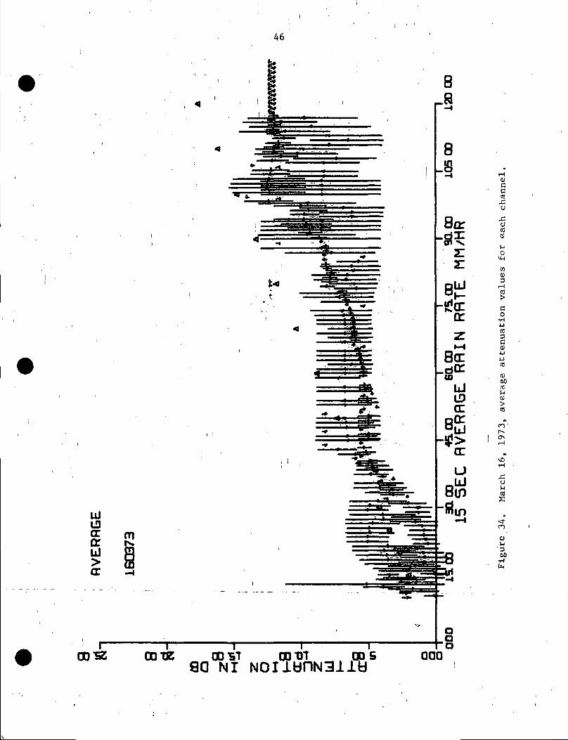
5.2.2 March 16, 1973
Data from this storm appear in Figures 31 through 36. Figure 31
is a scatter plot displaying 15 second running average cross polar-
ization levels taken at successive one second intervals. Data for rain
rates less than 10 mm/hr have been suppressed.
5;2.3 March 17, 1973
Figures 37 through 42 display data for this storm.
5.2.4 April 4, 1973
Plots from this storm were not available at the time of publication
^because of-computer.problems.

8.8
8.8
80:•S5
z:2:
•Kix
Bcr
LJ15o:
R^•«>u
_UJBin
LJ13dorUcr
OJ
8
ooo oooi- oo OB- oooe- ooov. SO 13A31 NOIibZIdtnOd
00 05-

38
8
LJLDorcrLJ
8.IS
z:z:
BCE
LJ
'<r *^ *-"•{•p <y
hi *_UJ 2Bin-81
B
000 0001* 0002" 00 QE- 00 »• ODDS'90 13A3T NOIlbZIdblOd SSOdD

39
8
LJ
o:or
«,
00 00-02 00 -5T 00 TJT : 00 Sgo NX NO-iibnNSiib
8
Bo:x*V
2:
Ct
8cr.go:LJLD
•*>CE
nBui
ooo
aao
OJN
<1)»-lQ)
W
DiHre
01C
s013
CO•H
S
)-i' <aXI
cu
8
D00

40
8
: 4<
i i • i
< . .! ' ' '
i . •
<J
t ' _
<
'• \>
4- - !
' • ' '
^
1 '
«l
! '
, 1'
<\
\
UJ " 1I* • 1UJ q < fd — « <* f
1 1 1 1 1
8
-s
Bet-a?2:
znUJOr
-tacrzt •
BCE'-d^r
UJLDcr
8cr.UJ
— If) ^v^r ^^cru
Bin.
"Wm'""
8-Ui
-»
QDa
••aj3iH
>
C0
4-1
3C0)4-14-1
60CO
CD
re
CM
0\
„
, — |
' 0)X!
0)>o
O-iCNJ
0)•u3to,•H
00 -SZ 00 'OS 03 'ST 03 "QT 00 Saa NT NOiibnN3iiu
aaa

41
srt-
aA-
CDQ
,8
2o
CTo_
ZUi
in
oao1
RVERflGE
141172
r 'i7 r r i9000 -^K) 00 . 3 0 0 0 - 2 0 0 0 -1000 OOO
CROSS POLflRIZflTION LEVEL DB
Figure 30. November 14, 1972, ;
average attenuation versus average cross polarization level.

42
O•H
CDPk
CO•H
C•H
CO
Bo4J
4-1O
CO
•3H
CO,4JC
•HOP-l
CO
COQ
CDC•HCO•PCD
O
M '0)
' "s25 •
^ «c o•rl iH
P§ COr" E3
S §0 O
*"* <5i
^ T ^ 'VI
- I •- H
+ I - H
)_ i|j l Q.
- I + H
+ I + H_ ,. _„bff Jol
V// OH
e# OH:Z# OH
T// OH
5# OH
W/ OH
e# OH
3# OH
It OH '
•aq/ram ' 935^1u'ppjj q^B£ P9SB.X9AV
puooas-gi; ^eaa
•jq/unn (93nBg x XUBaoj scTpij, u99M3ag
_ MW ITTOYT 'MO^ Ta 1* 1 -s[ <j
cT .e o co•H T)
0 4J C4J CO OC/1 M O
3 CDQ W
00rH C
CO -H 0)0 -O BO C -Hn5 W H
00C•H
rH | 'CO to 0)0 « IO 4J -HiJ to H
CD**c8Q
ooo
CMvO
CMCO
CMVO-
•if*-oomoo00CM
vO00
: £mSCMON
oo00
oo
i ^1 CM
VO
CM
r-
vO*CM
-*COCM
«3-
CMCM
VO
ONCMrH
vO
00*ONrH
CO
CN
vrooo
mON
7~«-|-
• vt
vtCO
vOCM
vO
vO1-1
_rjUMCO
•*
m^P
ONCO
ONvO
ONCOCM
morH
r^inCOvO
CMmrHVO
CM
m ;
. ^rHO
vbrH
CM
COrH
mmrH
»3-
r^
r^
mco
^COr^
'<*
ONl-»O,CM
vrONm
CM
vO-O
O
ooCN
coCO
0o
rH
f-jCJ
^
ON
ONrH
r*^CNrH
r>.ON
.00
f^m ;
00CM
CNCO
oCO
vOCM
00CN
rH
*
rH
co
vO
^
vO
vO
rH
p^
CM
ooCO
ON
OvO
CM
mrH00
vO
rHO
vO
ONO
•
vO
ON
o
**rH•rl
<_
vO"
00
rH00
fx.
.CM
00
CN
rHrH
CMiH
•KO
00rH
rH
coCM
0
CO
•K
VO
.
vO
CO
^rH
CM
vOvO
vO
CO
CM
vO
COcorHCM
vO
rHCO
VOCM
iHCN
COCM
^1
ini
ON
ON
00
OvO
^
ON
ON
CMi-H
COrH
0rH
CO
CM
CO
CM
O
co
CO
CO
^>CN
^Vt
CM
mvO
oi-iON
00
00CO
ONCO
inrH
oo
(mcoCM
inrH
vOCM
^
•f
in
VO
oorH
f^
COVO
rHrH
rHCM
CM
COCN
coCN
CM
CO
*m
ON
VO
ooin
rH
r>
ON
vo
CO
oo-a-
CO
. ^. vO
vO
rH
CM
vO
COinCMrH
COCM
O
CMrH
CNCO
CMCM
CM
^3
rHCM
ONCO
rH
0-3-
rHCMCM
mCM
CMON -
S'rH
1
SCNON
'sj.
COCM
r--jv!CM
i»*
. VOCM
CM
r^^^f
COCM
;°00COrH
iVO
rHCN
CM
CM
V?
CM
VOrH
ON
rH
CNO
O
CO
COorHO
OO. CM
'
$
0)CJCCO
0)4-1
0)c•H
00
•H
0)00
CO00
CO•H
CD4JCJCDcoCJCO
cCO
oU
O
-O.OJ
rHCDH

43
8
000 OOOT DOGE GE 00
8.s
80:
<£•—i
8cr'to
LJIDCE
°UJ>o:U
r^8cn
8_tfi
0005-
•Q
oI-lex
too05
co
N•Hi-l(C
oex
tno
vO
03s
3to
•H

44
UJIDo:orUJ
8_a
8.a
Bee
UJ
So:
LJID(T
u^LJBin
8
Q.Q
ooo oo or OD as* OOOE* ODI>' ODOS-90 T3A31 NOIlHZIdBIOd SSOdD

45
LJUJCTorLJ
8.8
8.8
80:
"
• 1
BCE*-8LJIDo:
U«^Bin
8.iri
aa•Q
ooo ODOi' QO oe- OOQE- aoo90 13A31 MOIlBZIdtilOd
00 OB-
0)c(B
O
O«01
tocu3.-Icfl
CO
•H4-Jrt3
4Jrt
oo
ro !
•360
•H
00-52 001Z 00-51 ODD! ,00590 NT NOIlbnN311B
ooo

47
10<u
co
cfl
5(1)
01oocflM0)
X!O
D60
•H
00 TJZ 00 "51aa NI .00 S QQQ

48
1 1 • •
• 1
1 '
'
k
> „ X4 - "l _
* « »^L ; •* ^**%^• a^^
! ^ ' *^*4 »%»*
' Itff^ '
J P
^
U| ^ »d (T) » >*»Q: tv 4
> I'D ^cr -•
•
^< . ' ''*•
i i i i . i - -->
0-aa
CD
8°o-l
•**^|| \
* ^^
^^fc
LJ„-!8_
.Bo' t_|
h-CE
fl "kJM ^^^"^^••4
.Ror'^o
8°-o(T)
- in0a:u
8g)
*rH(U
1 ' Sr-t
- Co
•H4_treN
•H
re•• ^H
ro 0
iH' 0505
, •> O
i H U
XI QJO 60M rere >-iS a)
?>re
vO «
0)4) Mu a)3 J>
•H CP4 0
•H4JreD
(1)4-J
reCJ
- - - - 00-c;Vi
>'J
00*52 ODfZ 00 "5T 00 TH DOS90 NT NOIibPNBlib
000

49
m
8-H
8
8or*re
z:
80:
LJIDor
u_uBin•film
8.id
a.Q
n i i i i000 00 01* 00 OS" 00 OE" 00 0^* 00 05
90 H3A31 NOIlBZIdblOd SSOfcD
o1-1CL
Oto
g03N•H
Oa,toCOo
ro
Oi-irt
oo

50
LU13ororU
,m
tv
8.8
8.8
80:•a?
z:2:
•idtro:zt-4
Bo:*(0
UJLD<r
cru
^UBin
8
aa
000 00 01- 0002- 00 OE- OOO' 0005'90 "13A31 NOIlbZI8b"10d SSOHD
gctf
onj01
<D
0)
co•H4-)CON•H
COtno
a)ooco
o
oo
oo•H

51
8
uUcrorU
m
OOOf 00 OV GO OB' ODOE- 00SO 13A31 NOIlbZIdblOd
8_8
Ber
a:
BCE
UIDo:
j1*fSi
U_uBin
"Win
8
OO 05'
oa'O
co•H4JrtN
oa.to<DO)-lo
0)60to
UMCO
4)M3OC•H

52
4
1ortm
wQ)
'o: co
*
cCD4J4Jrt0)
CO
p>cd
f.oMn)
oruor
rn60
03-SZ 00IK COST Op-QT 00 S90 NT NOIIBnN311B
000

53
LJiflor5or
m
cote 00-57 00 t)T 00 !aa NT NoiibnN3iiy
8
8
Bo:
Bara:uIDcc
uBin
8
aaa
a8
CO
,Q>i-l
CO
CO•H
3
(U
0)oo
a)>tc
a)M
oo

54
8
8a-
CDQ
oi*-«l\-B
UI
in'
oa
RVERRGE
170373
9 A,
OTT r.9000 --4O 00 .3000 -2000 -10-00 OOO
CROSS POLRRIZRTION LEVEL DB
Figure 42. March 17, 1973,
'average attenuation versus(average cross polarization level.

55
5.2.5 May 23, 1973
Data for this storm appear in Figures 43 through 48. •.' I
5.2.6 May 26, 19731 : . •
Figures 49 through 54 present data from this storm.
; 5.2.7 May 27, 1973
Figures 55 through 58 display data for this storm. Apparently a' i !
transient somewhere in the system kept the PB 440 computer from re-. • i
: I :
, cording sufficient data to generate values for + to - cross polarization
and + channel attenuation.
5.2.8 May 28, 1973
Figures 59 through 64 display data from this storm.

56,
8
8_8
80:•^
*£
8<r
LJIDo:
Iu
Bin•film
8U«i
000 0001- 00 OK' 00 OE- 00 O' ODDS'aa 13A31 NOiibziabiOd
aao
4-1O
M01
Ow
o•H4JOJN
•HM«
O. p.
COOJo
co
sPO-3-
60

I
57
LJ13cror
000 0001- 00 OB' 00 OE- 00 O90 13A31 NOIlBZiablOd
8_8
8_S
8tr
-^
Sen
uIDo:
a£-*£
u_UJBin
8
0005'
aaa
oCC
o
o
OJ
0)
0•Hu«N•H
Oa,a;wo
atocd\-t<u
COCM
a)J-l3MTl

58
UUororLd
or
8.a
8_s
Bor
o:
Bcc
idisor
i or
u,_,UJBin
•tiin
8
0)
0)
co
caN
OEX
10U]o
00to
CO
CTi
COCS1
tdS
36C
fan
000 00 OT 00 OS' 00 QE* 00 O90 13A31 NOIlBZIdbnOd
0005'
oao

59
8
UJID(TorUJ
cr
mx
8us
OD-52; ooie oo vr OQ in oosaa NI NOiibnN3iib
8(T
• •
8cc
UJIDCE
u_UJSin
8
000
a.aa
0)
ccfl
oCOfl)J-lo
CO01
r-l
co
CO
aG)4-1
4-1CO
OooCO
COc-i
vOo-
60•rl

60
UJL3
>or
00 "02 00 "ST 00 tW 00 S90 Ml NOIlbhN311b
8.8
8.8
Bo:
•£CE,0:
Bo:
U19CC
8^
•*lU
8$
8.ul
000
o0
•Q
3H«
CO
•H4Jtaa(LI
111t>0rt0)
roCM
sl-
tU
360•H

61
8Kh
1 !
as-
co• 1 • Q
5s-! Z
Ot**4
H8
Uii—£8
in"
oa
RVERRGE ,
i
230573A
1,
i •A
1 |
A
. A , . ' "
• A -
A • i ' '
/A£ ' V » - •
^Ajf^
1A _ ' I i
.9000 .4300 -3000 .2000 -1000 000CROSS POLRRIZflTION LEVEL DB
Figure 48. May 23, 1973,
average attenuation versus average cross polarization level.

62
000g
Of 0002-13A31 NOIib
OE* 00 OKdBIOd
8.8
8.3
8cr
z:z:
f «
Bar
uIDcr
CE
U
Bin•Sim
8
0005-
aao
o^1a
COOtoco
•H
M•H
ct)
.0
en(AooA
fl
ICTl^*
(U
o•H

63
UJ
UJ>
000 GO QT 00 OB* 00 OE- 00 O90 H3A31 NOIlbZI^blOd
8-a8
Bo:-85
*£
8(E
UJLDCE
U_UJBin
•Stin
8.ri
oo 05-
o•i
(Uc
£.UCO0)
0
cu
g•H4JcflN
Oc.COCOo
III00CflMOJ
CO
fO
vOCN
Om<uM3oc•H

64
UJLIDcrcrU
I
V .^
8
a.aooo oo or 0002- OOOE* ooo*-- coos*
SO 13A3"l NOIlbZI&fcnOd SSOfcD
8.8
Bar
rr
» — *Bo:
LJIDor
U^UJBin
8
0)
0)
co•H
N•H
Oo.totoo
QJOC
0)
efl
\OCM
oc

65
8-B
8
I1 < ' . '
. ' • I
I\
' '••,• . ' . « ', '
.
' ' < '
1
1 < •1'
11
'« i ' '
<I•
. ; 13' • ' * J J.
* 3
13* 3U . I ^13 Sicr m li?voc tx. -*z*LLJ jfl T
:=^5-
cr cl ** .'
-•
80:"en?
21 'z:
oUJBi
-ido:LJu
2_»— i8CE
~s
LJID<r
a orOQJ
— tp^
a:ui, i
Bin~Wm
-H
8-at
°
aa
i i i i & i o00-52 00 TK 00 -51 00 HI 00 6 000
90 NT NOIitinN31iti i
§.co
0
0)
oM-i
(0
rHJO
Co-H
CO3C0)4J
tB
a)bOtoa)to^
fl
ON
^\oCN
cd2
•csm0)
3oc
•H

66
CO0)
g•H
(0
c111JJ
<u00
0)
n)
co"
Oi
voCM
COIT)'
0)M
00
OD-5Z 00 -02 00 'Bt ODTJl 0090 NT NOIlbnN311b -
000

67
oQ
•: ! . !
, i 'i •
^ .
* '* « -rft 1*9 i
< ' : •' ' . * i
1 ' '' <• •; ' i
1.
«h
» 43 BB» ^9L^ ** "J
UJ ' " ' i t13 » <»^^* i ' .» ^UU Ij . ; ^L
III U1 . w •
> S 4a: N
i
,1 , ii • i • i i i
a
i £>
8°o— '
"•*?UJ, >
UJ
8" T1
_jj.
^% t13 r^ ^^*»fHH
h-a:
_^ |M 1Ll IT poi— i|L| rt
" 'CC_JO
^% nD
nil")— ^in• U J
Ooru
8 '
Si00*SZ 00 TZ 00*51 00*01 005 000
at>Q)
GO
•H
CON•H
cflr-lO
• P.
r^ toON tfli-l. 0
•> uvOCN (U
00>i tOCO >-iS <u
>cO
m 3(0
0) ^>-l OJ3 >tt>•H C[LI O
•H4JCfl3
0)
4-1
CD~ 60
CO
•U
CO
SO NI NOIlbnN311ti

68
8.8
8.8
Bar•a?2:r
pUJ~
8CE
LJLDCC
u
8
o.QO
ooo QO m- oo oe- ooios- oo13A31 NOIibZIdblOd
oo 05-

69
UJ13oror
cvj
8-8
8.8
8CE
-gLJIDcr
u_UJBui
8
Oo
QQQ 0001- DDK- 00 OE' 00 O' QQ 05*90 "13A31 NOIlbZiatnOd SSOdD

70
IDC£o:
00*52 00 TK 00 "ST 00 DT 005aa NI NOiibnN3iibi
oao

71
8
8fl-
COQ
'Zo
Zill
in'
a§•
RVERflGE
270B73
' -' .«'
•90 00 -4000 -3000 -2000 .1000 000CROSS POLflRIZRTION LEVEL DB
Figure 58. May 27, 1973,
average - channel attenuation versus average - to + cross polarization levels,

72
8-8
8
LU
80:
LJID<r
u^LJBin'Win
-H
8
000 00 01* 00 OS' 00 OE- 00 QV90 H3A31 NOIlbHiablOd
00 CB-
aao

I 73
uIDa:a:ui
8R
8
Bo:
•Kla:a:
Bo:
UJina:
•*£u
_UJBin
8.iri
000 00 0V 00 OS' 00 OE- 00 Oaa "i3A3~i Noiibziabnod00 OS"
a.aa
r-l4>cto
to0)
(LIrH
O•H4JtON
toO
COCOOHU
0)00to
£CO
00(N
a)M
3,

74
UJ
UJ
m
000 OD or _ OD,PB- QD.QE; __ go
8.8
8.S
8xX
tr
Bo:
uLDoc
a:u
8tn
8
90 13A31 NOIlbZIdblOdft QOtB-
oaa
CO
0)
a)
o•H
N•H
COrHoa.COwo
a)Mcfl
0)
CO
ooCN
X
S
vO
P60-H

75
8
V 1 . .r | ' .
• ' • < ' • ' .
4
1 ,
| 1
«' - ,
' ' : ' ' ^
< ,
I
' '
<
' 1
1
1
1 ' '
, ' « , ' '
1 ' '
4 ' .
.
' ^
«Ul13 -1s K • , ! .
§ | :4-,:
' '"••"
i i i i iCD -52 (DTE _ CD-5T ^ .CD.T1T _ . .GO S 00
8
-9
80:_ ^^^
"~8 x5-^^
roliJ
SK
"^ct
»-H
BCE"S°"
uIDcr
-S<ru
_UJBin^_ .— H _
-H
8-irl
-4
OQ
0
•H
CcCO
"o
^^O
(U
OU-l
to(U3
CO
•H|J
cfl3
(U
4JCO
0)00CO
ar
CO
+,•
ro
rH
OtT
cflS
•CMvO
(Ut-l36C-
i 'H(
gaNi

76
8
UJ
>cr
OOSZ 00 IE 00 57 CD 1)7 00590 NT NDIlBnN311b
8
Bcc
'K
Bcr•g*
UJIDo:
2*•*£u
_UJ8(n•fifin
8
ooo
0QO
CO(U
fHCO
CO•HJJ(8-3
0)
OJto
0)
rnr>ON
'00
n)S
vO
0
00•H

77
1
' • ' ' • oQ
j
i . 1 ' '|
^ v « « v<4
4<
'«
.'. -UJ « <ID < » »o: m » *or r* <U IS *^> i H • ^o: N
i1 ; i
:
i i i i i
-o
CD
8°CD ^^
^ *^I|I^'
LJ
8".a§
^*^i _r—
o:ohvl
" -CE_lO
8°-nlfi
,inoo:U
8
(U
(U| T-H
co•H
tfl
•H
rat-Hoo.wCOo
CO O
^ CD^H 00
- Vioo a)CM >
n co. S 3
CO(-1
• . QJ
**^" J^
a gM -H3 JJ00 fl•H 3
^ §j-l4-J03
! a)00
0>
re
•DOSS ODT2 C O S T D O T H 00 Saa NX NoiibnN3iib -000

78
5.3 Summary
Figure 65 is a cumulative scatter plot of all the 1973 depolar-' ' ' !
ization data presented in this report.I
Figures 66 and 67 illustrate the average cross polarization levels
by channel for all of the 1972 and presently available 1973 data
respectively. Figures 68 and 69 present similar data for both channels
together. .l . • ' -
Figures 70 and 71 display the 1972 and 1973 average attenuation
values for each channel 'and Figures 72 and 73 illustrate the average
values resulting when data from both channels are combined.
Figures 74 and 75 are plots of average attenuation versus average• i
cross polarization level for 1972 and 1973 respectively.

79
LJ>
<T_J13r.
8.8
8.8
Bo:•«
z:z:
CE gor «s
Ben
LJIDo:
)0r
cru
Binhsiin
8
oa000 0001- 0002- 00 OE- OOOV- 0005-
90 13A31 NOIlbZIdblOd SSOdD

80
«•
*
UJLDoror
8.8
8S
80: -5
So:
8
LJl£>CE
5
U_llJBen»in
8
a.a
000 00 OT 00 OB' 00 OE- 00 Ok-' 00 05'90 H3A31 NOilbZIdblOd SSOdD

UJ(JcrorU
8.8
8
Bor•a?
z:
-si'LJLDo:
Uhi
Bin"Sin
-H
8
oQ_ ________ _ ___ ___
Qoo oo or oo oz- oooe- ooo*-- oo os-aa H3A31 NOiiuzidbnod ssoiiD

82
8
UJ13oro:U
000 00 0V 0002V QQOE- 0090 13A31 NOIibZIdbnOd
8.8
8cr.(D
uLDo:
pCC
M %nBin
Kflin
8
0005'
a.aa

M I13(Torulcr
-1...
8.8
8.is
8or
z:
8cc•a*
LJIDCC
ustfi
•Sin
8
000 0001- 00 OZaa i3A3iDOGE 00 O 0005-
oQO

84
1 ~
c
£1u
o«0)
co•H•U
Cai
0)oot\)
CNr^cr\
00
QQQ

85
,-H0)C
03.Co
o<oCU
COcu
Co
to
cu4-14JCO
cu00COMa)cfl
o4Jen
•HCO
r-
QJ
60
90 N I - N O I I U H Noao

86
COa)
co•H4JTO3C(U4-1
OJoccfl(-10)
00•H
00*52 00 te OQ-5T 001)? ODSaa NI NOii8nN3iiy aao

87
COcu3
Co
c0)
0) •00COM
O4JCO
X•HCO
CTii-H
CO
I —
300
DO'S90 NI NOIibnN31ib
GOO

88
8«•
8
£0O
CEd.H-»Z
in'
aa
flVERRGE
*\-:O ^ ~ J I T I I I
•5000 --10QO -3000 -2000' -1000 000CROSS POLRRIZRTIQN LEVEL DB
Figure 74. 1972 average attenuation
versus average cross polarization level,

89
8
8
CDQ
zPus-I
'Zo>H
h-S
Ul
in'
o8;
RVERflGE
A i
• iSO 00 -^O 00 -30 00 -20 00 -10 OP 000
CROSS POLflRIZRTiON LEVEL DB
Figure 75. 1973 (six storms)iaverage attenuation versus average cross polarization level,

90
6. Literature Cited
1. C. W. Bostian and W. L. Stutzman, "The Influence of Polarization onMillimeter Wave Propagation Through Rain," Semi-Annual Status Report II,NASA Grant NGR-47-004-091, VPI&SU, Blacksburg, January 1973.
i .2. C. W. Bostian and W. L. Stutzman, "The Influence of Polarization on
I Millimeter Wave Propagation Through Rain," Semi-Annual Status Report I,! NASA Grant NGR-47-004-091, VPI&SU, Blacksburg, July 1972.
3. J. A.(Morrison, M. J. Cross, and T. S. Chu, "Rain-Induced DifferentialAttenuation and Differential Phase Shift at Microwave Frequencies,"BSTJ, Vol. 52, pp. 599-604, April 1973*. i
4. T. Oguchi, "Attenuation of Electromagnetic Waves Due to Rain with |! Distorted Drops," J. Radio Res. Lab. Japan, Vol. 11, pp. 19-44,
January 1964.
5. T. Oguchi, "Attenuation and Phase Rotation of Radio Waves Due to Rain:'• Calculations at 19.3 and 34.8 GHz." Radio Science, Vol. 8, pp. 31-38, !
January 1973.i '.
6. A. F. Stevenson, "Solution of Electromagnetic Scattering Problems asPower Series in the Ratio (Dimension' of Scatterer)/Wavelength," JAP,Vol. 24, pp. 1134-1142, September 1953.;
7. D. T. Thomas, "Cross Polarization Distortion in Microwave Radio Trans-mission Due to Rain." Radio Science. Vol.! 6, pp. 833-840, Odtober 1971.
8. -H..C. van de Hulst, Light Scattering by Small Particles, New York:John Wiley and Sons, Inc., 1957, pp. 28-34.
i9. P. A. Watson and M. Arbabi,' "Rainfall. Cross Polarization at Microwave
Frequencies." Proc. IEE (London). Vol. 120, April 1973.
10. P. H. Wiley, C. W. Bostian, and W. L. Stutzman, "The Influence ofPolarization on Millimeter Wave Propagation Through Rain," InterimReport I, NASA Grant NGR-47-004-091, VPI&SU, Blacksburg, June 1973.

91
7. Appendix; Considerations in RF System Design
for Cross Polarization Measurements
7.1 Introduction ;
:The RF system design, construction, and testing for this project
were done by R. E. Marshall. Mr. Marshall wrote an M.S. thesis about
the RF system and included in it both new information developed by this
project and information from widely scattered sources in the literature.
As Mr. Marshall's thesis will be of considerable interest to other
designers of depolarization experiments, most of it is reproduced in
the pages which follow,! It involves the design of a transmitter and: . ' i
receiver to meet the following criteria:
Transmitter '
11. Operating independent channels: 2(+45° and -45° polarization)
2. Switching capability: transmit or no transmit remotely selected
forieach channel!
3. Polarization isolation: > 40.0 dB
i
Receiver
1. Operating independent channels:. 2(+45° and -45° polarization)
2. Polarization isolation: > 40.0 dBt
3. Dynamic range: > 41.0 dB
4. Easily interpreted transfer function

! 92 . .
i SECTION 7.2 ' ,,
: RECEIVER
i '
7.2.1 Scope of Section. . . ; - - j
Presented in this section are typical receivers for attenuation
i • • ;and depolarization measurements, design calculations for the VPI&SU
17.65 GHz transmitter, and suggested improvements. \
! .7'.2.2 Typical Receivers
Once the path is defined, the receiver design is primary. Optimum
'receiver performance is obtained easily if one is not working under
the restriction of a specific received signal level. This restriction
fixes the upper bound of the dynamic range and forces the designer to
find hardware that will fit the situation. It is simpler to design theI ;
receiver and then provide the proper transmitted power.
Figure 2.1 is a block diagram of a receiver that will measurei
attenuation. Single conversion is used because it is economical,
introduces less noise, and is easily accomplished with available milli-
meter wave components. The RF amplifier and mixer are usually found
commercially in a single "black box." Noise associated with wide band-
widths and high noise figures is a major cause of shortened receiver
dynamic range. Bandwidths as low as 10 MHz are available with most
commercial millimeter wave mixer-preamplifiers; Typical noise figures
are from 9.0 to 10.0 dB. The local oscillator must be stable because
of the narrow bandwidth requirement. A 50% savings is'usually realized
when mechanical tuning is chosen over voltage tuning; voltage tuned

93
Detector Mixer
L. 0.
Figure 2.1. Attenuation Receiver

94
; oscillators also require more expensive and stable power supplies.| !
Detector choice is based mainly on the transmission mode used, but a
linear transfer function will result in easier data analysis.
Figure 2.2 is a block diagram of a dual channel receiver used for
cross-polarization measurements. The mixers, preamplifiers, local
oscillator, and detectors are identical to the components used in the
attenuation receiver. The local oscillator is shared by both channels,! ' . : . • • '
which greatly reduces cost and tuning difficulties. The relative cost, j
of the local oscillator allows the addition of another channel fori
about 70% of the cost of a single channel receiver.
Figure 2.3 is a block diagram of the VPI&SU 17.65 GHz, CW,
receiver. The isolators insure polarization isolation, and the
attenuators control local oscillator power to the mixers. The use of
uncalibrated attenuators here will save about $300.00 per attenuator.
7.2.3 Choosing Receiver Componentsi i
The elimination of cost and noise due to a transmission line
between a pre-amplifier and a mixer warranted the use of commercially
•available mixer-preamplifiers for the VPI&SU receiver. A balancedi
mixer with an orthomode coupling mechanism was chosen because of its
high isolation between the local oscillator port and the RF port.
Local oscillator noise suppression also prompted the use of a balanced
mixer , because local oscillator noise reduces the dynamic range of
the receiver..••—.
The mixer-preamplifier chosen waa an RHG MP015/2CI The specifi-
cations are listed below*

95
Detector
Detector
Mixer
PowerSplitter
Mixer
Figure 2.2. Depolarization Receiver

96
LOG
AMP
LOCAL
OSCILLATOR
LOG,
AMP
MIXER
MIXER
/r
Figure 2.3. VPI & SU Receiver

97
Gain: 25 dB ~ ,i
LO Injection: 0 to +3 dBm
! . LO to RF Isolation: 20 dB
Input VSWR: 3/1
IF: 30 MH*i • ,
IF Bandwidth: 10 MHz1 ;
: Noise Figure: 9.8 dB. : . ' ' : '
An ideal figure can now be placed on the receiver sensitivity.
This sensitivity will be a best case value and will be adjusted by• . I
local oscillator noise.i i
S - -174 dBm -f 10 log(BWXF) 7
S = CW sensitivity in dBm
BW e IF bandwidth in Mtiz"! | - • •*• i
F « noise figure expressed as a ratio
Diode conversion loss is included in the noise figure.i
S = -94.2 dBm',, • ' I ' • •
The orthomode coupling system does introduce the problem of ai
3 to 1 VSWR. The mixer must receive a 0 to +3 dBm local oscillator
signal above the reflected local oscillator power. Below is a cal-
culation of minimum LO power required for proper operation.
|p| a magnitude of the reflection coefficient
|p|_= (VSWR - I)/(VSWR + 1) •: 1/2i _ ' _ _
t+r -~1.0.s
t = transmitted power coefficientt
r = reflected power coefficient

98
1/4
3/4
PL_ = local oscillator power
P t = l m wLO
LO '
L
"** (minimum value)
8/3 raw (maximum value)
p (total) = 16/3 mw (maximum value)IA) ' ' . .
Since commercial specifications tend to reflect the best possible
values of VSWR, it is best to buy more LO power than is needed and then
put an attenuator in series with the mixer LO input. This also allows
the receiver to operate longer if the LO power decreases with age.
Receiver stability is almost completely dependent upon locali ' • i
oscillator stability with a fixed frequency CW receiver. The bandwidth
of the receiver is 10 MHz and if the LO drifts 5.0 MHz or more, an
attenuation measurement error of at least 3 dB would occur. Cross-
polarization data would! not be erroneous because each channel would
fade equally. The danger to cross-polarization measurements results
from a loss in dynamic range. As the LO drifts, the IF will drift out
of the bandwidth and the detector output will drop. This forces the
upper end of the dynamic range to move towards the lower end and! •
Jeopardizes the lower rainfall rate data. Below is a calculation of
required LO stability.
Frequency • 17/62 GHz
Stability- ±(BW/2) (100/P) - t y~|j - ± 6.0284%
This value of stability must be good over the temperature range

99
che LO will experience. If.temperatures are extreme, an environmental
chamber may be more economical than buying an LO that is stable over .1 t • ' , '
Che extreme temperature range.
Noise generated by the LO causes a reduction in the dynamic range
of the receiver, by causing a. detector output when no RF is applied to
che mixer. Noise problems can be minimized by choosing the most stable. . i
LO available and picking an IF bandwidth as small as possible for that
stability. This also aids in tuning because the detector output will
have a sharper maximum for the smaller bandwidths. The value for
allowable LO noise will vary depending on the type of detector used,• ' • . ; . i ' '' . ' i \
and for that reason, a more detailed discussion of LO noise will be1 ' i
presented after the section on detectors. Below is a list of LO
specifications defined to this point.
Frequency: 17.62 GHz . '
Stability: ± 0.0284% , '
Power: 4/3 to 8/3 mw (per channel)
Tuning: Mechanicalt iDetectors
As stated before, the dynamic range of the receiver must be greater
Chan 42 dB, and the transfer function should be as elementary as possible.
For these two reasons, the logarithmic amplifier is an ideal detector
for attenuation and cross-polarization measurements. Figure 2.4i
represents the input vs output characteristic of an RHG LST 3010 MAT
log amplifier chosen for the VPI&SU receiver. The linear D.C. output
vs input dBm is "tailor made" for attenuation or cross-polarization

100
. • o.
o1-1
oCMI
Oen
^—^
S
Oir>
OvO
oCO
oOlI
0)•rl
I
OP -Hsj- v-' HI «
H 005 O
cs
Q)M3 •00
CM
XfidlQO

101
measurements. Below is a list of the RHG log amplifier specifications.
Frequency: i 30 MHz ; .i i
Bandwidth: 10 MHz
• • •Input Impedance: 50 ft ;
Input VSWR: < 1.5-1
Dynamic range: > 80 dB
' • Log accuracy: i 1 dB over 80 dB range 1
It is now possible with the aid of Figure 2.4 to calculate the
maximum allowable LO noise. A dynamic range of 50 dB was used instead
of 42 to insure that all the data is observed. A 50 dB dynamic range
corresponds to a -50.0 dBm LO noise signal.
DETECTOR INPUT VSWR » 1.5 to 1 • '
t + r =• 1.0
t "- 24/25
25 —5p_ » noise power incident to the detector - -57- (10 ) mw
PND " ~49'8 dBm
IF gain - 25 dB
Pmn " -*9.& dBm - 25 dB - -74.9 dBm 5 local oscillatorMJLiU j • !
i> noise power.
j Since this is a two-channel receiver, the total allowable LO noise is
- 71.9 dBm. i ;:
8 "~ •Shurmer suggests the use of Gunn oscillators for local oscillators
' ! •when the IF is around 30 MHz because of their low noise properties.

•' ~
102
The Gunn oscillator is very economical as well because it can be
mechanically tuned and requires only a low DC voltage for power.
The local oscillator chosen for the V?I&SU receiver is an RHG
G01K131 mechanically tuned Gunn oscillator with the following specifi-
cations .
Frequency: 17.62 GHz
Stability: 15 to 35° C' . • . j- ' • '•
Noise: - 110 dB
Power: 25 mw
The output of the detector is 0.5 VDC when full LO power is allowed to
the mixer and no RF power is present at the mixer. This sets a lower
limit on the dynamic range of 68 dB. When the attenuators were set
for 4/3 of a milliwatt LO power to each channel, the detector output1
was 0.4 VDC corresponding to a 71.4 dB dynamic range.
The RHG mixers used have an LO to RF isolation of 20 dB. This
value is far short of the 42.0 dB polarization isolation needed as
predicted in Section 1. A 24 dB isolator was placed in each channeli
to insure the minimum polarization isolation.
PI - I + TX + M + A
PI » polarization isolation
I » isolator isolation « 24 dB
T => E plane tee isolation D 3.0 dBJ
MJ» mixer isolation. «?_20.0 dB
A_ o attenuator isolation - (0 to 25 dB) ::';-,
PI •> 47 dB (minimum value)
• 72 dB (maximum value)

103
The 24 dB isolator at the LO output is strictly for VSWR pro-
tection for the L.O., because a lossless reciprocal 3-port can never.
9be completely non-reflecting. ! ;
The two attenuators are used for adjusting local oscillator power
to the mixer. The local oscillator power is 25 raw and each channel
requires at least 4/3 mw for proper mixer operation. The amount of
attenuation required is given by A.-.
A Q = 10 log (y . •£> « 10 log (g=)
A Q = 9.75 dB.
Commercial uncalibrated attenuators for K band are available inu
0 to 25 dB varieties or higher, so a 0 to 25 dB uncalibrated attenuator
was chosen for each channel. Since LO power to the mixer is the
important parameter, the attenuator setting is made by monitoring
power from the attenuator. The use of uncalibrated attenuators saved
the project $600.00.
The E-plane tee splits the local oscillator power. It is the most
economical device available for that purpose, but it does cause the
phase of each output leg to be ,180° apart. Figure 3.6 represents an
E-plane tee and its scattering matrix. Ports 1 & 2 are the mixer legs
while port 3 is the local oscillator leg.
•i 1/2 1 -/2
a
— _ —,—. i
If ports 1 and 2 are matched then a. and a« are both zero.

104
2 - 2~
From these calculations it can be seen that the voltage at port 1 is
180° out of phase with the voltage at port 2. After filtering, the
mixer outputs are: ;
. " . i i
! a2eLOeRFC08([u)SIG " \0]t) (p°rt 1} i
a2eLOeSIGC08([uSIG '
ij> = TT for E-plane tee ;
Since the detectors respond to input dBm, the phase of the mixer output
is of no concern.
7.2.4 Suggested Improvementsj
The addition of a calibrated phase shifter in one channel would
allow the experimenter to set the clear weather phase difference between
channels to 0°. This would greatly simplify received signal phase
!measurements.
7.2.5 Final Receiver Specifications
Figure 2.5 is the transfer function for the VPI&SU 17.65 GHz
,receiver. Both channels are identically calibrated. Below is a list
of the final receiver specifications.
Dynamic Range: 71.4 dB
Channel Isolations > 60 dB
-St.

105
ao
u§
M0)
«W(0caVJH
a)o
c/]
CM
0)Hs00

106i
SECTION 7.3
, TRANSMITTERi
7.3.1 Scope of Section
Presented In this section are typical transmitters for atten-
uation and depolarization measurements, design calculations for the
VPI&SU 17.65 GHz transmitter, and suggested improvements.
7.3.2 Typical Transmitters1 % '
Figure 3.1 is a block diagram of a typical transmitter for atten-
uation measurements. The source should be stable in both frequency and• /
power. If the source is capable of delivering more than the requiredi '
power, an uncalibrated attenuator can be used to reduce the transmitter
output to the design level and to hold it there as the source ages. An
isolator should be used to protect the source from a high VSWR encoun-
tered during switching unless one is provided Internally with the
source., A directional coupler and a power meter will allow continuous
. monitoring of the output power. It is often convenient during antenna :i
alignment or receiver checks to shut down the transmitter power. Ai
waveguide switch and a matched load will allow the transmitter power to
be dissipated safely when so desired.
.Figure 3.2 is a block diagram of a typical transmitter for cross-;; - i
polarization measurements. The components are identical except for the
power splitting device. The VPI&SU 17.65 GHz transmitter is identical.: • . I . .*£-,to this except that a 3 dB coupler is used as the power splitting device
and an uncalibrated attenuator is placed In one channel to Insure equal

107
I
L
1s
. Kwitch
1L_ fc1 1 "Hr*1 1 Source
Figure 3.1. Attenuation Transmitter
.. i

108
SWITCH
POWER
SPLITTER
SWITCH
K
SOURCE
Figure 3.2. Depolarization Transmitter

109
V
Switch
Switch
Source
Figure 3.3. VPI&SU Transmitter

110
outputs.
7.3.3 Necessary Transmitter Potter and Stability
The power required depends upon! receiver saturation level, path ;
loss, antenna gain, and transmission line loss. Below Is a calcu-
lation of the required transmitter power for the VPI&SU 17.65 GHz
transmitter.
L = path loss - 21.98 + 20 log (r/X) 10
r = path length
X = wavelength
X - C/F = 0.017 m
L - 120.48 dB
PT = power transmitted - PR + L - G.-
PD = necessary receiver input power • -J.6.78 dBm ;&
G = total antenna gain - 90 dBAX
P_-•» 13.7 dBm or 23.44 tnw
For a two channel transmitter, the total output power must be 46.88 mw.
The stability of the source at the required power level is Just as
important as local oscillator stability. Below is a calculation of
required source stability for the VPI&SU 17.65 GHz source.
S = stability - ± (BW/2) (100/P)
BW 5 bandwidth - - - - - -
E = frequency :
S - ± (.01/2) (100/17.65) • ± 0.028Z

Ill
7.3.4 Component Selection ;
The source chosen is an RDL POOR(3) crystal oscillator and
varactor chain multiplier. The specifications are listed below.
Frequency: 17.65 GHz
Stability: ± 0.005%
Power Output: 70 mw minimum
Temperature: 0 to 50° C '
Spurious Noise: < - 40.0 dB
Mechanical waveguide switches were chosen because of their high
isolation between ports. The isolation must be as great or greater
than the polarization isolation of the receiver or erroneous cross-
polarization levels will be observed. The waveguide switches chosen
were Waveline 777-E solenoid operated, double pole-double throw, current
holding switches.
7.3.5 Transmission Line Components
A major concern in the design of the transmitter was the VSWR
Introduced by the waveguide switches during switching.
Figure 3.4 is a top view of a Waveline 777-E switch in the rest
position. For this explanation port 1 is the source power input, port
4 is matched, and port, 2 is the antenna feed. The 90° circular are
from part 1 to part 2 is 1.42 inches long. The dimension of the wave-
guide short wall is 0.311 inches. When the switch is activated,'part 1
Is fed to part 2 and part 4 is fed to part 3. As the cylinder moves,
part 1 is shorted for 1.11 inches of the 1.42 Inches of movement. If

112
oXoO
coV
•34J
O6400
(U•o
. oI
•»•
CO
0)
o O Oo jcs jao\ o> w

113
the cylinder moves at a uniform velocity for the 100 msec switching
time, the short will last 78 msec. The short is not perfect however,
and a VSWR reading in 78 msec is difficult to obtain. In order to get
an estimated value of the VSWR, a shorting plate was placed across partl
4 and a slotted line was placed in series with part 1. With the source
transmitting and the switch deactivated, the VSWR was 25.0. Under
operating conditions, the short will not be this good because of the
small clearance between the rotating cylinder and the four ports
1*1r i
P,,
„ VSWR-1 . 24 _ Q .VSWR+1 26 °' '
0: reflected power coefficient *> \g\ - 0.852
= power reflected «• r (source power) » 25 r « 21.3mw
Not only must the source be protected from this reflected power,
but the reflected power should not be coupled into the other channel.
Below is an analysis of a 3 dB coupler used as the power splitter.
Figure 3.5 represents a 3 dB coupler and its scattering matrix.2c = coupling ratio - 1/2 (for a 3 dB coupler)
a1 = /50
a. » 0 (part 2 terminated with a matched load)
a. a /21.3 mw (voltage reflected when switch activates)
bl-V.v
» , «
o i/1/r i//rI/ .2. .1.0. 0_
i/vT o o> . »
i
« :;0
/5O
/r

1 1-
114
I
0 I//2" I//2"
I//2" 0 0
0 0
Figure 3.5. 3dB Coupler and Scattering Matrirc

115
PDO = power reflected to source « 10.65 mwHo
When both switches are activated simultaneously, the reflected power
will be 21.2 mw.
50 r - 21.3
r = 0.426 - |p|2
|p | - 0.653 .
•+|P I.VSWR 4.76
Discussions with RDL technicians convinced project personnel that the
RDL POOK(3) source would withstand a 4.76 VSWR for 78 msec.
The 3 dB coupler also provides excellent channel isolation for
power reflected during switching.
0 1/»T 1//T
1/../5T. o o
0 0
lb = - (contains no reflections from part 3)2 -
& •b_ • 1 (contains no reflections from part 2)
The 40.0 dB coupler allows the source power to be continuously
monitored. The coupling ratio was carefully checked for accuracy at
17.65 GHz and was found to be 40.0 dB.
The attenuators used are un calibrated with a range of 0 to 25 dB.
The high values of attenuation were
attenuators were not available. The VSWR of each attenuator was 1.15
maximum.
never used, but lower value variable

116
7.3.6 Transmitter Performance
The VPI&SU 17.65 GHz transmitter was licensed in the spring of
1972 as a contract developmental station in the experimental radio
service. It was assigned the call letters KQ2XOC. In accordance with
FCC regulations, the transmitter source was provided with a remote
"on-off" circuit located adjacent to the PB-440.
Below are the transmitter specifications measured during the final
testing stage.
Frequency: 17.65 GHz ± 800 KHz
Power Output: 26 raw per channel
Isolation between channels: > 60 dB
VSWR: 1.1 (static condition)
The 26 mw value was the transmitter power required to produce a
2.5 volt receiver output. The calculated: value was 23.44 mw. One
source of error for this calculation is the actual antenna gain. The
antenna gain measured by the manufacturer was 44.5 dB as compared to
the estimated value used of 45.0 dB.
1.0 dbm is 1.25 mw
Actual required output power » 23.44+1.25 0 24.69 mw
7.3.7 Possible Transmitter Improvements
The addition of a phase shifter in one channel of the transmitter
would allow for easier phase measurements between cross-polarized
channels at the receiver. The phase shifter should be adjusted so that
the received clear weather phase difference is 0 degrees.
In the VPI&SU 17.65 GHz experiment, data is taken 100 msec after a

117
waveguide switch changes state. The possible VSWR of 25 has disappeared
in this time. For this reason, the use of the 3 dB coupler as a splitter
may be unwarranted. If the source is properly protected against a high
VSWR, an E-plane tee would be more economical to use. Figure 3.6 rep-
resents an E-plane tee and the scattering matrix for an ideal E-plane
tee. Part 3 is the source feed and parts 1 and 2 are the orthogonal
channel feeds.
channel 1 switching:
a-j = /2l73
a2'- 0
b2 » -2.68 or 7.23 mw
b2 « 3.26 or 10.65 mw
channel 2 switching
a. » 0
b-j » 2.68 or 7.23 mw ;; t
b3 » -3.26 or 10.65 mw j
channel 1 and 2 switching:
ax - /2l73
a " - /2l75
- 6.53 or 42.6 taw
118
1/2
1 1
1 1 -
/Z" -A 0
Figure 3.6. E-Plane T and Scattering Matrix

119
|p| " 0.925
VSWR -.l.+ .jpj •». 1.925 • 25.0
1 - IP! .075
As can be seen from the calculations above, the E-plane tee works
as well as the 3 dB coupler as a protection to the source when only one
switch is activated at a time, but the source sees the entire VSWR of •
25 when both switches are activated simultaneously. If the source is
internally isolated, the E-plane tee would be more economical to use
instead of the 3 dB coupler. If the source is not isolated at all, it
would be more economical to buy an E-plane tee and an Isolator instead
of a 3 dB coupler and an isolator.

120
7.4 LITERATURE CITED
1. Thomas, D. T., "Cross Polarization Distortion in Microwave RadioTransmission Due to Rain," Radio Science, vol. 6, no. 10,October, 1971, pp. 833-840. :
2. Watson, P. A., "Measurements of Linear Cross Polarization at11 GHz," Report to European Space Research Organization,Contract No. 1297/SL, U. of Bradford, Bradford, England,May, 1972.
3. Wiley, P. H., "Depolarization Effects of Rainfall On MillimeterWave Propagation," Ph.D., dissertation, Virginia PolytechnicInstitute and State University, Blacksburg, Virginia, 1973,pp. 1-90.
4. Bostian, C. W., and Stutzman, W. L., "The Influence of Polari-zation on Millimeter Wave Propagation Through Rain," Semi-Annual Status Report 1 to National Aeronautics and SpaceAdministration, Contract No. NGR-47-004-091, Washington, D. C.,July, 1972, p. 77.
5. Saad, T. S., "The Microwave Mixer," Sage Laboratories, Inc.,Natick, Massachusetts, 1966, pp. 15-16.
6. Ibid., pp. 17-18.
7. Ibid., p. 7.
8. Shunner, H. V., Microwave Semiconductor Devices. New York: JohnWiley and Sons, Inc., 1972, pp. 177-178.
9. Kerns, D. M., and Beatty, R. W., Basic Theory of WaveguideJunctions and Introductory Microwave Network Analysis, NewYork: Pergamon Press, 1967, p. 103.
10. Livingston, D. C., The Physics of Microwave Propagation, EnglewoodCliffs, New Jersey: Prentice-Hall, 1970, p. 9.
11. Thomas, H. E., Handbook of Microwave Techniques and Equipment.Englewood Cliffs, New Jersey: jPrentice-Hall, 1972, pp. 94-99.
12. -Bostian, C. W., and Stutzman, W. L,, op. cit.. pp. 7-8.
Related Documents


![Analog-to-Digital Converterspapay/edu/Conv/pdf/Le.pdf · Analog-to-Digital Converters [Bin Le, Thomas W. Rondeau, Jeffrey H. Reed, and Charles W. Bostian] [A review of the past, present,](https://static.cupdf.com/doc/110x72/5f5d2091db2a171ab3673251/analog-to-digital-papayeduconvpdflepdf-analog-to-digital-converters-bin.jpg)