CONTROLLING THE CHARGE DENSITY WAVE IN VSE2 CONTAINING HETEROSTRUCTURES by OMAR KYLE HITE A DISSERTATION Presented to the Department of Chemistry and Biochemistry and the Graduate School of the University of Oregon in partial fulfillment of the requirements for the degree of Doctor of Philosophy December 2017

Welcome message from author
This document is posted to help you gain knowledge. Please leave a comment to let me know what you think about it! Share it to your friends and learn new things together.
Transcript
CONTROLLING THE CHARGE DENSITY WAVE IN VSE2
CONTAINING HETEROSTRUCTURES
by
OMAR KYLE HITE
A DISSERTATION
Presented to the Department of Chemistry and Biochemistry
and the Graduate School of the University of Oregon
in partial fulfillment of the requirements
for the degree of
Doctor of Philosophy
December 2017
ii
DISSERTATION APPROVAL PAGE
Student: Omar Kyle Hite
Title: Controlling the Charge Density Wave of VSe2 Containing Heterostructures
This dissertation has been accepted and approved in partial fulfillment of the
requirements for the Doctor of Philosophy degreed in the Department of Chemistry and
Biochemistry by:
George Nazin Chairperson
David C. Johnson Advisor
James Hutchison Core Member
Richard Taylor Institutional Representative
and
Sara D. Hodges Interim Vice Provost and Dean of the Graduate School
Original approval signatures are on file with the University of Oregon Graduate School.
Degree awarded December 2017

iii
© 2017 Omar Kyle Hite

iv
DISSERTATION ABSTRACT
Omar Kyle Hite
Doctor of Philosophy
Department of Chemistry and Biochemistry
December 2017
Title: Controlling the Charge Density Wave in VSe2 Containing Heterostructures
Exploring the properties of layered materials as a function of thickness has largely
been limited to semiconducting materials as thin layers of metallic materials tend to
oxidize readily in atmosphere. This makes it challenging to further understand properties
such as superconductivity and charge density waves as a function of layer thickness that
are unique to metallic compounds. This dissertation discusses a set of materials that use
the modulated elemental reactants technique to isolate 1 to 3 layers of VSe2 in a
superlattice in order to understand the role of adjacent layers and VSe2 thickness on the
charge density wave in VSe2.
The modulated elemental reactants technique was performed on a custom built
physical vapor deposition to prepare designed precursors that upon annealing will self-
assemble into the desired heterostructure. First, a series of (PbSe)1+δ(VSe2)n for n = 1 – 3
were synthesized to explore if the charge density wave enhancement in the isovalent
(SnSe)1.15VSe2 was unique to this particular heterostructure. Electrical resistivity
measurements show a large change in resistivity compared to room temperature
resistivity for the n = 1 heterostructure. The overall change in resistivity was larger than
what was observed in the analogous SnSe heterostructure.
v
A second study was conducted on (BiSe)1+δVSe2 to further understand the effect
of charge transfer on the charge density wave of VSe2. It was reported that BiSe forms a
distorted rocksalt layer with antiphase boundaries. The resulting electrical resistivity
showed a severely dampened charge density wave when compared to both analogous
SnSe and PbSe containing heterostructures but was similar to bulk.
Finally, (SnSe2)1+δVSe2 was prepared to further isolate the VSe2 layers and
explore interfacial effects on the charge density wave by switching from a distorted
rocksalt structure to 1T-SnSe2. SnSe2 is semiconductor that is used to prevent adjacent
VSe2 layers from coupling and thereby enhancing the quasi two-dimensionality of the
VSe2 layer. Electrical characterization shows behavior similar to that of SnSe and PbSe
containing heterostructures. However, structural characterization shows the presence of a
SnSe impurity that is likely influencing the overall temperature dependent resistivity.
This dissertation includes previously published and unpublished co-authored
materials.

vi
CURRICULUM VITAE
NAME OF AUTHOR: Omar Kyle Hite
GRADUATE AND UNDERGRADUATE SCHOOLS ATTENDED:
University of Oregon, Eugene, Oregon
Pacific University, Forest Grove, Oregon
DEGREES AWARDED:
Doctor of Philosophy, Chemistry, 2017, University of Oregon
Bachelor of Science, Mathematics & Chemistry, 2013, Pacific University
AREAS OF SPECIAL INTEREST:
Structural and Electrical Characterization of Materials
Physical Vapor Deposition
PROFESSIONAL EXPERIENCE
Project Quality Assurance Intern, Thermo Fisher Scientific, 2017-2018
Graduate Research Assistant, University of Oregon, 2013-2017
Intern, Voxtel Inc., 2016
Graduate Teaching Assistant, University of Oregon, 2013-2017
PUBLICATIONS:
Hite, O. K.; Falmbigl, M.; Alemayehu, M. B.; Esters, M.; Wood, S. R.; Johnson,
D. C. Charge density wave transition in (PbSe)1+δ(VSe2)n compounds with n = 1,
2, and 3. Chem. Mater. 2017, 29, 5646-5653.
Hite, O. K.; Nellist, M.; Ditto, J.; Falmbigl, M.; Johnson, D. C. Transport
properties of VSe2 monolayers separated by bilayers of BiSe. J. Mater. Res. 2015,
31, 886-992.
Westover, R.D.; Mitchson, G.; Hite, O. K.; Hill, K.; Johnson, D.C. Suppression of
a charge density wave in ([SnSe]1.15)1(VSe2)1 ferecrystals via isoelectronic doping
with Ta. J. Electron. Mater. 2016, 45, 4898-4902.

vii
ACKNOWLEDGMENTS
First I would like to thank my advisor, David Johnson, for his guidance
throughout my time at the University of Oregon and for the opportunity to work in his
lab. I am grateful for many of the people I have had the privilege to work with along the
way, Dr. Matti Alemayehu, Dr. Matthias Falmbigl, Dr. Suzannah Wood, Dr. Richard
Westover, Dr. Gavin Mitchson, Dr. Sage Bauers, Dr. Devin Merrill, Dr. Daniel Moore,
Dr. Noel Gunning, Dr. Jeffrey Ditto, Erik Hadland, Marco Esters, Danielle Hamann,
Dmitri Cordova, and Nic Westcott. Thank you to the many undergraduates, Liese
Maynard, Kim Ta, Dylan Bardgett, Jake Logan, and Jordan Joke for their willingness to
help. A special thanks to my committee members Dr. George Nazin, Dr. James
Hutchison, and Dr. Richard Taylor for taking time to meet and giving feedback. I would
also like to thank Kris Johnson for taking his time to not only help in troubleshooting but
also being willing to teach.
A special thanks to my friends and colleagues, Mike Nellist and James Sadighian,
for choosing to work with me during their rotation in the lab and for being a source of
support and kindness.
I would like to acknowledge funding from the National Science Foundation under
grant DMR-1266217 and OCI-0960354. Use of the Advanced Photon Source, an Office
of Science User Facility operated for the U.S. Department of Energy (DOE) Office of
Science by Argonne National Laboratory, was supported by the U.S. DOE under contract
no. DEAC02-06CH11357. I also acknowledge support through the Collaborative Access
Team (CAT): Pooled Resources for Electron Microscopy Informatics, Education and
Research (PREMIER) Network Program at Pacific Northwest National Laboratory
viii
(PNNL) and the Environmental Molecular Sciences Laboratory, a national scientific user
facility sponsored by DOE’s Office of Biological and Environmental Research at PNNL.
PNNL is a multi-program national laboratory operated by Battelle for DOE under
Contract DE-AC05-76RL01830.
Finally, I would like to thank both of my parents, Rick and Kim Hite, for always
believing in me and offering their love and support. I would also like to thank my
amazing wife, Elizabeth Hite, for being an inspiration. I will always love all of our
adventures. I would also like to thank my Lord and Savior, Jesus Christ, for creating such
an interesting place to live and explore.

ix
To my wife,
you’re just the best.
x
TABLE OF CONTENTS
Chapter Page
I. INTRODUCTION .................................................................................................... 1
I.1. Authorship Statement .................................................................................... 1
I.2. Thin Films and Material Design .................................................................... 1
I.3. Van der Waals Heterostructures .................................................................... 2
I.4. Misfit Layered Compounds and Ferecrystals: Close Cousins to
VDWs Heterostructures ....................................................................................... 3
I.5. Charge Density Waves .................................................................................. 5
I.6. VSe2 and its Ferecrystals ............................................................................... 8
I.7. Dissertation Overview ................................................................................... 9
II. EXPERIMENTAL PROCEDURES ....................................................................... 11
II.1. Authorship Statement ................................................................................. 11
II.2. Modulated Elemental Reactants Technique ............................................... 11
II.3. Structural Analysis using X-ray Diffraction .............................................. 14
II.4. Rietveld Refinement ................................................................................... 15
II.5. Compositional Analysis ............................................................................. 16
II.6. Scanning Transmission Electron Microscopy ............................................ 17
II.7. Transport Property Measurements ............................................................. 18
III. CHARGE DENSITY WAVE TRANSITION IN (PBSE)1+Δ(VSE2)N
WITH N = 1, 2, AND 3 .......................................................................................... 21

xi
Chapter Page
III.1. Authorship Statement................................................................................ 21
III.2. Introduction ............................................................................................... 21
III.3. Experimental Methods .............................................................................. 24
III.4. Results and Discussion ............................................................................. 26
III.5. Conclusions ............................................................................................... 37
III.6. Bridge ........................................................................................................ 38
IV. TRANSPORT PROPERTIES OF VSE2 MONOLAYERS SEPARATED BY
BILAYERS OF BISE ............................................................................................. 39
IV.1. Authorship Statement ............................................................................... 39
IV.2. Introduction............................................................................................... 39
IV.3.Experimental .............................................................................................. 41
IV.4. Results and Discussion ............................................................................. 43
IV.5. Conclusions............................................................................................... 51
IV.6. Bridge ....................................................................................................... 52
V. INFLUENCE OF INTERFACIAL STRUCTURE ON THE CHARGE DENSITY
WAVE IN VSE2 HETEROSTRUCTURES WITH 1T-SNSE2 ............................ 53
V.1. Authorship Statement ................................................................................. 53
V.2. Introduction ................................................................................................ 53
V.3.Experimental ............................................................................................... 55
V.4. Results and Discussion............................................................................... 56
V.5. Conclusion ................................................................................................. 61

xii
Chapter Page
VI. CONCLUDING REMARKS.................................................................................. 63
VI.1. Authorship Statement ............................................................................... 63
VI.2. Remarks .................................................................................................... 63
APPENDIX: SUPPORTING INFORMATION FOR CHARGE DENSITY WAVE
TRANSITION IN (PBSE)1+Δ(VSE2)N COMPOUNDS WITH
N = 1, 2, AND 3 ........................................................................................ 66
REFERENCES CITED .................................................................................................. 69
xiii
LIST OF FIGURES
Figure Page
I.1. A large variety of heterostructures can be formed by stacking
layered materials together similar to a block of Legos ..................................... 2
I.2. Misfit layered compounds are formed with two layered materials
that alternate in the c-direction. The layers distort to form a
commensurate b-lattice and incommensurate a-lattice ..................................... 3
I.3. Ferecrystals are formed with stacked blocks of layered materials that
have incommensurate a- and b-lattice parameters. The blocks of
material are randomly oriented about the c-axis ............................................... 4
I.4. (a) In a 1-dimensional chain of hydrogen atoms the half-filled s band
can split decreasing the bond distance between atoms to form a unit
cell with distance 2a. (b) The hydrogen atoms can oscillate to induce
charge movement .............................................................................................. 6
I.5. An atomic layer of V atoms sandwiched by atomic layers of Se atoms
from a single layer of VSe2. These VSe2 layers stack to form bulk VSe2 ......... 8
II.1. An atomic layer of V atoms sandwiched by atomic layers of Se atoms
from a single layer of VSe2. These VSe2 layers stack to form bulk VSe2 ....... 12
II.2. Two photons that are in phase reflect off different planes separated
by a distance d. To remain in phase the angle of incidental light
and d must satisfy Bragg’s Law ...................................................................... 14
II.3. In-plane X-ray diffraction of (PbSe)1+δVSe2 .................................................. 15
II.4. Out-of-plane X-ray diffraction of (PbSe)1+δVSe2 and its Rietveld analysis .... 16
II.5. Characteristic X-ray intensity of Se per repeat unit in (PbSe)1+δ(VSe2)n
for n = 1, 3-5. ................................................................................................... 17
II.6. HAADF-STEM images of (PbSe)1+δVSe2 shows alternating layers
of PbSe and VSe2 with turbostratic disorder ................................................... 18
II.7. Two of the eight possible lead combinations used in order to
measure in-plane electrical resistivity.............................................................. 19

xiv
Figure Page
II.8. Two of the possible four combinations used to measure the
Hall coefficient ................................................................................................ 20
III.1. X-ray diffraction of (PbSe)1+δ(VSe2)n for n = 1-3 using Cu Kα radiation
(λ = 0.15418 nm) ............................................................................................. 28
III.2. Experimental, calculated, and difference patterns from the
Rietveld refinement of the positions of atomic planes along
the c-axis of (PbSe)1+δVSe2 ............................................................................. 29
III.3. Normalized in-plane X-ray diffraction patterns of (PbSe)1+δ(VSe2)n
for n = 1-3 ........................................................................................................ 30
III.4. HAADF-STEM images of (PbSe)1.11VSe2 contain alternating PbSe
bilayers and VSe2 trilayers ............................................................................... 31
III.5. Temperature-dependent resistivity of (PbSe)1+δ(VSe2)n for n = 1-3 and
bulk VSe2 ......................................................................................................... 33
III.6. Temperature dependence of the Hall coefficient for (PbSe)1+δ(VSe2)n n = 1-3
and bulk single crystal VSe2 ............................................................................ 34
III.7. Temperature dependent single conducting band carrier mobility of
(PbSe)1.11VSe2, (SnSe)1.15VSe2,24 and (BiSe)1+δVSe2 ...................................... 35
III.8. Hall coefficients for different (MSe)1+δ(VSe2) (M = Sn, Pb, Bi)
ferecrystals and bulk VSe2 ............................................................................... 37
IV.1. A series of diffraction scans ((BiSe)1+δVSe2) collected as a function of
annealing temperature, as indicated at the right side of the scans ................... 45
IV.2. Rietveld refinement of the [(BiSe)1+δ]1[VSe2]1 heterostructure determine the
position of atomic planes along the c-axis ....................................................... 46
IV.3. Representative cross section HAADF-STEM images of the
[(BiSe)1+δ]1[VSe2]1 heterostructure .................................................................. 47
IV.4. Resistivity data as a function of temperature for the [(BiSe) 1+δ]1[VSe2]1
heterostructure compared to that reported for VSe2
and [(SnSe)1.15]1(VSe2)1 ................................................................................... 48
IV.5. Hall coefficients as a function of temperature for the
[(BiSe)1+δ]1[VSe2]1 heterostructure compared to that reported
for VSe2 and [(SnSe)1.15]1(VSe2)1 .................................................................... 49
xv
Figure Page
V.1. Out-of-plane X-ray diffraction for (SnSe2)1+δVSe2 with maxima that
are indexed to 00l reflections ........................................................................... 57
V.2. In-plane X-ray diffraction for (SnSe2)1+δ(VSe2)n n = 1-3 ................................ 58
V.3. In-plane electrical resistivity and Hall coefficient measurements of
(SnSe2)1+δVSe2 ................................................................................................. 59
V.4. In-plane electrical resistivity comparison between (PbSe)1.11VSe2,
(SnSe)1.15VSe2, and (SnSe2)0.81VSe2 ................................................................ 60
V.5. Temperature dependent mobility and Hall coefficient measurements of
(SnSe2)0.81VSe2, (PbSe)1.11VSe2, and (SnSe)1.15VSe2 ...................................... 61
A.1. Band structures of monolayer (a) and bilayer (b) (VSe2). Solid blue
lines denote majority spins and dashed red lines denote minority
spin bands. ....................................................................................................... 67

xvi
LIST OF TABLES
Table Page
A.1. Rietveld refinement results from room temperature XRD data.
Space group: P-3m1 (VSe2), Fm-3m (PbSe). .................................................. 68

1
CHAPTER 1
INTRODUCTION
Authorship Statement
My advisor, David C. Johnson, was consulted in the preparation of this chapter.
Thin Films and Material Design
Modern materials are typically in the form of ceramics, nanomaterials, composite
materials, and thin films and are ubiquitous in modern society. In particular, thin films
offer access to a variety of desirable properties due to their unique structure, in which,
they have a large surface area to volume ratio. This unique structure provides access to
light and possibly flexible devices. Due to the discovery of graphene in 2004 by Geim et
al. layered materials have become a focus of intense research interest.1 Many compounds,
such as graphene, hexagonal boron nitride (h-BN), and transition metal dichalcogenides
(TMDs), show a change in properties as the thickness of the material reaches the
monolayer limit. A well-known example of this is the TMD MoS2 which, in the bulk
form, is an indirect semiconductor. However, as the thickness of MoS2 is reduced to the
monolayer it becomes a direct bandgap semiconductor.2 h-BN has a bulk bandgap of 4.0
eV and increases to a monolayer bandgap of 4.6 eV.3 A similar trend is computationally
predicted in SnS, SnSe, GeS, and GeSe that have increased bandgaps at the monolayer
limit.4 As modern technology progresses it is required that high-quality materials possess
a wide range of desirable properties that is not possible in a single material device. 2 This
is even evident in simple silicon solar cells that must be doped with boron and
phosphorous. The large range of 2D materials and the diversity of their properties provide
2
an avenue for device design to access a large range of properties by layering these
materials together in what is known as a van der Waals heterostructure.1
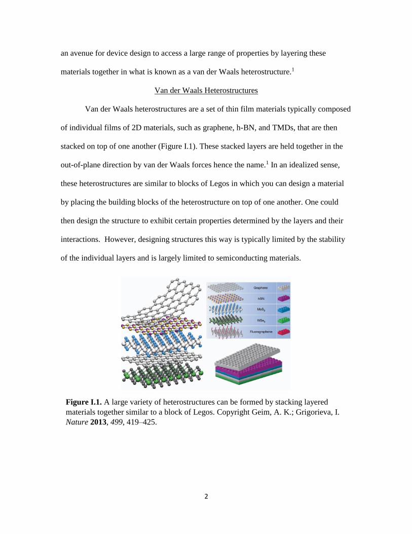
Van der Waals Heterostructures
Van der Waals heterostructures are a set of thin film materials typically composed
of individual films of 2D materials, such as graphene, h-BN, and TMDs, that are then
stacked on top of one another (Figure I.1). These stacked layers are held together in the
out-of-plane direction by van der Waals forces hence the name.1 In an idealized sense,
these heterostructures are similar to blocks of Legos in which you can design a material
by placing the building blocks of the heterostructure on top of one another. One could
then design the structure to exhibit certain properties determined by the layers and their
interactions. However, designing structures this way is typically limited by the stability
of the individual layers and is largely limited to semiconducting materials.
Figure I.1. A large variety of heterostructures can be formed by stacking layered
materials together similar to a block of Legos. Copyright Geim, A. K.; Grigorieva, I.
Nature 2013, 499, 419–425.

3
Misfit Layered Compounds and Ferecrystals: Close cousins to VDWs Heterostructures
Misfit layered compounds (MLCs) are natural heterostructures of the form MTX3
and were initially thought to be ternary compounds until they were discovered to have
more complex structures, through the use of single crystal X-ray diffraction and electron
microscopy.5 MLCs are actually composed of two types of layers. A distorted rock-salt,
MX, with half the thickness of the cell edge of a face centered NaCl, and a transition
metal dichalcogenide trilayer (TX2 or X-T-X). These compounds have the general
formula [(MX)1+δ]m(TX2)n where M is Sn, Pb, Bi, Sb, or a rare earth metal, T is Ti, V,
Nb, Cr, or Ta, and X is S or Se.5–20 Compounds of this type contain m layers of rock-salt
and n layers of dichalcogenide. The c-axis is defined to be normal to the constituent
layers and the name “misfit layered” compounds stems from the incommensurate a-
lattice parameter that forms between layers. This mismatch in the a-lattice is described
by the 1+δ term and can be seen in Figure I.2.
MLCs are synthesized using typical high temperature synthetic routes are limited
to the thermodynamic products of the synthesis.5 This limitation restricts values of m and
n with most common values being m = n = 1 or m = 1 and n = 2.5,21–30 There have been
Figure I.2. Misfit layered compounds are formed with two layered materials that
alternate in the c-direction. The layers distort to form a commensurate b-lattice and
incommensurate a-lattice.
4
reports of compounds with m = 1.5 or 2 and n = 1 and compounds with m = 1 and n =
3.22,31 The electrical properties are typically determined by the more conductive
component of the MLC.5
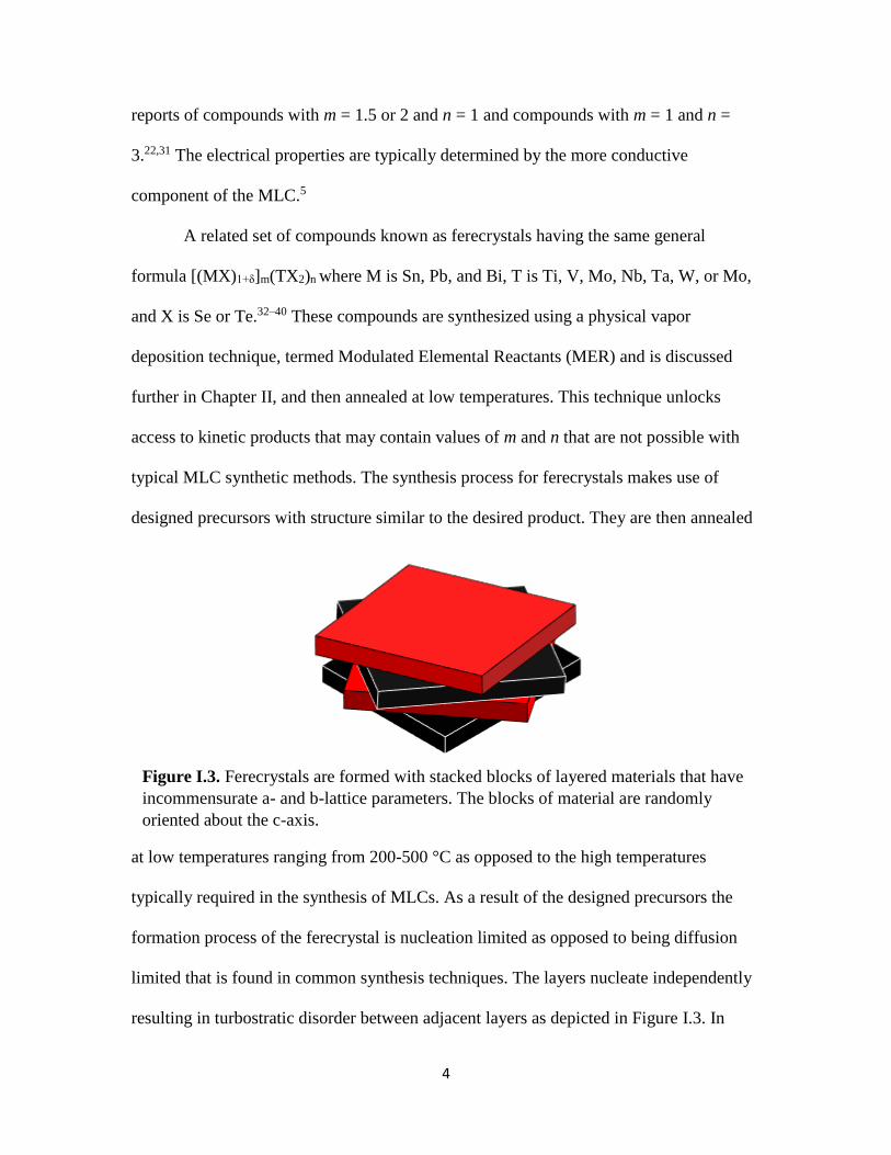
A related set of compounds known as ferecrystals having the same general
formula [(MX)1+δ]m(TX2)n where M is Sn, Pb, and Bi, T is Ti, V, Mo, Nb, Ta, W, or Mo,
and X is Se or Te.32–40 These compounds are synthesized using a physical vapor
deposition technique, termed Modulated Elemental Reactants (MER) and is discussed
further in Chapter II, and then annealed at low temperatures. This technique unlocks
access to kinetic products that may contain values of m and n that are not possible with
typical MLC synthetic methods. The synthesis process for ferecrystals makes use of
designed precursors with structure similar to the desired product. They are then annealed
at low temperatures ranging from 200-500 °C as opposed to the high temperatures
typically required in the synthesis of MLCs. As a result of the designed precursors the
formation process of the ferecrystal is nucleation limited as opposed to being diffusion
limited that is found in common synthesis techniques. The layers nucleate independently
resulting in turbostratic disorder between adjacent layers as depicted in Figure I.3. In
Figure I.3. Ferecrystals are formed with stacked blocks of layered materials that have
incommensurate a- and b-lattice parameters. The blocks of material are randomly
oriented about the c-axis.
5
other words, layers within the ferecrystal have incommensurate a- and b-lattice
parameters. This extensive turbostratic disorder is the origin of the term "ferecrystal"
where fere- is derived from the Greek word for "almost."
The technique by which these ferecrystals are prepared, MER, offers the kinetic
control that the synthetic method of MLCs cannot and provides a way to isolate a
monolayer of a variety of metallic films that is not yet achieved by typical van der Waals
heterostructures.34,39,41,42 The ability to control the values of m and n allows for a
systematic approach to be performed in order to better understand material properties that
may vary as a function of layer thickness.
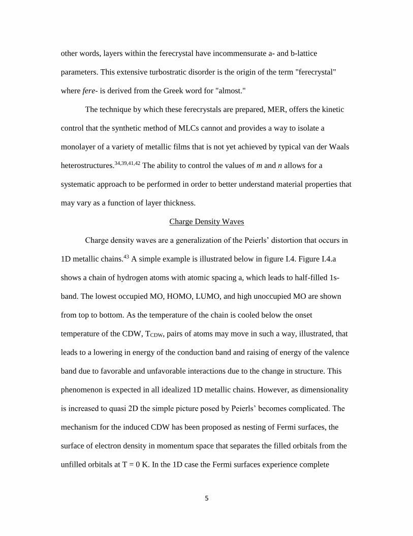
Charge Density Waves
Charge density waves are a generalization of the Peierls’ distortion that occurs in
1D metallic chains.43 A simple example is illustrated below in figure I.4. Figure I.4.a
shows a chain of hydrogen atoms with atomic spacing a, which leads to half-filled 1s-
band. The lowest occupied MO, HOMO, LUMO, and high unoccupied MO are shown
from top to bottom. As the temperature of the chain is cooled below the onset
temperature of the CDW, TCDW, pairs of atoms may move in such a way, illustrated, that
leads to a lowering in energy of the conduction band and raising of energy of the valence
band due to favorable and unfavorable interactions due to the change in structure. This
phenomenon is expected in all idealized 1D metallic chains. However, as dimensionality
is increased to quasi 2D the simple picture posed by Peierls’ becomes complicated. The
mechanism for the induced CDW has been proposed as nesting of Fermi surfaces, the
surface of electron density in momentum space that separates the filled orbitals from the
unfilled orbitals at T = 0 K. In the 1D case the Fermi surfaces experience complete

6
nesting while in the 2D case the Fermi surface becomes more complicated and may only
experience partial nesting and becomes much less common. This phenomenon has been
seen in two dimensional sheets of atoms and is common in metallic transition metal
dichalcogenides, such as, TiSe2, TaSe2, NbSe2, and VSe2.44–49 This nesting is even more
complicated in three dimensions, and as a consequence, less likely to occur. In other
words, in order for a CDW to occur the energetic gain by opening a band gap must
overcome the energetic cost of distorting the lattice. This particular condition is
complicated when you increase the number of interacting atoms.
Charge density waves are of particular interest due to the possibility of inducing
superconductivity due to the modulation of the charge.43 By inducing a voltage across the
chain the atoms may react by oscillating and thereby moving the modulated charge as
seen above in Figure I.4.b. A current issue that arises is the pinning of the charge density
wave due to impurities that are present within the crystal. A simple picture of this
Figure I.4. (a) In a 1-dimensional chain of hydrogen atoms the half-filled s band can
split decreasing the bond distance between atoms to form a unit cell with distance 2a.
(b) The hydrogen atoms can oscillate to induce charge movement.
7
phenomenon is a marble (charge carrier) on a corrugated sheet of metal (lattice). The
depth of the corrugation corresponds to the magnitude of the pinning and increased
defects, while the tilt of the sheet of metal corresponds to the applied voltage. A
consequence of this interaction is a non-linear conduction in response to an applied
electric field.43 An example being the marble interacting with the corrugation of the metal
as it rolls along the surface.
In order to fully realize the use of CDW materials in devices it is imperative that
we expand our understanding of the CDW transition and particularly how it behaves as
the thickness of the CDW material is reduced. In other words, how does the CDW change
as we approach the monolayer limit as opposed to the bulk limit? This question has been
explored previously by determining how TCDW is affected as the monolayer limit
approached. In mechanically exfoliated TiSe2 the onset temperature of the CDW
transition is increased as the thickness of the exfoliated film is decreased.49 In a similar
study of TaSe2 opposing results were reported. As the thickness of exfoliated flakes
decreased the onset temperature also decreased.48 Two studies were performed on VSe2
each showing opposing results likely due to the different exfoliation methods the two
studies performed.50,47 In all four studies mentioned above the monolayer limit was never
achieved and was limited to about 4 trilayers in VSe2 exfoliated films. Additionally
precise control of thickness was not achieved. As mentioned above, the MER technique
for growing ferecrystalline compounds allows for precise control of thickness and
therefore offers a systematic approach to exploring the role of thickness in the CDW
formation. The model system discussed in this thesis is VSe2 containing ferecrystals,
[(MX)1+δ]m(VSe2)n.

8
VSe2 and its Ferecrystals
VSe2 is a layered transmission metal dichalcogenide composed of a Se-V-Se
trilayer (Figure I.5). It has a 1T-CdI2 type trigonal structure with octahedrally coordinated
V. Bulk VSe2 was shown by Bayard et al. to have a resistivity anomaly at 80 K along
with an negative Hall coefficient that increases in magnitude by a factor of 4 at the same
temperature.51 The nature of this behavior has been attributed to a charge density wave
transition.
As mentioned above, later work produced conflicting results as to how TCDW is
affected by the thickness of VSe2 exfoliated flakes. Early work on [(SnSe)1+δ]m(VSe2)n
ferecrystals sought to further explore the nature of the CDW found VSe2. Atkins et. al.
was the first to produce and publish work on ferecrystalline (SnSe)1.15VSe2 showing an
enhanced CDW around 115 K with a positive Hall coefficient that concomitantly
increases in magnitude at the same temperature.34 This increase in Hall coefficient is
indicative of a decrease in carrier concentration indicative of a CDW transition. Further
Figure I.5. An atomic layer of V atoms sandwiched by atomic layers of Se atoms
from a single layer of VSe2. These VSe2 layers stack to form bulk VSe2.

9
work on (SnSe)1+δ(VSe2)n for n = 1-4 was published by Falmbigl et. al.35 It was shown
that for n = 2-3 the electrical behavior is very different compared to n = 1. Resistivity for
n = 4 was not reported in this study. The change in resistivity was attributed to an
increase in dimensionality as the n = 1 system is quasi two-dimensional while values of
n > 1 are three-dimensional. Higher values of n showed bulk like resistivity behavior. In
all systems the room temperature Hall coefficient was positive while for n > 1 there was a
change in sign below 50 K likely due to the breakdown of single-band model typically
used to determine carrier concentration from the Hall coefficient The behavior of the Hall
coefficient in (SnSe)1+δ(VSe2)n is likely due to charge transfer from the SnSe to the VSe2
layer with additional affects from the n value. This work leads to the intuitive question as
to how charge transfer affects the CDW in VSe2 and if charge transfer can be reduced,
enhanced, or completely stopped by material design using the MER method detailed in
Chapter II.
Dissertation Overview
This dissertation explores the synthesis and structural and electrical properties of
VSe2 containing heterostructures. Chapter II outlines the synthetic method, known as
modulated elemental reactants, that is used to target and synthesize multi-constituent
heterostructures. Additionally, there is a thorough discussion of the techniques used to
characterize the structural and electrical properties of the designed films. Three sets of
kinetically stable VSe2 heterostructures are discussed in Chapters III to V. Chapter III
seeks to explore the uniqueness of the charge density wave that was previously observed
in (SnSe)1.15VSe2 by preparing a set of (PbSe)1+δ(VSe2)n for n = 1 – 3. Chapter IV
explores the effect of charge transfer on the charge density wave by characterizing

10
(BiSe)1+δVSe2. Chapter V replaces the rocksalt layer with 1T-SnSe2 forming
(SnSe2)1+δVSe2 in an attempt to determine the role of structural interface on the charge
density wave. These chapters are presented individually to explore the effects of
interlayer interactions on the charge density wave observed in VSe2 containing
heterostructures. Chapter VI provides concluding remarks. The work presented within
this dissertation was made possible through the help and joint effort of many individuals.
Chapter I and II were prepared with the assistance of my thesis advisor David C.
Johnson. Chapter III is published and co-authored with Matthias Falmbigl, Matti B.
Alemayehu, Marco Esters, Suzannah R. Wood, and David C. Johnson. Chapter IV is
published and co-authored with Michael Nellist, Jeffrey Ditto, Matthias Falmbigl, and
David C. Johnson. Chapter V is in preparation for publication and the co-authors: Erik
Hadland, James Sadighian, and David C. Johnson.

11
CHAPTER II
EXPERIMENTAL PROCEDURES
Authorship Statement
My advisor, David C. Johnson, was consulted in the preparation of this chapter.
Modulated Elemental Reactants Technique
The modulated elemental reactant (MER) technique was developed in the Dave
Johnson laboratory in the 1990s. The MER technique provides access to kinetic materials
that are not accessible via typical solid state synthesis techniques. Precursors are designed
to closely match the nanoarchitecture of the desired final product. These “designed”
precursors are nucleation limited rather than diffusion limited as in typical synthetic
techniques. They are annealed at low temperature to enable nucleation of the material.1
Precursors were prepared in a custom-built physical vapor deposition chamber
pictured below (Figure II.1).2 The chamber uses 3 3-kW Thermionic electron beam guns
to evaporate Sn, V, Pb, and Bi and a Knudsen effusion cell to evaporate Se. Elemental
vapor is deposited on a (100) oriented Si substrate and rate of deposition is controlled by
INFICON Xtal quartz crystal microbalances (QCMs). QCMs are approximately 25 cm
above the elemental sources. Elemental sources of Sn, V (99.8%), Se (99.999%), Pb
(99.995%), and Bi are obtained from Alfa Aesar. The refractory metal, vanadium, is first
melted in an arc melter in a He atmosphere prior to deposition. Sn, Pb, and Bi are placed
in a graphite crucible prior to evaporation. V, Pb, and Bi are deposited at a rate of 0.04
nm/s, Sn at 0.03 nm/s, and Se at 0.05 nm/s. A QCM tooling factor of 68 is used for Se
and 64 is used for all other elements to account for the spatial difference of the QCM and
the Si substrate. A pre-programmed LabView controls a carousel to move substrates to
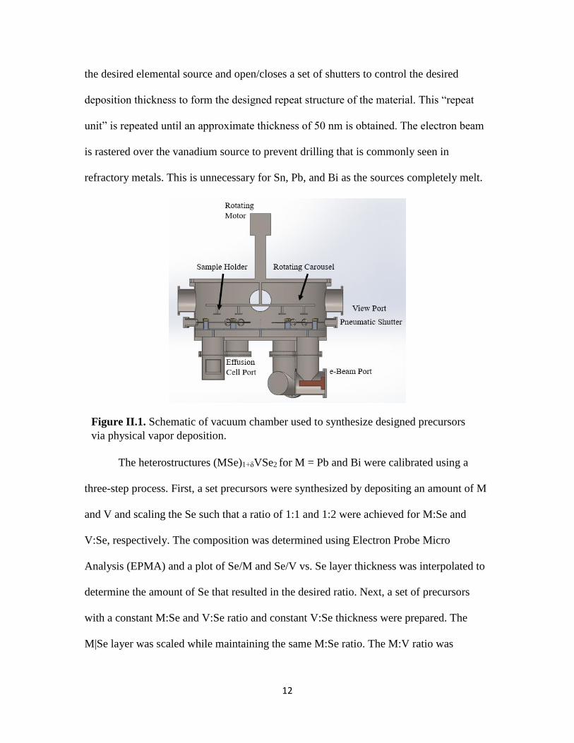
12
the desired elemental source and open/closes a set of shutters to control the desired
deposition thickness to form the designed repeat structure of the material. This “repeat
unit” is repeated until an approximate thickness of 50 nm is obtained. The electron beam
is rastered over the vanadium source to prevent drilling that is commonly seen in
refractory metals. This is unnecessary for Sn, Pb, and Bi as the sources completely melt.
The heterostructures (MSe)1+δVSe2 for M = Pb and Bi were calibrated using a
three-step process. First, a set precursors were synthesized by depositing an amount of M
and V and scaling the Se such that a ratio of 1:1 and 1:2 were achieved for M:Se and
V:Se, respectively. The composition was determined using Electron Probe Micro
Analysis (EPMA) and a plot of Se/M and Se/V vs. Se layer thickness was interpolated to
determine the amount of Se that resulted in the desired ratio. Next, a set of precursors
with a constant M:Se and V:Se ratio and constant V:Se thickness were prepared. The
M|Se layer was scaled while maintaining the same M:Se ratio. The M:V ratio was
Figure II.1. Schematic of vacuum chamber used to synthesize designed precursors
via physical vapor deposition.

13
monitored as function of M|Se deposited to determine the parameters that yielded a ratio
for M:V equal to the theoretical 1+δ misfit parameter. Finally, a set of precursors were
prepared with constant M:Se, V:Se, and M|Se:V|Se ratios and scaled total thickness in
order to achieve the required thickness to form a complete rocksalt MSe bilayer and
trigonal VSe2 trilayer. An excess of Se was deposited in each layer to compensate for Se
loss that occurs during the annealing process.
(MSe)1+δVSe2 (M = Pb and Bi) precursors were annealed at varying temperatures
and time in order to determine the ideal annealing conditions for heterostructure
formation. This “annealing study” was performed on a hotplate in an N2 atmosphere with
<0.5ppm O2. The ideal annealing conditions were ones that maximized the intensity and
minimized the full width at half maximum of 00l reflections.
The heterostructure (SnSe2)1+δVSe2 was calibrated by targeting the ideal counts
per second (cps) for each element as determined by X-ray Fluorescence (further details
for XRF can be found in section II.4). A precursor with an arbitrary amount of Sn, Se and
V is prepared and composition is measured using XRF. The deposition parameters for
each element are scaled by the ratio of ideal kcps:measured kcps and a new precursor is
prepared with the ideal deposition parameters, which yields a precursor with ideal kcps.
(SnSe2)1+δVSe2 was first annealed on a hotplate in an N2 atmosphere with <0.5
ppm O2. The “pre-annealed” precursor was then sealed in an outgassed Pyrex ampule
with bulk SnSe2 at ~10-6 torr. An annealing study was performed to determine the ideal
temperature and time required to minimize intensity and full width at half maximum for
00l reflections while also producing hk0 reflections that correspond to trigonal SnSe2 and
trigonal VSe2.
14
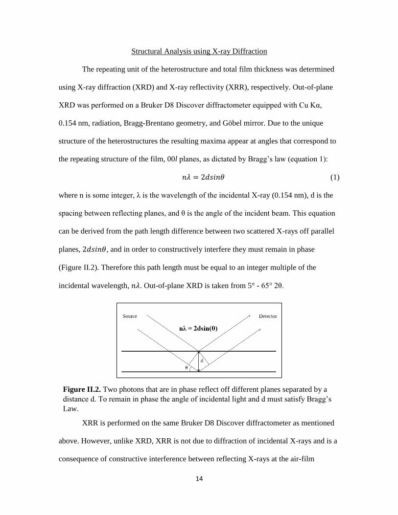
Structural Analysis using X-ray Diffraction
The repeating unit of the heterostructure and total film thickness was determined
using X-ray diffraction (XRD) and X-ray reflectivity (XRR), respectively. Out-of-plane
XRD was performed on a Bruker D8 Discover diffractometer equipped with Cu Kα,
0.154 nm, radiation, Bragg-Brentano geometry, and Göbel mirror. Due to the unique
structure of the heterostructures the resulting maxima appear at angles that correspond to
the repeating structure of the film, 00l planes, as dictated by Bragg’s law (equation 1):
𝑛𝜆 = 2𝑑𝑠𝑖𝑛𝜃 (1)
where n is some integer, λ is the wavelength of the incidental X-ray (0.154 nm), d is the
spacing between reflecting planes, and θ is the angle of the incident beam. This equation
can be derived from the path length difference between two scattered X-rays off parallel
planes, 2𝑑𝑠𝑖𝑛𝜃, and in order to constructively interfere they must remain in phase
(Figure II.2). Therefore this path length must be equal to an integer multiple of the
incidental wavelength, 𝑛𝜆. Out-of-plane XRD is taken from 5° - 65° 2θ.
XRR is performed on the same Bruker D8 Discover diffractometer as mentioned
above. However, unlike XRD, XRR is not due to diffraction of incidental X-rays and is a
consequence of constructive interference between reflecting X-rays at the air-film
Figure II.2. Two photons that are in phase reflect off different planes separated by a
distance d. To remain in phase the angle of incidental light and d must satisfy Bragg’s
Law.

15
interface and film-substrate interface. The resulting peaks appear at angles dictated by the
modified Bragg’s law and are termed Kiessig fringes.3
𝑛𝜆 = 2𝑑(𝑠𝑖𝑛2𝜃 − 𝑠𝑖𝑛2𝜃𝑐)1
2 (2)
The modified Bragg’s law accounts for the extra distance traveled by the penetrating X-
rays due to the critical angle, 𝜃𝑐. It is important to note that if the film is more optically
dense than the substrate a phase shift of π is observed and 𝑛 becomes 𝑛 + 1
2. XRR is
performed from 0° - 11° 2θ.
In-plane lattice parameters of the individual layers are determined using in-plane
XRD (hk0 XRD) (Figure II.3). In-plane XRD is performed on a Rigaku SmartLab
equipped with Cu Kα radiation and at the Advance Photon Source at Argonne National
Laboratory. Due to the structure of the heterostructures only hk0 reflections are observed,
which allows for determination of in-plane lattice parameters.4
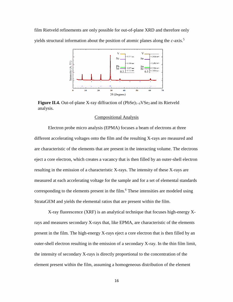
Rietveld Refinement
Rietveld analysis is performed on the off-specular X-ray diffraction patterns to
further determine the structure of the heterostructure (Figure II.4). A Rietveld refinement
employs a least squares algorithm to obtain a best fit between a structural model and an
X-ray diffraction pattern. In order for the algorithm to converge a model that closely
approximates the actual structure of the film is required. Due to the textured nature of the
Figure II.3. In-plane X-ray diffraction of (PbSe)1+δVSe2.
16
film Rietveld refinements are only possible for out-of-plane XRD and therefore only
yields structural information about the position of atomic planes along the c-axis.5
Compositional Analysis
Electron probe micro analysis (EPMA) focuses a beam of electrons at three
different accelerating voltages onto the film and the resulting X-rays are measured and
are characteristic of the elements that are present in the interacting volume. The electrons
eject a core electron, which creates a vacancy that is then filled by an outer-shell electron
resulting in the emission of a characteristic X-rays. The intensity of these X-rays are
measured at each accelerating voltage for the sample and for a set of elemental standards
corresponding to the elements present in the film.6 These intensities are modeled using
StrataGEM and yields the elemental ratios that are present within the film.
X-ray fluorescence (XRF) is an analytical technique that focuses high-energy X-
rays and measures secondary X-rays that, like EPMA, are characteristic of the elements
present in the film. The high-energy X-rays eject a core electron that is then filled by an
outer-shell electron resulting in the emission of a secondary X-ray. In the thin film limit,
the intensity of secondary X-rays is directly proportional to the concentration of the
element present within the film, assuming a homogeneous distribution of the element
Figure II.4. Out-of-plane X-ray diffraction of (PbSe)1+δVSe2 and its Rietveld
analysis.
17
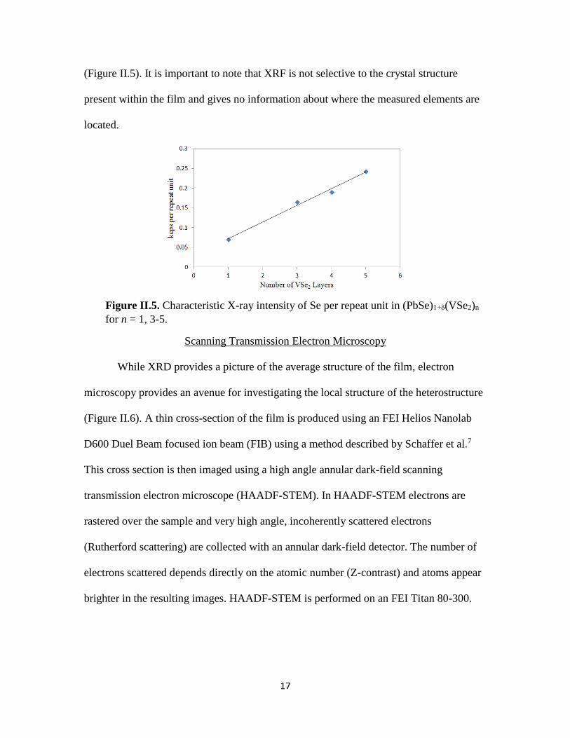
(Figure II.5). It is important to note that XRF is not selective to the crystal structure
present within the film and gives no information about where the measured elements are
located.
Scanning Transmission Electron Microscopy
While XRD provides a picture of the average structure of the film, electron
microscopy provides an avenue for investigating the local structure of the heterostructure
(Figure II.6). A thin cross-section of the film is produced using an FEI Helios Nanolab
D600 Duel Beam focused ion beam (FIB) using a method described by Schaffer et al.7
This cross section is then imaged using a high angle annular dark-field scanning
transmission electron microscope (HAADF-STEM). In HAADF-STEM electrons are
rastered over the sample and very high angle, incoherently scattered electrons
(Rutherford scattering) are collected with an annular dark-field detector. The number of
electrons scattered depends directly on the atomic number (Z-contrast) and atoms appear
brighter in the resulting images. HAADF-STEM is performed on an FEI Titan 80-300.
Figure II.5. Characteristic X-ray intensity of Se per repeat unit in (PbSe)1+δ(VSe2)n
for n = 1, 3-5.

18
Transport Property Measurements
In-plane resistivity and Hall effect measurements were taken on a custom-built
instrument using the van der Pauw technique. 8 The van der Pauw method allows for the
electrical characterization of arbitrary shaped lamellae, assuming the lamella meets three
criteria:
1. The lamellae is approximately two-dimensional,
2. The lamellae is free of isolated pin-holes,
3. The electrical contacts are an order of magnitude smaller in area than the
lamellae, and ideally as small as possible.
For our purposes, a cross-shaped geometry was used in order to allow for uniform current
(Figure II.7). Samples are deposited through a cross-shaped shadow mask and collected
on a fused silica substrate. Copper leads are contacted to the sample with indium at each
point of the cross. For resistivity measurements, voltage leads are contacted at adjacent
points along with current leads. A known current is applied and the resulting voltage is
Figure II.6. HAADF-STEM images of (PbSe)1+δVSe2 shows alternating layers of
PbSe and VSe2 with turbostratic disorder.

19
measured. This measurement is conducted in all 8 possible configurations allowing for an
average resistivity to be calculated:
𝜌 = 𝜋𝑑
ln 2
𝑅𝐴𝐵,𝐶𝐷+𝑅𝐵𝐶,𝐷𝐴
2𝑓 (3)
Where d is the film thickness, R is the sheet resistance, and f is the symmetry constant for
the cross pattern.
Hall effect measurements place voltage leads at opposite corners of the cross and
the current at the remaining two corners (Figure II.8). A current is sourced across the two
leads and a magnetic field is applied in the out-of-plane direction, the moving electrons
experience a Lorentz force. The direction of this force is governed by the “right-hand
rule” for electrons and the “left-hand rule” for holes. This induces a separation of
negatively charged and positively charges particles. This induced voltage is then
measured. The Hall coefficient is then calculated using the Hall voltage, VH, the applied
current, I, applied magnetic field, B, and the thickness of the film:
𝑅𝐻 = 𝑉𝐵𝑑
𝐼𝐵. (4)
Under the assumption that the conducting band in the film is singular and rigid then a
carrier concentration can be calculated:
Figure II.7. Two of the eight possible lead combinations used in order to measure in-
plane electrical resistivity.

20
𝑉𝐻 = 𝐼𝐵
𝑛𝑒𝑑 (5)
where n is the carrier concentration and e is the elemental charge of the carrier.
Bridge
The technique explained throughout this chapter are employed throughout the
remainder of this dissertation. In order to understand what follows it is imperative that
one understands the techniques by which these materials are analyzed. These techniques
are used to provide insight into the structure of these of heterostructures and their
electrical behavior.
Figure II.8. Two of the possible four combinations used to measure the Hall
coefficient.

21
CHAPTER III
CHARGE DENSITY WAVE TRANSITION IN (PBSE)1+Δ(VSE2)N
WITH N = 1, 2, AND 3
Authorship Statement
This work appeared in Chemistry of Materials in 2017, volume 29, issue 13,
pages 5646 – 5653. I am the primary author of this work. Matti B. Alemayehu and
Matthias Falmbigl assisted with sample synthesis. Matthias Falmbigl also assisted with
diffraction analysis. Marco Esters performed DFT calculations. Suzannah R. Wood
assisted in figure generation. David C. Johnson is my advisor and consulted in
preparation of this manuscript. Reprinted with permission from Charge Density Wave
Transition in (PbSe)1+δ(VSe2)n Compounds with n = 1, 2, and 3 Omar K. Hite, Matthias
Falmbigl, Matti B. Alemayehu, Marco Esters, Suzannah R. Wood, and David C. Johnson
Chemistry of Materials 2017 29 (13), 5646-5653. Copyright 2017 American Chemical
Society.
Introduction
The isolation of graphene1 and the discovery that its properties differ from those
of bulk graphite has lead to a surge of research on single layer and very thin layers of
quasi-two-dimensional systems such as h-boron nitride (h-BN)2,3 and transition metal
dichalcogenides4 and their heterostructures5 in a search for emergent properties not
present in the bulk constituents. For MoS2 a transition was observed from an indirect to a
direct band gap semiconductor as the materials dimensions are reduced from bulk to a
single sheet.6 It has been shown computationally that SnS, SnSe, GeS, and GeSe have
increased band gaps as the number of layers is reduced from the bulk to monolayer.7 A

22
similar trend in band gaps is seen for h-BN, where the bulk 4.0 eV band gap increases to
a 4.6 eV band gap in the monolayer.8 Emergent properties have also been observed in
heterostructures,9–12 including ultrafast charge transfer in MoS2/WS2 consistent with a
type II band alignment having spatially direct absorption, but spatially indirect
emission.13 Other examples include long-lived interlayer excitons in a MoSe2-WSe2
heterostructure with experimentally observed type II band alignment,14 and epitaxial
single-layers of MoS2 on a Au(111) surface showing a dramatic change in their band
structure around the center of the Brillouin zone.15
The majority of the systems being investigated are semiconducting because
isolation of single sheets of metallic systems has been challenging as they are not stable
in air.11 There are a number of interesting properties in metallic systems, however, that
are being explored as a function of thickness towards the 2D limit, including
superconductivity, and charge density waves (CDW). It has been demonstrated that the
onset temperature of superconductivity in 2H-NbSe2 decreases as the number of NbSe2
layers is decreased.16–18 Studies on mechanically exfoliated TiSe2 have shown that as
thickness of the exfoliated film is decreased the onset temperature of the CDW is
increased.26 Others have shown that the onset temperature of the CDW in TaSe2 is
decreased as the thickness of the mechanically exfoliated film is decreased.27 It was
shown both computationally and experimentally, that the ferromagnetism of VS2 is
enhanced as the VS2 approaches the monolayer limit.19,20 VSe2 exhibits a CDW transition
in the bulk21 but there is disagreement on how this CDW changes as the number of VSe2
layers are reduced in this n-type metal.22–25 The onset of the CDW in thin layers of VSe2
prepared via liquid exfoliation transitions from 100 K21 in the bulk single crystal to 135 K
23
as thickness is reduced to 4-8 trilayers of VSe2.22 An opposite trend has been reported for
micromechanically exfoliated nanoflakes, however, where the onset temperature
decreases to 81 K at the lowest thickness measured, 11.6 nm.23 The thin nanoflakes are n-
type conductors, as is bulk VSe2, but the carrier concentration increases as the nanoflake
thickness is decreased. These exfoliation techniques were not able to precisely control the
thickness of the VSe2 flakes nor were they able to reach the monolayer limit. Studies of
[(SnSe)1.15]m(VSe2)n prepared by annealing designed precursors have shown that
compounds with a single layer of VSe2 separated by m layers of SnSe are p-type metals
with a CDW that depends on the thickness of SnSe and exhibit a dramatic change in
electrical resistivity and charge carrier concentration at the CDW transition
temperature.28 In contrast, increasing the VSe2 layer thickness to two or more layers
results in low temperature n-type metals and the suppression of the pronounced effect in
transport properties at the CDW transition temperature similar to bulk VSe2.25 These
compounds grown at low temperatures from designed precursors have been called
ferecrystals, from the Latin root fere- meaning “almost”, due to their extensive
turbostratic disorder. The influence of surface contaminations and/or the substrate on the
charge density wave transition has not been explored or discussed in the literature.
In order to explore the impact of neighboring layers on the CDW of VSe2
heterostructures, we replaced SnSe with the isovalent PbSe in a sequence of
(PbSe)1+δ(VSe2)n compounds. The compounds were prepared using modulated elemental
reactant precursors and electrical properties were measured as a function of temperature.
Diffraction data is consistent with n layers of VSe2 separating a single rock salt structured
PbSe layer. The n = 1 ferecrystal is metallic with a positive Hall coefficient indicative of
24
p-type conduction, while for the n = 2 and 3 compounds, the Hall coefficient switches
sign, indicating a change of the majority carriers to electrons equivalent to bulk VSe2.21
Both the resistivity and Hall coefficient of the n = 1 compound increase as the
temperature is lowered below 100 K, becoming a factor of 3.7 and 8 higher, respectively,
by 20 K. This anomaly is very similar to the CDW transition observed in
([SnSe]1.15)mVSe2 compounds. The temperature dependencies of the resistivity and Hall
coefficient of the n = 2 and 3 compounds are very similar to bulk VSe2. There is a change
in the slope of the resistivity and the Hall coefficient as a function of temperature at
100 K, suggesting that a CDW similar to the bulk occurs if there is more than one VSe2
layer. The different sign of the Hall coefficient and large changes in resistivity and Hall
coefficient indicates, the electronic structure of (PbSe)1+δVSe2 with a single VSe2 layer is
distinctly different than heterostructures with thicker VSe2 layers. The changes in
properties when PbSe replaces SnSe, although only an isovalent substitution, indicates
that the interactions between constituents can be used to tune the electrical properties of
heterostructures.
Experimental Methods
The ferecrystalline compounds, (PbSe)1+δ(VSe2)n where 1 ≤ n ≤ 3, were
synthesized using the modulated elemental reactants (MER) technique.29 Precursors were
prepared by sequentially evaporating elemental sources of Pb (99.995%, Alfa Aesar), V
(99.8%, Alfa Aesar), and Se (99.999%, Alfa Aesar) on (100) oriented Si wafers in
specific sequences for each compound in a custom built high-vacuum physical vapor
deposition chamber, details provided elsewhere.29 Precursors were annealed at 250 °C for
1 hour in a N2 glove box with a concentration of oxygen below 0.6 ppm. Methods used to

25
determine the optimal annealing temperatures for converting the precursors into the
desired product are described in the literature.24
Specular X-ray diffraction (XRD) was performed to determine the c-axis lattice
parameter of the (PbSe)1+δ(VSe2)n compounds on a Bruker D8 Discover diffractometer
equipped with Cu Kα radiation (λ = 0.15418 nm), Göbel mirrors, and Bragg-Brentano θ-
2θ optics geometry. In-plane XRD of the n = 1 and 3 compounds were taken at the
Advanced Photon Source, Argonne National Laboratories (BM 33-C)(λ = 0.12653 nm).
In-plane XRD of the n = 2 compound was done on a Rigaku SmartLab diffractometer
equipped with Cu Kα radiation.
Compositional analysis was performed with electron probe micro-analysis
(EPMA) on a Cameca SX-100. Accelerating voltages of 7.5, 13, and 18 keV were used
and overall composition was calculated as a function of the three accelerating voltages
using the technique for thin films developed by Donovan et al.30
Samples were prepared for High-angle Annular Dark-field Scanning
Transmission Electron Microscopy (HAADF-STEM) on a FEI Helios 600 dual-beam
using a technique described by Schaffer et al.31 HAADF-STEM was taken on a FEI Titan
80-300 FEG-TEM at the Center for Advanced Materials Characterization in Oregon
(CAMCOR).
Electrical resistivity and Hall measurements were determined using the van der
Pauw technique32 in a temperature range of 20 - 295 K. Samples were prepared on fused
Quartz crystal slides in a 1 cm × 1 cm cross geometry. Further details on how
temperature-dependent resistivity and Hall measurements were conducted are described
elsewhere.33
26
Results and Discussion
Precursors for each of the compounds (PbSe)1+δ(VSe2)n with n = 1 - 3 were
prepared by depositing sequences of elemental layers where the elemental Pb|Se and V|Se
bilayers were calibrated to match the composition of the desired product such that each
Pb|Se bilayer formed two (001) planes of rock salt structured PbSe and each V|Se bilayer
formed a single Se-V-Se dichalcogenide structured trilayer. The calibration was a three-
step process. The composition of the Pb|Se and V|Se bilayers were calibrated by
preparing a set of samples with a fixed metal thickness and varying thicknesses of Se, and
determining the composition with EPMA. The resulting graphs of Se:Pb and Se:V ratio
versus Se layer thickness were interpolated to obtain the ratio of thicknesses that resulted
in the respective desired compositions. To determine the thickness ratio between the Pb
and V layers to obtain the targeted misfit parameter of 1.11, a set of samples were
prepared by depositing Pb|Se|V|Se sequences where the thickness of the Pb|Se bilayer at
the previously determined Pb/Se thickness ratio was scaled while holding the thickness
and thickness ratio of the V|Se bilayer constant. The change in composition as a function
of the thickness of the Pb|Se bilayer was interpolated to find the thickness required to
obtain the desired misfit parameter. The last step was to hold the Pb|Se, V|Se and
Pb|Se/V|Se ratios constant while scaling the total thickness, using the quality of the
resulting annealed sample diffraction patterns to determine the thickness such that each
Pb|Se bilayer forms two (001) planes of rock salt structured PbSe and the V|Se layer
forms a single Se-V-Se dichalcogenide structured trilayer. X-ray diffraction (XRD) scans
were taken on the annealed precursors in order to determine the total thickness that yields
27
maximum peak intensity and minimum peak FWHM in the resulting product, as
described previously by Atkins et al.34
Sequences with the nanoarchitecture of the desired products, for example the
sequence of layers Pb|Se-V|Se-V|Se for (PbSe)1+δ(VSe2)2, were repeatedly deposited until
the desired total sample thickness of about 45 nm was reached. These precursors were
annealed at 250 °C to self-assembly of the targeted products. This temperature was
determined using the approach of Atkins et al.34 Figure III.1 shows the specular XRD
patterns of the n = 1 - 3 compounds. Each peak can be indexed to a 00l reflection of the
(PbSe)1+δ(VSe2)n compounds indicating crystallographically aligned layers with the c-
axis perpendicular to the substrate. Using Bragg’s Law, the c-axis lattice parameters were
determined to be 1.225(1) nm, 1.835(3) nm, and 2.445(4) nm for n = 1, 2, and 3,
respectively. The change in thickness as n is increased yields the thickness of a VSe2
layer from the slope and the thicknesses of the PbSe layer from the intercept. The PbSe
bilayer thickness of 0.617(5) nm is slightly thicker than the 0.607-0.612 nm found in a
series of [(PbSe)1.14]m(NbSe2)n compounds33 and the 0.61(1) nm found for the PbSe
bilayer thickness in (PbSe)1+δ(TiSe2)n ferecrystals.35 The thickness of the VSe2 trilayer is
0.610(2) nm, which is slightly thicker than the 0.596(1) nm reported for the VSe2 sub-unit
in (SnSe)1.15(VSe2)n compounds.13

28
A Rietveld refinement of the n = 1 out-of-plane XRD was performed to determine
relative positions of the atomic planes along the c-axis. Figure III.2 contains the fitted
intensities along with a schematic of the atomic plane positions compared to those
previously determined for (SnSe)1.15VSe2.14 The refinement revealed puckering of the
PbSe layer, which separates the Pb and Se atomic planes from one another by
0.0367(2) nm. This puckering is typical for bilayers of rock salt structured constituents
and has been seen previously in both SnSe and PbSe containing misfit layered
compounds and ferecrystals.25,36 The magnitude of this puckering is within the range
reported previously, 0.020 nm to 0.065 nm, in the relatively few atomic level structures
that have been previously determined.37–43 It is larger than the puckering observed in
(PbSe)1.00MoSe2 (0.025(1) nm) and (PbSe)0.99WSe2 (0.021(1) nm) ferecrystals44 but
smaller than the 0.062(5) nm found in the (PbSe)1.18(TiSe2)2 ferecrystal.45 The extent of
the puckering may be related to the amount of charge transfer between the constituents,
as a negatively charged environment in the dichalcogenide layer would attract the
Figure III.1. X-ray diffraction of (PbSe)1+δ(VSe2)n for n = 1-3 using Cu Kα radiation
(λ = 0.15418 nm). Maxima can be indexed to 00l reflections of the respective
compound, with the appropriate index given the figure for the reflection at the ~29°
2θ. Asterisks (*) indicate substrate or stage reflections.
29
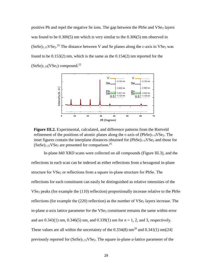
positive Pb and repel the negative Se ions. The gap between the PbSe and VSe2 layers
was found to be 0.300(5) nm which is very similar to the 0.306(5) nm observed in
(SnSe)1.15VSe2.25 The distance between V and Se planes along the c-axis in VSe2 was
found to be 0.153(2) nm, which is the same as the 0.154(2) nm reported for the
(SnSe)1.15(VSe2) compound.25
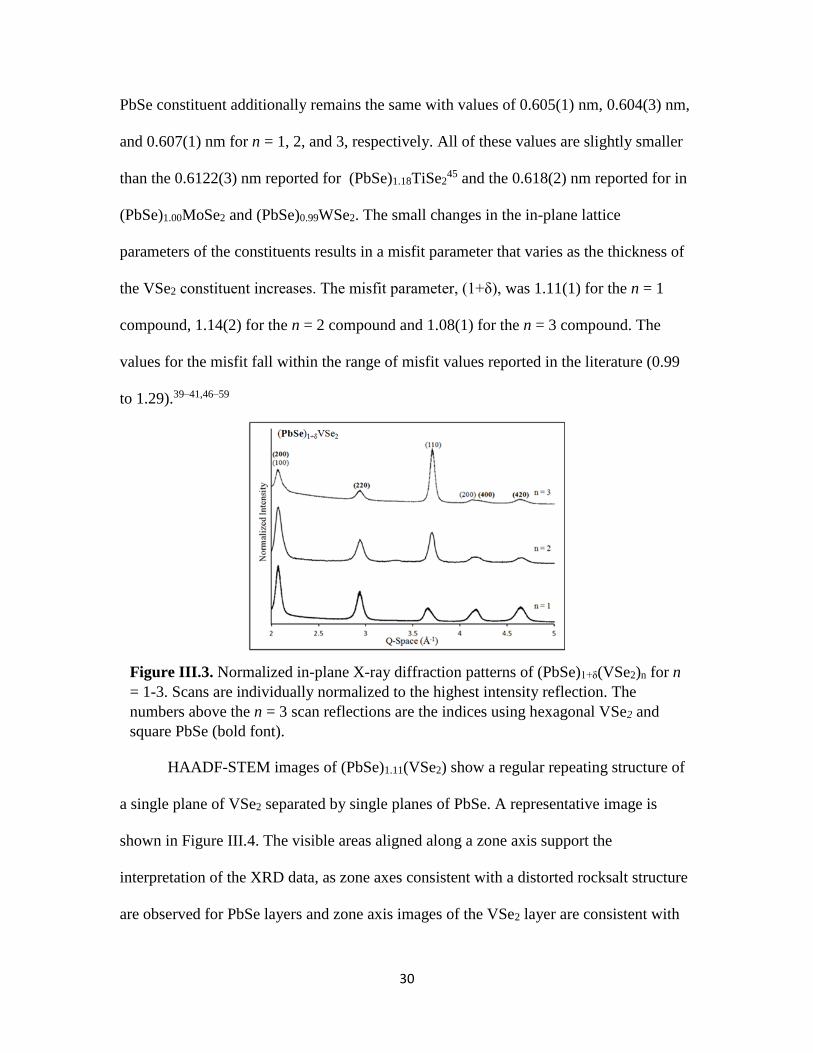
In-plane hk0 XRD scans were collected on all compounds (Figure III.3), and the
reflections in each scan can be indexed as either reflections from a hexagonal in-plane
structure for VSe2 or reflections from a square in-plane structure for PbSe. The
reflections for each constituent can easily be distinguished as relative intensities of the
VSe2 peaks (for example the (110) reflection) proportionally increase relative to the PbSe
reflections (for example the (220) reflection) as the number of VSe2 layers increase. The
in-plane a-axis lattice parameter for the VSe2 constituent remains the same within error
and are 0.343(1) nm, 0.346(5) nm, and 0.339(1) nm for n = 1, 2, and 3, respectively.
These values are all within the uncertainty of the 0.334(8) nm28 and 0.341(1) nm[24]
previously reported for (SnSe)1.15VSe2. The square in-plane a-lattice parameter of the
Figure III.2. Experimental, calculated, and difference patterns from the Rietveld
refinement of the positions of atomic planes along the c-axis of (PbSe)1+δVSe2. The
inset figures contain the interplane distances obtained for (PbSe)1+δVSe2 and those for
(SnSe)1.15VSe2 are presented for comparison.25
30
PbSe constituent additionally remains the same with values of 0.605(1) nm, 0.604(3) nm,
and 0.607(1) nm for n = 1, 2, and 3, respectively. All of these values are slightly smaller
than the 0.6122(3) nm reported for (PbSe)1.18TiSe245 and the 0.618(2) nm reported for in
(PbSe)1.00MoSe2 and (PbSe)0.99WSe2. The small changes in the in-plane lattice
parameters of the constituents results in a misfit parameter that varies as the thickness of
the VSe2 constituent increases. The misfit parameter, (1+δ), was 1.11(1) for the n = 1
compound, 1.14(2) for the n = 2 compound and 1.08(1) for the n = 3 compound. The
values for the misfit fall within the range of misfit values reported in the literature (0.99
to 1.29).39–41,46–59
HAADF-STEM images of (PbSe)1.11(VSe2) show a regular repeating structure of
a single plane of VSe2 separated by single planes of PbSe. A representative image is
shown in Figure III.4. The visible areas aligned along a zone axis support the
interpretation of the XRD data, as zone axes consistent with a distorted rocksalt structure
are observed for PbSe layers and zone axis images of the VSe2 layer are consistent with
Figure III.3. Normalized in-plane X-ray diffraction patterns of (PbSe)1+δ(VSe2)n for n
= 1-3. Scans are individually normalized to the highest intensity reflection. The
numbers above the n = 3 scan reflections are the indices using hexagonal VSe2 and
square PbSe (bold font).

31
octahedral coordination of the vanadium atoms, which are situated between Se planes.
The disorder in the orientation of the layers from layer to layer indicates that there is no
long-range order. This is consistent with the XRD data, which show that there is long
range order due to alternating VSe2 and PbSe layers along (00l), that each layer is
crystalline with distinct (hk0) diffraction from each of the constituents, and that there is
no common in-plane axis between the constituents. The crystalline nature of each of the
constituent layers with lack of long-range order between planes is a consequence of the
mechanism of the self-assembly from the precursor.60
Temperature dependent resistivity measurements were conducted on all samples
and the data is plotted in Figure III.5 along with data previously reported for bulk VSe2.21
The absolute value of the room temperature resistivity and the temperature dependence of
the resistivity above 150 K for all samples indicate that they are metallic. The magnitude
of the resistivity systematically decreases as the percentage of the metallic constituent
VSe2 is increased, which is consistent with conduction occurring primarily through the
VSe2 layer as observed in the analogous (PbSe)1.12(NbSe2)n compounds.33 The
Figure III.4. HAADF-STEM images of (PbSe)1.11VSe2 contain alternating PbSe
bilayers and VSe2 trilayers. The different crystallographic orientations of the PbSe
layers are a result of turbostratic disorder. The expanded image shows a PbSe layer
with [100] crystallographic orientation (top) and a [110] crystallographic orientation
(bottom). The VSe2 layer is consistent with octahedral coordination of V.

32
temperature dependence of the n = 3 sample is similar to that of bulk VSe2, with a
slightly decreased temperature dependence suggesting weaker electron-phonon scattering
compared to bulk VSe2. The temperature dependence of the n = 2 sample shows a further
decrease in the slope, suggesting even weaker electron-phonon scattering. The weaker
electron-phonon scattering reflects the changes in phonon modes and phonon energies as
the VSe2 block is reduced in thickness. The n = 2 and 3 heterostructures both show a
change in slope of the resistivity that is very similar to that seen as a result of a CDW in
bulk VSe2. The temperature dependence of the n = 1 sample is distinctly different than
bulk VSe2 and the n = 2 and 3 heterostructures, with the resistivity abruptly increasing at
approximately 110 K as temperature is lowered. The resistivity ultimately reaches a value
of more than 5 times higher at 20 K than would be extrapolated from the high
temperature behavior. The change in resistivity of (PbSe)1.11VSe2 is very similar to that
reported by Falmbigl et al. for (SnSe)1.15(VSe2),25 which has been attributed to a charge
density wave (CDW) based on resistivity, Hall coefficient and heat capacity
measurements.61 The overall increase in resistivity in the (PbSe)1.11VSe2 compound is
approximately double that of the analogous SnSe compound, indicating that a higher
percentage of the charge carriers are localized and/or that there is a significant difference
in the change of the carrier mobility below the CDW. This may reflect structural
differences at the interface between the constituents (in n = 1 the VSe2 and PbSe layers
alternate and for the other compounds PbSe is separated by 2 or 3 VSe2 layers) or a
different Fermi level caused by a difference in charge transfer between the SnSe
(bulk Eg, 1.38 eV62) or PbSe (bulk Eg, 0.23 eV63) layer and the VSe2 layers. The
difference in charge transfer could be a consequence of the different misfit parameters
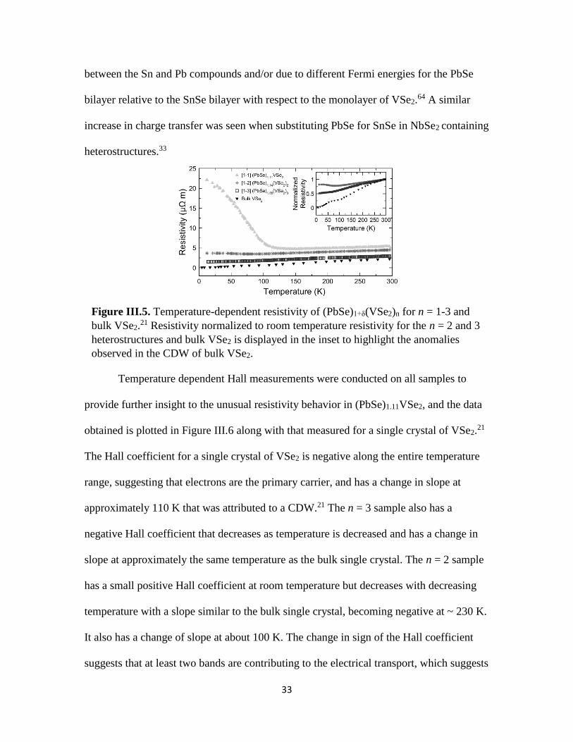
33
between the Sn and Pb compounds and/or due to different Fermi energies for the PbSe
bilayer relative to the SnSe bilayer with respect to the monolayer of VSe2.64 A similar
increase in charge transfer was seen when substituting PbSe for SnSe in NbSe2 containing
heterostructures.33
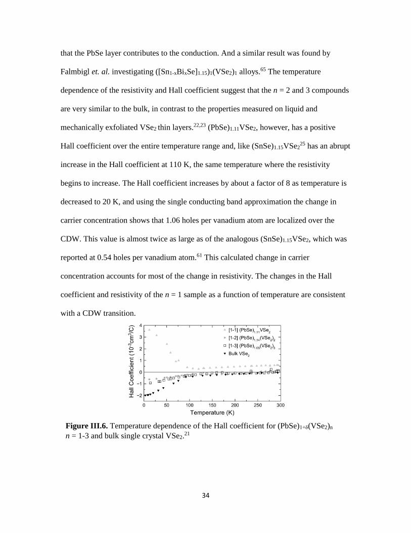
Temperature dependent Hall measurements were conducted on all samples to
provide further insight to the unusual resistivity behavior in (PbSe)1.11VSe2, and the data
obtained is plotted in Figure III.6 along with that measured for a single crystal of VSe2.21
The Hall coefficient for a single crystal of VSe2 is negative along the entire temperature
range, suggesting that electrons are the primary carrier, and has a change in slope at
approximately 110 K that was attributed to a CDW.21 The n = 3 sample also has a
negative Hall coefficient that decreases as temperature is decreased and has a change in
slope at approximately the same temperature as the bulk single crystal. The n = 2 sample
has a small positive Hall coefficient at room temperature but decreases with decreasing
temperature with a slope similar to the bulk single crystal, becoming negative at ~ 230 K.
It also has a change of slope at about 100 K. The change in sign of the Hall coefficient
suggests that at least two bands are contributing to the electrical transport, which suggests
Figure III.5. Temperature-dependent resistivity of (PbSe)1+δ(VSe2)n for n = 1-3 and
bulk VSe2.21 Resistivity normalized to room temperature resistivity for the n = 2 and 3
heterostructures and bulk VSe2 is displayed in the inset to highlight the anomalies
observed in the CDW of bulk VSe2.
34
that the PbSe layer contributes to the conduction. And a similar result was found by
Falmbigl et. al. investigating ([Sn1-xBixSe]1.15)1(VSe2)1 alloys.65 The temperature
dependence of the resistivity and Hall coefficient suggest that the n = 2 and 3 compounds
are very similar to the bulk, in contrast to the properties measured on liquid and
mechanically exfoliated VSe2 thin layers.22,23 (PbSe)1.11VSe2, however, has a positive
Hall coefficient over the entire temperature range and, like (SnSe)1.15VSe225 has an abrupt
increase in the Hall coefficient at 110 K, the same temperature where the resistivity
begins to increase. The Hall coefficient increases by about a factor of 8 as temperature is
decreased to 20 K, and using the single conducting band approximation the change in
carrier concentration shows that 1.06 holes per vanadium atom are localized over the
CDW. This value is almost twice as large as of the analogous (SnSe)1.15VSe2, which was
reported at 0.54 holes per vanadium atom.61 This calculated change in carrier
concentration accounts for most of the change in resistivity. The changes in the Hall
coefficient and resistivity of the n = 1 sample as a function of temperature are consistent
with a CDW transition.
Figure III.6. Temperature dependence of the Hall coefficient for (PbSe)1+δ(VSe2)n
n = 1-3 and bulk single crystal VSe2.21
35
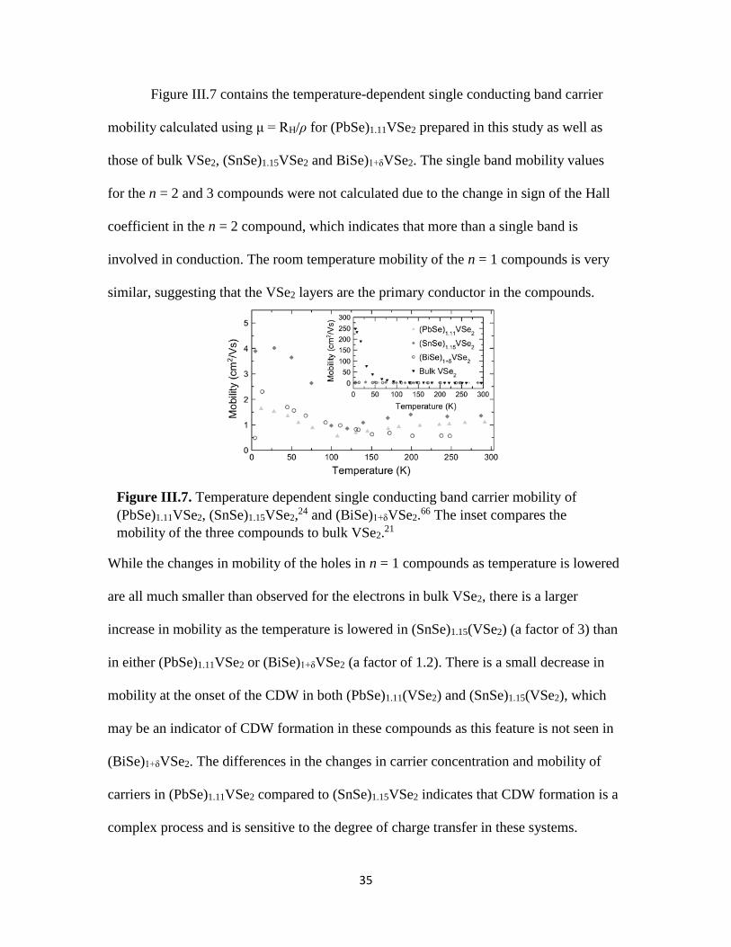
Figure III.7 contains the temperature-dependent single conducting band carrier
mobility calculated using μ = RH/ρ for (PbSe)1.11VSe2 prepared in this study as well as
those of bulk VSe2, (SnSe)1.15VSe2 and BiSe)1+δVSe2. The single band mobility values
for the n = 2 and 3 compounds were not calculated due to the change in sign of the Hall
coefficient in the n = 2 compound, which indicates that more than a single band is
involved in conduction. The room temperature mobility of the n = 1 compounds is very
similar, suggesting that the VSe2 layers are the primary conductor in the compounds.
While the changes in mobility of the holes in n = 1 compounds as temperature is lowered
are all much smaller than observed for the electrons in bulk VSe2, there is a larger
increase in mobility as the temperature is lowered in (SnSe)1.15(VSe2) (a factor of 3) than
in either (PbSe)1.11VSe2 or (BiSe)1+δVSe2 (a factor of 1.2). There is a small decrease in
mobility at the onset of the CDW in both (PbSe)1.11(VSe2) and (SnSe)1.15(VSe2), which
may be an indicator of CDW formation in these compounds as this feature is not seen in
(BiSe)1+δVSe2. The differences in the changes in carrier concentration and mobility of
carriers in (PbSe)1.11VSe2 compared to (SnSe)1.15VSe2 indicates that CDW formation is a
complex process and is sensitive to the degree of charge transfer in these systems.
Figure III.7. Temperature dependent single conducting band carrier mobility of
(PbSe)1.11VSe2, (SnSe)1.15VSe2,24 and (BiSe)1+δVSe2.
66 The inset compares the
mobility of the three compounds to bulk VSe2.21
36
The change in electrical resistivity and the sign of the Hall coefficient as the
number of VSe2 layers in the repeat unit is increased prompted us to perform DFT
calculations on both a single layer and a double layer of VSe2. The calculations were
done using the bulk 1T crystal structure of VSe2, separating either the single layer or the
double layers from one another by vacuum, and allowing the system to relax. The
resulting band structures (contained in the supplemental information) are similar to those
reported previously67,68 and indicate that 1T-VSe2 should be a metal. Unlike what was
reported for MoS2 where the Mo has trigonal prismatic coordination,69 there are only very
small differences in the band structure calculated for the single and double layer of VSe2
due to the octahedral local coordination of vanadium atoms and the 1T stacking.
Changing the position of the Fermi level in either the single or double layer of VSe2
results in changes in the density of states, but the calculations do not indicate that one or
the other have a distinct feature in the band structure that makes them more likely to have
a charge density wave transition. Figure III.8 contains a plot of the temperature
dependence of the Hall coefficients of (PbSe)1.11VSe2, (SnSe)1.15VSe2,25 and
(BiSe)1+δVSe2,66 all of which contain single VSe2 trilayers separated by a
monochalcogenide bilayer, and the temperature dependence of the Hall coefficients of
bulk VSe2.21 The compounds containing SnSe and PbSe are distinctly different from bulk
VSe2 and the compound containing BiSe. However, resistivity and Hall data reported by
Alemayehu et al. for a series of (GeSe2)m(VSe2)n heterostructures 70 indicates that CDW's
occur for a number of different n values, suggesting that a monolayer of VSe2 is not a
necessary condition for the formation of a CDW. The observed differences in transport
properties cannot be explained as only being due to a structurally isolated VSe2
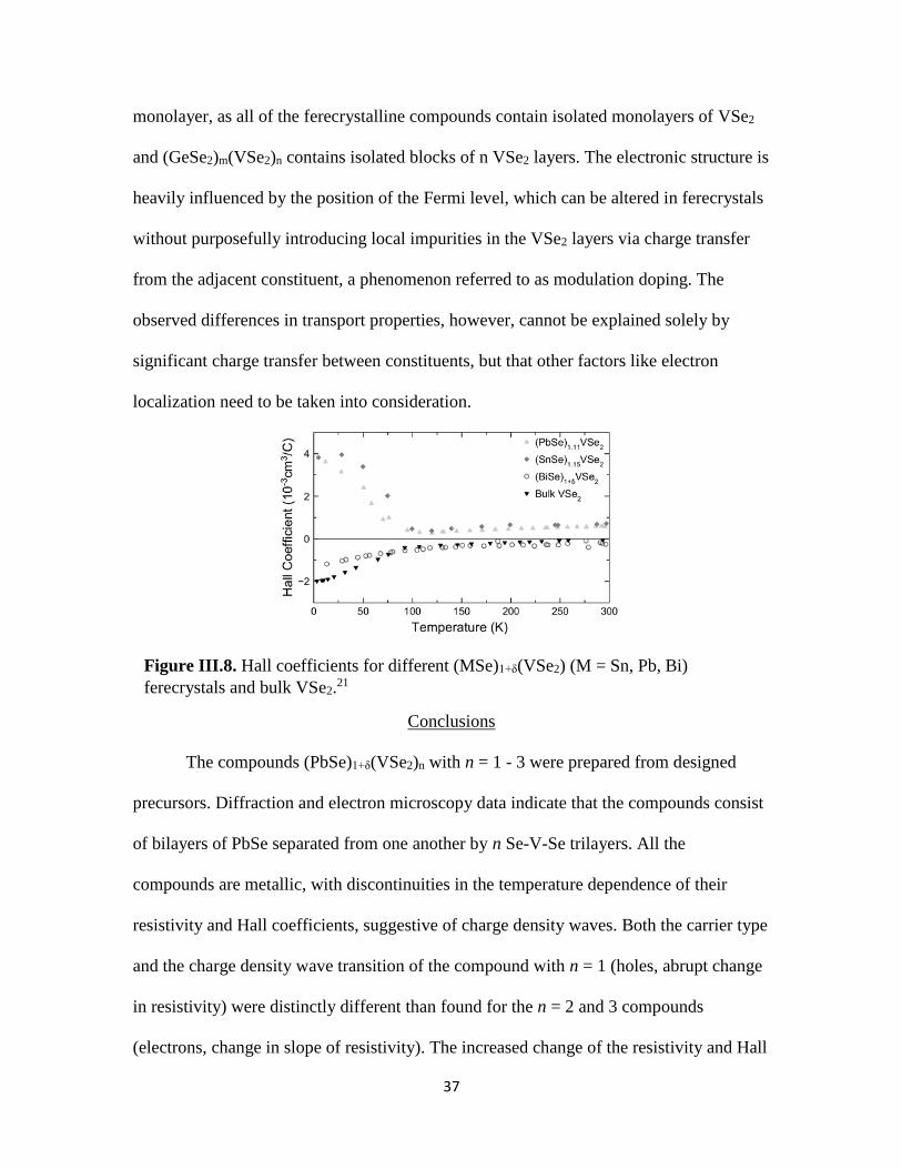
37
monolayer, as all of the ferecrystalline compounds contain isolated monolayers of VSe2
and (GeSe2)m(VSe2)n contains isolated blocks of n VSe2 layers. The electronic structure is
heavily influenced by the position of the Fermi level, which can be altered in ferecrystals
without purposefully introducing local impurities in the VSe2 layers via charge transfer
from the adjacent constituent, a phenomenon referred to as modulation doping. The
observed differences in transport properties, however, cannot be explained solely by
significant charge transfer between constituents, but that other factors like electron
localization need to be taken into consideration.
Conclusions
The compounds (PbSe)1+δ(VSe2)n with n = 1 - 3 were prepared from designed
precursors. Diffraction and electron microscopy data indicate that the compounds consist
of bilayers of PbSe separated from one another by n Se-V-Se trilayers. All the
compounds are metallic, with discontinuities in the temperature dependence of their
resistivity and Hall coefficients, suggestive of charge density waves. Both the carrier type
and the charge density wave transition of the compound with n = 1 (holes, abrupt change
in resistivity) were distinctly different than found for the n = 2 and 3 compounds
(electrons, change in slope of resistivity). The increased change of the resistivity and Hall
Figure III.8. Hall coefficients for different (MSe)1+δ(VSe2) (M = Sn, Pb, Bi)
ferecrystals and bulk VSe2.21
38
coefficient through the charge density wave transition for (PbSe)1.11VSe2 relative to
(BiSe)1+δVSe2 and bulk VSe2 demonstrates the importance of the companion layer in
controlling properties. The extent of charge transfer between constituent layers, the
magnitude of the structural misfit at the interface between constituents, the magnitude of
electron-electron correlation, and the degree of isolation of the single VSe2 layers from
one another may all contribute to the magnitude and the transition temperature of the
charge density wave.
Bridge
In order to determine if the charge density wave reported in (SnSe)1.15VSe2 was
unique to a SnSe-VSe2 heterostructure, SnSe was replaced with the isoelectronic PbSe. It
was found that (PbSe)1.11VSe2 has a higher resistivity increase as temperature is lowered
than the analogous SnSe heterostructure. It has been previously reported that in
(MSe)1+δNbSe2, M = Sn, Pb, PbSe donated more charge to NbSe2 than SnSe. This
increase in charge transfer from PbSe to VSe2 leads to an enhanced charge density wave
as evidenced by resistivity and Hall coefficient measurements. To further investigate the
effect of charge transfer on the charge density wave in VSe2, PbSe was replaced with
BiSe, which should donate up to one further electron. The work done on (BiSe)1+δVSe2 is
discussed in the following chapter.

39
CHAPTER IV
TRANSPORT PROPERTIES OF VSE2 MONOLAYERS SEPARATED BY
BILAYERS OF BISE
Authorship Statement
This work appeared in Journal of Materials Research in 2015, volume 31, issue 7,
pages 886 - 992. I am the primary author of this work. Mike Nellist assisted with sample
synthesis. Matthias Falmbigl and Mike Nellist also assisted with diffraction analysis.
Jeffery Ditto collected electron microscopy data and images. David C. Johnson is my
advisor and consulted in preparation of this manuscript.
Introduction
Research on two dimensional atomic crystals and heterostructures has grown
enormously in the last decade, sparked by the properties of monolayers being different
than properties of the bulk, to become one of the leading sub-fields in condensed matter
physics and materials science.1,2 The wavefunction of a monolayer extends beyond its
surface, decaying exponentially into the materials (or vacuum) both above and below it.
The surface (if vacuum) or interface (in a heterostructure) interactions result in structural
distortions, new phenomena, new physics and challenging chemistry. For example, MoS2
transitions from an indirect to a direct band gap semiconductor,3 the onset temperature of
superconductivity in 2H-NbSe2 decreases as the number of NbSe2 layers is decreased and
in extremely thin samples of NbSe2 superconductivity no longer persists,4 and ultrathin
layers of PbSe distort from the bulk rock salt structure, with both a puckering distortion
in and a pairing interaction between layers.5 While stability issues have limited the ability
to prepare monolayer films of many materials via a cleaving approach,6 the ability to

40
reasonably predict the structure of potential heterostructures made from 2-D atomic
constituents makes them attractive candidates for theoretical investigations that predict
properties as a function of nanoarchitecture. There are already quite a few predictions of
interesting properties reported in the literature.7,8
The interaction at the interfaces between monolayers also provides interesting
experimental opportunities to both tailor existing properties and potentially obtain
properties not found in either of the constituent materials. It has already been shown that
the properties of graphene strongly depend on the substrate on which it is grown.9 Ultra
low thermal conductivity results from rotational disorder between layers.11 Several
reports of samples containing thin layers of VSe2 differ with respect to the effect of layer
thickness on the charge density wave that occurs at 100K in the bulk single crystals.12 If
prepared via liquid exfoliation, the CDW increases to 135 K13 as thickness is reduced to
4-8 trilayers of VSe2. In VSe2 micromechanically exfoliated nanoflakes, the CDW onset
temperature was reported to decrease to 81 K at 11.6 nm, the lowest thickness
measured.14 In turbostratically disordered single layers of VSe2 separated by layers of
SnSe prepared using a self-assembly approach, a CDW has been reported that has an
opposite carrier type (holes) than the bulk (electrons),15 which does not occur when the
VSe2 thickness is increased beyond a monolayer.16 An understanding of how to control
properties based on the interaction between layers is developing as more heterostructures
and their properties are reported.
The change in carrier type and CDW reported for SnSe-VSe2 heterostructures
relative to bulk VSe2 prompted us to prepare a new heterostructure consisting of
alternating layers of BiSe and VSe2. BiSe was chosen as a companion layer due to the

41
prior literature on BiSe-dichalcogenide misfit compounds, which showed that the
transport properties of (BiSe)1.10NbSe2 and (BiSe)1.09TaSe2 are very similar to those of
the analogous Sn compound.17 Localization of the additional valence electron of the Bi
within the BiX subsystem has been proposed as a reason for the similar transport
properties.18 The charge is localized in Bi-Bi bonds at anti-phase boundaries, which are
thought to systematically occur due to the mutual accommodation of the lattice mismatch
to form a commensurate structure.17,19 We find that the VSe2 layer(s) in a superlattice
containing single layers of BiSe and VSe2 is structurally similar to what was previously
reported for [(SnSe)1.15]1(VSe2)1. The in-plane diffraction pattern and layer positions
from Rietveld refinement of the specular diffraction pattern are consistent with BiSe
having a rocksalt type structure. HAADF-STEM images, however, reveal extensive
turbostratic disorder and the presence of anti-phase boundaries seen previously in BiSe
containing misfit layer compounds. This suggests that the presence of anti-phase
boundaries are not dependent on forming an ordered long range distortion of both
constituent structures to form a coherent crystal. Despite the similarity of the structure of
the VSe2 single layers, no CDW is observed in the BiSe-VSe2 heterostructure. The BiSe-
VSe2 heterostructure has a negative Hall coefficient, indicating n-type carriers
predominate, which is similar to bulk VSe2.12 Since [(SnSe)1.15]m(VSe2)1 heterostructures
have positive Hall coefficients, indicating that holes are the predominant carrier, the
change of carrier type in the BiS -VSe2 heterostructure prevents formation of the CDW.
Experimental
The compound [(BiSe)1+δ]1(VSe2)1 was synthesized using the modulated
elemental reactants (MER) technique in a custom built high-vacuum physical vapor
42
deposition chamber.20 Elemental sources of Bi (99.995%) and V (99.8%), obtained from
Alfa Aesar, were evaporated at a rate of 0.4 Å/s using Thermionics 3kW electron-beam
guns onto (100) oriented Si wafers. Se (99.999%) was deposited at a rate of 0.5 Å/s
utilizing a Knudsen effusion cell. Rates were monitored using quartz crystal monitors
positioned 25 cm above the elemental sources. A custom-made LabView program
controlled the rotation of the carousel with the mounted Si wafers over the desired
elemental sources to obtain the desired deposition sequence. Pneumatically powered
shutters allow a precise control of atomic composition based on the opening time of the
shutter. The Se-Bi-Se-V layering sequence was repeated until a total thickness of 45-55
nm of the modulated precursor was obtained. To determine optimal annealing conditions
for self-assembly the precursors were annealed between 200 °C - 550 °C for 20 minutes.
X-ray diffraction, discussed below, was used to determine optimal temperature.
To form the ferecrystalline products, the precursors were annealed for 20 minutes
in a N2 glove box with oxygen content below 0.6 ppm and the resulting products
characterized using X-ray scattering. X-ray diffraction (XRD) were performed to
determine repeat unit thickness of the film. XRD measurements were performed on a
Bruker D8 Discover diffractometer equipped with Cu Kα radiation, Göbel mirrors, and
Bragg-Brentano optics geometry. Locked coupled θ-2θ scans were taken from 0-9° 2θ for
XRR and 5-65° 2θ for XRD. Samples were prepared for STEM on a FEI Helios 600
dual-beam using methods developed by Schaffer et al.21 High-angle Annular Dark-field
Scanning Transmission Electron Microscopy (HAADF-STEM) images were taken on a
FEI Titan 80-300 FEG-TEM at the Center for Advanced Materials Characterization in
Oregon (CAMCOR).
43
The Van der Pauw technique22 was used to determine temperature-dependent
resistivity and Hall coefficient of the sample in a temperature range of 20-295 K.
Samples for electrical resistivity and Hall measurements were deposited on fused Quartz
crystal slides. Using a shadow mask, a 1 cm x 1 cm cross geometry was deposited and
indium contacts were placed on the points of the cross. By sourcing a current between
two adjacent contacts and measuring the voltage on the remaining two contacts, an
average sheet resistance at a fixed temperature can be found.
Resistivity, ρ, can be found by converting the average sheet resistance, R, into resistivity
by using thickness (d) of the sample and the cross pattern symmetry (f). The Hall
coefficient was also determined using the Van der Pauw technique by sourcing a current
of 100 mA between two opposing contacts, applying a magnetic field of 0 - 1.6 T, and
measuring the voltage induced by the magnetic field between the two remaining opposing
contacts. The Hall coefficient, RH, is the slope of the least squares fit for the measured
voltage vs. applied magnetic field curve.
Results and Discussion
The [(BiSe)1+δ]1[VSe2]1 heterostructure was synthesized using modulated
elemental reactants approach. In this approach, precursors consisting of a sequence of
elemental layers are repeatedly deposited on a nominally room temperature substrate and
then annealed to self-assemble the desired heterostructure. The sequence of elemental
layers, in this case Bi-Se-V-Se was chosen to resemble that in the targeted
heterostructure. The relative thicknesses of the elemental layers in the Bi-Se bilayer was
calibrated to yield a one to one stoichiometry and the absolute thickness was calibrated to
,ln 2
Avg Sheet
dR f
44
yield two (100) monolayers of a rock salt structured BiSe. The relative thicknesses of the
elemental layers in the V-Se bilayer was calibrated to yield a one to two stoichiometry
and the absolute thickness was calibrated to a single layer of a Se-V-Se dichalcogenide
structure. The precursors were deposited using a previously described deposition
system.20 Initial ratio of deposition thicknesses and absolute thicknesses both Bi-Se and
V-Se elemental bilayers to obtain a bilayer layer of BiSe and a structural monolayer of
VSe2 were taken from previous studies.15,23 The initial samples self-assembled in to the
desired [(BiSe)1+δ]1[VSe2]1 compound after annealing at 350°C for 20 minutes, but
broader and less intense 00l diffraction maxima than seen in previous ferecrystals11,15,25
were observed in a specular XRD scan. The lattice parameter was close, however, to the
expected one, and only 00l reflections were observed in the specular scan, suggesting the
formation of the desired compound crystallographically aligned with the c-axis
perpendicular to the substrate. We varied the initial Bi composition in the BiSe
component by 5% both above and below the ideal composition. The c-axis lattice
parameter varied from 1.178(1) nm when Bi was deficient to 1.180(1) nm when there was
excess Bi, and in both extremes the quality of XRD scans decreased, having larger line
widths and less intensity than at the ideal composition. The Bi content that gave the
largest intensity and smallest line-width was used in subsequent studies. The c-axis lattice
parameters in all of the samples are smaller than the 1.203 Å observed for
[(SnSe)1.15]1(VSe2)1.15
An annealing study was performed to determine optimal formation conditions and
the resulting specular XRD scans are shown in Figure IV.1. The as-deposited scan
contains only broad (001) and (004) reflections. After 20 minutes of annealing at 250°C,
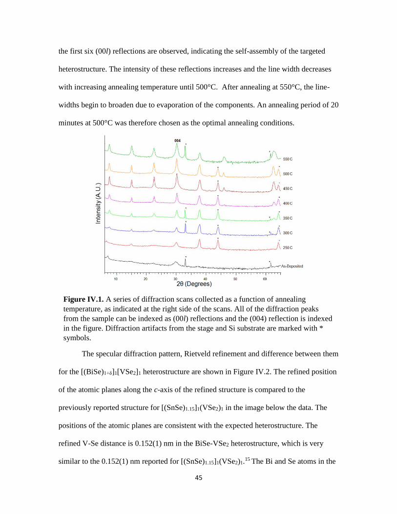
45
the first six (00l) reflections are observed, indicating the self-assembly of the targeted
heterostructure. The intensity of these reflections increases and the line width decreases
with increasing annealing temperature until 500°C. After annealing at 550°C, the line-
widths begin to broaden due to evaporation of the components. An annealing period of 20
minutes at 500°C was therefore chosen as the optimal annealing conditions.
The specular diffraction pattern, Rietveld refinement and difference between them
for the [(BiSe)1+δ]1[VSe2]1 heterostructure are shown in Figure IV.2. The refined position
of the atomic planes along the c-axis of the refined structure is compared to the
previously reported structure for [(SnSe)1.15]1(VSe2)1 in the image below the data. The
positions of the atomic planes are consistent with the expected heterostructure. The
refined V-Se distance is 0.152(1) nm in the BiSe-VSe2 heterostructure, which is very
similar to the 0.152(1) nm reported for [(SnSe)1.15]1(VSe2)1.15 The Bi and Se atoms in the
Figure IV.1. A series of diffraction scans collected as a function of annealing
temperature, as indicated at the right side of the scans. All of the diffraction peaks
from the sample can be indexed as (00l) reflections and the (004) reflection is indexed
in the figure. Diffraction artifacts from the stage and Si substrate are marked with *
symbols.
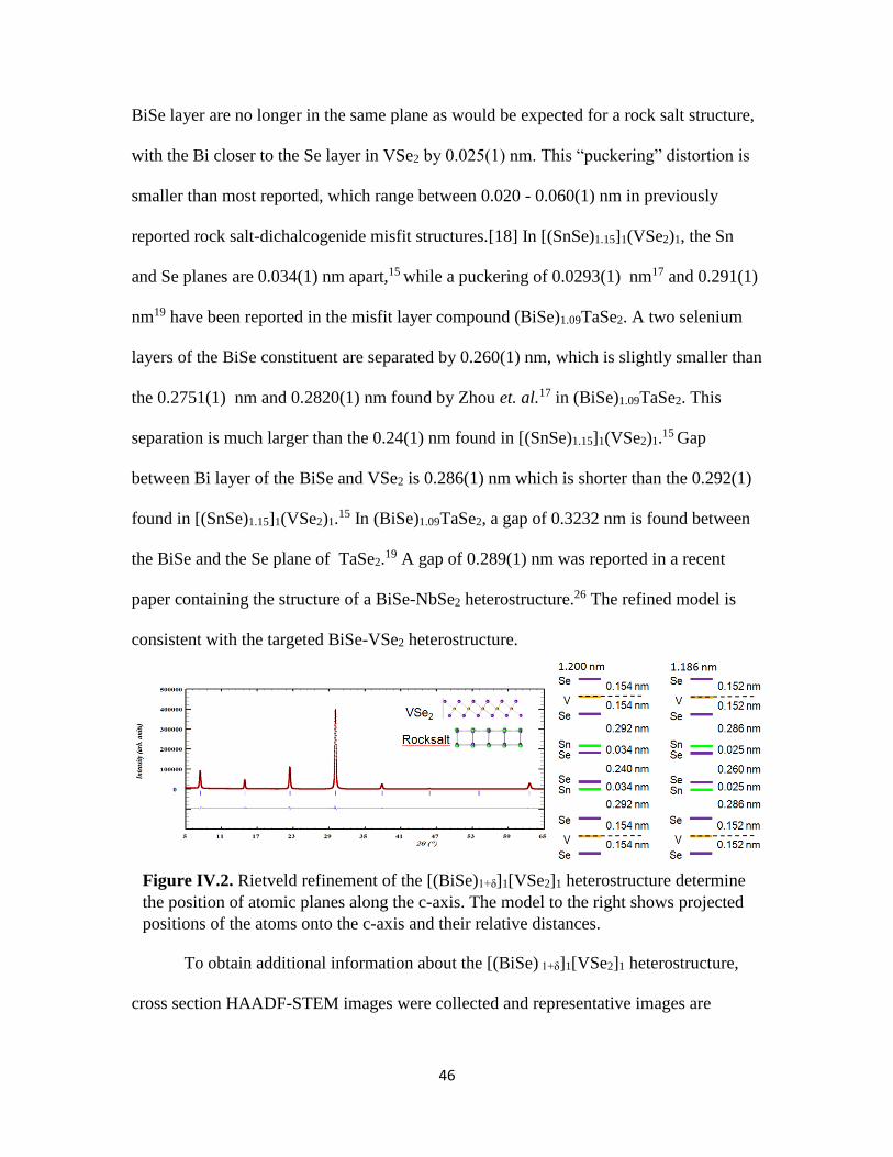
46
BiSe layer are no longer in the same plane as would be expected for a rock salt structure,
with the Bi closer to the Se layer in VSe2 by 0.025(1) nm. This “puckering” distortion is
smaller than most reported, which range between 0.020 - 0.060(1) nm in previously
reported rock salt-dichalcogenide misfit structures.[18] In [(SnSe)1.15]1(VSe2)1, the Sn
and Se planes are 0.034(1) nm apart,15 while a puckering of 0.0293(1) nm17 and 0.291(1)
nm19 have been reported in the misfit layer compound (BiSe)1.09TaSe2. A two selenium
layers of the BiSe constituent are separated by 0.260(1) nm, which is slightly smaller than
the 0.2751(1) nm and 0.2820(1) nm found by Zhou et. al.17 in (BiSe)1.09TaSe2. This
separation is much larger than the 0.24(1) nm found in [(SnSe)1.15]1(VSe2)1.15 Gap
between Bi layer of the BiSe and VSe2 is 0.286(1) nm which is shorter than the 0.292(1)
found in [(SnSe)1.15]1(VSe2)1.15 In (BiSe)1.09TaSe2, a gap of 0.3232 nm is found between
the BiSe and the Se plane of TaSe2.19 A gap of 0.289(1) nm was reported in a recent
paper containing the structure of a BiSe-NbSe2 heterostructure.26 The refined model is
consistent with the targeted BiSe-VSe2 heterostructure.
To obtain additional information about the [(BiSe) 1+δ]1[VSe2]1 heterostructure,
cross section HAADF-STEM images were collected and representative images are
Figure IV.2. Rietveld refinement of the [(BiSe)1+δ]1[VSe2]1 heterostructure determine
the position of atomic planes along the c-axis. The model to the right shows projected
positions of the atoms onto the c-axis and their relative distances.

47
contained in Figure IV.3. The structure from the top to the bottom of the film, Figure
IV.3.a, contains alternating layers of VSe2 and BiSe consistent with the targeted
heterostructure. Occasionally, there are missing layers of BiSe suggesting that the
precursor used for this STEM sample was deficient in Bi. These missing layers of BiSe,
which reduce the coherence of the structure perpendicular to the substrate, are the likely
cause of the line broadening observed in the specular diffraction patterns as composition
was varied. In higher resolution images, some of the layers are aligned along the [111]
and [100]/[010] zone axes, but the majority of the layers are not, consistent with prior
reports of extensive rotational disorder between layers for samples prepared using
modulated elemental reactants.24 Several images contained regions where some of the
BiSe layers were aligned along a zone axis, as shown in Figure IV.3.b. Clearly visible in
these layers is a periodic anti-phase boundary, similar to that previously reported for
(BiSe)1.09TaSe2.17,19
Figure IV.3. (a) Representative cross section HAADF-STEM images of the
[(BiSe)1+δ]1[VSe2]1 heterostructure. (b) Appearance of anti-phase boundaries apparent
in BiSe bilayer.
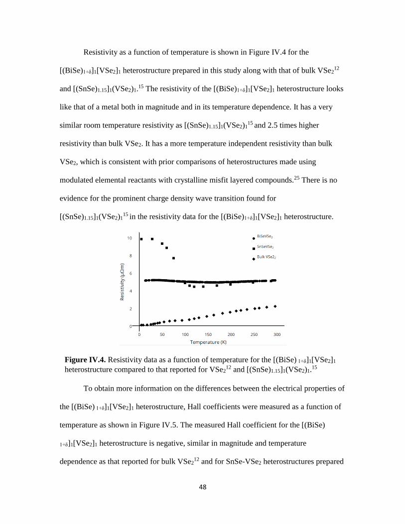
48
Resistivity as a function of temperature is shown in Figure IV.4 for the
[(BiSe)1+δ]1[VSe2]1 heterostructure prepared in this study along with that of bulk VSe212
and [(SnSe)1.15]1(VSe2)1.15 The resistivity of the [(BiSe)1+δ]1[VSe2]1 heterostructure looks
like that of a metal both in magnitude and in its temperature dependence. It has a very
similar room temperature resistivity as [(SnSe)1.15]1(VSe2)115 and 2.5 times higher
resistivity than bulk VSe2. It has a more temperature independent resistivity than bulk
VSe2, which is consistent with prior comparisons of heterostructures made using
modulated elemental reactants with crystalline misfit layered compounds.25 There is no
evidence for the prominent charge density wave transition found for
[(SnSe)1.15]1(VSe2)115 in the resistivity data for the [(BiSe)1+δ]1[VSe2]1 heterostructure.
To obtain more information on the differences between the electrical properties of
the [(BiSe) 1+δ]1[VSe2]1 heterostructure, Hall coefficients were measured as a function of
temperature as shown in Figure IV.5. The measured Hall coefficient for the [(BiSe)
1+δ]1[VSe2]1 heterostructure is negative, similar in magnitude and temperature
dependence as that reported for bulk VSe212 and for SnSe-VSe2 heterostructures prepared
Figure IV.4. Resistivity data as a function of temperature for the [(BiSe) 1+δ]1[VSe2]1
heterostructure compared to that reported for VSe212 and [(SnSe)1.15]1(VSe2)1.
15

49
with thicker VSe2 layers.16 This contrasts with the positive Hall coefficient previously
reported for [(SnSe)1.15]1(VSe2)1.15
The resistivity and Hall data reported here for the [(BiSe) 1+δ]1[VSe2]1
heterostructure is distinctly different than that reported for the analogous SnSe compound
as shown in Figures IV.4 and IV.5. [(SnSe)1.15]1(VSe2)115 is a p-type conductor and has a
significant increase in resistivity and in the Hall coefficient consistent with a charge
density wave transition. The [(BiSe)1+δ]1[VSe2]1 heterostructure is an n-type conductor
and the temperature dependence of its Hall coefficient looks very similar to that of VSe2.
The higher resistivity of the the [(BiSe)1+δ]1[VSe2]1 heterostructure likely results from a
higher concentration of defects than the equilibrium grown single crystal of VSe2.
There are several potential reasons for the difference in transport behavior
between the [(BiSe)1+δ]1[VSe2]1 and the [(SnSe)1.15]1[VSe2]1 heterostructures. One
unlikely explanation is that the V centers of the VSe2 layer in the [(BiSe)1+δ]1[VSe2]1
heterostructure adopt a trigonal prismatic coordination rather than the expected
octahedral coordination found in the [(SnSe) 1.15]1[VSe2]1 heterostructure and in bulk
Figure IV.5. Hall coefficients as a function of temperature for the [(BiSe)1+δ]1[VSe2]1
heterostructure compared to that reported for VSe212 and [(SnSe)1.15]1(VSe2)1.
15

50
VSe2. The similarity of the bond distances between the V and Se layers in both
heterostructures argues against this, although there is no direct evidence for the
coordination of the V in the VSe2 layer. A second possibility is that a difference in the
alignment of the electronic bands and the Fermi level of the SnSe and BiSe constituent
with those of the VSe2 monolayer results in a different amount of charge transfer. The
distortion of both the SnSe and BiSe bilayers in the [(MSe)1+δ]1[VSe2]1 heterostructures
relative to their bulk structures indicates the importance of the interface in determining
the structure and consequently the electronic structure. The periodic anti-phase boundary
in the BiSe bilayer has been proposed by Wiegers to localize potential conduction
electrons in Bi-Bi bonds at the anti-phase boundary in BiX containing misfit layer
compounds as a means of rationalizing the trivalent nature of Bi determined from bond
valence sum calculations with the similar electronic properties of analogous Sn
containing misfit layer compound.18 A higher conductivity of the BiSe layer relative to
that of SnSe might electronically couple with the VSe2 layers on either side of it more
strongly, changing the electronic structure. The periodic changes in the interface potential
resulting from the regular anti-phase boundaries in the BiSe layer might also prevent the
formation of the CDW. The lack of CDW in crystalline misfit layer compounds has been
proposed to result from the strong interaction between layers overwhelming the weaker
electron-phonon interactions underlying charge density wave formation.
The modular design criteria inherent to heterostructures enables one to propose
potential heterostructures to systematically test physical phenomena. For example,
preparing a repeating structure consisting of a single structural unit of VSe2-BiSe-MoSe2-
BiSe would maintain the same interfaces adjacent to the VSe2 layer, but the
51
semiconducting MoSe2 layer would reduce the through plane conductivity. If electron
localization is the driving force for the formation of anti-phase boundaries in the BiSe
bilayer, a VSe2-BiSe-VSe2-M1-xM'xSe heterostructure where M and M' had different
valences would enable the titration of the charge density. The changing charge density
might also be expected to change the frequency of the anti-phase boundary. Comparing a
VSe2-BiSe heterostructure with a VSe2-Bi2Se3 or a VSe2-PbSe heterostructure would
probe the effect of the anti-phase boundary on the CDW. Interest in heterostructures will
continue to expand as theory and experiment are able to test ideas and concepts via
systematic changes in nanostructure and nanoarchitecture.
Conclusions
The single structural layer of VSe2 in the [(BiSe)1+δ]1[VSe2]1 heterostructure has
very similar structural properties to that found in the analogous [(SnSe) 1.15]1[VSe2]1
heterostructure, but the heterostructures have very different electrical properties. The
[(BiSe)1+δ]1[VSe2]1 heterostructure is metallic with electrons as majority carriers while
the analogous [(SnSe)1.15]1[VSe2]1 heterostructure has holes as the majority carriers. The
[(SnSe)1.15]1[VSe2]1 heterostructure has large resistance and Hall coefficient change with
temperature as a consequence of a charge density wave transition, while the
[(BiSe)1+δ]1[VSe2]1 heterostructure has an almost temperature independent resistivity and
a Hall coefficient sign (negative), magnitude and temperature dependence that is very
similar to bulk VSe2. The major structural difference between the two heterostructures is
in the MSe constituent. The bilayer of SnSe adopts a rock salt structure while the BiSe
bilayer has periodic anti-phase boundaries resulting in a larger a-axis lattice parameter.
The anti-phase boundaries are thought to both localize electrons in Bi-Bi bonds and

52
potentially effectively scatter charge carriers, resulting in a low mobility. Systematic
changes in heterostructure constituents and nanoarchitecture are suggested to further
probe the effect of interfaces and charge transfer between constituents on properties.
Bridge
With the replacement of PbSe with BiSe in (MSe)1+δVSe2 the charge density
wave previously seen becomes severely dampened. However, STEM images show
antiphase boundaries within BiSe, which localize the extra electron of the bismuth to the
Bi-Bi pair. This change in interface from a rocksalt to an orthorhombic structure with
antiphase boundaries may have a significant effect on the charge density wave of the
adjacent VSe2. To further explore the effects of the interface on the charge density wave
in VSe2, BiSe was replaced with trigonal SnSe2. The structure of the (SnSe2)1+δ(VSe2)n
for n = 1-3 and electrical properties for n = 1 are discussed in the following chapter.

53
CHAPTER V
INFLUENCE OF INTERFACIAL STRUCTURE ON THE CHARGE DENSITY WAVE
IN VSE2 HETEROSTRUCTURES WITH 1T-SNSE2
Authorship Statement
This work is currently unpublished but a manuscript for publication is expected to
be prepared by myself with consultation from my advisor, David C. Johnson. I am the
primary author of this work. James Sadighian aided in collection of X-ray diffraction and
analysis. David C. Johnson is my advisor and consulted in preparation of this manuscript.
Introduction
Isolation of graphene in 2004 by Novoselov et al.1 not only lead to the awarding
of the Nobel Prize in Physics but kickstarted many efforts into the study of 2D-materials.
The resulting research has shown that the transition from a 3-dimensional bulk to a 2-
dimensional monolayer often results in changes in chemical and physical properties. A
well-known example is MoS2, which transitions from an indirect band gap in the bulk to
a direct band gap in a monolayer. The indirect band gap has been attributed to the
interaction of the d-orbitals of the S atoms with the S atoms of adjacent layers. Since this
interaction no longer exists in the isolated monolayer, the transition now becomes a direct
transition.2 A similar transition has been seen in hexagonal boron nitride (h-BN) where
the bulk band gap of 4.0 eV increases to 4.6 eV in the monolayer.3 However, much of the
work on the 2D-materials is limited to semiconducting films due to stability issues
present in thin metallic films, which readily oxidize when exposed to atmosphere.4
Heterostructures allow for isolation of materials, such as metallic monolayers, that
are not necessarily stable in atmosphere, by surrounding air-sensitive layers with several

54
oxidation resistant layers. Heterostructures also allow for systematic changes in
constituents and/or nanoarchitecture that enables a more complete understanding of
exotic properties such as superconductivity and charge density waves. Due in part to the
challenges in making finite thickness layers of metallic layered compounds, there are
considerable differences in the reported onset temperature of the charge density wave
transition in VSe2. For example, micromechanically exfoliated VSe2 layers have a
measured onset temperature of 81 K at 11.6 nm while liquid exfoliated films between 4-8
trilayers report an onset temperature of 135 K.5,6 In a series of papers of heterostructures
containing VSe2 Falmbigl et al. and Hite et al. reported that the CDW changes
significantly in character in (SnSe)1.15(VSe2)n and (PbSe)1+δ(VSe2)n when n is increased
from 1 (monolayer) to 2 (bilayer), respectively.7,8 However, only a small change in
overall resistivity and Hall coefficient was seen for n = 1 when switching from SnSe to
PbSe and is likely due to differing degrees of charge transfer from the rocksalt to the
dichalcogenide layer.
In an attempt to understand the role of the MSex layer on the CDW in VSe2
heterostructures, we prepared the compounds (SnSe2)1+δ(VSe2)n where n = 1 - 3. These
compounds contain a repeating unit of one 1T-SnSe2 and n 1T-VSe2 layers. Temperature
dependent resistivity in (SnSe2)1+δ(VSe2)1 reveals metallic like behavior above T = 120 K
with a large upturn in resistivity below 120 K similar to the CDW transition found in
(SnSe)1.15(VSe2)1 and (PbSe)1+δ(VSe2)1. A positive Hall coefficient is observed and a
concomitant upturn in Hall coefficient is also seen at 120 K further supporting the
existence of a CDW similar to that observed in (SnSe)1.15(VSe2)1 and (PbSe)1+δ(VSe2)1.
Further resistivity measurements for n = 2 and 3 are underway.
55
Experimental
(SnSe2)1+δVSe2 was synthesized in a custom built Physical Vapor Deposition
(PVD)9 using the Modulated Elemental Reactant (MER)9 technique. Precursors were
sequentially deposited on (100) oriented silicon wafers using elemental sources of Sn
(Alfa Aesar, 99.98%), V (Alfa Aesar, 99.8%), and Se (Alfa Aesar, 99.999%). The
sequence Se-Sn-Se-V was deposited in order to best match the desired stacking sequence
of the final product. Precursors were annealed in N2 atmosphere for 1 minute at 350 °C
before being placed in a close ended Pyrex tube with an ampule of solid SnSe2 and
pumped to ~10-6 torr and the tube was then sealed and further annealed for 1 hour at
250 °C.
X-ray fluorescence (XRF) was performed on a Rigaku Primus II was used to
determine the intensity in counts per second (cps) of emitted X-rays. The intensity of
these emitted X-rays are then compared to an ideal intensity determined by previously
made heterostructures containing one or more of the desired layers. For more details on
XRF see Chapter II.4. Specular X-ray diffraction (00l-XRD) was performed on a Bruker
Discover diffractometer, equipped with Cu Kα radiation (λ = 0.15418 nm), Göbel mirrors,
and Bragg-Brentano θ-2θ optics geometry, in order to determine the c-lattice parameter
of the (SnSe2)1+δVSe2 repeat unit. In-plane X-ray diffraction (hk0-XRD) was performed
on a Rigaku SmartLab, equipped with Cu Kα radiation (λ = 0.15418 nm), to determine
the in-plane lattice parameters of the SnSe2 and VSe2 layers. Annealed precursors were
prepared for High-Angle Annular Dark-Field Scanning Transmission Electron
Microscopy (HAADF-STEM) on an FEI Helios 600 dual-beam using techniques
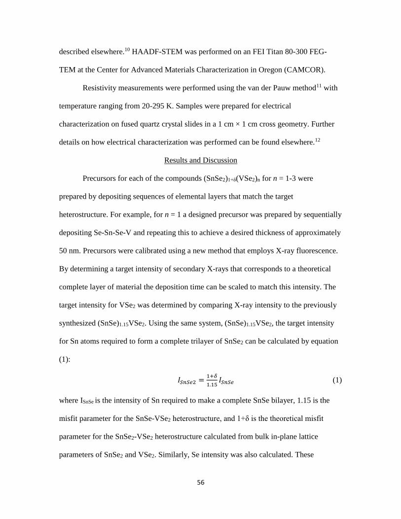
56
described elsewhere.10 HAADF-STEM was performed on an FEI Titan 80-300 FEG-
TEM at the Center for Advanced Materials Characterization in Oregon (CAMCOR).
Resistivity measurements were performed using the van der Pauw method11 with
temperature ranging from 20-295 K. Samples were prepared for electrical
characterization on fused quartz crystal slides in a 1 cm × 1 cm cross geometry. Further
details on how electrical characterization was performed can be found elsewhere.12
Results and Discussion
Precursors for each of the compounds (SnSe2)1+δ(VSe2)n for n = 1-3 were
prepared by depositing sequences of elemental layers that match the target
heterostructure. For example, for n = 1 a designed precursor was prepared by sequentially
depositing Se-Sn-Se-V and repeating this to achieve a desired thickness of approximately
50 nm. Precursors were calibrated using a new method that employs X-ray fluorescence.
By determining a target intensity of secondary X-rays that corresponds to a theoretical
complete layer of material the deposition time can be scaled to match this intensity. The
target intensity for VSe2 was determined by comparing X-ray intensity to the previously
synthesized (SnSe)1.15VSe2. Using the same system, (SnSe)1.15VSe2, the target intensity
for Sn atoms required to form a complete trilayer of SnSe2 can be calculated by equation
(1):
𝐼𝑆𝑛𝑆𝑒2 =1+𝛿
1.15𝐼𝑆𝑛𝑆𝑒 (1)
where ISnSe is the intensity of Sn required to make a complete SnSe bilayer, 1.15 is the
misfit parameter for the SnSe-VSe2 heterostructure, and 1+δ is the theoretical misfit
parameter for the SnSe2-VSe2 heterostructure calculated from bulk in-plane lattice
parameters of SnSe2 and VSe2. Similarly, Se intensity was also calculated. These

57
designed precursors were allowed to self-assemble by annealing on hotplate for 1 min at
350 °C followed by annealing in a sealed ampule at 250 °C for 1 hour.
Out-of-plane X-ray diffraction is shown in Figure V.1 and was performed on
annealed (SnSe2)1+δ(VSe2)n heterostructures for n = 1- 3. Diffraction peaks were indexed
to 00l reflections of a one trilayer Se-Sn-Se stacked on n trilayers of Se-V-Se. Repeat
units (c-lattice parameter) of 1.226(2) nm, 1.886(3) nm, and 2.495(2) nm were found for
n = 1, 2, and 3, respectively. The increase in c-lattice parameter as n is increased
corresponds to c-lattice of 0.614 nm for each VSe2 layer (bulk = 0.610 nm13). By solving
for n = 0, a c-lattice parameter for SnSe2 was found to be 0.654 nm (bulk = 0.614 nm14).
Further refinement of the structure is not possible due to the current SnSe impurity
discussed briefly below.
To further parse the structure of (SnSe2)1+δVSe2, in-plane diffraction was
performed for n = 1 – 3 revealing maxima, as seen in Figure V.2, that can be indexed to
trigonal SnSe2 and trigonal VSe2. Relative intensities for VSe2 hk0 peaks increase with
Figure V.1. Out-of-plane X-ray diffraction for (SnSe2)1+δVSe2 with maxima that are
indexed to 00l reflections.

58
the increase in the number of VSe2 layers, n, per repeat unit. The a-lattice parameters for
SnSe2 were 0.378(2) nm, 0.382(1) nm, and 0.381(2) nm for n = 1, 2, and 3, respectively,
as compared to the bulk value of 0.381 nm14. The a-lattice parameters for VSe2 were
0.340(2) nm, 0.338(1) nm, and 0.338(2) nm for n = 1, 2, and 3, respectively, as compared
to the bulk value of 0.336 nm13. The measured a-lattice parameter falls within what has
been measured previously in VSe2 containing ferecrystals, which range from 0.341(1)
nm, 0.341(3) – 0.34630(3) nm, and 0.343(6) nm were found in (SnSe)1.15VSe2,
[(SnSe)1.15]mVSe2, and (PbSe)1.11VSe2, respectively.7,8,29,30 Misfit parameters, 1+δ,
describing the ratio in area taken up by individual SnSe2 and VSe2 unit cells in the ab-
plane were determined to be 0.809(3), 0.783(2), and 0.787(3) for n = 1, 2, and 3,
respectively. Misfit parameter values of 0.99-1.2915–28 have been seen previously in
compounds containing a rocksalt and a dichalcogenide. A misfit parameter of 0.778
would be calculated using the bulk values and the slightly higher values are likely due to
Figure V.2. In-plane X-ray diffraction for (SnSe2)1+δ(VSe2)n n = 1-3. Maxima can be
indexed to hk0 peaks of 1T-SnSe2 and 1T-VSe2. A SnSe impurity peak is marked by
an asterisk.
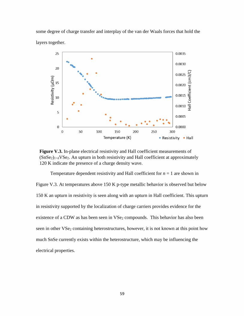
59
some degree of charge transfer and interplay of the van der Waals forces that hold the
layers together.
Temperature dependent resistivity and Hall coefficient for n = 1 are shown in
Figure V.3. At temperatures above 150 K p-type metallic behavior is observed but below
150 K an upturn in resistivity is seen along with an upturn in Hall coefficient. This upturn
in resistivity supported by the localization of charge carriers provides evidence for the
existence of a CDW as has been seen in VSe2 compounds. This behavior has also been
seen in other VSe2 containing heterostructures, however, it is not known at this point how
much SnSe currently exists within the heterostructure, which may be influencing the
electrical properties.
Figure V.3. In-plane electrical resistivity and Hall coefficient measurements of
(SnSe2)1+δVSe2. An upturn in both resistivity and Hall coefficient at approximately
120 K indicate the presence of a charge density wave.
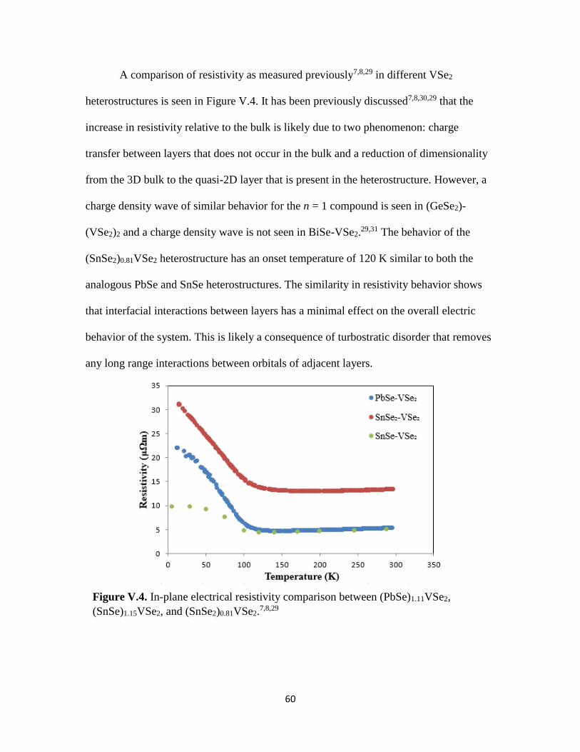
60
A comparison of resistivity as measured previously7,8,29 in different VSe2
heterostructures is seen in Figure V.4. It has been previously discussed7,8,30,29 that the
increase in resistivity relative to the bulk is likely due to two phenomenon: charge
transfer between layers that does not occur in the bulk and a reduction of dimensionality
from the 3D bulk to the quasi-2D layer that is present in the heterostructure. However, a
charge density wave of similar behavior for the n = 1 compound is seen in (GeSe2)-
(VSe2)2 and a charge density wave is not seen in BiSe-VSe2.29,31 The behavior of the
(SnSe2)0.81VSe2 heterostructure has an onset temperature of 120 K similar to both the
analogous PbSe and SnSe heterostructures. The similarity in resistivity behavior shows
that interfacial interactions between layers has a minimal effect on the overall electric
behavior of the system. This is likely a consequence of turbostratic disorder that removes
any long range interactions between orbitals of adjacent layers.
Figure V.4. In-plane electrical resistivity comparison between (PbSe)1.11VSe2,
(SnSe)1.15VSe2, and (SnSe2)0.81VSe2.7,8,29
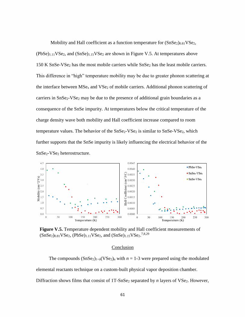
61
Mobility and Hall coefficient as a function temperature for (SnSe2)0.81VSe2,
(PbSe)1.11VSe2, and (SnSe)1.15VSe2 are shown in Figure V.5. At temperatures above
150 K SnSe-VSe2 has the most mobile carriers while SnSe2 has the least mobile carriers.
This difference in “high” temperature mobility may be due to greater phonon scattering at
the interface between MSex and VSe2 of mobile carriers. Additional phonon scattering of
carriers in SnSe2-VSe2 may be due to the presence of additional grain boundaries as a
consequence of the SnSe impurity. At temperatures below the critical temperature of the
charge density wave both mobility and Hall coefficient increase compared to room
temperature values. The behavior of the SnSe2-VSe2 is similar to SnSe-VSe2, which
further supports that the SnSe impurity is likely influencing the electrical behavior of the
SnSe2-VSe2 heterostructure.
Conclusion
The compounds (SnSe2)1+δ(VSe2)n with n = 1-3 were prepared using the modulated
elemental reactants technique on a custom-built physical vapor deposition chamber.
Diffraction shows films that consist of 1T-SnSe2 separated by n layers of VSe2. However,
Figure V.5. Temperature dependent mobility and Hall coefficient measurements of
(SnSe2)0.81VSe2, (PbSe)1.11VSe2, and (SnSe)1.15VSe2.7,8,29
62
diffraction for n = 1 shows a SnSe impurity. Resistivity and Hall coefficient
measurements were performed on (SnSe2)0.81VSe2 which revealed metallic behavior with
p-type conductance. An increase in resistivity is seen at temperatures below 120 K and
has been attributed to a charge density wave. The nature of the resistivity and Hall are
similar to analogous SnSe and PbSe compounds. This work further shows the importance
of VSe2 isolation by a semiconducting compound in enhancing the charge density wave.
Additionally, the interface appears to play a minimal role on the electric behavior and is
likely due to the rotational disorder inherent within the films that presents long range
interactions between orbitals in adjacent layers.
63
CHAPTER VI
CONCLUDING REMARKS
Authorship Statement
My advisor, David C. Johnson, was consulted in the preparation of this chapter.
Remarks
Structure and electronic properties of several VSe2 heterostructures were
synthesized using the modulated elemental reactants technique and discussed. The
modulated elemental reactants technique allows for precise synthetic control of
compounds known as ferecrystals. Precursors are composed of alternating layers of
elements that closely match the superlattice structure of the desired ferecrystal. This
unique technique produces materials that are no longer limited by diffusion and only need
to be annealed at relatively low temperatures in order to induce nucleation. This control
allows for systematic changes in the layered structure of the ferecrystal to further explore
the effects of interlayer interactions on the overall electronic properties of the ferecrystal.
This was utilized to further investigate the charge density wave that was previously
reported in the (SnSe)1.15VSe2 heterostructure.
Prior to this work Atkins and Falmbigl et al. reported a resistance anomaly at
approximately 115 K that was attributed to a charge density wave in (SnSe)1.15VSe2. With
increasing layers of VSe2 in the SnSe-VSe2 heterostructure this charge density wave was
severely dampened as a result of increased dimensionality of the VSe2. During this time
(SnSe)1.15VSe2 was the only known VSe2 heterostructure to have a charge density wave.
To determine if the charge density wave in (SnSe)1.15VSe2 was unique to this
heterostructure, SnSe was replaced with PbSe. PbSe is a layered materials with rocksalt
64
structure and is isovalent to SnSe. (PbSe)1+δ(VSe2)n for n = 1 – 3 was synthesized and
structural analysis showed that the heterostructure was composed of an alternating
structure of a distorted rocksalt PbSe and 1T-VSe2. For n = 1, a resistance anomaly at 115
K was observed similarly to the analogous (SnSe)1.15VSe2 heterostructure. Additionally,
the overall change in resistivity as temperature was lowered was higher for the PbSe
containing heterostructure as compared to the analogous SnSe heterostructure. It is
suspected that this charge density wave enhancement is due to the increased charge
transfer from the PbSe layer to the VSe2 layer. Higher values of n show resistivity
behavior that is approaching bulk resistivity and change in carrier type from p to n-type.
To further explore the effects of charge transfer on the charge density wave in VSe2,
PbSe was replaced with BiSe.
(BiSe)1+δVSe2 was prepared to determine how increased charge transfer to the
VSe2 layer influences. Electrical resistivity measurements show behavior as a function of
temperature to be similar to that of bulk VSe2. Additionally, Hall coefficient
measurements show the heterostructure to be n-type similar to bulk. HAADF-STEM
show the presence of antiphase boundaries that likely localize the additional electron the
BiSe and prevent further charge transfer. The presence of the antiphase boundaries may
also allow coupling between adjacent VSe2 layers and thereby removing the quasi two-
dimensionality of the VSe2 monolayer.
In order to understand the effects of interfacial interactions between layers and
remove the coupling between adjacent VSe2 layers, the rocksalt structure was replaced
with semiconducting 1T-SnSe2. It was found to have electrical behavior similar to that of
both SnSe and PbSe containing heterostructures. However, in-plane XRD shows peak

65
that can be indexed to a SnSe impurity that may be influencing the behavior of the
electrical resistivity. Further work is need to be performed on this system to remove the
SnSe impurity.
This work demonstrates the possibility of isolating a metallic monolayer within a
a heterostructure and using adjacent layers to control the electrical behavior of the entire
heterostructure. The electrical behavior is largely determined by the composition of the
metallic layer and the number of layers found therein. However, future studies will be
needed to further understand the role of dimensionality in the electrical behavior of
layered metallic systems.
66
APPENDIX
SUPPORTING INFORMATION FOR CHARGE DENSITY WAVE
TRANSITION IN (PBSE)1+Δ(VSE2)N COMPOUNDS WITH N = 1, 2, AND 3
Band Structure Calculations on 1T-VSe2 Monolayers and Bilayers
Density functional theory (DFT) calculations were performed using the Vienna ab
initio simulation package (vasp).1–4 The interactions of the electrons with the ionic core
were described using the projector augmented wave (PAW) method.5,6 To describe
exchange and correlation, the functionals of Perdew-Burke-Ernzerhof (PBE) were used.7
A cutoff energy of 500 eV was used to expand the wave functions. To reduce interactions
between periodic images, vacuum of 25 Å was added between VSe2 monolayers and
bilayers. For structural relaxations, a Γ-centered 18×18×1 k-point mesh was used. Since
interactions between VSe2 layers are of van-der-Waals type, dispersion corrections were
added using Dion’s method in the vdW-DF corrected optPBE functionals.8–11
The in-plane lattice parameters are 0.337 nm for the monolayer and 0.338 nm for
the bilayer, which is slightly smaller than in the ferecrystals, but consistent with prior
theoretical results.12,13 The distance between the V and Se layers in the monolayer is
0.158 nm, which is consistent with experimental results. For the bilayer, the distances
between the V and Se layers are slightly asymmetric: 0.158 nm for the Se layers adjacent
to the vacuum, and 0.157 nm for the remaining layers. The distance between the two VSe2
trilayers is 0.316 nm. Both the monolayer and the bilayer are ferromagnetic with a
magnetization of 0.64 and 0.66 μB/f.u., respectively.
The band structures of a pristine VSe2 monolayer and bilayer are shown in Figure
A.1. The majority spin bands for the monolayer are metallic with a hole-like Fermi surface
near the K point, whereas the minority spin bands are semi-metallic with a valence band
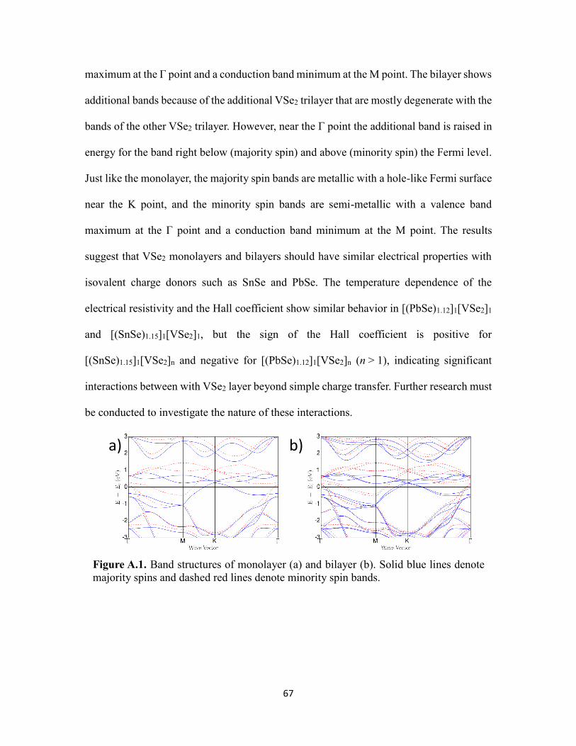
67
maximum at the Γ point and a conduction band minimum at the M point. The bilayer shows
additional bands because of the additional VSe2 trilayer that are mostly degenerate with the
bands of the other VSe2 trilayer. However, near the Γ point the additional band is raised in
energy for the band right below (majority spin) and above (minority spin) the Fermi level.
Just like the monolayer, the majority spin bands are metallic with a hole-like Fermi surface
near the K point, and the minority spin bands are semi-metallic with a valence band
maximum at the Γ point and a conduction band minimum at the M point. The results
suggest that VSe2 monolayers and bilayers should have similar electrical properties with
isovalent charge donors such as SnSe and PbSe. The temperature dependence of the
electrical resistivity and the Hall coefficient show similar behavior in [(PbSe)1.12]1[VSe2]1
and [(SnSe)1.15]1[VSe2]1, but the sign of the Hall coefficient is positive for
[(SnSe)1.15]1[VSe2]n and negative for [(PbSe)1.12]1[VSe2]n (n > 1), indicating significant
interactions between with VSe2 layer beyond simple charge transfer. Further research must
be conducted to investigate the nature of these interactions.
a) b)
Figure A.1. Band structures of monolayer (a) and bilayer (b). Solid blue lines denote
majority spins and dashed red lines denote minority spin bands.

68
Rietveld Refinement Details
The X-ray pattern (00l-reflections) for (PbSe)1.11VSe2 was refined via the Rietveld
method employing the FullProf program.14 Refinement details are found in Table A.1.
Table A.1. Rietveld refinement results from room temperature XRD data. Space group:
P-3m1 (VSe2), Fm-3m (PbSe).
69
REFERENCES CITED
Chapter I
(1) Geim, A. K.; Grigorieva, I. V. Van Der Waals Heterostructures. Nature 2013, 499,
419–425.
(2) Wang, H.; Yuan, H.; Sae Hong, S.; Li, Y.; Cui, Y. Physical and Chemical Tuning
of Two-Dimensional Transition Metal Dichalcogenides. Chem. Soc. Rev. 2015, 44,
2664–2680.
(3) Fujimoto, Y.; Koretsune, T.; Saito, S. Electronic Structures of Hexagonal Boron-
Nitride Monolayer: Strain-Induced Effects. J. Ceram. Soc. Japan 2014, 122, 346–
348.
(4) Gomes, L. C.; Carvalho, A. Phosphorene Analogues: Isoelectronic Two-Dimesional
Group-IV Monochalcogenides with Orthorhombic Structure. Phys. Rev. B 2015, 92,
085406.
(5) Wiegers, G. A. Misfit Layer Compounds: Structures and Physical Properties. Prog.
Solid State Chem. 1996, 24, 1–139.
(6) Yarmoshenko, Y. M.; Trofimova, V. A.; Shamin, S. N.; Solovyev, N. V; Kurmaev,
E. Z.; Ettema, A. R. H. F.; Haas, C. The X-Ray Emission Spectra and Electronic-
Structure of the Misfit Layer Compounds (BiS)1.08NbS2 and (PbS)1.14TaS2. J. Phys.
Condens. Matter 1994, 6, 3993–3998.
(7) Meerschaut, A.; Guemas, L.; Auriel, C.; Rouxel, J. Preparation, Structure
Determination and Transport Properties of a New Misfit Layer Compound: Lead
Niobium Sulfide ((PbS)1.14(NbS2)2). Eur. J. Solid State Inorg. Chem. 1990, 27, 557–
570.
(8) Wiegers, G. A.; Meetsma, A.; Haange, R. J.; van Smaalen, S.; de Boer, J. L.;
Meerschaut, A.; Rabu, P.; Rouxel, J. The Incommensurate Misfit Layer Structure of
(PbS)1.14NbS2, “PbNbS3” and (LaS)1.14NbS2, “LaNbS3”: An X-Ray Diffraction
Study. Acta Crystallogr. B 1990, 46, 324–332.
(9) Wiegers, G. A.; Meetsma, A.; de Boer, J. L.; van Smaalen, S.; Haange, R. J. X-ray
Crystal Structure Determination of the Triclinic Misfit Layer Compound
(SnS)1.20TiS2. J. Phys. Condens. Matter 1991, 3, 2603–2612.
(10) Meerschaut, A.; Auriel, C.; Rouxel, J. Structure Determination of a New Misfit
Layer Compound (PbS)1.18(TiS2)2. J. Alloys Compd. 1983, 183, 129–137.
(11) Wiegers, G. A.; Haange, R. J. Electrical Transport Properties of the Misfit Layer
Compounds (SnS)1.20TiS2 and (PbS)1.18TiS2. Eur. J. Solid State Inorg. Chem. 1991,
28, 1071–1078.
70
(12) Meerschaut, A. Misfit Layer Compounds. Curr. Opin. Solid State Mater. Sci. 1996,
1, 250–259.
(13) De Boer, J. L.; Meetsma, A.; Zeinstra, T. J.; Haange, R. J.; Wiegers, G. A. Structures
of the Misfit Layer Compounds (LaS)1.13TaS2, “LaTaS3” and (CeS)1.5TaS2,
“CeTaS3.” Acta Crystallogr. C 1991, 47, 924–930.
(14) Wulff, J.; Meetsma, A.; Haange, R. J.; de Boer, J. L.; Wiegers, G. A. Structure and
Electrical Transport Properties of the Misfit-Layer Compound (BiS)1.08TaS2. Synth.
Met. 1990, 39, 1–12.
(15) Auriel, C.; Roesky, R.; Meerschaut, A.; Rouxel, J. Structure Determination and
Electrical Properties of a New Misfit Layered Selenide [(PbSe)1.10NbSe2. Mater.
Res. Bull. 1993, 28, 247–254.
(16) Van Smaalen, S.; Meetsma, A.; Wiegers, G. A.; de Boer, J. L. Determination of the
Modulated Structure of the Inorganic Misfit Layer Compound (PbS)1.18TiS2. Acta
Crystallogr. B 1991, 47, 314–325.
(17) Wiegers, G. A.; Meetsma, A.; Haange, R. J.; de Boer, J. L. Structure and Physical
Properties of (SnS)1.18NbS2, “SnNbS3”, a Compound with Misfit Layer Structure.
Mater. Res. Bull. 1988, 23, 1551–1559.
(18) Meetsma, A.; Wiegers, G. A.; Haange, R. J.; de Boer, J. L. The Incommensurate
Misfit Layer Structure of (SnS)1.17NbS2, “SnNbS3”. I. A Study by Means of X-Ray
Diffraction. Acta Crystallogr. A 1989, 45, 285–291.
(19) Meerschaut, A.; Roesky, R.; Lafond, A.; Deudon, C.; Rouxel, J. Misfit Layered
Compounds: Polytypism, Multilayer Stages, Non-Stoichiometry and Electronic
Structure, Self-Misfit Compounds. J. Alloys Compd. 1995, 219, 157–160.
(20) Wiegers, G. A.; Haange, R. J. Electrical Transport and Magnetic Properties of the
Misfit Layer Compound (LaS)1.14NbS2. J. Phys. Condens. Matter 1990, 455.
(21) Rouxel, J.; Meerschaut, A.; Wiegers, G. a. Chalcogenide Misfit Layer Compounds.
J. Alloys Compd. 1995, 229, 144–157.
(22) Palewski, T. Rare Earth Compounds with Incommensurate Layered Structures.
Wiadomości Chem. 2003, 57, 827–854.
(23) Oosawa, Y.; Gotoh, Y.; Akimoto, J.; Tsunoda, T.; Sohma, M.; Onoda, M. Three
Types of Ternary Selenides with Layered Composite Crystal Structures Formed in
the Pb-Nb-Se System. Japanese J. Appl. Physics, Part 2 Lett. 1992, 31, L1096-
L1099.
(24) Gotoh, Y.; Goto, M.; Kawaguchi, Y.; Onoda, M. Preparation and Characterization
of a New Composite-Layered Sulfide, (PbS)1.12VS2, “PbVS3.” Mater. Res. Bull.
1990, 25, 307–314.

71
(25) Ruscher, C. H.; Haas, C.; Smaalen, S. van; Wiegers, G. A. Investigation of the
Optical Reflectivity of Misfit Layer Compounds: (MS)nTS2 (T=Ta, Nb; M=Sn, Pb,
Sm, Tb, La; 1.08<n<1.23. J. Phys. Condens. Matter 1994, 6, 2117–2128.
(26) Roesky, R.; Gressier, P.; Meerschaut, A.; Widder, K.; Geserich, H. P.; Scheiber, G.
Optical Properties and Electronic Structure of the Misfit Layer Compounds
’LnNb2X5 ' (Ln Identical to Y, La or Nd; X Identical to S or Se). J. Phys. Condens.
Matter 1994, 6, 3437–3442.
(27) Ren, Y.; Haas, C.; Wiegers, G. A. Photoelectron Spectroscopy Study of the
Electronic Structure of the Incommensurate Intergrowth Compounds ( SbS )1.15(
TiS2)n with n=1, 2. J. Phys. Condens. Matter 1995, 7, 5949–5958.
(28) Hernan, L.; Morales, J.; Pattanayak, J.; Tirado, J. L. Preparation and
Characterization of New Misfit Layer Selenides SnVSe3 and SnNb2Se5. Chem Lett
1991, 20, 1981–1984.
(29) Giang, N.; Xu, Q.; Hor, Y. S.; Williams, A. J.; Dutton, S. E.; Zandbergen, H. W.;
Cava, R. J. Superconductivity at 2.3 K in the Misfit Compound ( PbSe )1.16( TiSe2)2.
Phys. Rev. B 2010, 82, 24503.
(30) Trump, B. A.; Livi, K. J. T.; McQueen, T. M. The New Misfit Compound
(BiSe)1.15(TiSe2)2 and the Role of Deminsionality in the Cux(BiSe)1+δ(TiSe2)n Series.
J. Solid State Chem. 2014, 209, 6–12.
(31) Ohno, Y. Electron Tunneling from a Metallic TS2 Layer underneath an Ultra-Thin
MS Layer with Semiconducting Properties for Misfit-Layer Compounds. Surf. Sci.
2006, 600, 598–609.
(32) Atkins, R.; Dolgos, M.; Fiedler, A.; Grosse, C.; Fischer, S. F.; Rudin, S. P.; Johnson,
D. C. Synthesis and Systematic Trends in Structure and Electrical Properties of
[(SnSe)1.15]m(VSe2)1, m = 1, 2, 3, and 4. Chem. Mater. 2014, 26, 2862–2872.
(33) Atkins, R.; Wilson, J.; Zschack, P.; Grosse, C.; Neumann, W.; Johnson, D. C.
Synthesis of [(SnSe)1.15]m(TaSe2)n Ferecrystals: Structurally Tunable Metallic
Compounds. Chem. Mater. 2012, 24, 4594–4599.
(34) Atkins, R.; Disch, S.; Jones, Z.; Haeusler, I.; Grosse, C.; Fischer, S. F.; Neumann,
W.; Zschack, P.; Johnson, D. C. Synthesis, Structure and Electrical Properties of a
New Tin Vanadium Selenide. J. Solid State Chem. 2013, 202, 128–133.
(35) Falmbigl, M.; Fiedler, A.; Atkins, R. E.; Fischer, S. F.; Johnson, D. C. Suppressing
a Charge Density Wave by Changing Dimensionality in the Ferecrystalline
Compounds ([SnSe]1.15)1(VSe2)n. Nano Lett. 2015, 15, 943–948.
(36) Merrill, D. R.; Moore, D. B.; Ditto, J.; Sutherland, D. R.; Falmbigl, M.; Winkler,
M.; Pernau, H.-F.; Johnson, D. C. The Synthesis, Structure, and Electrical
Characterization of (SnSe)1.2TiSe2. Eur. J. Inorg. Chem. 2015, 2015, 83–91.

72
(37) Bauers, S. R.; Merrill, D. R.; Moore, D. B.; Johnson, D. C. Carrier Dilution in TiSe2
Based Intergrowth Compounds for Enhanced Thermoelectric Performance. J.
Mater. Chem. C 2015, 3, 10451–10458.
(38) Hite, O. K.; Nellist, M.; Ditto, J.; Falmbigl, M.; Johnson, D. C. Transport Properties
of VSe2 Monolayers Separated by Bilayers of BiSe. J. Mater. Res. 2016, 31, 886–
892.
(39) Alemayehu, M. B.; Mitchson, G.; Hanken, B. E.; Asta, M.; Johnson, D. C. Charge
Transfer between PbSe and NbSe2 in [(PbSe)1.14]m(NbSe2)1 Ferecrystalline
Compounds. Chem. Mater. 2014, 26, 1859–1866.
(40) Alemayehu, M. B.; Ta, K.; Falmbigl, M.; Johnson, D. C. Structure, Stability, and
Properties of the Intergrowth Compounds ([SnSe]1+δ)m(NbSe2)n . J. Am. Chem. Soc.
2015, 137, 4831–4839.
(41) Alemayehu, M. B.; Falmbigl, M.; Ta, K.; Grosse, C.; Westover, R. D.; Bauers, S.
R.; Fischer, S. F.; Johnson, D. C. Structural and Electrical Properties of
([SnSe]1+δ)m(NbSe2)1 Compounds: Single NbSe2 Layers Separated by Increasing
Thickness of SnSe. Chem. Mater. 2015, 27, 867–875.
(42) Moore, D. B.; Beekman, M.; Disch, S.; Zschack, P.; Häusler, I.; Neumann, W.;
Johnson, D. C. Synthesis, Structure, and Properties of Turbostratically Disordered
(PbSe)1.18(TiSe2)2. Chem. Mater. 2013, 25, 2404–2409.
(43) Thorne, R. E. Charge-Density-Waves Conductors. Phys. Today 1996, 63, 42.
(44) Mutka, H.; Housseau, N.; Pelissier, J.; Ayroles, R.; Roucau, C. Effects of Defects
on Charge Density Waves in Layered Dichalcogenides. Solid State Commun. 1984,
50, 161–164.
(45) Morris, R. C. Connection between Charge-Density Waves and Superconductivity in
NbSe2. Phys. Rev. Lett. 1975, 34 (18), 1164–1166.
(46) LeBlanc, a.; Nader, a. Resistivity Anisotropy and Charge Density Wave in 2H -
NbSe2 and 2H - TaSe2. Solid State Commun. 2010, 150 (29-30), 1346–1349.
(47) Yang, J.; Wang, W.; Liu, Y.; Du, H.; Ning, W.; Zheng, G.; Jin, C.; Han, Y.; Wang,
N.; Yang, Z.; Tian, M.; Zhang, Y. Thickness Dependence of the Charge-Density-
Wave Transition Temperature in VSe2. Appl. Phys. Lett. 2014, 105 (6), 063109.
(48) Samnakay, R.; Wickramaratne, D.; Pope, T. R.; Lake, R. K.; Salguero, T. T.;
Balandin, A. A. Zone-Folded Phonons and the Commensurate-Incommensurate
Charge-Density-Wave Transition in 1 T -TaSe2 Thin Films. Nano Lett. 2015, 15,
2965–2973.
(49) Goli, P.; Khan, J.; Wickramaratne, D.; Lake, R. K.; Balandin, A. A. Charge Density
Waves in Exfoliated Thin Films of Van Der Waals Materials: Evolution of Raman
Spectrum in TiSe2. Nano Lett. 2012, 12, 5941–5945.
73
(50) Xu, K.; Chen, P.; Li, X.; Wu, C.; Guo, Y.; Zhao, J.; Wu, X.; Xie, Y. Ultrathin
Nanosheets of Vanadium Diselenide: A Metallic Two-Dimensional Material with
Ferromagnetic Charge-Density-Wave Behavior. Angew. Chemie Int. Ed. 2013, 52,
10477–10481.
(51) Bayard, M.; Sienko, M. J. Anomalous Electrical and Magnetic Properties of
Vanadium Diselenide. J. Solid State Chem. 1976, 19, 325–329.
Chapter II
(1) Smeller, M. M.; Heideman, C. L.; Lin, Q.; Beekman, M.; Anderson, M. D.;
Zschack, P.; Anderson, I. M.; Johnson, D. C. Structure of Turbostratically
Disordered Misfit Layer Compounds [(PbSe)0.99]1[WSe2]1, [(PbSe)1.00]1[MoSe2]1,
and [(SnSe)1.03]1[MoSe2]<. Z. Anorg. Allg. Chem. 2012, 638, 2632–2639.
(2) Fister, L.; Li, X.-M.; McConnell, J.; Novet, T.; Johnson, D. C. Deposition System
for the Synthesis of Modulated, Ultrathin-Film Composites. J. Vac. Sci. Technol. A
1993, 11, 3014–3019.
(3) Ming, X.; Tao, Y.; Wen-xue, Y.; Ning, Y.; Cui-xiu, L.; Xhen-hong, M.; Wu-yan,
L.; Kun, T. Accurate Determination of Film Thickness by Low-Angle X-Ray
Reflectivity. Chinese Phys. Soc. 2000, 9, 833–836.
(4) Ofuji, M.; Inaba, K.; Omote, K.; Hoshi, H.; Takanishi, Y.; Ishikawa, K.; Takezoe,
H. Grazing Incidence In-Plane X-Ray Diffraction Study on Oriented Copper
Phthalocyanine Thin Films. Japan Soc. Appl. Phys. 2002, 41, 5467–5471.
(5) Fullerton, E. E.; Schuller, I. K.; Vanderstraeten, H.; Bruynseraede, Y. Structural
Refinement of Superlattices from X-Ray Diffraction. Phys. Rev. B 1992, 45, 9292–
9310.
(6) Phung, T. M.; Jensen, J. M.; Johnson, D. C.; Donovan, J. J.; Mcburnett, B. G.
Determination of the Composition of Ultra-Thin Ni-Si Films on Si: Constrained
Modeling of Electron Probe Microanalysis and X-Ray Reflectivity Data. X-Ray
Spectrom. 2008, 37, 608–614.
(7) Schaffer, M.; Schaffer, B.; Ramasse, Q. Sample Preparation for Atomic-
Resolution STEM at Low Voltages by FIB. Ultramicroscopy 2012, 114, 62–71.
(8) van der Pauw, L. J. A Method of Measuring the Resistivity and Hall Coefficient of
Lamellae of Arbitrary Shape. Philips Tech. Rev. 1958, 26, 220–224.
Chapter III
(1) Novoselov, K. S.; Geim, A. K.; Morozov, S. V; Jiang, D.; Zhang, Y.; V, D. S.;
Grigorieva, I. V; Firsov, A. A. Electrical Field Effect in Atomically Thin Carbon
Films. Science 2004, 306, 666–669.
(2) Kim, K. K.; Hsu, A.; Jia, X.; Kim, S. M.; Shi, Y.; Hofmann, M.; Nezich, D.;
Rodriguez-nieva, J. F.; Dresselhaus, M.; Palacios, T.; Kong, J. Synthesis of

74
Monolayer Hexagonal Boron Nitride on Cu Foil Using Chemical Vapor Deposition.
Nano Lett. 2011, 12, 161–166.
(3) Peng, Q.; Ji, W.; De, S. Mechanical Properties of the Hexagonal Boron Nitride
Monolayer: Ab Initio Study. Comput. Mater. Sci. 2012, 56, 11–17.
(4) Duan, X.; Wang, C.; Pan, A.; Yu, R.; Duan, X. Two-Dimensional Transition Metal
Dichalcogenides as Atomically Thin Semiconductors: Opportunities and
Challenges. Chem. Soc. Rev. 2015, 44, 8859–8876.
(5) Tan, C.; Zhang, H. Two-Dimensional Transitional Metal Dichalcogenide
Nanosheet-Based Composites. Chem. Soc. Rev. 2015, 44, 2713–2731.
(6) Wang, H.; Yuan, H.; Sae Hong, S.; Li, Y.; Cui, Y. Physical and Chemical Tuning
of Two-Dimensional Transition Metal Dichalcogenides. Chem. Soc. Rev. 2015, 44,
2664–2680.
(7) Gomes, L. C.; Carvalho, A. Phosphorene Analogues: Isoelectronic Two-Dimesional
Group-IV Monochalcogenides with Orthorhombic Structure. Phys. Rev. B 2015, 92,
085406.
(8) Fujimoto, Y.; Koretsune, T.; Saito, S. Electronic Structures of Hexagonal Boron-
Nitride Monolayer: Strain-Induced Effects. J. Ceram. Soc. Japan 2014, 122, 346–
348.
(9) Wang, M.-X.; Li, P.; Xu, J.-P.; Liu, Z.-L.; Ge, J.-F.; Wang, G.-Y.; Yang, X.; Xu, Z.-
A.; Ji, S.-H.; Gao, C. L.; Qian, D.; Luo, W.; Liu, C.; Jia, J.-F. Interface Structure of
a Topological Insulator/superconductor Heterostructure. New J. Phys. 2014, 16,
123043.
(10) Xu, J.-P.; Wang, M.-X.; Liu, Z. L.; Ge, J.-F.; Yang, X.; Liu, C.; Xu, Z. A.; Guan,
D.; Gao, C. L.; Qian, D.; Liu, Y.; Wang, Q.-H.; Zhang, F.-C.; Xue, Q.-K.; Jia, J.-F.
Experimental Detection of a Majorana Mode in the Core of a Magnetic Vortex inside
a Topological Insulator-Superconductor Bi2Te3/NbSe2 Heterostructure. Phys. Rev.
Lett. 2015, 114, 017001.
(11) Geim, A. K.; Grigorieva, I. V. Van Der Waals Heterostructures. Nature 2013, 499,
419–425.
(12) Furchi, M. M.; Pospischil, A.; Libisch, F.; Burgdörfer, J.; Mueller, T. Photovoltaic
Effect in an Electrically Tunable van Der Waals Heterojunction. Nano Lett. 2014,
14, 4785–4791.
(13) Hong, X.; Kim, J.; Shi, S.-F.; Zhang, Y.; Jin, C.; Sun, Y.; Tongay, S.; Wu, J.; Zhang,
Y.; Wang, F. Ultrafast Charge Transfer in Atomically Thin MoS2/WS2
Heterostructures. Nat. Nanotechnol. 2014, 9, 682–686.
(14) Rivera, P.; Schaibley, J. R.; Jones, A. M.; Ross, J. S.; Wu, S.; Aivazian, G.; Klement,
P.; Seyler, K.; Clark, G.; Ghimire, N. J.; Yan, J.; Mandrus, D. G.; Yao, W.; Xu, X.

75
Observation of Long-Lived Interlayer Excitons in Monolayer MoSe2-WSe2
Heterostructures. Nat. Commun. 2015, 6, 6242.
(15) Grønborg, S. S.; Ulstrup, S.; Bianchi, M.; Dendzik, M.; Sanders, C. E.; Lauritsen, J.
V; Hofmann, P.; Miwa, J. A. Synthesis of Epitaxial Single-Layer MoS2 on Au(111).
Langmuir 2015, 31, 9700–9706.
(16) El-Bana, M. S.; Wolverson, D.; Russo, S.; Balakrishnan, G.; Paul, D. M.; Bending,
S. J. Superconductivity in Two-Dimensional NbSe2 Field Effect Transistors.
Supercond. Sci. Technol. 2013, 26, 125020.
(17) Frindt, R. F. Superconductivity in Ultrathin NbSe2 Layers. Phys. Rev. Lett. 1972,
28, 299–301.
(18) Grosse, C.; Alemayehu, M. B.; Falmbigl, M.; Mogilatenko, A.; Chiatti, O.; Johnson,
D. C.; Fischer, S. F. Superconducting Ferecrystals: Turbostratically Disordered
Atomic-Scale Layered (PbSe)1.14(NbSe2)n Thin Films. Sci. Rep. 2016, 6, 33457.
(19) Gao, D.; Xue, Q.; Mao, X.; Wang, W.; Xu, Q.; Xue, D. Ferromagnetism in Ultrathin
VS2 Nanosheets. J. Mater. Chem. C 2013, 1, 5909–5916.
(20) Zhang, H.; Liu, L.-M.; Lau, W.-M. Dimension-Dependent Phase Transition and
Magnetic Properties of VS2. J. Mater. Chem. A 2013, 1, 10821–10828.
(21) Bayard, M.; Sienko, M. J. Anomalous Electrical and Magnetic Properties of
Vanadium Diselenide. J. Solid State Chem. 1976, 19, 325–329.
(22) Xu, K.; Chen, P.; Li, X.; Wu, C.; Guo, Y.; Zhao, J.; Wu, X.; Xie, Y. Ultrathin
Nanosheets of Vanadium Diselenide: A Metallic Two-Dimensional Material with
Ferromagnetic Charge-Density-Wave Behavior. Angew. Chemie Int. Ed. 2013, 52,
10477–10481.
(23) Yang, J.; Wang, W.; Liu, Y.; Du, H.; Ning, W.; Zheng, G.; Jin, C.; Han, Y.; Wang,
N.; Yang, Z.; Tian, M.; Zhang, Y. Thickness Dependence of the Charge-Density-
Wave Transition Temperature in VSe2. Appl. Phys. Lett. 2014, 105, 063109.
(24) Atkins, R.; Disch, S.; Jones, Z.; Haeusler, I.; Grosse, C.; Fischer, S. F.; Neumann,
W.; Zschack, P.; Johnson, D. C. Synthesis, Structure and Electrical Properties of a
New Tin Vanadium Selenide. J. Solid State Chem. 2013, 202, 128–133.
(25) Falmbigl, M.; Fiedler, A.; Atkins, R. E.; Fischer, S. F.; Johnson, D. C. Suppressing
a Charge Density Wave by Changing Dimensionality in the Ferecrystalline
Compounds ([SnSe]1.15)1(VSe2)n. Nano Lett. 2015, 15, 943–948.
(26) Goli, P.; Khan, J.; Wickramaratne, D.; Lake, R. K.; Balandin, A. A. Charge Density
Waves in Exfoliated Films of van der Waals Materials: Evolution of Raman
Spectrum in TiSe2. Nano Lett. 2012, 12, 5941-5945.
(27) Samnakay, R.; Wickramaratne, D.; Pope, T. R.; Lake, R. R.; Salguero, T. T.;
Balandin, A. A. Zone-Folded Phonons and the Commensurate-Incommensurate

76
Charge-Density-Wave Transition in 1T-TaSe2 Thin Films. Nano Lett. 2015, 15,
2965-2973.
(28) Atkins, R.; Dolgos, M.; Fiedler, A.; Grosse, C.; Fischer, S. F.; Rudin, S. P.; Johnson,
D. C. Synthesis and Systematic Trends in Structure and Electrical Properties of
[(SnSe)1.15]m(VSe2)1 , m = 1, 2, 3, and 4. Chem. Mater. 2014, 26, 2862–2872.
(29) Fister, L.; Li, X.-M.; McConnell, J.; Novet, T.; Johnson, D. C. Deposition System
for the Synthesis of Modulated, Ultrathin-Film Composites. J. Vac. Sci. Technol. A
1993, 11, 3014.
(30) Phung, T. M.; Jensen, J. M.; Johnson, D. C.; Donovan, J. J.; Mcburnett, B. G.
Determination of the Composition of Ultra-Thin Ni-Si Films on Si: Constrained
Modeling of Electron Probe Microanalysis and X-Ray Reflectivity Data. X-Ray
Spectrom. 2008, 37, 608–614.
(31) Schaffer, M.; Schaffer, B.; Ramasse, Q. Sample Preparation for Atomic-Resolution
STEM at Low Voltages by FIB. Ultramicroscopy 2012, 114, 62–71.
(32) Van der Pauw, L. J. A Method of Measuring the Resistivity and Hall Coefficient of
Lamellae of Arbitrary Shape. Philips Tech. Rev. 1958, 26, 220–224.
(33) Alemayehu, M. B.; Mitchson, G.; Hanken, B. E.; Asta, M.; Johnson, D. C. Charge
Transfer between PbSe and NbSe2 in [(PbSe)1.14]m(NbSe2)1 Ferecrystalline
Compounds. Chem. Mater. 2014, 26, 1859–1866.
(34) Atkins, R.; Wilson, J.; Zschack, P.; Grosse, C.; Neumann, W.; Johnson, D. C.
Synthesis of [(SnSe)1.15]m(TaSe2)n Ferecrystals: Structurally Tunable Metallic
Compounds. Chem. Mater. 2012, 24, 4594–4599.
(35) Bauers, S. R.; Merrill, D. R.; Moore, D. B.; Johnson, D. C. Carrier Dilution in TiSe2
Based Intergrowth Compounds for Enhanced Thermoelectric Performance. J.
Mater. Chem. C 2015, 3, 10451–10458.
(36) Merrill, D. R.; Moore, D. B.; Ditto, J.; Sutherland, D. R.; Falmbigl, M.; Winkler,
M.; Pernau, H.-F.; Johnson, D. C. The Synthesis, Structure, and Electrical
Characterization of (SnSe)1.2TiSe2. Eur. J. Inorg. Chem. 2015, 2015, 83–91.
(37) De Boer, J. L.; Meetsma, A.; Zeinstra, T. J.; Haange, R. J.; Wiegers, G. A. Structures
of the Misfit Layer Compounds (LaS)1.13TaS2, “LaTaS3” and (CeS)1.5TaS2,
“CeTaS3.”Acta Crystallogr. C 1991, 47, 924–930.
(38) Van Smaalen, S.; Meetsma, A.; Wiegers, G. A.; de Boer, J. L. Determination of the
Modulated Structure of the Inorganic Misfit Layer Compound (PbS)1.18TiS2. Acta
Crystallogr. B 1991, 47, 314–325.
(39) Wiegers, G. A. Misfit Layer Compounds: Structures and Physical Properties. Prog.
Solid State Chem. 1996, 24, 1–139.
77
(40) Wiegers, G. A.; Meetsma, A.; de Boer, J. L.; van Smaalen, S.; Haange, R. J. X-Ray
Crystal Structure Determination of the Triclinic Misfit Layer Compound
(SnS)1.20TiS2. J. Phys. Condens. Matter 1991, 3, 2603–2612.
(41) Wiegers, G. A.; Meetsma, A.; Haange, R. J.; van Smaalen, S.; de Boer, J. L.;
Meerschaut, A.; Rabu, P.; Rouxel, J. The Incommensurate Misfit Layer Structure of
(PbS)1.14NbS2, “PbNbS3” and (LaS)1.14NbS2, “LaNbS3”: An X-Ray Diffraction
Study. Acta Crystallogr. B 1990, 46, 324–332.
(42) Wiegers, G. A.; Meetsma, A.; van Smaalen, S.; Haange, R. J.; de Boer, J. L.
Structural Relationship between the Orthorhombic, Monoclinic and Triclinic Misfit
Layer Compounds (MS)nTS2 (M = Sn, Pb, Rare-Earth-Metals, T = Ti, V, Cr, Nb,
Ta; 1.13 < n < 1.21). Solid State Commun. 1990, 75, 689–692.
(43) Meerschaut, A.; Guemas, L.; Auriel, C.; Rouxel, J. Preparation, Structure
Determination and Transport Properties of a New Misfit Layer Compound: Lead
Niobium Sulfide ((PbS)1.14(NbS2)2). Eur. J. Solid State Inorg. Chem. 1990, 27, 557–
570.
(44) Smeller, M. M.; Heideman, C. L.; Lin, Q.; Beekman, M.; Anderson, M. D.; Zschack,
P.; Anderson, I. M.; Johnson, D. C. Structure of Turbostratically Disordered Misfit
Layer Compounds [(PbSe)0.99]1[WSe2]1, [(PbSe)1.00]1[MoSe2]1, and
[(SnSe)1.03]1[MoSe2]1. Z. Anorg. Allg. Chem. 2012, 638, 2632–2639.
(45) Moore, D. B.; Beekman, M.; Disch, S.; Zschack, P.; Häusler, I.; Neumann, W.;
Johnson, D. C. Synthesis, Structure, and Properties of Turbostratically Disordered
(PbSe)1.18(TiSe2)2. Chem. Mater. 2013, 25, 2404–2409.
(46) Ren, Y.; Baas, J.; Meetsma, A.; de Boer, J. L.; Wiegers, G. A. Vacancies and
Electron Localization in the Incommensurate Intergrowth Compound
(La0.95Se)1.21VSe2. Acta Crystallogr. B 1996, 52, 398–405.
(47) Gotoh, Y.; Onoda, M.; Akimoto, J.; Oosawa, Y. Preparation and Characterization
of New Sb-Containing Ternary Sulfides with Layered Composite Crystal Structure.
Jpn. J. Appl. Phys. 1992, 30, L1039–L1041.
(48) Gotoh, Y.; Onoda, M.; Akimoto, J.; Goto, M.; Oosawa, Y. The Layered Composite
Crystal Structure of the Ternary Sulfide, (BiS)1.07TaS2, “BiTaS3.”Jpn. J. Appl. Phys.
1992, 31, 3946–3950.
(49) Gotoh, Y.; Goto, M.; Kawaguchi, Y.; Onoda, M. Preparation and Characterization
of a New Composite-Layered Sulfide, (PbS)1.12VS2, “PbVS3.”Mater. Res. Bull.
1990, 25, 307–314.
(50) Wiegers, G. A.; Haange, R. J. Electrical Transport Properties of the Misfit Layer
Compounds (SnS)1.20TiS2 and (PbS)1.18TiS2. Eur. J. Solid State Inorg. Chem. 1991,
28, 1071–1078.

78
(51) Wiegers, G. A.; Meetsma, A.; Haange, R. J.; de Boer, J. L. Structure and Physical
Properties of (SnS)1.18NbS2, “SnNbS3”, a Compound with Misfit Layer Structure.
Mater. Res. Bull. 1988, 23, 1551–1559.
(52) Wulff, J.; Meetsma, A.; Haange, R. J.; de Boer, J. L.; Wiegers, G. A. Structure and
Electrical Transport Properties of the Misfit-Layer Compound (BiS)1.08TaS2. Synth.
Met. 1990, 39, 1–12.
(53) Yarmoshenko, Y. M.; Trofimova, V. A.; Shamin, S. N.; Solovyev, N. V; Kurmaev,
E. Z.; Ettema, A. R. H. F.; Haas, C. The X-Ray Emission Spectra and Electronic-
Structure of the Misfit Layer Compounds (BiS)1.08NbS2 and (PbS)1.14TaS2. J. Phys.
Condens. Matter 1994, 6, 3993–3998.
(54) Meerschaut, A. Misfit Layer Compounds. Curr. Opin. Solid State Mater. Sci. 1996,
1, 250–259.
(55) Meerschaut, A.; Auriel, C.; Rouxel, J. Structure Determination of a New Misfit
Layer Compound (PbS)1.18(TiS2)2. J. Alloys Compd. 1983, 183, 129–137.
(56) Meerschaut, A.; Deudon, C. Crystal Structure Studies of the 3R-Nb1.09S2 and the
2H-NbSe2 Compounds: Correlation between Nonstoichiometry and Stacking Type
(= Polytypism). Mater. Res. Bull. 2001, 36, 1721–1727.
(57) Meerschaut, A.; Roesky, R.; Lafond, A.; Deudon, C.; Rouxel, J. Misfit Layered
Compounds: Polytypism, Multilayer Stages, Non-Stoichiometry and Electronic
Structure, Self-Misfit Compounds. J. Alloys Compd. 1995, 219, 157–160.
(58) Meetsma, A.; Wiegers, G. A.; Haange, R. J.; de Boer, J. L. The Incommensurate
Misfit Layer Structure of (SnS)1.17NbS2, “SnNbS3”. I. A Study by Means of X-Ray
Diffraction. Acta Crystallogr. A 1989, 45, 285–291.
(59) Onoda, M.; Kato, K.; Gotoh, Y.; Oosawa, Y. Structure of the Incommensurate
Composite Crystal (PbS)1.12VS2. Acta Crystallogr. B 1990, 46, 487–492.
(60) Beekman, M.; Heideman, C. L.; Johnson, D. C. Ferecrystals: Non-Epitaxial Layered
Intergrowths. Semicond. Sci. Technol. 2014, 29, 064012.
(61) Falmbigl, M.; Putzky, D.; Ditto, J.; Esters, M.; Bauers, S. R.; Ronning, F.; Johnson,
D. C. Influence of Defects on the Charge Density Wave of ([SnSe]1+δ)1(VSe2)1
Ferecrystals. ACS Nano 2015, 9, 8440–8448.
(62) Barrios-Salgado, E.; Rodríguez-Guadarrama, L. A.; Garcia-Angelmo, A. R.;
Campos Álvarez, J.; Nair, M. T. S.; Nair, P. K. Large Cubic Tin Sulfide–tin Selenide
Thin Film Stacks for Energy Conversion. Thin Solid Films 2016, 615, 415–422.
(63) Wrasse, E. O.; Schmidt, T. M. Prediction of Two-Dimensional Topological
Crystalline Insulator in PbSe Monolayer. Nano Lett. 2014, 14, 5717–5720.
(64) Alemayehu, M. B.; Falmbigl, M.; Ta, K.; Grosse, C.; Westover, R. D.; Bauers, S.
R.; Fischer, S. F.; Johnson, D. C. Structural and Electrical Properties of

79
([SnSe]1+δ)m(NbSe2)1 Compounds: Single NbSe2 Layers Separated by Increasing
Thickness of SnSe. Chem. Mater. 2015, 27, 867–875.
(65) Falmbigl, M.; Hay, Z.; Ditto, J.; Mitchson, G.; Johnson, D. C. Modifying a Charge
Density Wave Transition by Modulation Doping: Ferecrystalline Compounds ([Sn1-
xBixSe]1.15)1(VSe2)1 with 0 ≤ x ≤ 0.66. J. Mater. Chem. C 2015, 3, 12308–12315.
(66) Li, F.; Tu, K.; Chen, Z. Versatile Electronic Properties of VSe2 Bulk , Few-Layers ,
Monolayer , Nanoribbons , and Nanotubes : A Computational Exploration. J. Phys.
Chem. 2014, 118, 21264–21274.
(67) Wasey, A. H. M. A.; Chakrabarty, S.; Das, G. P. Quantum Size Effects in Layered
VX2 (X = S, Se) Materials: Manifestation of Metal to Semimetal or Semiconductor
Transition. J. Appl. Phys. 2015, 117, 064313.
(68) Chhowalla, M.; Shin, H. S.; Eda, G.; Li, L.-J.; Loh, K. P.; Zhang, H. The Chemistry
of Two-Dimensional Layered Transition Metal Dichalcogenide Nanosheets. Nat.
Chem. 2013, 5, 263–275.
(69) Hite, O. K.; Nellist, M.; Ditto, J.; Falmbigl, M.; Johnson, D. C. Transport Properties
of VSe2 Monolayers Separated by Bilayers of BiSe. J. Mater. Res. 2016, 31, 886–
892.
(70) Alemayehu, M. B.; Falmbigl, M.; Ta, K.; Ditto, J.; Medlin, D. L.; Johnson, D. C.
Designed Synthesis of van Der Waals Heterostructures : The Power of Kinetic
Control. Angew. Chemie Int. Ed. 2015, 54, 15468–15472.
Chapter IV
(1) Geim, A. K. Graphene : Status and Prospects. Science. 2009, 324, 1530–1535.
(2) Wang, Q. H.; Kalantar-Zadeh, K.; Kis, A.; Coleman, J. N.; Strano, M. S. Electronics
and Optoelectronics of Two-Dimensional Transition Metal Dichalcogenides. Nat.
Nanotechnol. 2012, 7, 699–712.
(3) Wang, H.; Yuan, H.; Sae Hong, S.; Li, Y.; Cui, Y. Physical and Chemical Tuning
of Two-Dimensional Transition Metal Dichalcogenides. Chem. Soc. Rev. 2015, 44,
2664–2680.
(4) El-Bana, M. S.; Wolverson, D.; Russo, S.; Balakrishnan, G.; Paul, D. M.; Bending,
S. J. Superconductivity in Two-Dimensional NbSe2 Field Effect Transistors.
Supercond. Sci. Technol. 2013, 26, 125020.
(5) Anderson, M. D.; Heideman, C. L.; Lin, Q.; Smeller, M.; Kokenyesi, R.; Herzing,
A. a.; Anderson, I. M.; Keszler, D. a.; Zschack, P.; Johnson, D. C. Size-Dependent
Structural Distortions in One-Dimensional Nanostructures. Angew. Chemie - Int.
Ed. 2013, 52, 1982–1985.

80
(6) Geim, A. K.; Grigorieva, I. V. Van Der Waals Heterostructures. Nature 2013, 499,
419–425.
(7) Zeng, Q.; Wang, H.; Fu, W.; Gong, Y.; Zhou, W.; Ajayan, P. M.; Lou, J.; Liu, Z.
Band Engineering for Novel Two-Dimensional Atomic Layers. Small 2015, 11,
1868–1884.
(8) Qian, X.; Liu, J.; Fu, L.; Li, J. Quantum Spin Hall Effect and Topological Field
Effect Transistor in Two-Dimensional Transition Metal Dichalcogenide. Science).
2014, 346, 1344–1347.
(9) Yang, W.; Chen, G.; Shi, Z.; Liu, C.-C.; Zhang, L.; Xie, G.; Cheng, M.; Wang, D.;
Yang, R.; Shi, D.; Watanabe, K.; Taniguchi, T.; Yao, Y.; Zhang, Y.; Zhang, G.
Epitaxial Growth of Single-Domain Graphene on Hexagonal Boron Nitride. Nat.
Mater. 2013, 12, 792–797.
(10) Gong, Y.; Lei, S.; Ye, G.; Li, B.; He, Y.; Keyshar, K.; Zhang, X.; Wang, Q.; Lou,
J.; Liu, Z.; Vajtai, R.; Zhou, W.; Ajayan, P. M. Two-Step Growth of Two-
Dimensional WSe2/MoSe2 Heterostructures. Nano Lett. 2015.
(11) Heideman, C. L.; Tepfer, S.; Lin, Q.; Rostek, R.; Zschack, P.; Anderson, M. D.;
Anderson, I. M.; Johnson, D. C. Designed Synthesis , Structure , and Properties of
a Family of Ferecrystalline Compounds [(PbSe)1.00]m(MoSe2)n. J. Am. Chem. Soc.
2013, 135, 11055–11062.
(12) Bayard, M.; Sienko, M. J. Anomalous Electrical and Magnetic Properties of
Vanadium Diselenide. J. Solid State Chem. 1976, 19, 325–329.
(13) Xu, K.; Chen, P.; Li, X.; Wu, C.; Guo, Y.; Zhao, J.; Wu, X.; Xie, Y. Ultrathin
Nanosheets of Vanadium Diselenide: A Metallic Two-Dimensional Material with
Ferromagnetic Charge-Density-Wave Behavior. Angew. Chem. Int. Ed. Engl. 2013,
52, 10477–10481.
(14) Yang, J.; Wang, W.; Liu, Y.; Du, H.; Ning, W.; Zheng, G.; Jin, C.; Han, Y.; Wang,
N.; Yang, Z.; Tian, M.; Zhang, Y. Thickness Dependence of the Charge-Density-
Wave Transition Temperature in VSe2. Appl. Phys. Lett. 2014, 105, 063109.
(15) Atkins, R.; Disch, S.; Jones, Z.; Haeusler, I.; Grosse, C.; Fischer, S. F.; Neumann,
W.; Zschack, P.; Johnson, D. C. Synthesis, Structure and Electrical Properties of a
New Tin Vanadium Selenide. J. Solid State Chem. 2013, 202, 128–133.
(16) Falmbigl, M.; Fiedler, A.; Atkins, R. E.; Fischer, S. F.; Johnson, D. C. Suppressing
a Charge Density Wave by Changing Dimensionality in the Ferecrystalline
Compounds ([SnSe]1.15)1(VSe2)n. Nano Lett. 2015, 15, 943–948.
(17) Zhou, W. Y.; Meetsma, A.; de Boer, J. L.; Wiegers, G. A. Characterization and
Electrical Transport Propertis of the Misfit Layer Compounds (BiSe)1.10NbSe2 and
(BiSe)1.09TaSe2. Mater. Res. Bull. 1992, 27, 563–572.

81
(18) Wiegers, G. A. Misfit Layer Compounds: Structures and Physical Properties. Prog.
Solid State Chem. 1996, 24, 1–139.
(19) Petříček, V.; Cisarova, I.; de Boer, J. L.; Zhou, W.; Meetsma, a.; Wiegers, G. a.; van
Smaalen, S. The Modulated Structure of the Commensurate Misfit-Layer
Compound (BiSe)1.09TaSe2. Acta Cryst. 1993, B49, 258–266.
(20) Fister, L. Deposition System for the Synthesis of Modulated, Ultrathin-Film
Composites. J. Vac. Sci. Technol. A 1993, 11, 3014.
(21) Schaffer, M.; Schaffer, B.; Ramasse, Q. Sample Preparation for Atomic-Resolution
STEM at Low Voltages by FIB. Ultramicroscopy 2012, 114, 62–71.
(22) Van der Pauw, L. J. A Method of Measuring the Resistivity and Hall Coefficient of
Lamellae of Arbitrary Shape. Philips Tech. Rev. 1958, 26, 220–224.
(23) Heideman, C.; Nyugen, N.; Hanni, J.; Lin, Q.; Duncombe, S.; Johnson, D. C.;
Zschack, P. The Synthesis and Characterization of New [(BiSe)1.10]m[NbSe2]n,
[(PbSe)1.10]m[NbSe2]n, [(CeSe)1.14]m[NbSe2]n and [(PbSe)1.12]m[TaSe2]n Misfit
Layered Compounds. J. Solid State Chem. 2008, 181, 1701–1706.
(24) Grosse, C.; Atkins, R.; Kirmse, H.; Mogilatenko, A.; Neumann, W.; Johnson, D. C.
Local Structure and Defect Chemistry of [(SnSe)1.15]m(TaSe2) Ferecrystals - A New
Type of Layered Intergrowth Compound. J. Alloys Compd. 2013, 579, 507–515.
(25) Alemayehu, M. B.; Falmbigl, M.; Grosse, C.; Ta, K.; Fischer, S. F.; Johnson, D. C.
Structural and Electrical Properties of a New ([SnSe]1.16)m(NbSe2) Polytype. J.
Alloys Compd. 2015, 619, 816–868.
(26) Mitchson, G.; Falmbigl, M.; Ditto, J.; Johnson, D. C. Antiphase Boundaries in the
Turbostratically Disordered Misfit Compound (BiSe)1+δNbSe2. Inorg. Chem. 2015,
54, 10309–10315.
Chapter V
(1) Novoselov, K. S.; Geim, A. K.; Morozov, S. V; Jiang, D.; Zhang, Y.; Dubonos, S.
V; Grigorieva, I. V; Firsov, A. A. Electrical Field Effect in Atomically Thin
Carbon Films. Science. 2004, 306, 666–669.
(2) Wang, M.-X.; Li, P.; Xu, J.-P.; Liu, Z.-L.; Ge, J.-F.; Wang, G.-Y.; Yang, X.; Xu,
Z.-A.; Ji, S.-H.; Gao, C. L.; Qian, D.; Luo, W.; Liu, C.; Jia, J.-F. Interface
Structure of a Topological Insulator/superconductor Heterostructure. New J. Phys.
2014, 16, 123043.
(3) Fujimoto, Y.; Koretsune, T.; Saito, S. Electronic Structures of Hexagonal Boron-
Nitride Monolayer: Strain-Induced Effects. J. Ceram. Soc. Japan 2014, 122, 346–
348.
(4) Geim, A. K.; Grigorieva, I. V. Van Der Waals Heterostructures. Nature 2013, 499,
419–425.

82
(5) Yang, J.; Wang, W.; Liu, Y.; Du, H.; Ning, W.; Zheng, G.; Jin, C.; Han, Y.; Wang,
N.; Yang, Z.; Tian, M.; Zhang, Y. Thickness Dependence of the Charge-Density-
Wave Transition Temperature in VSe2. Appl. Phys. Lett. 2014, 105, 63109.
(6) Xu, K.; Chen, P.; Li, X.; Wu, C.; Guo, Y.; Zhao, J.; Wu, X.; Xie, Y. Ultrathin
Nanosheets of Vanadium Diselenide: A Metallic Two-Dimensional Material with
Ferromagnetic Charge-Density-Wave Behavior. Angew. Chemie Int. Ed. 2013, 52,
10477–10481.
(7) Falmbigl, M.; Fiedler, A.; Atkins, R. E.; Fischer, S. F.; Johnson, D. C. Suppressing
a Charge Density Wave by Changing Dimensionality in the Ferecrystalline
Compounds ([SnSe]1.15)1(VSe2)n. Nano Lett. 2015, 15, 943–948.
(8) Hite, O. K.; Falmbigl, M.; Alemayehu, M. B.; Esters, M.; Wood, S. R.; Johnson,
D. C. Charge Density Wave Transition in (PbSe)1+δ(VSe2)n Compounds with N =
1, 2, and 3. Chem. Mater. 2017, 29, 5646–5653.
(9) Fister, L.; Li, X.-M.; McConnell, J.; Novet, T.; Johnson, D. C. Deposition System
for the Synthesis of Modulated, Ultrathin-Film Composites. J. Vac. Sci. Technol. A
1993, 11, 3014–3019.
(10) Schaffer, M.; Schaffer, B.; Ramasse, Q. Sample Preparation for Atomic-
Resolution STEM at Low Voltages by FIB. Ultramicroscopy 2012, 114, 62–71.
(11) van der Pauw, L. J. A Method of Measuring the Resistivity and Hall Coefficient of
Lamellae of Arbitrary Shape. Philips Tech. Rev. 1958, 26, 220–224.
(12) Alemayehu, M. B.; Mitchson, G.; Hanken, B. E.; Asta, M.; Johnson, D. C. Charge
Transfer between PbSe and NbSe2 in [(PbSe)1.14]m(NbSe2)1 Ferecrystalline
Compounds. Chem. Mater. 2014, 26, 1859–1866.
(13) Bayard, M.; Sienko, M. J. Anomalous Electrical and Magnetic Properties of
Vanadium Diselenide. J. Solid State Chem. 1976, 19, 325–329.
(14) Garg, A. K. Long-Wavelength Optical Phonons in Semiconducting Mixed Layer
Crystals of the Series SnSxSe2-X (0 ≤ X ≤ 2). J. Phys. C Solid State Phys. 1986,
19, 3949–3960.
(15) Wiegers, G. A. Misfit Layer Compounds: Structures and Physical Properties.
Prog. Solid State Chem. 1996, 24, 1–139.
(16) Wiegers, G. A.; Meetsma, A.; de Boer, J. L.; van Smaalen, S.; Haange, R. J. X-
Ray Crystal Structure Determination of the Triclinic Misfit Layer Compound
(SnS)1.20TiS2. J. Phys. Condens. Matter 1991, 3, 2603–2612.
(17) Wiegers, G. A.; Meetsma, A.; Haange, R. J.; van Smaalen, S.; de Boer, J. L.;
Meerschaut, A.; Rabu, P.; Rouxel, J. The Incommensurate Misfit Layer Structure
of (PbS)1.14NbS2, “PbNbS3” and (LaS)1.14NbS2, “LaNbS3”: an X-Ray Diffraction
Study. Acta Crystallogr. B 1990, 46, 324–332.
(18) Ren, Y.; Baas, J.; Meetsma, A.; de Boer, J. L.; Wiegers, G. A. Vacancies and
Electron Localization in the Incommensurate Intergrowth Compound
83
(La0.95Se)1.21VSe2. Acta Crystallogr. B 1996, 52, 398–405.
(19) Gotoh, Y.; Onoda, M.; Akimoto, J.; Oosawa, Y. Preparation and Characterization
of New Sb-Containing Ternary Sulfides with Layered Composite Crystal
Structure. Jpn. J. Appl. Phys. 1992, 30, L1039–L1041.
(20) Wiegers, G. A.; Haange, R. J. Electrical Transport Properties of the Misfit Layer
Compounds (SnS)1.20TiS2 and (PbS)1.18TiS2. Eur. J. Solid State Inorg. Chem. 1991,
28, 1071–1078.
(21) Wiegers, G. A.; Meetsma, A.; Haange, R. J.; de Boer, J. L. Structure and Physical
Properties of (SnS)1.18NbS2, “SnNbS3”, a Compound with Misfit Layer Structure.
Mater. Res. Bull. 1988, 23, 1551–1559.
(22) Wulff, J.; Meetsma, A.; Haange, R. J.; de Boer, J. L.; Wiegers, G. A. Structure and
Electrical Transport Properties of the Misfit-Layer Compound (BiS)1.08TaS2.
Synth. Met. 1990, 39, 1–12.
(23) Yarmoshenko, Y. M.; Trofimova, V. A.; Shamin, S. N.; Solovyev, N. V; Kurmaev,
E. Z.; Ettema, A. R. H. F.; Haas, C. The X-Ray Emission Spectra and Electronic-
Structure of the Misfit Layer Compounds (BiS)1.08NbS2 and (PbS)1.14TaS2. J. Phys.
Condens. Matter 1994, 6, 3993–3998.
(24) Meerschaut, A. Misfit Layer Compounds. Curr. Opin. Solid State Mater. Sci.
1996, 1, 250–259.
(25) Meerschaut, A.; Deudon, C. Crystal Structure Studies of the 3R-Nb1.09S2 and the
2H-NbSe2 Compounds: Correlation between Nonstoichiometry and Stacking Type
(= Polytypism). Mater. Res. Bull. 2001, 36, 1721–1727.
(26) Meerschaut, A.; Roesky, R.; Lafond, A.; Deudon, C.; Rouxel, J. Misfit Layered
Compounds: Polytypism, Multilayer Stages, Non-Stoichiometry and Electronic
Structure, Self-Misfit Compounds. J. Alloys Compd. 1995, 219, 157–160.
(27) Meetsma, A.; Wiegers, G. A.; Haange, R. J.; de Boer, J. L. The Incommensurate
Misfit Layer Structure of (SnS)1.17NbS2, “SnNbS3”. I. A Study by Means of X-Ray
Diffraction. Acta Crystallogr. A 1989, 45, 285–291.
(28) Onoda, M.; Kato, K.; Gotoh, Y.; Oosawa, Y. Structure of the Incommensurate
Composite Crystal (PbS)1.12VS2. Acta Crystallogr. B 1990, 46, 487–492.
(29) Hite, O. K.; Nellist, M.; Ditto, J.; Falmbigl, M.; Johnson, D. C. Transport
Properties of VSe2 Monolayers Separated by Bilayers of BiSe. J. Mater. Res.
2016, 31, 886–892.
(30) Atkins, R.; Dolgos, M.; Fiedler, A.; Grosse, C.; Fischer, S. F.; Rudin, S. P.;
Johnson, D. C. Synthesis and Systematic Trends in Structure and Electrical
Properties of [(SnSe)1.15]m(VSe2)1, m = 1, 2, 3, and 4. Chem. Mater. 2014, 26,
2862–2872.
(31) Alemayehu, M. B.; Falmbigl, M.; Ta, K.; Ditto, J.; Medlin, D. L.; Johnson, D. C.
Designed Synthesis of van Der Waals Heterostructures : The Power of Kinetic

84
Control. Angew. Chemie Int. Ed. 2015, 54, 15468–15472.
Appendix
(1) Kresse, G.; Hafner, J. Ab Initio Molecular Dynamics for Liquid Metals. Phys. Rev.
B 1993, 47, 558–561.
(2) Kresse, G.; Hafner, J. Ab Initio Molecular-Dynamics Simulation of the Liquid-
Metal-Amorphous-Semiconductor Transition in Germanium. Phys. Rev. B 1994,
49, 14251–14269.
(3) Kresse, G.; Furthmüller, J. Efficiency of Ab Initio Total Energy Calculations for
Metals and Semiconductors Using a Plane Wave Basis Set. Comput. Mat. Sci. 1996,
6, 15–50.
(4) Kresse, G.; Furthmüller, J. Efficient Iterative Schemes for Ab Initio Total-Energy
Calculations Using a Plane-Wave Basis Set. Phys. Rev. B 1996, 54, 11169–11186.
(5) Blöchl, P. E. Projector Augmented-Wave Method. Phys. Rev. B 1994, 50, 17953–
17979.
(6) Kresse, G.; Joubert, D. From Ultrasoft Pseudopotentials to the Projector
Augmented-Wave Method. Phys. Rev. B 1999, 59, 1758–1775.
(7) Perdew, J. P.; Burke, K.; Ernzerhof, M. Generalized Gradient Approximation Made
Simple. Phys. Rev. Lett. 1996, 77, 3865–3868.
(8) Dion, M.; Rydberg, H.; Schröder, E.; Langreth, D. C.; Lundqvist, B. I. Van der
Waals Density Functional for General Geometries. Phys. Rev. Lett. 2004, 92,
246401–1.
(9) Román-Pérez, G.; Soler, J. M. Efficient Implementation of a van der Waals Density
Functional: Application to Double-Wall Carbon Nanotubes. Phys. Rev. Lett. 2009,
103, 96102.
(10) Klimeš, J.; Bowler, D. R.; Michaelides, A. Chemical Accuracy for the van der
Waals Density Functional. J. Phys. Condens. Matter 2010, 22, 22201.
(11) Klimeš, J.; Bowler, D. R.; Michaelides, A. Van der Waals Density Functionals
Applied to Solids. Phys. Rev. B - Condens. Matter Mater. Phys. 2011, 83, 195131.
(12) Li, F.; Tu, K.; Chen, Z. Versatile Electronic Properties of VSe2 Bulk , Few-Layers ,
Monolayer , Nanoribbons , and Nanotubes: A Computational Exploration. J. Phys.
Chem. 2014, 118, 21264–21274.
(13) Wasey, A. H. M. A.; Chakrabarty, S.; Das, G. P. Quantum Size Effects in Layered
VX2 (X = S, Se) Materials: Manifestation of Metal to Semimetal or Semiconductor
Transition. J. Appl. Phys. 2015, 11, 64313.
(14) Roisnel, T.; Rodriguez-Carvajal, J. WinPLOTR: A Windows tool for Powder
Diffraction Patter Analysis. Mater. Sci. Forum 2001, 118, 378-381.
Related Documents