SURFACE MODIFICATION OF F-DOPED TIN OXIDE THIN FILMS BY WET CHEMICAL ETCHING By Ackapop Katesomboon Department of Physics Faculty of Science King Mongkut's University of Technology Thonburi

By Ackapop Katesomboon Department of Physics Faculty of Science King Mongkut's University of Technology Thonburi.
Dec 26, 2015
Welcome message from author
This document is posted to help you gain knowledge. Please leave a comment to let me know what you think about it! Share it to your friends and learn new things together.
Transcript

SURFACE MODIFICATION OF F-DOPED TIN OXIDE THIN FILMS BY WET CHEMICAL ETCHING
ByAckapop Katesomboon
Department of Physics Faculty of Science King Mongkut's University of Technology
Thonburi

Outline
Conclusion2
Introduction
ExperimentResults and Discussion

Introduction
Glass
TCO
amorphous silicon
metal
LIGHT
3
Figure 1. Structure of amorphous silicon solar cell
Introduction (Cont.)
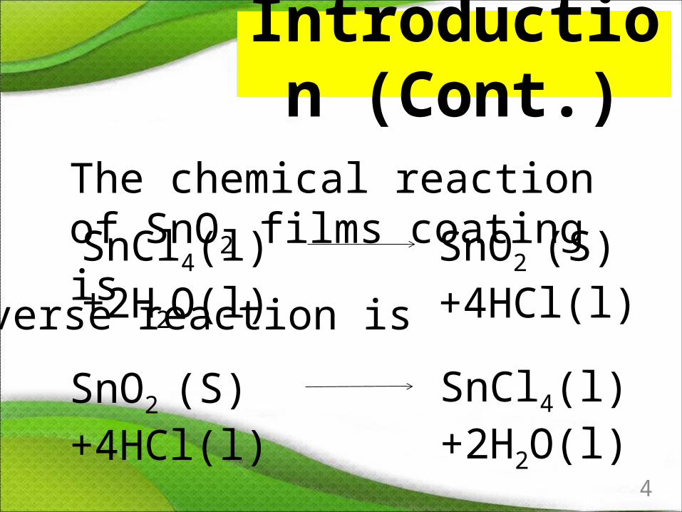
SnCl4(l)+2H2O(l)
SnO2 (S)+4HCl(l)
SnCl4(l)+2H2O(l)
SnO2 (S)+4HCl(l)
4
The chemical reaction of SnO2 films coating is
Reverse reaction is

SnO2
Glass
SnO2
SnCl4+2H2OSnO2+4HCl
UV-Vis Spectrophotometer
Atomic Force MicroscopeFour Point
Probes 5
Experiment
Percent transmissio
nrms roughness
Sheet resistance

Experiment (Cont.)
6
Effect of etching concentration / etching time
Effect of etching temperature / etching time

Table 1: Preparation conditions of etching time and HCl concentration at room temperature.Concentration
(%)
Etching time (min)
1, 3, 5 1, 5, 10, 15
7
Experiment(Cont.)
Results and Discussion
0 2 4 6 8 10 12 14 1660
62
64
66
68
70
Tra
nspa
rent
(%
)
Etching time (min)
non etching HCl 1% HCl 3% HCl 5%
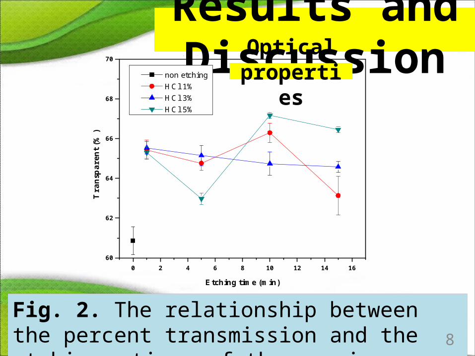
Fig. 2. The relationship between the percent transmission and the etching times of the specimens etched at different concentration.
8
Optical propertie
s
Morphological properties
Results and Discussion
9
HCl 1% 1min
Non etching
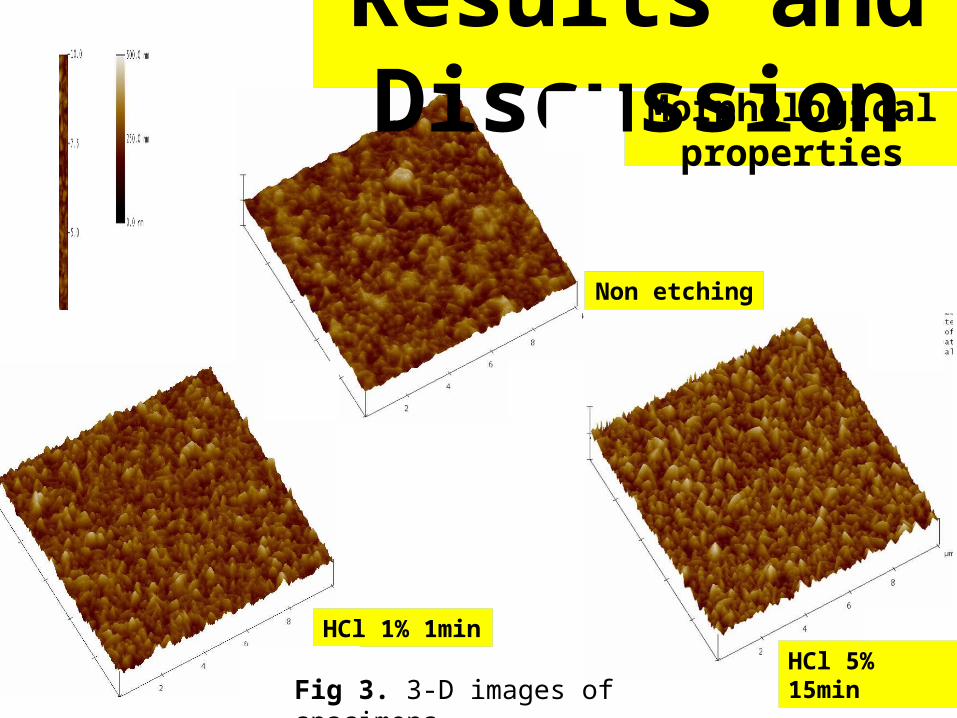
Fig 3. 3-D images of spacimensHCl 5% 15min
Etching time
(min)
Con.
(%)
Roughness rms (nm)
Roughness max (nm)
Surfacearea(µm2)
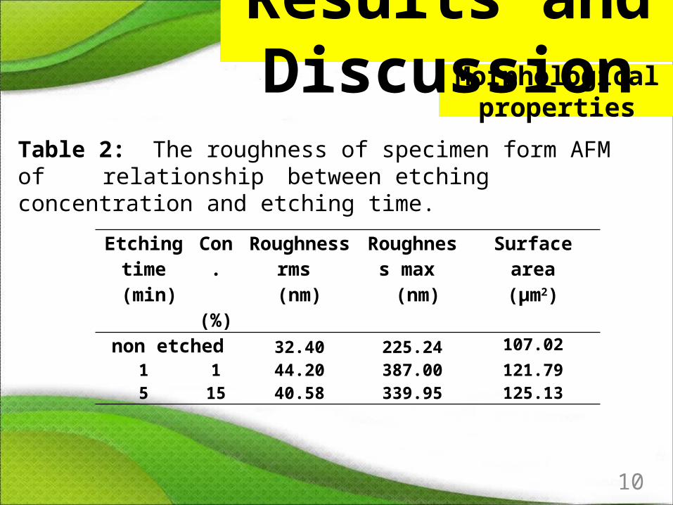
non etched 32.40 225.24 107.021 1 44.20 387.00 121.795 15 40.58 339.95 125.13
Table 2: The roughness of specimen form AFM of relationship between etching concentration and etching time.
Morphological properties
Results and Discussion
10
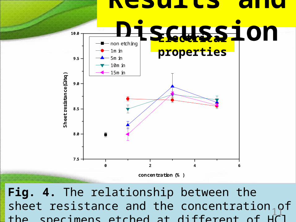
0 2 4 67.5
8.0
8.5
9.0
9.5
10.0
Sh
eet
resi
stan
ce(
/sq)
concentration (%)
non etching 1min 5min 10min 15min
Electrical properties
Fig. 4. The relationship between the sheet resistance and the concentration of the specimens etched at different of HCl etching times from 1-15 min.
11
Results and Discussion

Temperature(oC)
Etching time (min)
40, 45, 50 1, 8, 15
Table 3: Preparation condition to investigate the effect of temperature and etching time at 1% HCl concentration.
12
Experiment (Cont.)

Optical properties
34 36 38 40 42 44 46 48 5060
62
64
66
68
70
Tra
nspa
rent
(%
)
Temparature (oC)
non etching 1 min 8 min15 min
Fig. 5. The relationship between the percent transmission and the temperature of the specimens etched at different etching times.
13
Results and Discussion
14
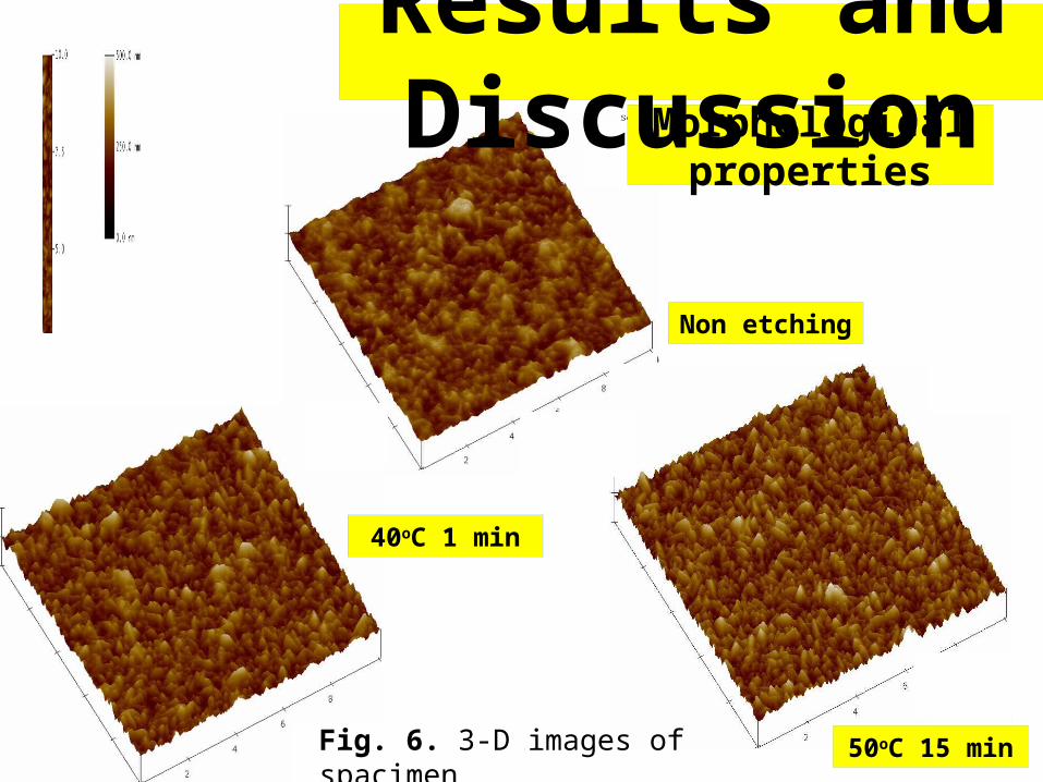
Non etching
50oC 15 min
40oC 1 min
Morphological properties
Fig. 6. 3-D images of spacimen
Results and Discussion
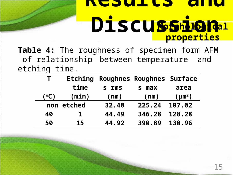
T
(oC)
Etching time(min)
Roughness rms (nm)
Roughness max (nm)
Surfacearea(µm2)
non etched 32.40 225.24 107.0240 1 44.49 346.28 128.2850 15 44.92 390.89 130.96
Table 4: The roughness of specimen form AFM of relationship between temperature and etching time.
Morphological properties
Results and Discussion
15
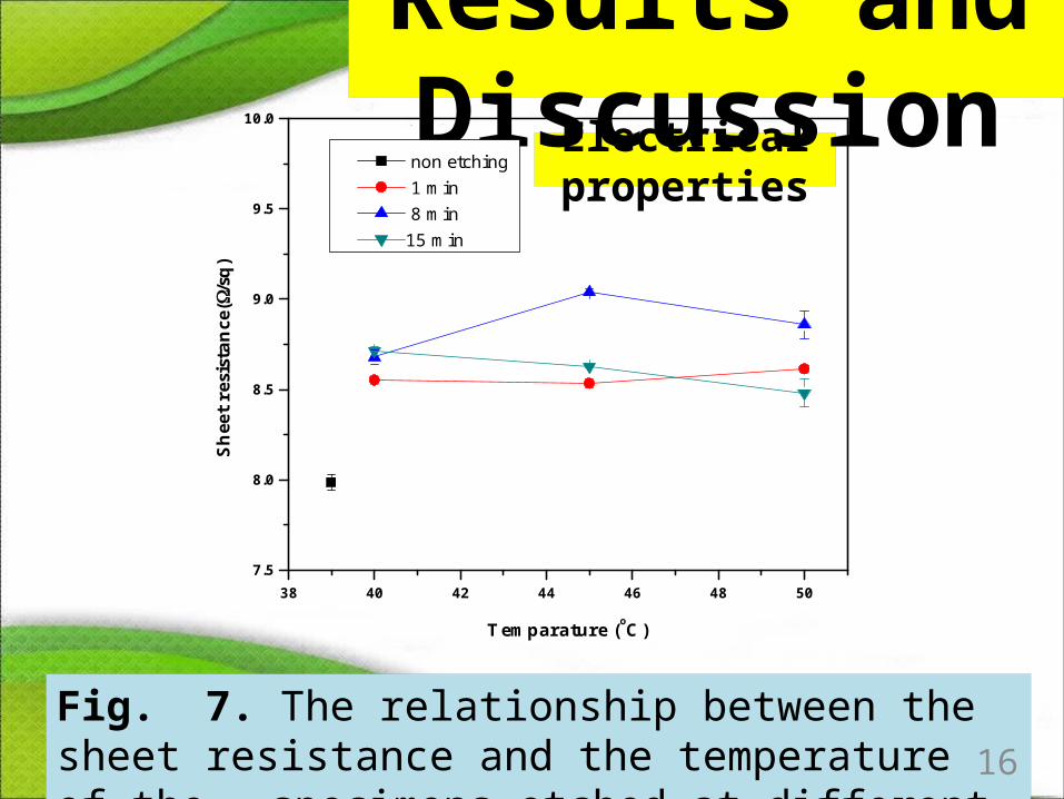
38 40 42 44 46 48 507.5
8.0
8.5
9.0
9.5
10.0
Shee
t re
sist
ance
(/s
q)
Temparature (oC)
non etching 1 min 8 min15 min
Fig. 7. The relationship between the sheet resistance and the temperature of the specimens etched at different of etching times from 1-15 min.
16
Electrical properties
Results and Discussion

Conclusion
• In the low concentration of etching concentration from 1-5%, the percent transmission, sheet resistance and morphology varied in a small region when changing etching time.• The etching temperature was
not important parameter of this experiment.
17

References
[1] N. Senoussaoui, T. Repmann, T. Brammer, H. Stiebig, H. Wangner, Rev. Energ. Ren. 3 (2000) 49-56. [2] N. Amin, T. Isaka, A. Yamada, M. Konagai, Solar Energy Materials & Solar Cells. 67 (2001) 195-201. [3] A. Krasnov, Solar Energy Materials & Solar Cells. 94 (2010) 1648-1657. [4] J. Muller, B. Rech, J. Spinger,M. Vanecek, Solar Energy, 77 (2004) 917-930.[5] A. Fuchs, H- J. Schimper, A. Klein, W. Jaegermann, Energy Procedia, 10 (2011) 149-154.[6]A. Katesomboon,S. Dumrongrattana, T. Lachit, T. Jutarosaga, W. Onreabroy, Physical Propertes of Etching F-Doped Tin Oxide Film for Photovoltaic Application, 38th Congress on Science and Technology of Thailand, Chiangmai, Thailand, (2012), p 162.
18

Acknowledgements
Supattanapong Dumrongrattana
Wandee OnreabroyTula Jutarosaga
Department of Physics Faculty of Science
King Mongkut’s University of Technology Thonburi
19
Related Documents


![King Mongkut's Institute of Technology Ladkrabang0] ComProChap0.pdfภาษาซี การเขียนโปรแกรมเบื้องต น และคําสั่ง](https://static.cupdf.com/doc/110x72/5fdfcc285e74762c1f3de6b6/king-mongkuts-institute-of-technology-0-comprochap0pdf-aaaaaa-aaaaaaaaaaaaaaaaaaaaaa.jpg)