? FNALREPORT PART II ~ ANALYSIS OF ADVANCED DATA TRANSMISSION TECHNIQUES - SEPTEMBER 1962 TO FEDERAL AVIATION AGENCY CONTRACT NO. 'FAA/BRD-80 lopeouad bV NATIONAL TECHNICAL INFORMATION SERVICE Spebog"Kl Vs- 221,51 | I GIIENERAL DYNAMICS I ELECTRONICS-ROCHESTER vro

Welcome message from author
This document is posted to help you gain knowledge. Please leave a comment to let me know what you think about it! Share it to your friends and learn new things together.
Transcript
? FNALREPORT
PART II
~ ANALYSIS OFADVANCED DATA TRANSMISSIONTECHNIQUES
-
SEPTEMBER 1962
TO FEDERAL AVIATION AGENCY
CONTRACT NO. 'FAA/BRD-80lopeouad bV
NATIONAL TECHNICALINFORMATION SERVICE
Spebog"Kl Vs- 221,51
| I
GIIENERAL DYNAMICS I ELECTRONICS-ROCHESTER vro
FINAL REPORT
PART II
ANALYSIS OF ADVANCED DATA TRANSMISSION TECHNIQUES
S GENERAL OYNAMICS I ELECTRONICS-ROCHESTER
Rochester, New Yfork
September 1962
toFEDERAL AVIATION AGENCY
Contract No. FAA/BRD-80
"This report has been prepared by General Dynamics/Ejectronics-
Rochester for the Systems Research and Development Service, FederalAviation Agency, under Contract No. FAA/BRD-80. The conte:its ofthis report reflect the views of the contractor, who is responsiblefor the facts and the accuracy of the data presented herein, and donot necessarily reflect the official views or policy of the FAA."
PREPARED BY(G. C. PorterProject Engineer
L. M. LukeSection Head
APPROVED BY: 0, , g___;LA___
T. G. flameManagerCommunications and Electronics
Advanced Development Engineering
S]i
TM3LE OF CONTENTS - PART II
Page No.
INTRODUCTION 1
Section
3.0 TEST -ACILITY
3.1 Introduction 3-1
3.2 Function 3-1
3-3 Signal 3-1
3.4 Layout 3-2
3 5 Diagrams 3-3
3.6 Power Requirements 3-3
3.7 Facility 3-3
3.7.1 Clock Pulse Generator 3-3
3.7.2 Transmit Character Pu'.[se Generator 3-5
3.7.3 Receive Character Pulse Generator 3-6
[- 3.7.4 Pattern Generator 3-6
3.7.5 Receiving Register and Comparators 3-7
1 3.7.6 Mechanical Counters 3-8
3.7.7 Divide-by-10 Decimal Decoder and Meter Indicator 3-9
3.8 Facility Logic and Counter Functions 3-10
3.9 Facility Operating Procedure 3-10
3.10 Keyer and Converter 3-il
3.10.1 Keyer 3-121.
3.10.2 Band Pass Filters 3-13
1. 3.10.3 900 Phase Shift Integrator 3-13
3.10.4 Limiter Amplifiers 3-14
!!..
I °
V secTti• (IT? CONTENTS PART II (Cont :d.)
SSection Page No.
3.10.5 Driver Amplifiers 3-11.
3.10.6 Power Amplifiers 3-14
3.10,7 Phase Detector 3-15
3.10.8 Low Pass Filter and Emitter F',1lower Driver 3-15
3.10.9 Decision Circuit 3-16
3.10.10 Mixer Amplifier 3-16
3.11 Noise Feedback Control 3-16
3.12 Keyer and Converter Operating Proc dure 3-18
4.0 CONVERTER- DF,,IGN
4.1 Introduct Ion 4-1
4.2 Converter Operation 4-1
4.3 Converter Zrcuit Design 4-2
4.3.1 Mixer Ar olifier 4-2
4.3.2 Bandress Filters 4 34.3.3 Limiters 43
4.3.4 Integzretor 4-4
4.3.5 Driver azd Power Amplifiers 4-5
4.3.6 Phase Dtc.c 4-5
4.3.7 Low Pass riiver 4-6
k.j.• Deeision CLrcuit 4-7
4.4 Noise Source 4-7
4.5 Initial Converter Set Up 4-9
4.5 Converter Waveforms 4-10
4.7 Conclusions 4-12
iii
3

TABLE OF CONTk1TS - PART II (Cont'd.)
-ction
9.0 SCHEMATICS and BLOCK DIAGRAMS
S-1 Mechanical Conter Power Supply
S-2 Inverter, Two Input NOR Gate, Emitter Follower
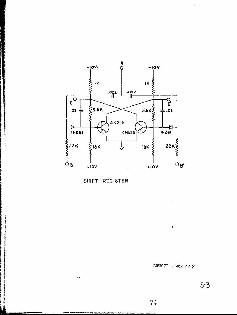
S-3 Shift Register
S-4 Divide-by-10, NOR gate, AND Transistor Gate
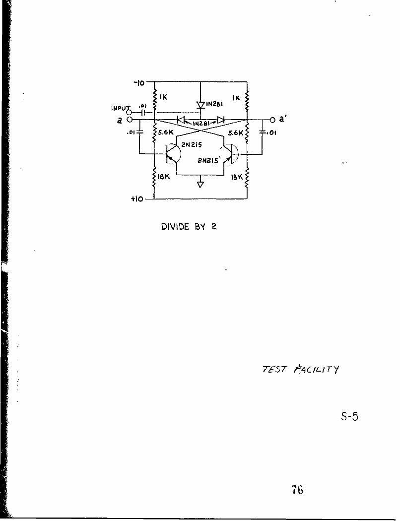
S-5 Divide -by-2
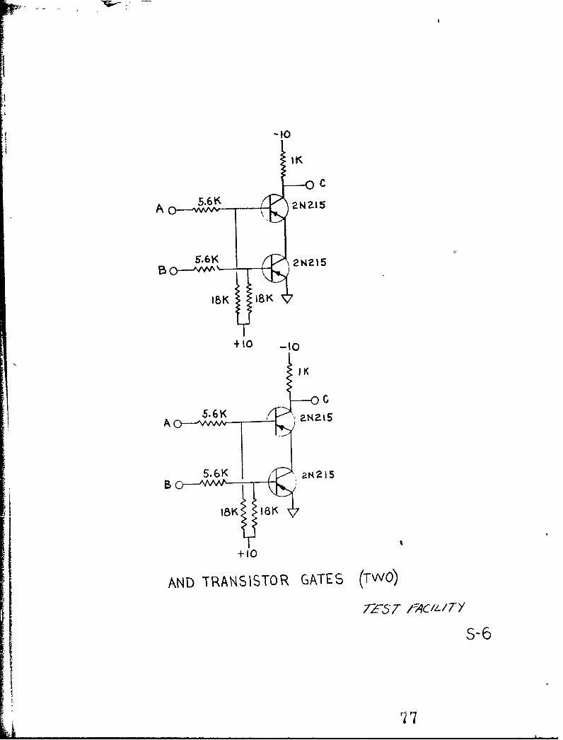
S-6 AND Transistor Gates (Two)
S-7 ]MV and Driver
S-8 Divide-by-8, NOR Gate
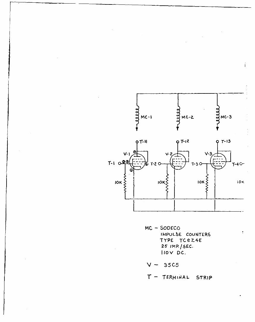
S-9 Mechanical Counter Unit
S-10 Comparator 1 Bit
S-11 Comparator 5 Bit
S-12 4kc Oscillator; EF 15; INV. 1, 36, 38, 39; Diff. 1
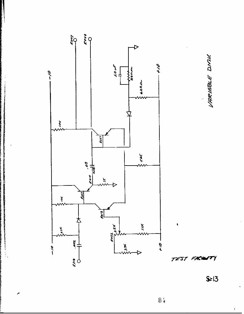
8-13 Variable DMV
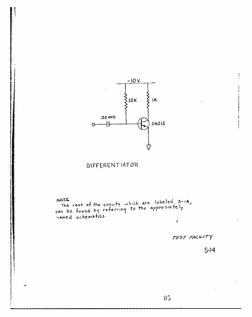
S-14 Differentiator
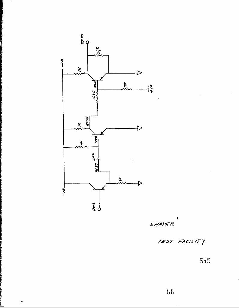
S-15 Shaper
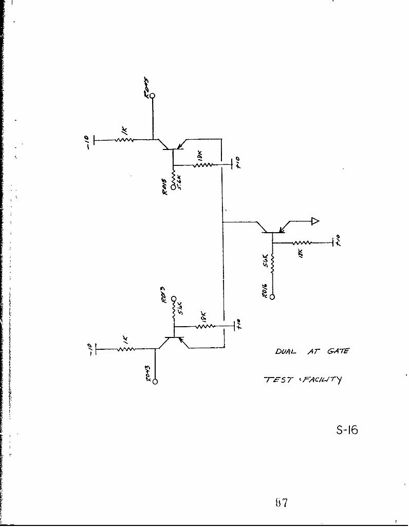
S-16 Dual AND Transistor Gate
S-18 Flip-Flop
S-19 Fractional Bit Delay Switch
S-20 Manual Delay Adjust
S-21 DCN, EF, and SW 10-2
S-22 On-Off Test Switch
S-23 Keyer Tuned Circuit
S-24 Keyer
iv
4
TABLE OF CONTENTS - PART II (Cont'd.)
Section
S-25 Mixer Amplifier
S-26 Band Pass Filter
S-27 Limiter Amplifier
S-28 900 Phase Shift Integrator
S-29 Driver Amplifier
S-30 Phase Detector
S-31 Low Pass Filter
S-32 Decision Circuit
S-33 Power Amplifier 1 and 2
S-34 Buffer Amplifier
S-35 Noise Feedback Band Pass Filter
S-36 Band Limiteed Noise Amplifier #l
S-37 Band Limited Noise Amplifier #2
S-38 Noise Amplifier
BD-A Test Facility Coding System
BD-B Block Diagram Coding
BD-C Rack Area and Circuit Designation Layout
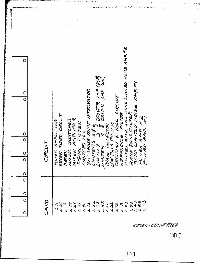
BD-D Keyer Converter Layout
BBD-l Clock Pulse Generator, Part 1 of 2
SBD-2 Clock Pulse Generator, Part 2 of 2
BD-3 Transmit Character Pulse Generator
BD-h Receive Character Pulse Generator
BD-5 Pattern Generator and Transmit Register
BD-6 Receiving Register and Comparators, Part 1 of 2
vC.
TABLE OF CONTENTS - PART II (Cont'd.)
Section
BD-7 Receiving Register and Ccmparators, Part 2 uf 2
BD-8 Mechanical C-inters
BD-9 Decimal Decoder and Meter Indicator
BD-I0 Test Fecility Counter Functions
BD-11 FSK Keyer and Converter
BD-12 Master Block Diagram
SIV
i''A
~vi

LIST OF FIGURES - PART II
Section
3.0 TEST FACILITY
Fig. 3.0 Test Facility Fnotograph
Fig. 3-.1 Pulse Sequence Tiagram
-Fig. 3.3 Keyer and Filter Table
Fig. 3.4 System Phase Table
Fig. 3.5 System Phase Characteristics
Fig. 3.6 Basic Phase Detector Wavefoiis
Fig. 3.7 Decision Circuits Waveforms
4. g
Fig. 4.1a Circuit Diagrams
Fig. 4.1b Circuit Diagrams
Fig. 4.1c Circuit Diagrams
Fig. 4.2a Band Pass Filter Characteristics
Fig. 4.2b Band Pass Filter Character'istics
Fig. 4.2c Band Pass Filter Characteristics
Fig. 4.2d Band Pass Filter Characteristics
Fig. 4.2e Band Pass Filter Characteristics
Fig. 4.2f Band Pass Filter Characamsritics
Fig. 4.3a Circuit Diagrams
Fig. 4.3b Circuit Diagrams
Fig. 4.4a Phase Detector Circuit
Fig. 4.4bo Phase Detector Circuit
Fig. 4.5 Phase Detectc'r Waveforms
Fig. 4.6 Phase Detector Cnaracteristic
vii
7
ILIST OF FIGURES - PART II (Cont'd)
Section
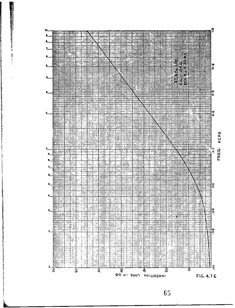
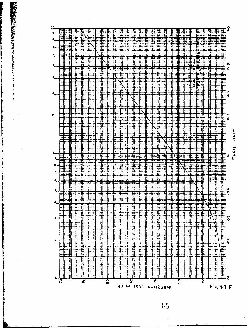
Fig. 4-.7a Low Pass Filter Curves
Fig. 4.-7b Low Pass Filter Curves
Fig. 4.7c Low Pass Filte! Curves
Fig. 4.7d Low Pass Filter Curves
Fig. 4.7e Low Pass Filter Curv3s
Fig 4.7f Low Pass Filter Curves
Fig. 4.8 FSK Converter Block Diagram
Fig. 4.9 Noise Feedback Control Block Diagram
Fig. 4.10a Wave Form Photos
Fig. 4.10b Wave Form Photos
Fig. 4.10c Wave Form Photos
Fig. 4-lOd Wave Form Photos
Fig. 4.11a Wave Form Photos--
Fig. 4.11b Wave Form Photos
Fig. 4.1-1c Wave Form Photos
Fig. 4.lld Wave Form Photos
Fig. 4 -.12a Wave Form Photos
Fig. 4.12b Wave Form Photos
viii

INTRODUCTION - PART II
The following pages, comprising Part II of the final report on
FAA/BRD-80 "Analysis of Advanced Data Transmission Tecaniques," consist
of detailed information relating to Sections 3 and 4 of Part i, according-
ly numbered Sections 3 and 4, and a supplementary group of schematics and
block diagrams designated Section 9. Part II contains no intervening
sections.
The report has been divided in this way tJ separate its total bulk
into two roughly equal parts and to improve its utility. For those prima-
rily interested in circuit design and layout and operating details relat-
ing to the Test Facility and experimental converters, Part II will serve
as a convenient reference.
Ic
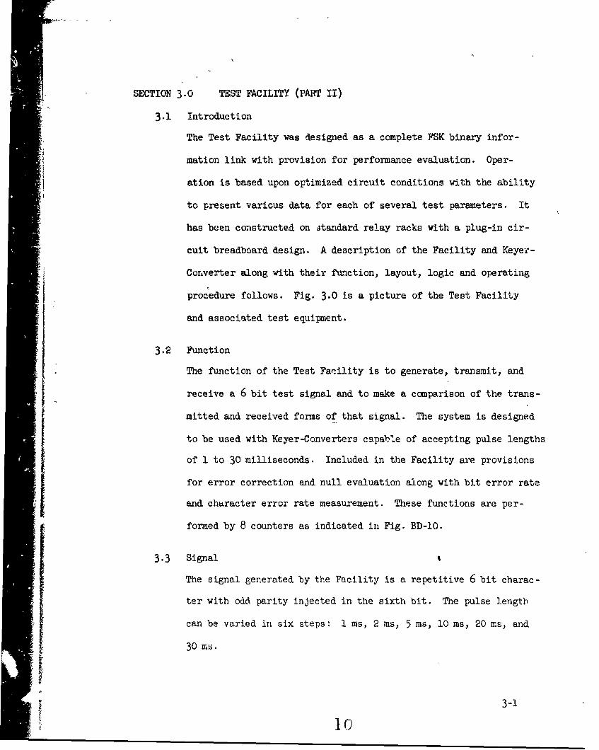
SECTION 3.0 TEST FACILITY (PART II)
3.1 Introduction
The Test Facility was designed as a complete FSK binary infor-
mation link with provision for performance evaluation. Oper-
ation is based upon optimized circuit conditions with the ability
to present various data for each of several test parameters. It
has been constructed on tstandard relay racks with a plug-in cir-
cuit breadboard design. A description of the Facility and Keyer-
Converter along with their fiunction, layout, logic and operating
procedure follows. Fig. 3.0 is a picture of the Test Facility
and associated test equipment.
3.2 Function
The function of the Test Facility is to generate, transmit, and
receive a 6 bit test signal and to make a comparison of the trans-
mitted and received forms of that signal. The system is designed
to be used with Keyer-Converters capable of accepting pulse lengths
of 1 to 30 milliseconds. Included in the Facility are provisions
for error correction and null evaluation along with bit error rate
and character error rate measurement. These functions are per-
formed by 8 counters as indicated in Fig. BD-I0.
3.3 Signal %
The signal generated by the Facility is a repetitive 6 bit charac-
ter with odd parity injected in the sixth bit. The pulse l.engtb
can be varied in six steps: 1 ms, 2 ms, 5 ms, 10 ms, 20 ms, and
30 ms.
3-1
" ~10

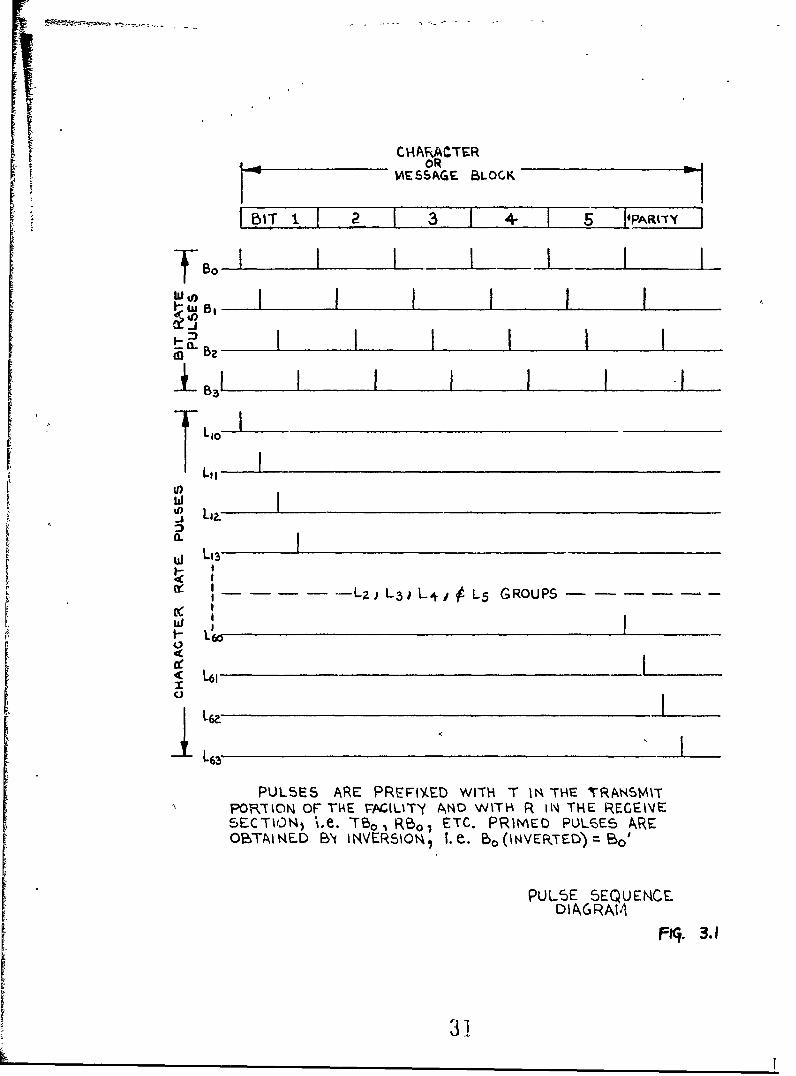
30 ms. The message can be selected for any mark-space code
by the 5 bit-selection switches. In addition to the message
block, transmitter and receiver timing pulses are generated
for use in the logic circuits. These pulses, along with their
position in respect to the signal, are shown ira Fig. 3.1.
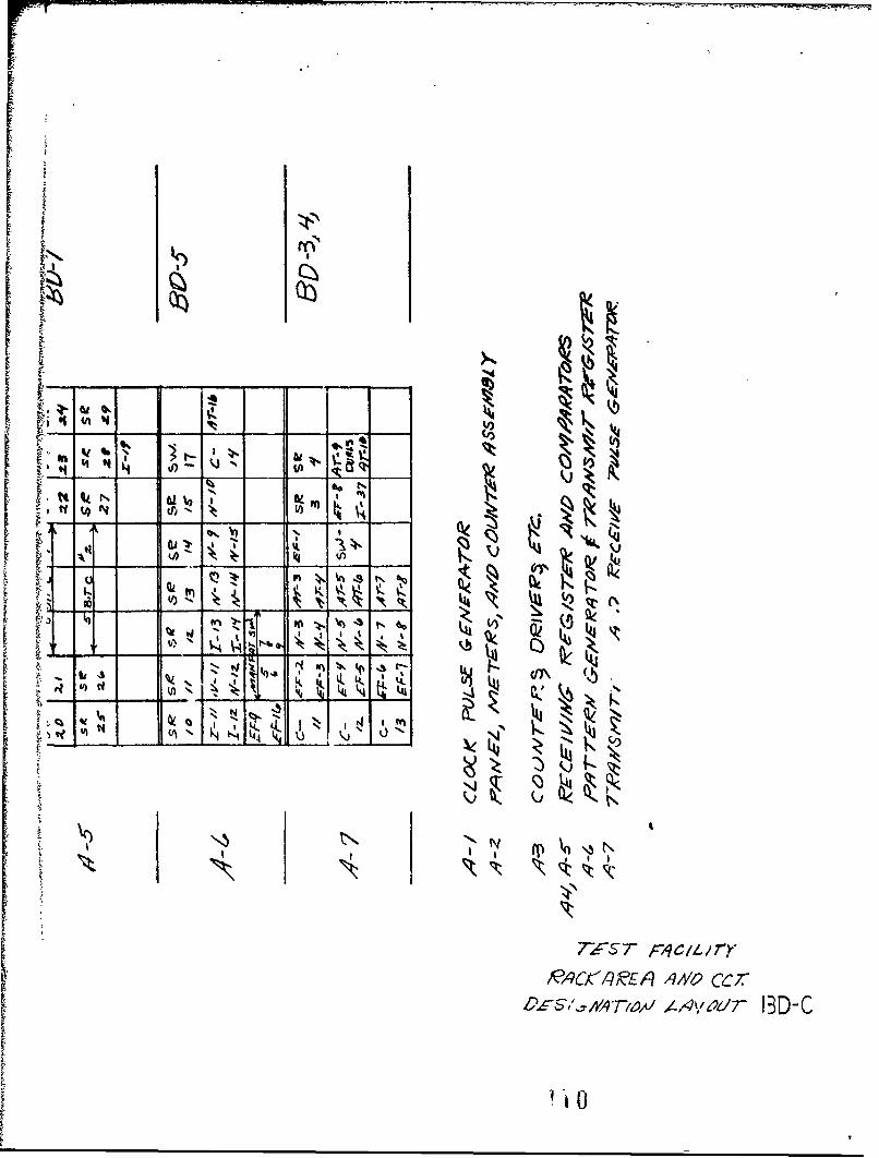
3.4i Layout
The Test Facility has been constructed on two standard relay
racks. Pictorial layouts appear in Fig. BD-C and Fig. BD-D,
showing rack area designations, their function, corresponding
circuit block diagrams, circuit and card functions, and lo-
cations.
The mair relay rack containing the Facility is designated by
areas coded A-1 through A-7. These areas include the clock
pulse generator, mechanical counters, shift registers and
comparators, pattern generator, and transmSt-receive pulse
generator. The auxiliary relay rack. is designated area A-8
and contains the optimized FSK Keyer-Converter portion of the
system.
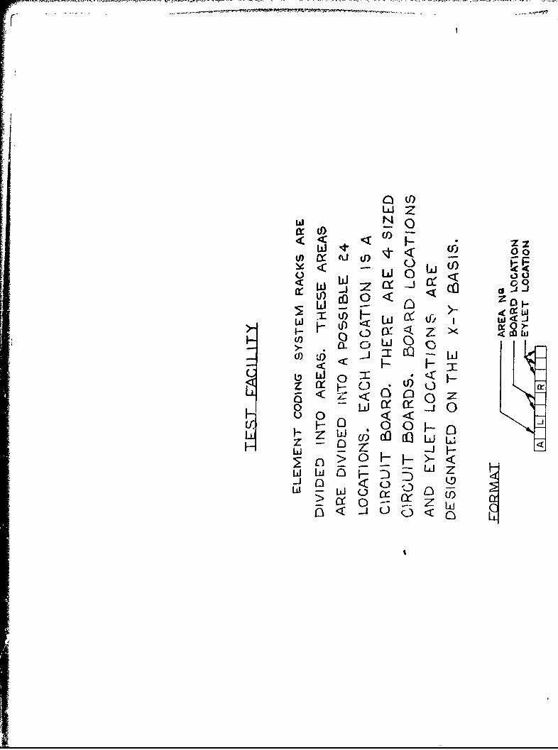
The Test Facility uses si-andard X-Y coding nomenclature for
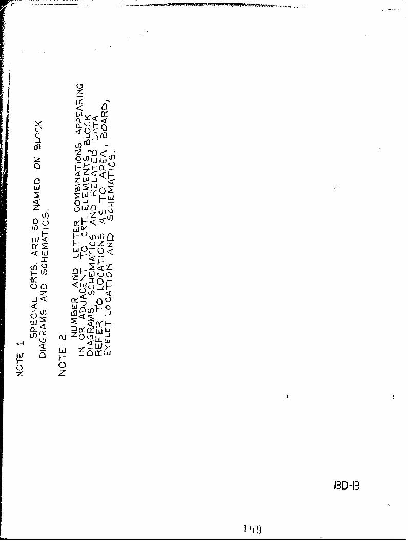
laeout location. See Fig. BD-A. Each eyelet, ocircuit board,
and area can be described by reference to a 9 digit code, based
on a combination of letters and numerals. Example designa-
tions are shown with their proper locations on the srea pic-
torial Fig. BD-A.
3-2
1'1
I
3.5 Diagrams
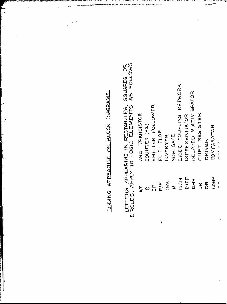
The operation of the Test Facility is covered ir the block
diagrams Fig. BD-l through Fig. BD-12. The coding of cirouits
on these block diagrams is given in Fig. BD-B. In addition,
area, location, and eyelet designations are given on each
block to facilitate locating circuits and circuit intercon-
nections. Each block is marked with a reference schematic
number "S", which refers to a schematic diagram in the sche-
matic section.
3.6 "ower Requirements
The Test Facility requires external DC power for operation.
The voltage and current requirements are as follows:
+ 10 volts @ 500 ma
- 10 volts @ 2 amps
In addition, an external audio noise source and an audio RMS
voltage reading instrument are necessary for hdjuisting SNR
ratios in the Keyer-Converter section for test purposes.
3.7 Facility
The operation of the Facility is covered in Fig. BD-12, a
Master Block Diagram of the Test Facility. Each major section
will be considered separately.
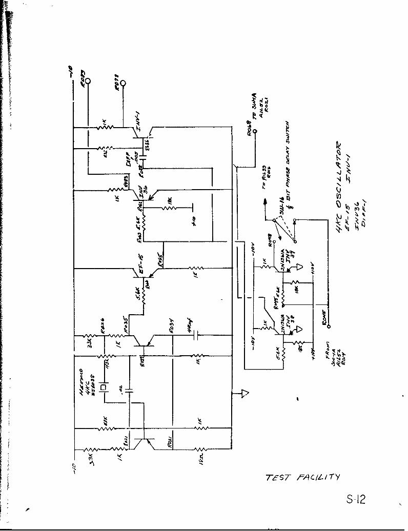
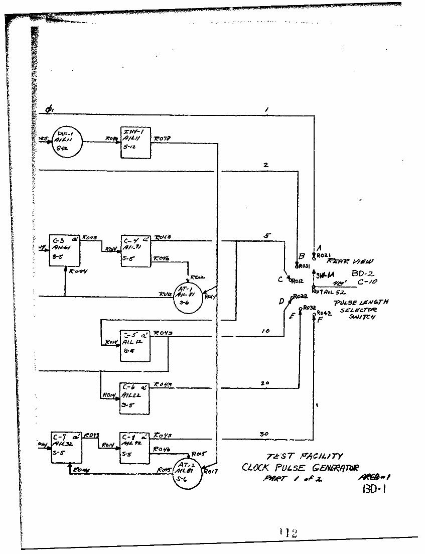
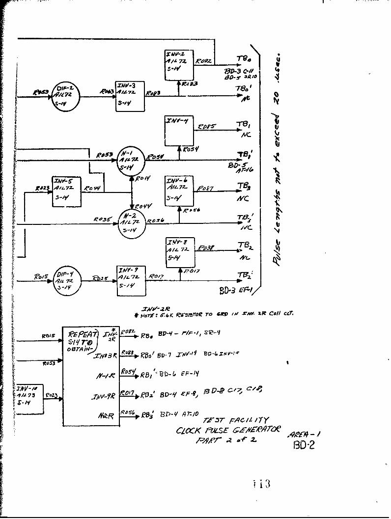
3.7.1 Clock Pulse Generator
The Clock Pulse Generator is located in Area A-1 aned
is covered on block diagrans in Fig. BD-1 and Fig. BD-2.
3-3IL
"The function of the Clock Pulse Generator is to create
a series of transmit and receive timing pulses with the
proper delays at six selectable bit rates.
The circuit operates from a stable crystal oscillator
(S-12) which produces 9 4 ke square wave output. The
pulse Length Selector Switch SW-lA selects this out-
put or a submulitple for use in creating the TB and
[ RB pulses. The TB pulses are formed directly by a
countdown of 4 and the proper differentiation, gating,
and inversion. The formation of the RB pulses is
identical with that of the TB pulses with the exception
of three input pulse delay ci-cuits.
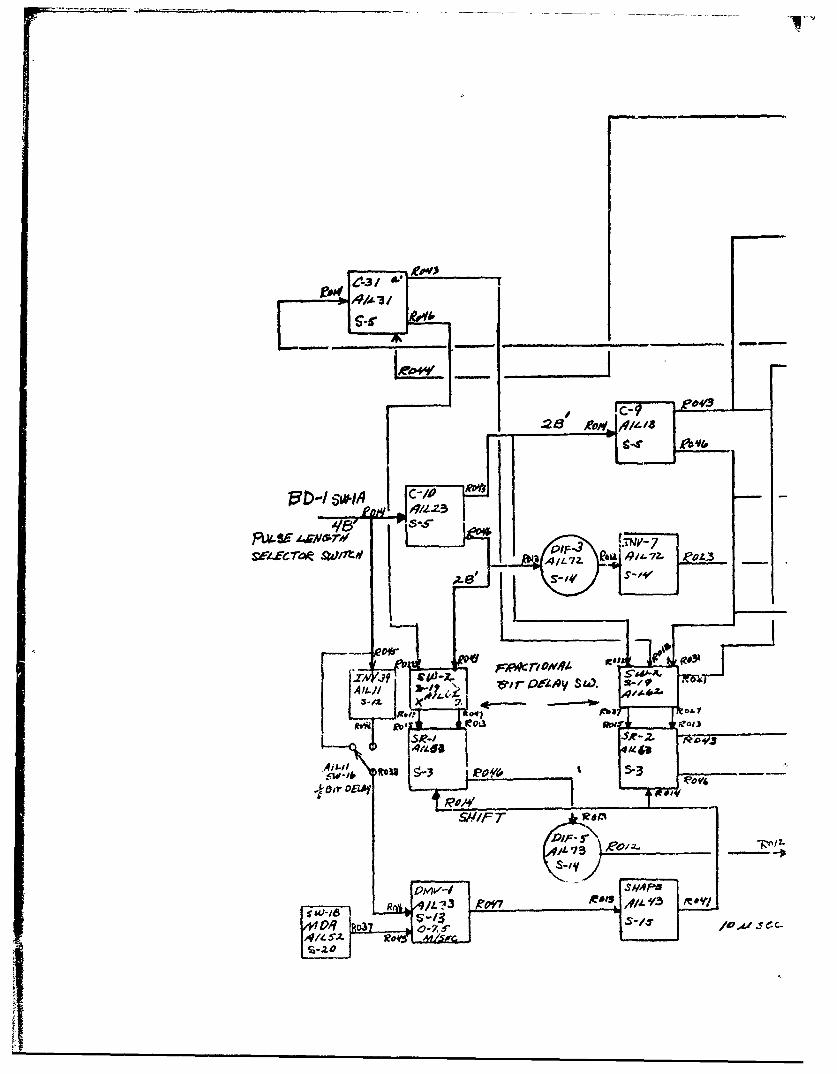
V [Fractional Bit Delay Switch SW-2 (S-19) controls the
input to Shift Registers 1 and 2, allowing the RB
pulses to be shifted in four 1/4 bit steps. The 1/8' Bit Delay Switch SW-16 (S-12) provides an additional
1/8 bit delay in all positions of the Fractional Bit
1. Delay Switch. The Variable DMV.-1 (S-13) is controlled
by the second section of (SW-1B), the Bit Length Se-
lector Switch, and has a vernier control continuous
delay of 0 to 7.5 milliseconds. The combination of
these delay circuits is sufficient to produce the
required delay in the receiving pulses to correspond
* with the delay in the Keyer-Converter used with the
system.
3-4I 1
The following bit lengths are generated in the system
with the Pulse Length Selector Switch in the position
indicated:
Position Bit Length
* 1 i ms
2 2
3 5
S4 10
5 20
6 30
The TB and RB pulse lengths do not exceed 20 micro-
seconds in any position of the Pulse Length Selector
[ Switch.
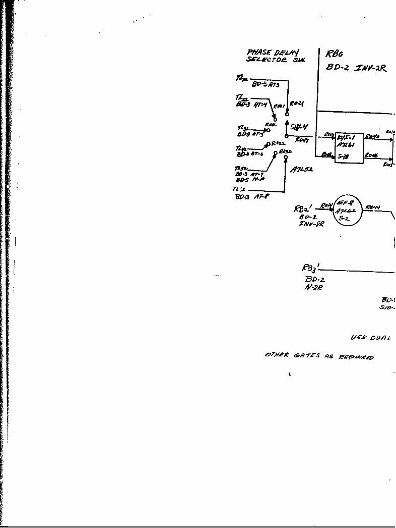
3.7.2 Transmit Character Pulse Generator
The Transmit Character Pulse Generator is located in
Area A-7 and is covered on the block diagram in Fig.
BD-3. The function of the Transmit Character Pulse
Generator is to create the TL pulses (Fig. 3.1) from
the TBo pulse.
The TBo pulse is sent through a series of 3 counters
and is NOR gated in 6 combinations. This result is
AND gated with TB to set the transmit TL pulses in2
the center of the selected bit. The outputs of the
generator are tied to SW-4, the Phase Delay Selector
3-5
I
Switch on BD-4.
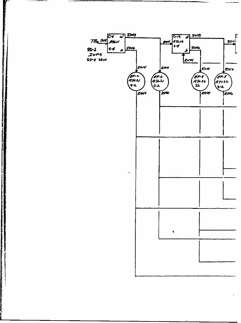
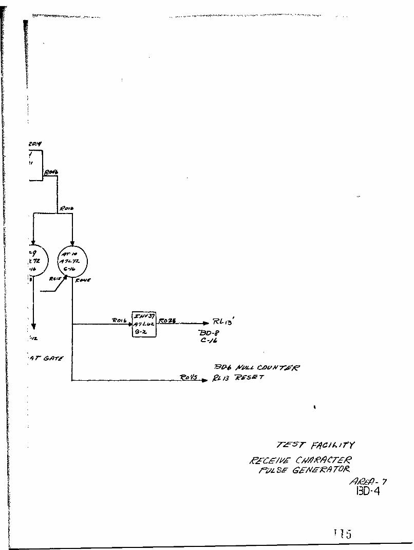
3.7.3 Receive Character Pulse Generator
The Receive Character Pulse Generator is located in
Area A-7 and is covered on the block diagram in Fig.
BD-4. The function of the Receive Character Pulse
Generator is to create the RL pulses frca the TL
pulses.
Phase Delay Selector Switch SW-4 selects a TL pulse
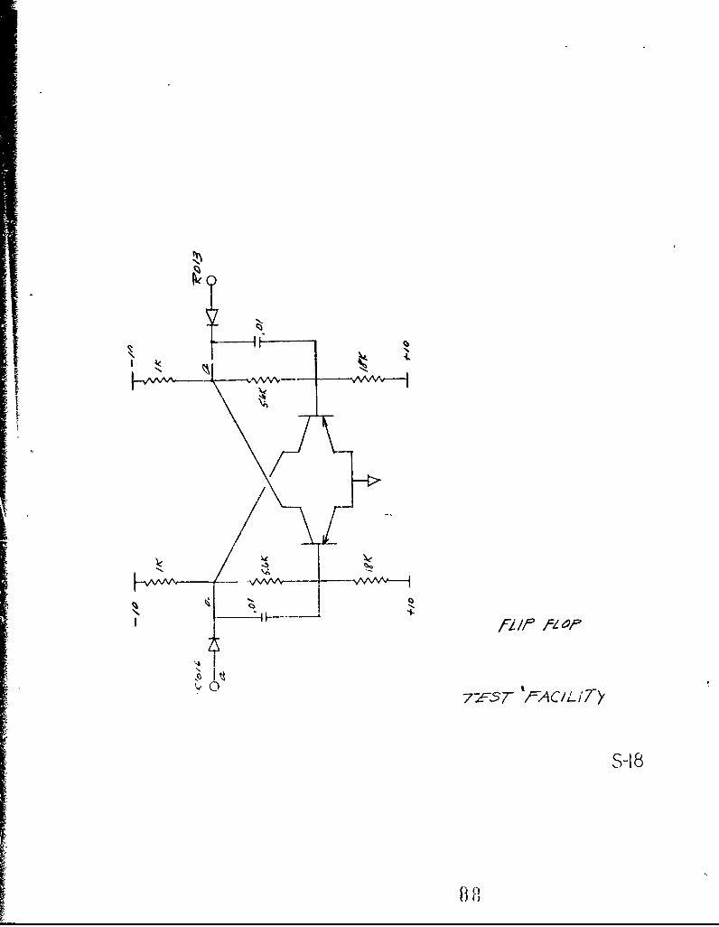
for triggering FLip-Flop-i (S-18). RBo is used to
reset F/F-l and shift the signal from Shift Register-4.
AND gating with the proper RB pulse produces the re-
quired character rate receive pulses. The Phase Delay
Selector Switch provides proper selection of system
character biming.
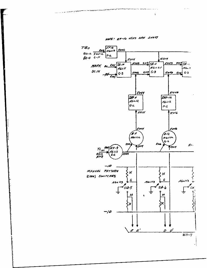
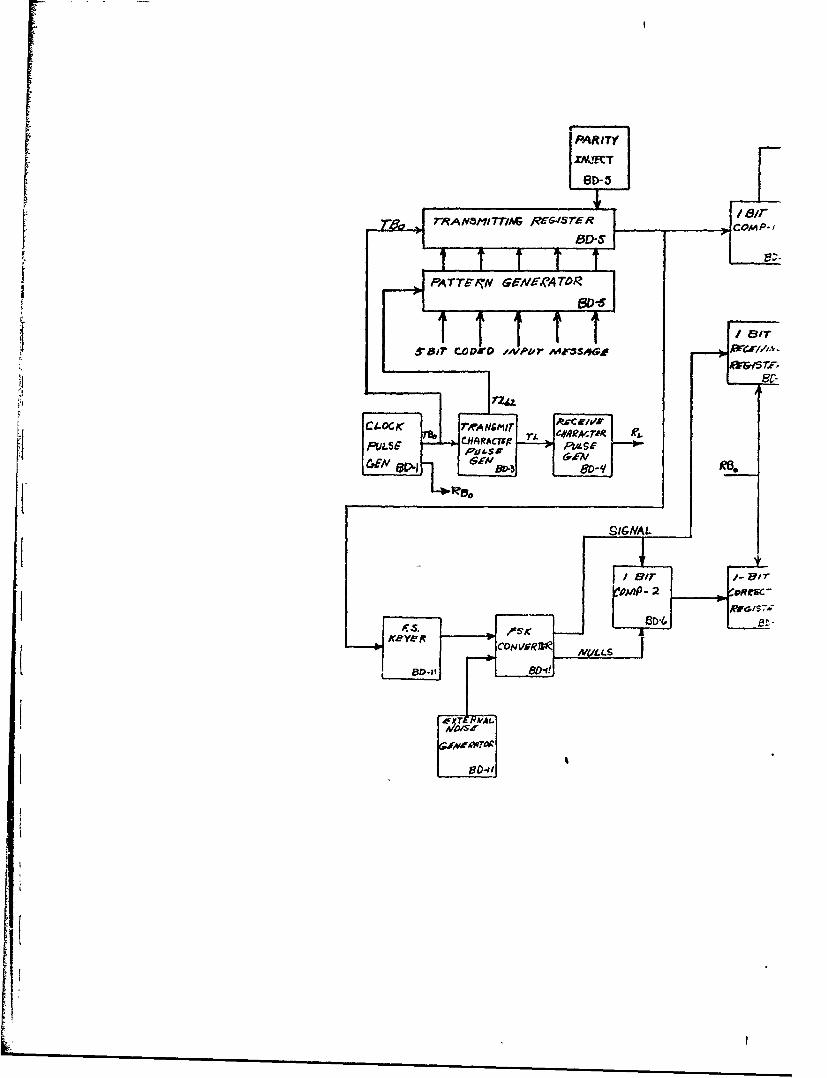
3.7.4 Pattern Generator
The Pattern Generator is located in Area A-6 and is
covered on the block diagram In Fig. BD-5. The
function of the Pattern Generator is to generate a
5 bit pattern and to inject Add parity in the 6th bit.
Manual pattern switches are provided to code into the
NOR gates a mark or space (ground or -10 volts). At
time TL6 2 these levels are gated and inverted and
passed into the Transmit %ift Register. Odd parity
(mark) is injected in the 6th time slot as a function
3-615
of Counter C-I4. The output of C-14 is sampled at
TL52 and gated into the Shift Register SR-15 at TL62,
which resets C-14 and reads the next cha 4ccer code
into the shift registers.
The outpu,; of the Pattern Generator Transmit Regis-
ter are sent to the keyer and 1 Bit Comparator-l. The
coded input levels are sent to the 5 Bit Comparators.
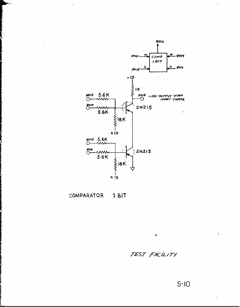
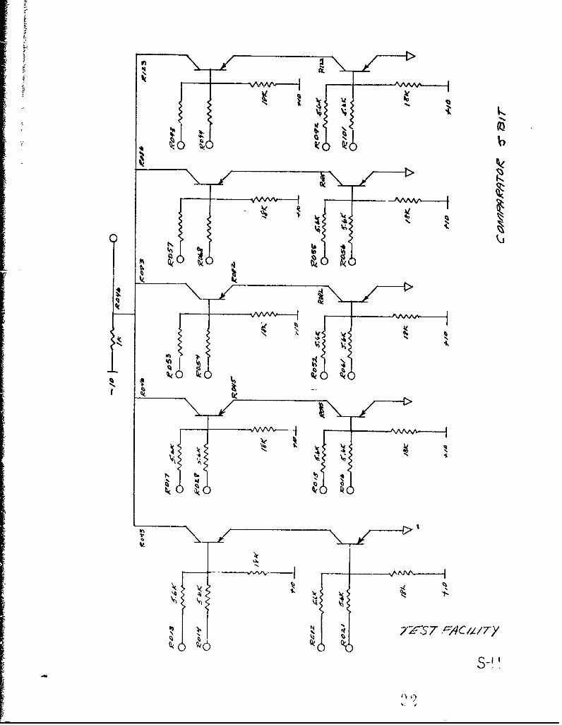
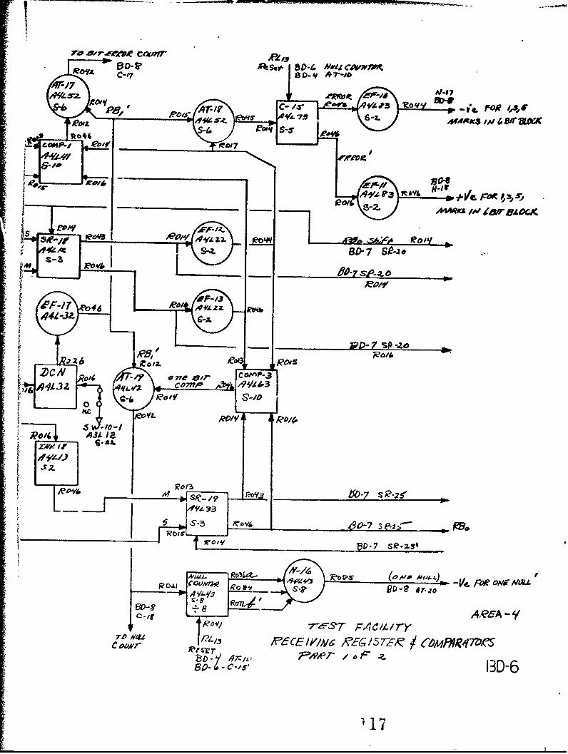
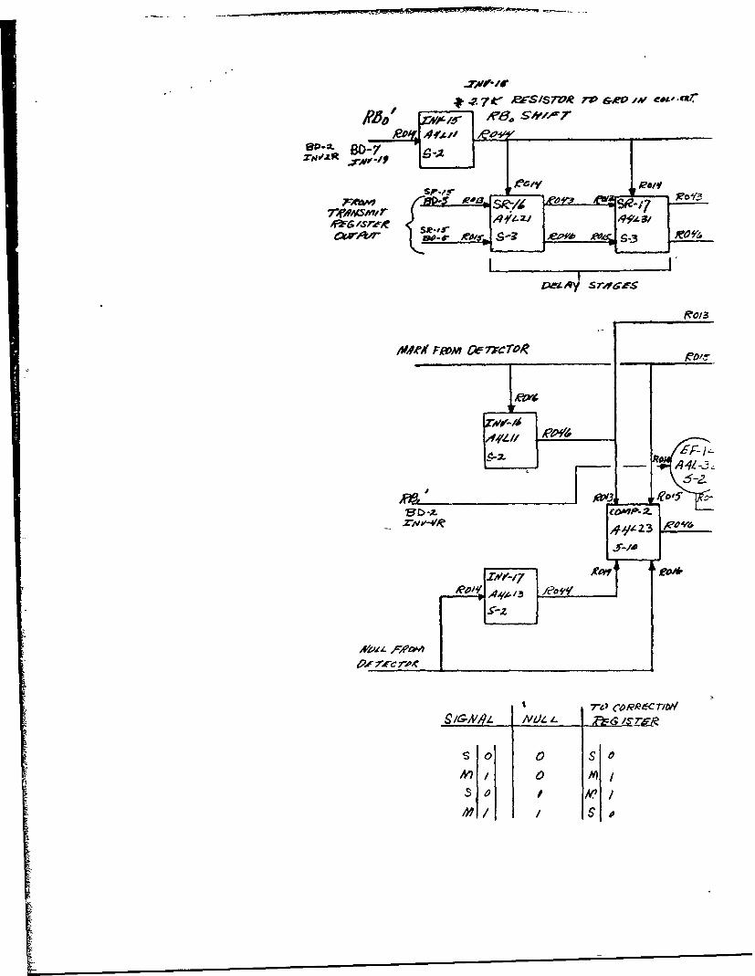
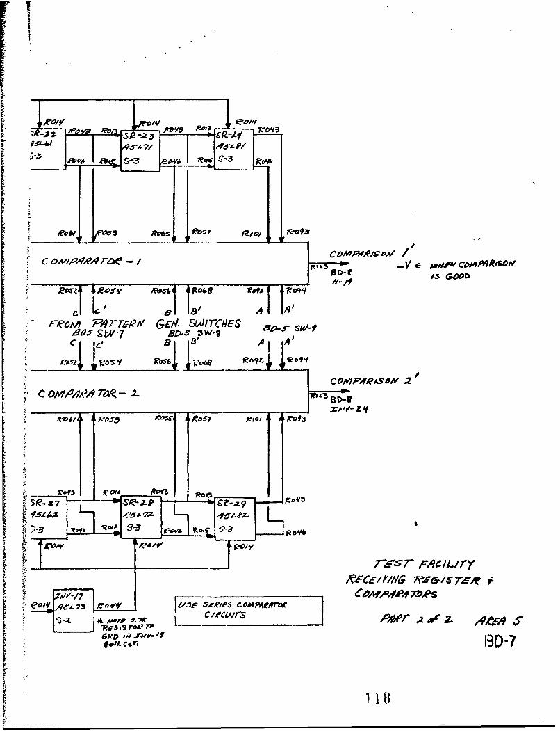
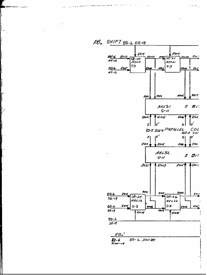
3.7.5 Receiving Register and Comparators
The Receiving Register and Ccmparatorf are located
in Areas A-4 and A-5 and are covered on block diagrams
Fig. BD-6 and Fig. BD-7. The function of the re-
ceiving registers is to place the incoming signal
timing in the correct phasing for comparison with the
transmitted signal and to provide logic outputs for the
various counters. The comparators receive the signal
from the receiving registers and compare it with the
transmitted code.
The signal from the detector (decision circuit) is
center sampled and shifted out of Shift Register SR-18
by RBo and into the receiving registertof 5 Bit Com-
parator-i. The output of this Comparator (COMP 1')
is negative when the comparison is correct.
If a null occurred d• :ing any bit the output of One
Bit Compa'ator COMP-2 will be inverted with respect
3-7
16

to the signal from the detector and this output will
be shifted through Correction Register SR-19 to the
receiving register of 5 Bit Comparator-2 by RBo. The
output of this Comparator (COMP 21) is negative when
the comparison is correct.
Null count logic is provided by IOOMP-3 output, sampled
at RB1 ' in AT-19. Bit error count is made by a one
bit comparison with the transmitted signal in COMP-I
and sampling by R1I 1 ' in AT-17. The number of marks
11 occurring are counted in C-15 and provide ERROR and
ERROR2 outputs. ERROR is negative for 1, 3, or 5F marks in a 6 bit block (odd parity check). A ONE NULL
signal is also provided from N-16 for use in the Me-
chanical Counter section.
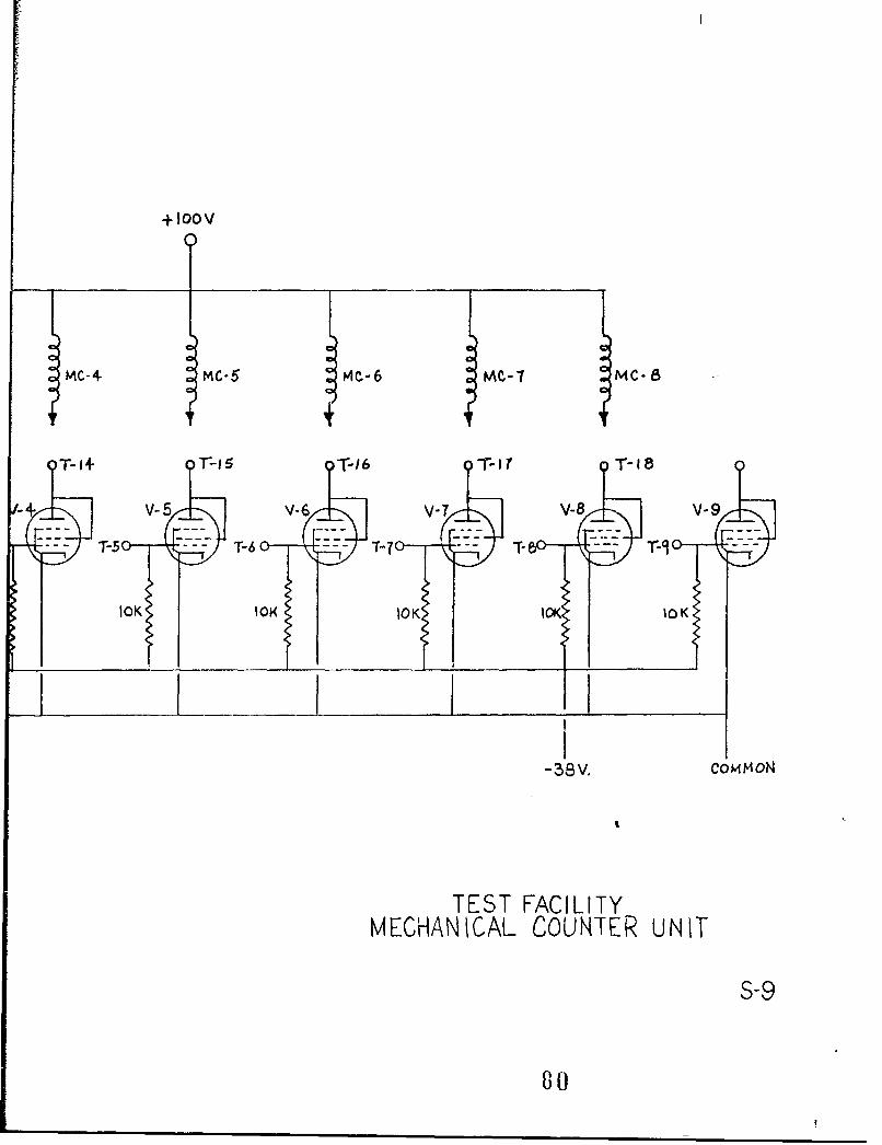
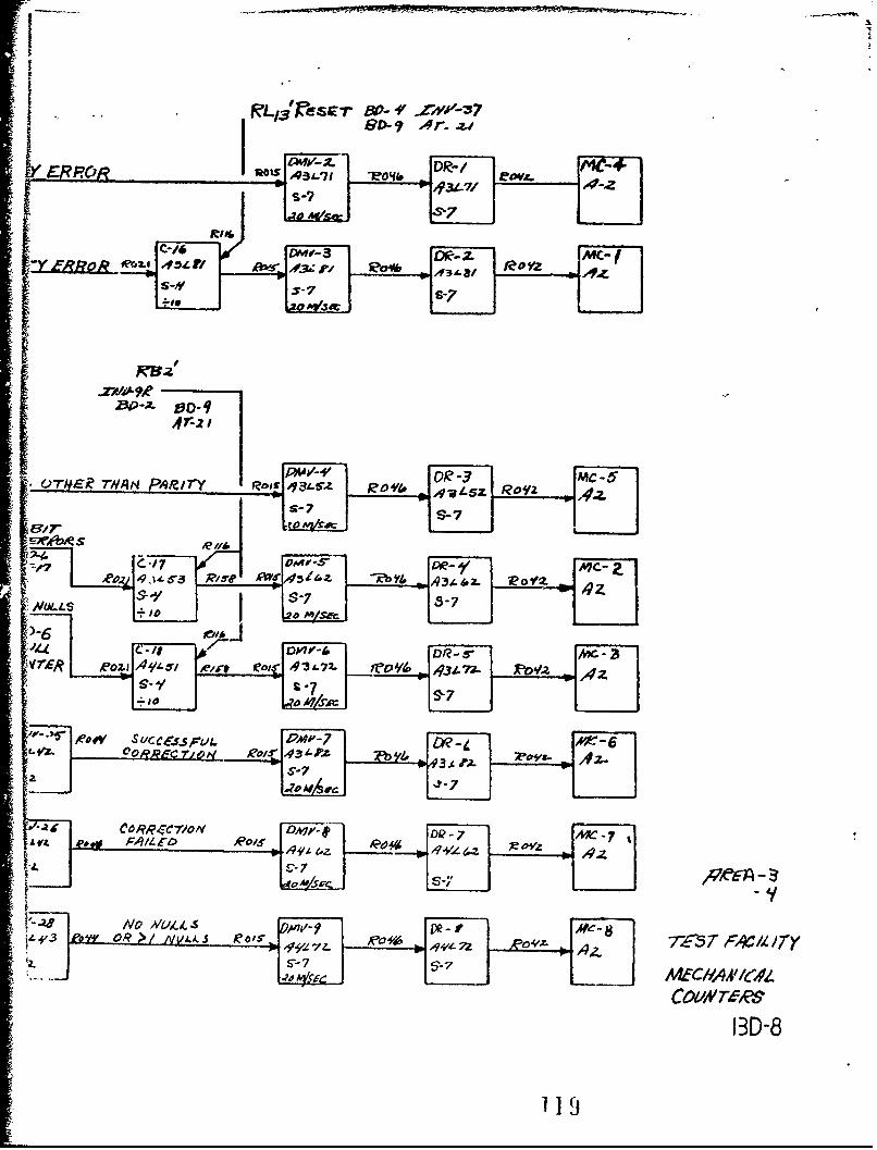
3.7.6 Mechanical Counters
The Mezhanical Counters are located in Area A-2. Their
associated logic and driving circuitry is located in
Areas A-3 and A-4. The circuitry is covered in the
block diagram on Fig. BD-8. The function of this
section is to count mechanically the various logic
circuit outputs.
%
The mechanical counter units opcrate in the plate
circuits of 35C5 pentodes (S-9). Each 35C5 is driver
by a 2N597 transistor driver (S-7) which operatez from
a DMV (S-7), furnishing f3 15 to 20 millisecond driving
3-817
wavc!fonm. Three Counters (MC-i, MC-2, and MC-3) con-
tain divide-by-lO counters on their DMV inputs for
high speed operation. The remaining counters have
direct driven DMV's. The mechanical counter unit has
a self contained Power Supply (S-i).
I The function of the remaining logic circuits can best
V be explained by consideration of the input requirement
for eacb counting operation separately in Counter
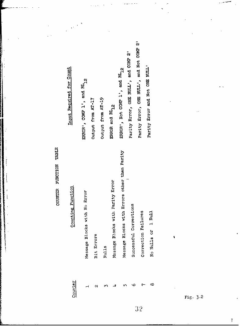
Function Table, Fig. 3.2.
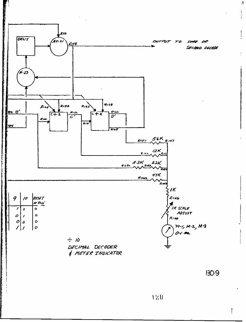
3.7.7 Divide-by-lO Decimal Decoder and Meter Indicator
The divide-by-10 Decimal Decoder and Meter Indicator
circuits are located in Areas A-3 and A-4 and are
covered on the block diagram in Fig. BD-9. The function
of this circuitry is to provide high speed operation of
Counters MC-1, MC-2, and MC-3 by dividing the inputs by
10 and providing a units readout meter.
The counters operate with the logic as indicated in the
logic diagram on Fig. BD-9. Automatic reset is pro-
vided by RL1 3 '1 A momentary toggle switch is provided
for manual resetting. Readout currentg are controlled
by individual fixed resistors in the counter outputs
A', B', C', and D'. A meter adjust vernier is provided
to control the meter current to give approximately
linear indications.
3-918
3.8 Facility Logic and Counter Functions
The Facility logic is shown in Fig. BD-10. Counter locations
are given in the pictorial provided. Reference should be made
to Master Block Diagram, Fig. BD-12, and Counter Fanction Table,
Fig. 3.2, for a complete analysis of system operation.
The ten counting functions shown in Fig. BD-1O are performed
by 8 mechanical counters and two simple arithmetic calculations.
If tests are being performed at high bit rates and low SNR ratios,
electronic counting must be used to supplement the mechanical
counters for accurate count. These may be connected into the
system at the inputs to DMV's 2 through 9. See Fig. BD-8.
3.9 Facility Operating Procedure
The following operating procedure covers the Test Facility
V• Areas A-1 through A-7 and all controls located therein. It
assumes a complete and fuActioning Keyer-Converter, as described
in Section 3.10 of this report, and proper input and output
connections to the Facility.
1 - Apply power to all circuits by operating the ex-
ternal supplies and the self-contained mechanical
counter supply in A-2.
2 - Select the proper pulse length for transmission
with Switch SW-I (AlL52).
3 - Salect a message on the 5 bit Code Selection
Switches SW-5 through SW-9 (A6L23). See pictorial
on Fig. BD-5.
3-10
i7
4- Adjust 1/4 Bit Delay Switch SW-2 (ALL62), 1/8 Bit
Delay Switch SW-16 (AIL1UR056), amd variable con-
trol on DMV-1 (AIL33R033) for center sampling of
the received signal by RBo at SR-18 (AfLl2), using
an cscilloscope to monitor the adjustment.
5 - Adjust Phase Delay Selector Switch SW-4 (A7L52) for
RL1 3 reset at Counter C-15 (A.L73) to occur during
the parity (6th) bit. (Note: Proper adjustment
of SW-4 will permit only Message Blocks with No
Error (MC-1) to count with a noise-free signal from
the detector and a message other than alternate mark-
space).
L 6 - Switch SW-1O is provided as an ON-OFF Test Switch
(A3L12) and should be operated to start and stop
the test.
7 - Switch SW-17 (A6L71) should be placed in keyed po-
sition for Test.
The Facility is now properly adjusted for Keyer-Converter evalu-
ation, Supplementary checks and adjustment of Counters C-16,
C-17, and C-18 can be made with the controls ?rovided (R156 on
Divide-by-lO Counter) for proper digits read-out on Counters
MC-1, MC-2, and MC-3. All counters should be reset with the
switches provided before each test.
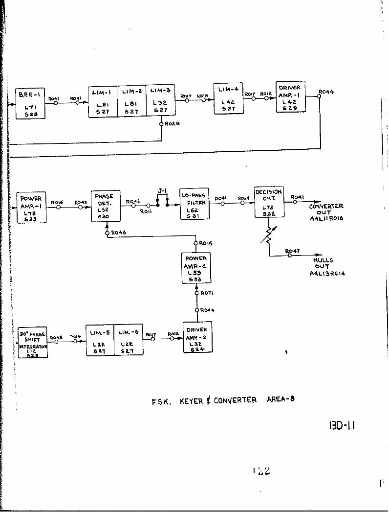
3.10 Keyer and Converter
The Test Facility is provided with a complete matched set of
3-1120

tone keyers and optimized converters located in Area A-8. The
circuit parameters are based on those discussed in General
Dynamics/Electronics-Rochester Preliminary Report for Task I
and Interim Repoiu for Task II, "Analysis of Advanced Data
Transmission Techniques," Section 5.1.
A block diagram of the Keyer-Converter is shown in Fig. BD-11.
The series of plug-in units provided will adapt the unit for
operation at 6 different bit rates. Fig. 3.3 presents the
pertinent keyer and filter data for the test parameters. Each
block of Fig. BD--11 is referenced to a schematic "S" number.
Interconnections are shown on Fig. BD-11.
An external noise generator and RMS reading voltmeter must be
used with the system for evaluation.
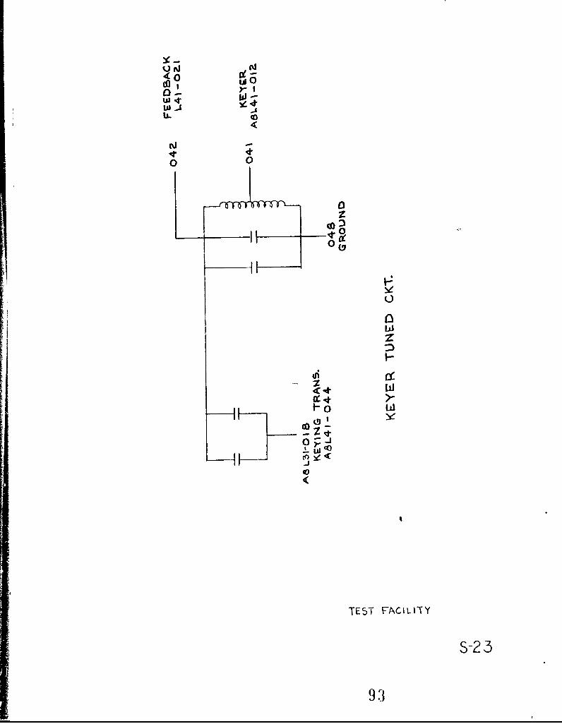
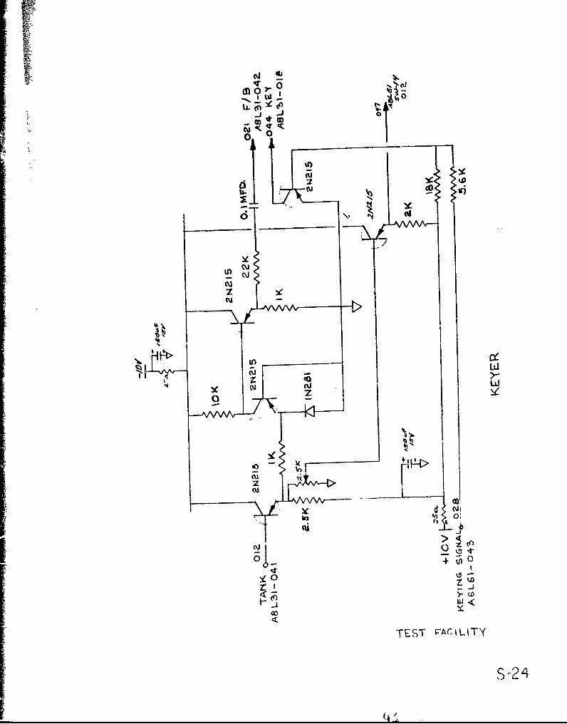
3.10.1 Keyer4 The Keyer, shown on Schematic S-24., is a feedback
oscillator with provision for accepting plug-in tankcircuits (S-23). The tank circu.ts are so constructed
that a keying signal (-10 volts) into the keyer will
short the keying capacity to rGround and so lower the
frequency of oscillation. Voltage feedback stabilizes
the keyer output. Six tank circuits are provided with
the Keyer (Fig. 3.3) and tre tuned to give optimum per-
formance and balanced converter outputs.
3-12
21

3.10.2 Band Pass Filters
Two identical Band Pass Filters are provided for each
bit length (Fig. 3.2) and their basic configuration is
shown on Schematic S-26. These filters serve two pur-
poses in the operation of the converter.
Band Pass Filter #1 follows the Mixer Amplifier and
defines the system bandwidth, rejecting all noise com-
ponents outside this band. The design criteria for
this filter will be discussed in Section 4.
Band Pass Filter #2 follows Limiter #3 and provides a
matched phase characteristic with that of Filter #1 at
the center of the passband (within 20). In addition,
Filter #2 contributes a phase shift characteristic
throughout the band which contributes to converter
operation by establishing a reference channel.
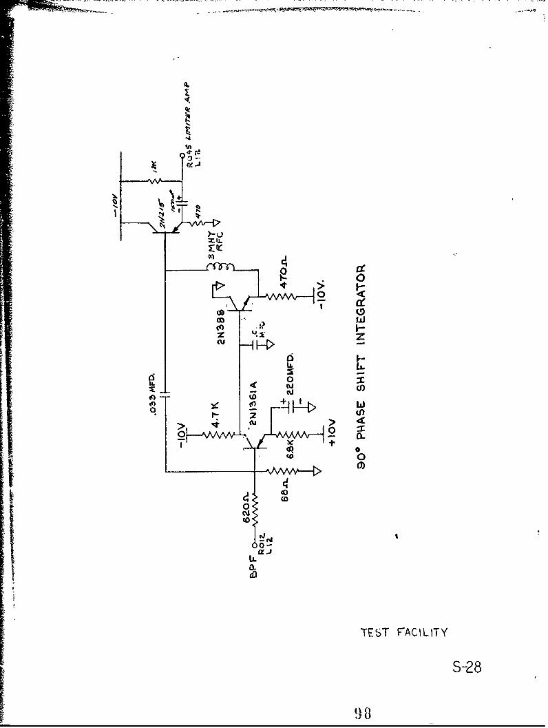
5.10.3 900 Phase Shift Integrator
The 900 Phase Shift Integrator (S-28) is a modified
operational amplifier with capacitive feedback. This
amplifier provides a constant 900 phase shift over the
frequency of operation, thereby ccmpleting the phase
shift necessary in the reference channel for driving
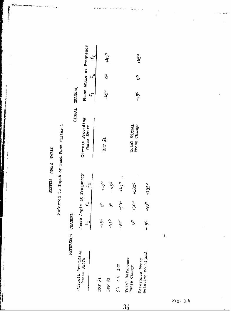
the phase detector. The system phase table of Fig. 3.4
explains the phase relationship between the signal and
reference channel after the signal has passed through
3-1322
the band pass filters and che 900 Phase Shift Integ-ator.
Fig. 3.5 shows the phase detector drifing waveforms for
center frequency and the two keyed frequency conditions.
3 .i10. 4 Limiter Amplifiers
The Limiter Amplifiers (S-27) provided with the con-
verter are operated in cascade to provide a high system
¶ gain. Each Limiter is an operational amplifier with
voltage feedback in each section to provide a large dy-
namic range of input fo-r a constant square wave output
amplitade of approximately 1 volt peak-to-peak. The
LimiTers provide gain sufficient to operate the con-
{. verter with input levels (measured at the output of BPF #1)
of less than 1 millivolt.
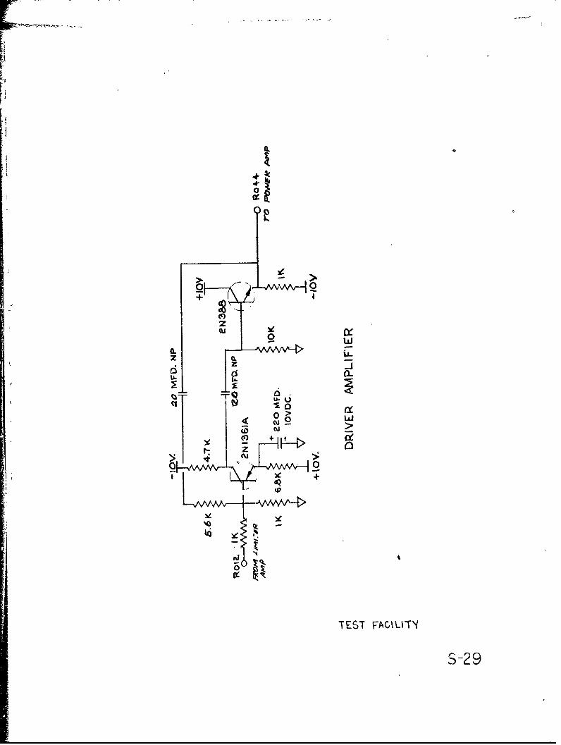
3.10.5 Driver Amplifiers
The Driver Amplifiers ,S-29) receive the outputs of the
Limiter Amplifiers #4 and #6 and boost this waveform to
an amplitude of 7 volts peak-to-peak for use in driving
the AC coupled feedback power amplifiers.
3.10.6 Power Amplifiers %
The Power Amplifiers (S-33) used in the converter are
transformerless complementary symmetry feedback amplifiers
capable of furnishing a 4 volt peak-to-peak driving wave-
form into the 8 ohm primary winding of the phase detector
tiansformer. Peak powers of over 250 milliwatts can be
23-14~2 3

provided during detector conduction cycles. The output
gain control is in the feedback loop.
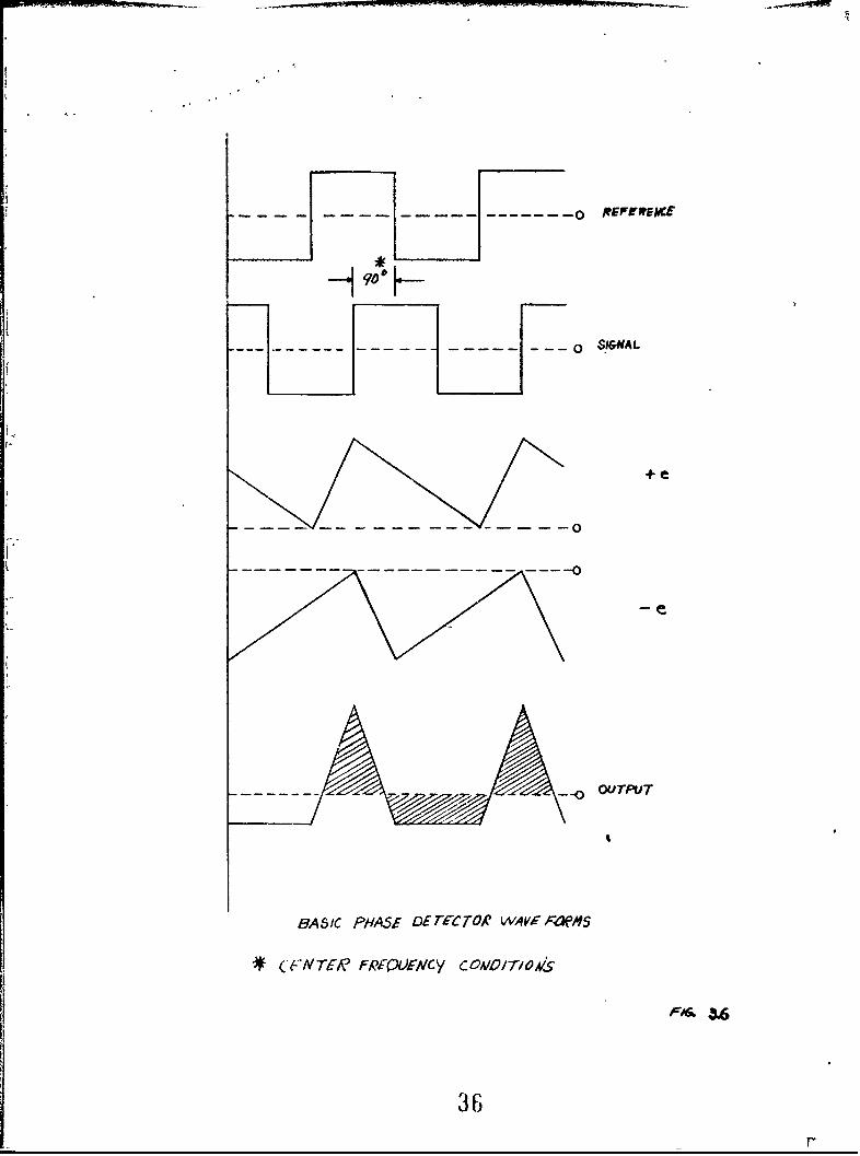
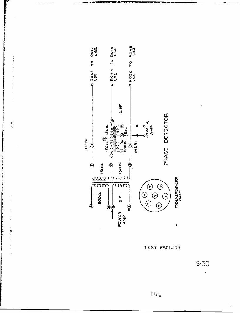
3.10.7 Phase Detector
The Phasep Detector (S-30 and S-17) combines the signal
and reference channels by transformer coupling in a
manner to provide diode conduction on a positive going
reference and signal waveform combination. fig. 3.6
shows the basic detector waveforms for a center Zre-
quency condition. Phase detector outputs are obtained
by the net difference in voltage developed across C1 and
C2 (S-17) over the period of a bit. This integrated wave-
form is referenced to + 5 volts and adjusted (gain control
on the Power Amplifiers) for t 5 volts output in respect
to this reference. The reference waveform is maintained
at an amplitude greater than one-half that of the signal
waveform.
3.10.8 Low Pass Filter & Emitter Follower Driver
The Low Pass Filter (S-31) is driven by the phase detector
and its output is referenced to + 5 volts. Six plug-in
Low Pass Filters are provided for operation at each pulse
length (Fig. 3.3). The Emitter Followers (S-32) provide
isolation and current gain for drIving the decision cir-
cuitry without shifting the reference potential signifi-
cantly.
3-15
24
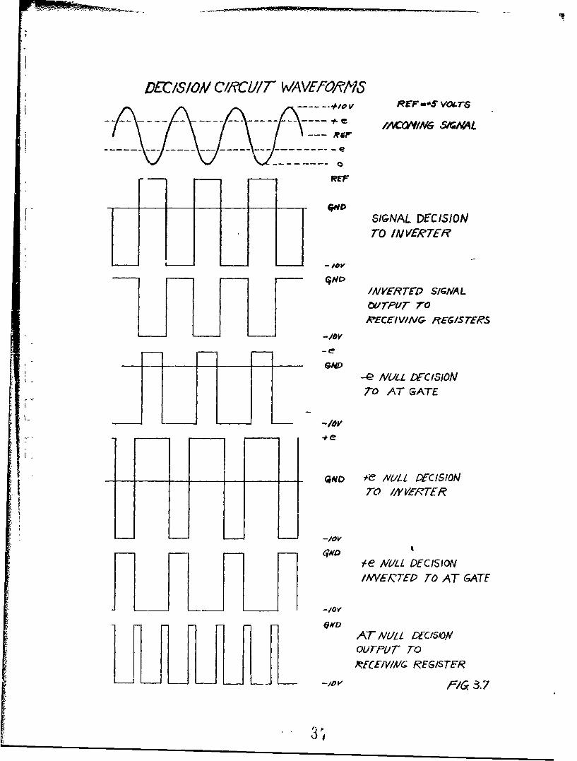
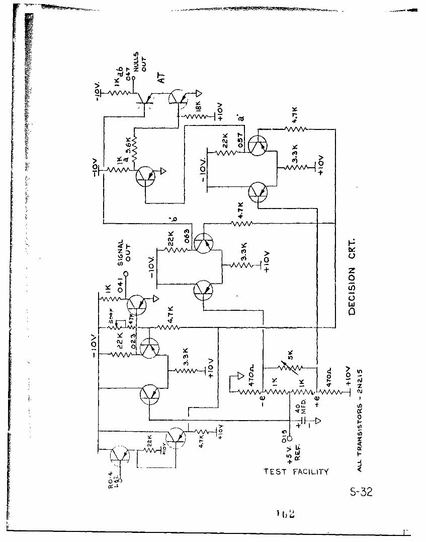
3.10.9 Decision Circuit
The Decision Circuit (S-32) is designed to provide a mark-
space (Gnd. or - 10 volts) output, switched each time the
incomi::g waveform crosses the reference potential (+ 5 volts).
Fig. 3.7 shows the waveforms present in the decision cir-
ouitry on an alternate mark-space code. In addition to a
signal -,.itput, the decision circuit has an adjustable null
detection network, which provides an output (Gnd.) when the
signal fails to pass a preset level (positive or negative
in respect to the reference voltage). Signal and Null out.-
puts are used to drive the receiving regir.cers where they
are center sampled Dy RBo.
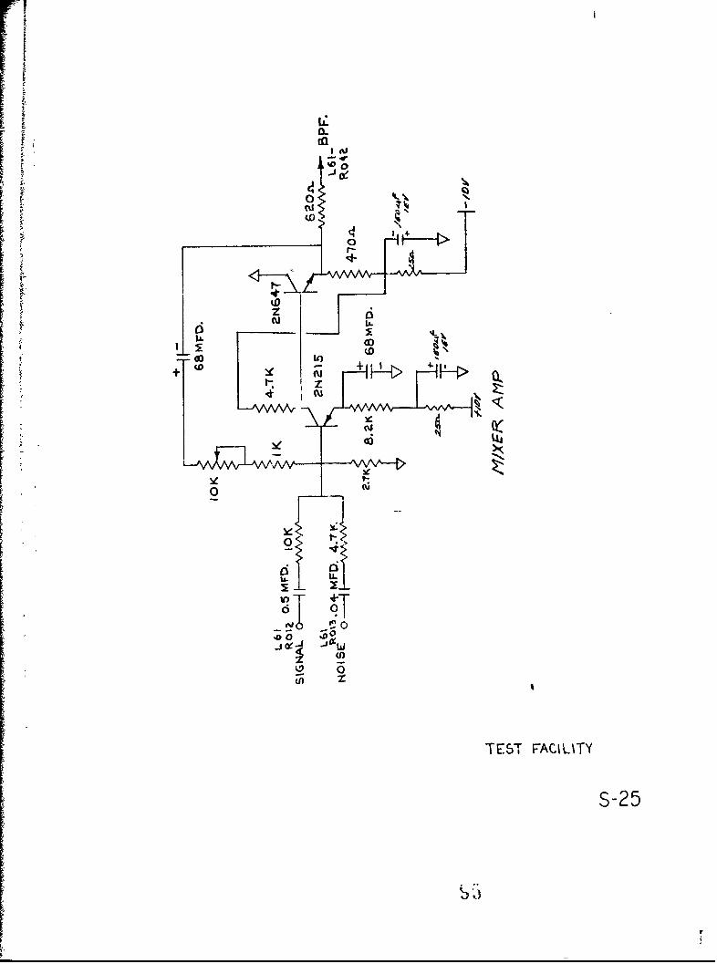
3.10.10 Mixer Amplifier
V" The Mixer Amplifier (S-25) provides a means of mixing noise
and signal and the- necessary isolation for SNR measurements.,
¶ Switches SW-14 and SW-15 (Fig. BD-II) select noise or sig-
nal inputs separately. The mixer gain control is located
in the feedback loop and controls the amount of signal and
noise driving BPF #1.
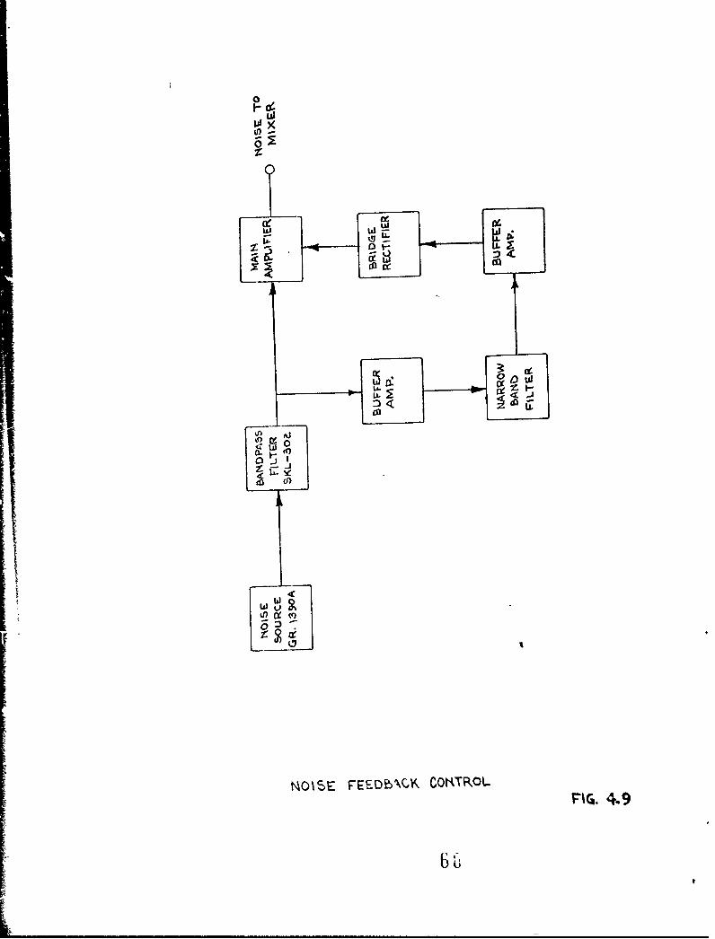
3.11 Noise Feedback Control
An external noise source must be used with the keyer-converter to
provide a white noise spectrum for SNP evaluation of the system.
H• General Radio Random Noise Generator type 1390B or similar type
audio noise source is recommended for use ith the system.
I The noise source should be fed through an external bandpass filter
SB3-16
S25

adjusted for a passband of t 1.2 kc at the center frequency used.
'The output of this filter is fed to the BNC connector input of the
Noise Amplifier on A8Lll as shown on Schematic S-38. This high
gain amplifier has been shielded and decoupled to provide maximum
isolation from supply line transients, associated circuitry, and
stray fields.
The noise input to the amplifier must be sufficient to provide a
nominal feedback voltage of 1.7 volts at point "X". A typical in-
put using the GR 1390B is 2 volts, read on the instrument output
meter. A feedback loop is provided to stabilize RMS noise amplitude
without destroying the Gaussian characteristics of the noise.
A noise output, obtainea at A8LllR086 and fed through a banana
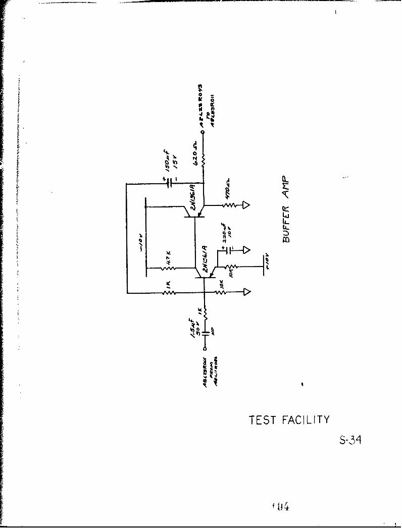
Jack R051, is amplified by the Buffer Amplifier (S-34) on A8L23
with its input on R015. The output of this Operational Amplifier
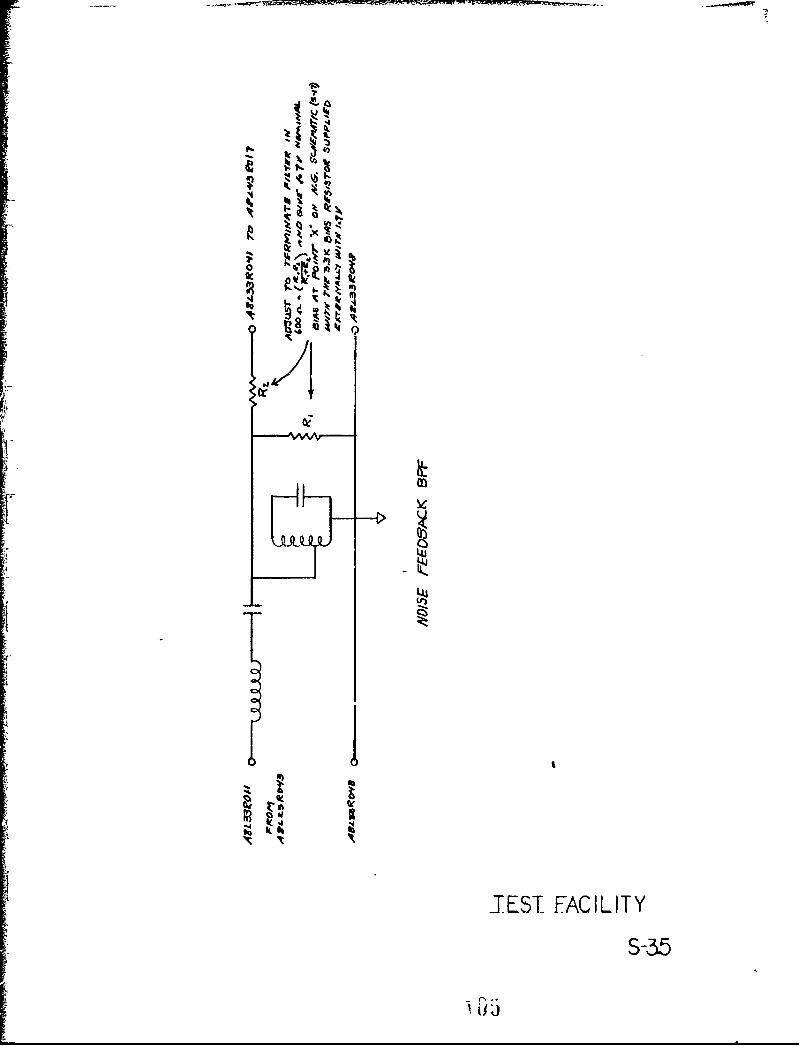
(R043) is fed through a Bandpass Filter (A8L33). Four filters
(S-35) are provided for this function. They are used as follows:
Noise Filter
Pulse Length Center Freq. Bandpass
1 ms 8 kc 900 c/s
2 4 450
5 1.6 190
10 1.6 190
20 1.6 47.5
30 1.6 47.5
The Noise Feedback Filter output is fed to Band Limited Noise
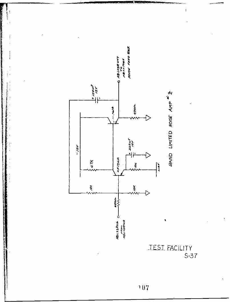
3-1726

Amplifier No. 1 (S-36) (A8L.3R017), and its output (R028) is
taken to Band Limited Noise Amplifier No. 2 (S-37) (A8L23Rol6).
Both amplifiers are operational amplifiers. The output of
Amplifier No. 2 (RO47) is taken to R065 via banana plug ROIl and
transformer coupled to a Bridge Rectifier (S-38). The WC out-
put of this rectifier is filtered by a long time constant L-C
network and DC coupled to an emitter-follower. The output of
this emitter-follower is point "X" and provides a feedback
voltage, which is a function of the noise in a limited pass-
band.
Results show that this system of noise control appears to be
the only feasible means of making long term narrow band noise
measurements. A Flow Corporation Random Signal Voltmeter type
12A1 was used for noise measurements. This instrument has a
time constant of 16 seconds.
No gain controls are provided in the noise control system.
After adjustment of noise input level from the noise source
for the nominal DC feedback voltage at point "X", all measure-
ments are based on the existing noise level present out of the
Mixer Amplifier.
3.12 Ke'er and Converter Operating Procedure
The Keyer and Converter are supplied with six sets of plug-in
cards for operation of the system as indicated in Fig. 3.3.
These plug-in units consist of the following:
3-18
27
1. Keyrr Tuned Circuit
2. nTo Identical Band Pass Filters
3. Low Pass Filter
Each of the circuits has been adjusted for optimum conditions
under actual operation and test. The phase detector RC time
constant has been included on the Low Pass Filter card and
has been selected to minimize non-linearities existing in the
system under noise conditions. The keyer tuned circuit has
been adjusted to provide a specified shift and a reference
(+ 5 volts) output, from the phase detector on alternate mark-
space code.
The following procedure should be followed to place the Keyer-
Converter into operation or in changing Prom one set of plug-
in units to another:
1. Place plug-in cards in their proper positions as
follows:
Position Card
L 31 Keyer Tuned Circuit
L 71 Signal Filter
L 13 Reference Filter
L 62 Low Pass Filter
2. Apply power to the system.
3. With Jumper J-1 removed adjust the decision circuit
for reference (+ 5 volts) output (A8L72Ro4l).
4. Adjust the variable null control (A8L72R026) for
3-19
2 C

the null width desired by measuring between R015 and
Ro16.
5. Adjust the amplitude of the output of Power Amplifiers
#1 and #2 to provide t 5 volts (with respect to the
reference) at the output of the Low Pass Filter w..th
switch SW-17 (A6L71) in mark and space positions, re-
spectively (maintain reference output greater than 1/2
signal output). Return this switch to keyed position
after adjustment has been completed.
6. Connect an audio noise source to the BNC connector pro-
vided on LlI through an external bandpass filter with
a bandpass of t 1.2 kc/s of the center frequency of
operation. Using the correct Noise Feedback Filter
in L33, (see Section 3.11) adjust the noise source out-
put to give 1.7 volts DC at point V'" in the Noise Ampli-
fier.
7. Adjust the Test Facility as instructed in Section 3.9.
Measurement of SNR ratio can be carried out at the output of Band
Pass Filter #1 (A8L7mo4l) with a long term averaging RMS reading
voltmeter. Amplitudes can be controlled by the output control on
the keyer and mixer. It is advisable, however, since input noise
levels are limited by the feedback loop, to set the mixer control
fully clockwise (maximum) and to adjust SNR ratios by using the
keyer output control. Switches SW-14 and SW-15 are provided for
convpnience in making system measurements. These switches apply
signal and noise independently to the mi>er amplifier.
2 3-20

40 -At-- - -
al
I It.U-.-
.uVWA~ftVl_3l
C f4 MrACTER
MAESSAGE BLOCK
!.•' 1~ 2• I 4 5 s [PA,,,,,
•'"BIT_T ,Bo
L) IIIII"W Be
II
%LIZ:- ~ L• :L5GOPa.
13-
< tL6
SI .
'L
L6,"
PULSES ARE PREFIMED WITH T IN THE TRANSMITPOR'•tON OF TkE VAGILl"' AMiD WITH R IN THlE REGEIV/E
SECTION) l.e. Tbo, R.,o ETC. PRIMED PULSES AREOBTAINED BM INVER$ION, i. e. %o(INVERTED')= Bo'
PULSE 5EQUENCE.DIA&GRAMI
pF. 3.1
31
0
43 ' C3
E) cm d f$4 H --I
$+4 ms~
4) 0
-H Id4$4 $
o -ft
o cmO~0
$4
00
$4 $4
$ 4 3.
0~~
4' 4ý' 4 -) 4' 3
M 0ci ~ )0 . 0 rz4
H ) r1 I 0 0
0~$ 4 to
W~ $4 b U) .-
U) d U) W)~
V) 4' H U) ~ ~ $
Wt -4 ~ ) C 1 0 0
H- N\ (n .. i'. \ t- CO
0C) Fig. 3.2
3

43 t
to, LL\ t (
N4 0~ LIN~ H r.
0
p.4
.0
0, 0
0 R8 8' o- U
04 00 0 t\0
C) 0 r vrI -
PI 0 0 0 Or)
[\ ,.'\ 0 0 0
,41)44,
Fi.0-
C) 33
4 u 0 0
(D+ +
4,Ci 0 0
pp. 4 0 0
4)0 0
0 r
4H H - -,
-r4 4 awto)
cir
mt
0 0 0 0 0
04 + + + H H4-) 4 + +
co 0 0 00 C) 0\ 0 00 H 0\ +00
C-) 0
++
> co (f)
4- 0(C)* 0 C" ,pq m~ 0\ EH f1r
Fig. 3.4

SiG
RE[F
SIG
SYS 5TEIA PHASE C/IAA'ATENGIG'5T
,F/G. 3.5
S- --- SIGNAL
+-e
----- - - - - OuTPUT
aA5 IC PHIIASE DEMTC TOC WAVE 1,2(','f
S('6N TFRb- FPFQL)AWC COA/V/7Y0,/S
36
DCC/S/O// CiNCl1F7 WA V~fO/'?/ki6tRET -ALS VIM T6
-~~~c /ACfiN &iZ4%
REF
SIGNAL DECISIONTO /At VERTFl?
IN VERTEPh S/GA(AL
A'ECCIV/NG /?/ZW/?SMP
-'Dv
-e NULL DECISION710 AT GATE
____rov --A NV_- eIVL LCECISIONTO /A1Z'CTER
F1 Ile N11IL1 DECIS ION
L /NVVE/'7TEP TO AT GATE
AT A/tLL 4605161//
OUTpUT ToLK111111 FCE/V/A1(; REGIS TER

SECTION 4.0 CONVERTER DESIGN (PART II)
4.1 Introduction
The converter section (Fig. 4.8) of the Test Facility was designed
to test the predictions of Montgomery 3 and to provide a set of opti-
mized data at each of six pulse lengths. In order to accomplish
this task, it was necessary to provide keyers able to accept an in-
put code and generate an FSK signal with the prescribed frequency
shift. A source of white noise was also necessary to correlate
the results with predicted performance. A highly de-,ailed analysis
of t'e converter is outside the scope of this report; presented
in this section are some of the more important design considera-
tions.
14.2 Converter Operation
Signal and noise can be selected individually by Switches S1 and [n
(Fig. 4.8) and their levels measured at point A, where the values
of signal-to-noise power ratio in the system bandwidth are defined.
After three stages of limiting, providing gain at low input levels
squaring action at high inputs, the signal splits into the sig-
nal and reference channels. In the signal channel more gain is
provided through another limiter, a driver amplifier, and a power
amplifier to drive the signal winding of a phase detector. In the
reference channel the phase shift filter alters the phase of the
signal, causing lead or lag of a magnitude proportional to the
difference between the signal frequency and the center frequency
of the phase shift filter. The reference signal now paszes through
4-1
I
an integrator, which produces a 900 phase shift in the reference
signal, and, after two stages of limiting, it is applied through
a driver amplifier and a power amplifier to the reference winding
of the phase detector.
At center frequency the signal and reference square waves are 900
out of phase at the input to the phase detector and there is no
output. As the frequency moves above and below the center value,
Sthe phase shift in the reference channel vari-:,s and the detector
output will go positive and negative, accordingly. A low pass
filter removes the carrier and a decision circuit centered about
zero output frcm the phase detector gives mark or space output, as
the frequency at the input varies above or below the center fre-
quency.
4.3 Converter Circuit Design
4.3.1 The Mixer Amplifier
In order to perform converter SNR measurements, a circuit
was required to mix signal and noise in a linear manner so
that each one could be measured separately and then added
to obtain the combined effect without change in the measured
value of either. The mixer amplifier was required to drive
a bandpass filter with a purely resistive source impedance
of 600 ohms. These requirements led to the selection of an
ope-ational amplifier (Fig. 4.1A) to sum signal and noise.
Fig. 4.1B shows the amplifier taodifVea for use a, a mixer.
Fig. 4.1C shows the basic circuit of the operational amplifier.
S4-2
This amplifier will supply voltage gains of 20 db, which
are independent for signal and noise. The output impedance
is of the order of 1 ohm and, therefore, the use of series
resistance provides ideal matching for all loads.
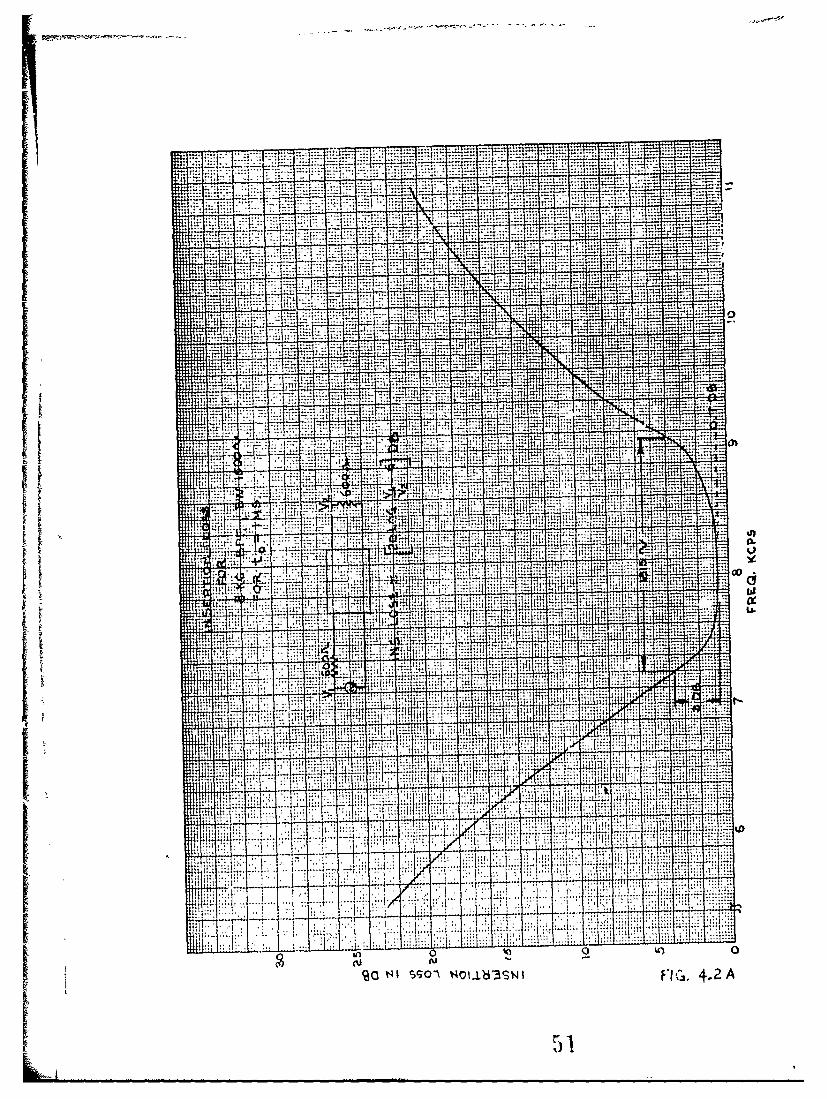
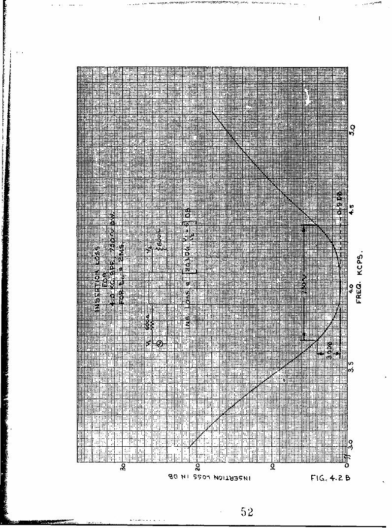
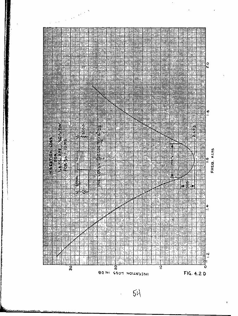
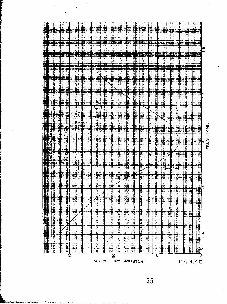
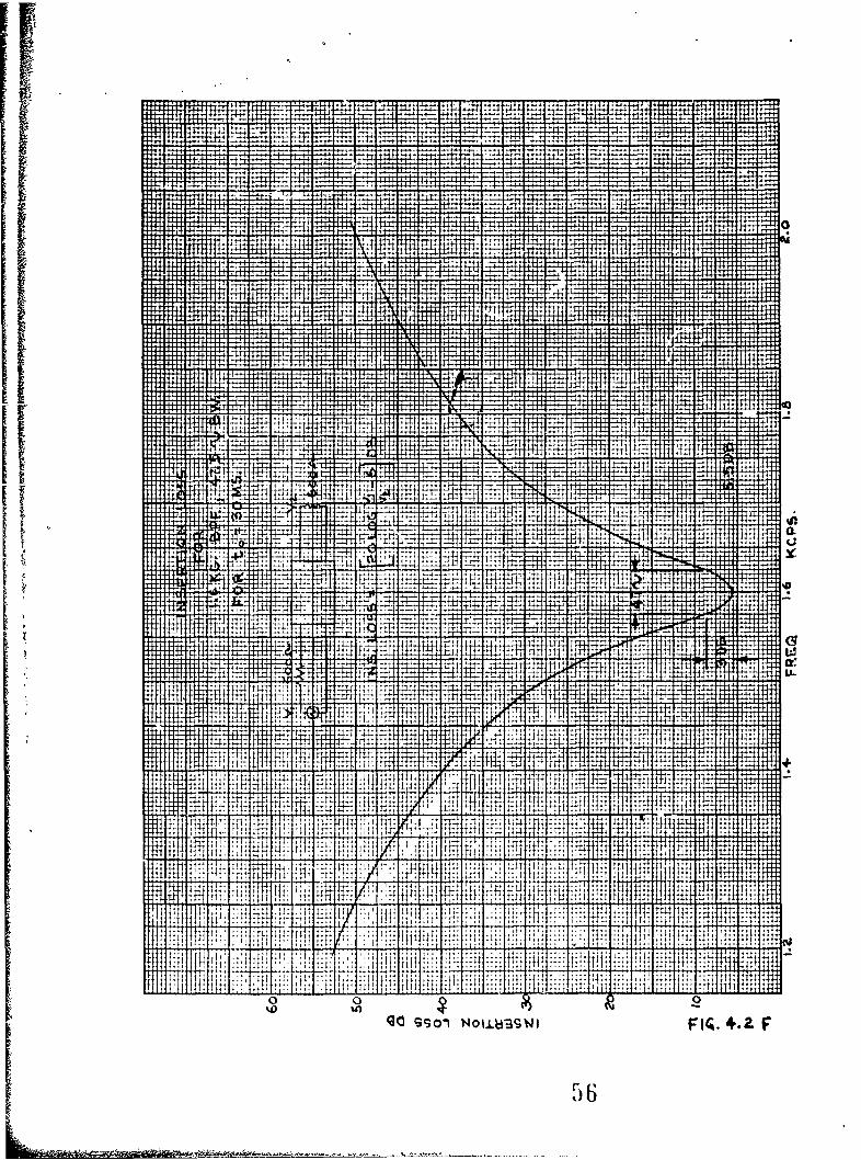
4.3.2 The Bandpass Filters
Fig. 3.3 shows a table of date pertinent to the design
specifications of the bandpass filters. Section 4.3, Part I,
discusses the design criteria for these filters. The response
characteristics are shown in Fig. 4.2A through Fig. 4.2F. The
filters (S-26) are two branch L-C units with bandwidths shown
on each curve to the 3 db points. These filters provide phase
shift characteristics of t 900 across the bandpass. The first
bandpass filter of Fig. 4.8 defines the noise bandwidth of the
converter and maximizes SNR ratio. The second bandpass fil-
ter is matched to within 20 of the first and establishes areference phase (Fig. 3.4).
4.3.3 Limiters
The function of a limiter amplifier in an FM system is to
remove amplitude variations from the received signal. Two
requirements for a limiter are operation bver a wide range
of input voltages and mainten-ince of a symmeLrical waveform
over this dynamic range. A circuit which meets these require-
ments is a modified operational amplifier with a non-linear
feedback network, consisting of two diodes in parallel with
opposite polarity. Fig. 4.3A shows the basic circuit con-.
4-3
figuration.
The diode selected for the feedback network was chosen for
a minimum forward voltage drop change for a given change in
current. The 1N81.6 diode used for this function exhibits
a forward voltage change of 0. volts to 0.8 volts (2X) for
a change in current from 10 microamps to 10 milliarips (1000K).
At very low levels the circuit acts as a P'imple amplifier.
As the input is Increased, limiting starts to take place and
with further increases very little change in peak-to-peak
output will occur. The slope of the leading and trailing
edge of the waveform will increase to the limit of the cir-
cuit elements when limiters are cascaded. These amplifiers
are responsible for the sensitivity (less than 0.5 millivolts
at all pulse lengths) and wide dynamic range (70 db voltage
gain) of the converter.
The function of the integrator in Tche converte.r is to pro-
vide a fixed 900 phase shift throughout the freq~uency range
of operation. The basic operat'",onal amplifier with a capaci-
tive feedback loop was selecteei to perforqi this function.
Fig. 4.3B shows a schematic of this amplifier. Rl was made
equal to 600 ohms to terminate the filter correctly, and
l/W C was made equal to 600 ohms at 8 kc, giving unit gain
at that frequency and a gain of 5 at 1.6 kc. The phase shift
through the integrator was within 20 of 900 over the frequency
44-
range of operation.
4.3.5 Driver and Power Amplifiers
The output of the limiter amplifiers after squaring is only
1.2 volts peak-to-peak, which is inadequate to drive a
saturating transistor stage directly. The driver amplifiers
were designed for use at this point in the system to provide
a gain of approximately 6 and an output centered about
ground. The power amplifiers are ccmplementary-symmetry
emitter-follower output devices with the ability to furnish
a 4 volt peak-to-peak output into 8 ohms for driving the
phase detector.
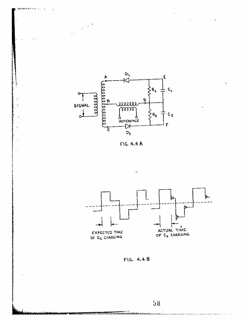
4.3.6 The Phase Detector
The phase sensitive detector is shown in Fig. 4.4A with
reference symbols. Fig. 4.5 presents wave form diagrams for
a square wave input, total signal and reference amplitudes,
ana a linear charge and discharge characteristic assugmed for
the capacitors. As the phase of the reference Fnd signal
changes from the 900 (center frequency) condition depicted,
longer or shorter charge and discharge times will anply for
the Capacitors Cl and C2 , and a net DC level change in the
output E with respect to F will take place in an amount
proportional to the phase change. Transformer coupling is
necessary in a detector of this description for two major
reasons: (1) to provide a step-up and sumning effect large
enough to give the desired output voltage swing and (2) to
,*4-5
enable the insertion of a convenient reference voltage
level on the output.
An investigation of the circuit after design showed some
peculiarities of loading on the power amplifiers. It was
determined that Capacitors C1 and C2 were continuing to
charge long after such charge should have ceased. Fig.
.4.AB shows a sketch of the expected voltage function and
the actual voltage function observed at point A when point
D is grounded. Ringing shown was due to lack of load on
the transformer and is apparently not detrimental. The
reasons for the effect shown were not immediately obvious,
but experiment showed that a reduction in the capacitive
load cut down this excess charge time. Too small a ca-
f pacity was undesirable since the maximum voltage would
then be reached with an exponential curve. A compromise
of values was effected so that near-linearity was obtained
with very little excess ciarge time showing. The excellent
linearity of the resulting phase detector is shown for one
set of parameters (30 ms) by the oatput voltage vs. fre-
quency input curve in Fig. 4.6.
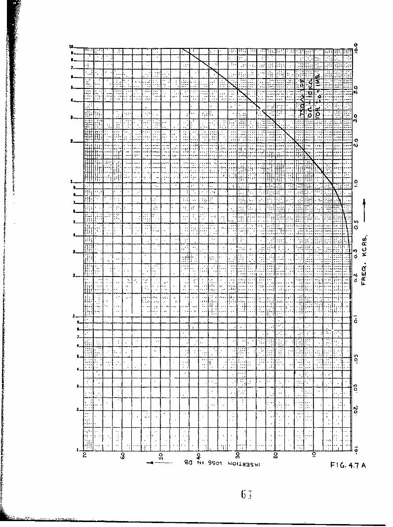
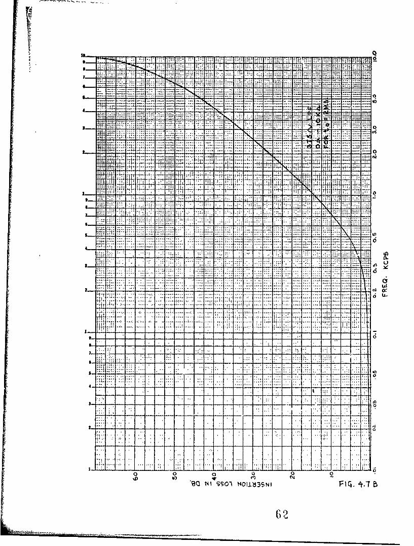
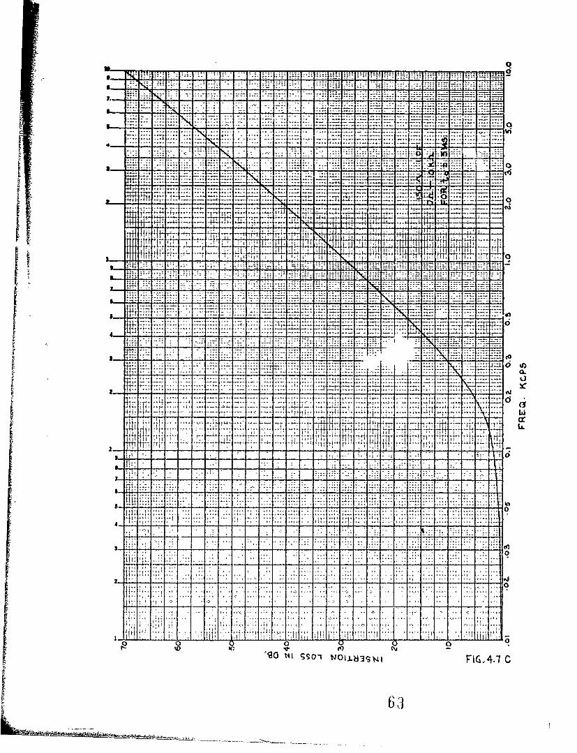
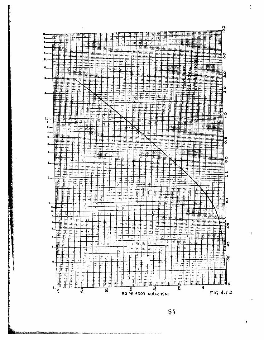
4.3.7 The Low Pass Filter
A simple two element low pass filter was designed for each
pulse length, assuming zero source impedance and a 10 K
load resistance. The filters were designed for the 3 db
4-6
L_3
cutoff shown in Fig. 3.3 and were constructed to have no
over-shoot in their frequency characteiistic. Response
curves for these filters are shown in Fig. 4.7A through
Fig. 4.7F.
The low pass filter and the phase detector are referenced
to +5 volts, established by a bleeder in the decision cir-
cuitry. A pair of emitter followers are used for isolation
and to minimize reference level changes due to the loading
of the decision circuit.
4.3.8 The Decision Circuit
The decision circuit is a voltage comparator circuit de-
signed to give a mark-space or space-mark output change as
the signal from the detector crosses the reference potential
eo (+5 volts). A potentiometer is provided for adjusting the
voltage comparator to provide an output which is neither mark
nor space under no signal conditions. A second control pro-
vides adjustment of a null zone ew from 0 to 70% of the peak-
to-peak signal amplitude centered about eo.
4.4 The Noise Source
A General Radio Random Noise Generator type 1390B was used as a
noise source.• Examination of the output of this generator in a
narrow bandwidth showed amplitude fluctuations of a magnitude that
made setting up for a long test run impossible. Examination of the
characteristics of random noise showed that the envelope of the out-
;-7
ELL
put of a narrow band Gaussian random process contains frequency
components down to very low values and that these components were
causing variations in the RMS voltmeter readings, even though the
unit employed (Flow Corporation Random Signal Voltmeter Model 12Al)
had a time constant of 16 seconds.
It was determined that the output of a low pass filter following
rectified narrow band Gausaian random noise is a function of the
RMS value of input. Therefore, if a bandpass filter ou~put were
rectified and fed through a low pass filter with a time constant of
one second, the resulting output could be used to control the gain
in the noise channal. Variations less than I c/s would be greatly
Sreduced., depending upon the gain in the feedback loop.
This system of feedback control (Fig. 4.9) was used with go.-d
success. The necessary amplifiers were employed in conjunction
with an available bandpass filter to furnish a narrow band AC noise
voltage to a bridge rectifier and low pass filter. A large time
constant (several seconds) was used in the low pass filter and
the resulting DC voltage was used to control the gain of a linear
amplifier.
A commercial bandpass filter (Spencer Kennedy Laboratories Variable
Electronic Filter Model 302) was used to limit the bandwidth of the
noise source. The filtered output was fed through the gain con-
trolled amplifier to the mixer. Reduction in the noise bandwidth
allowed operation at a much higher noise level without clipping
4-8
41'

and eliminated self-resonent responses of the main system filter
at undesired high frequencies. With a noise bandwidth out of the
commercial filter 2.4 kc/s centered about the converter bandpass
mid-frequency and a level of 680 millivolts, the resistive attenu-
ator at the noise feedback bandpass filter was adjusted to give
-1.7 volts bias to the main noise amplifier at, point "X" (S-38).
Under these conditions, changes of -50% and +100% in noise produce
an output change measured after the main system bandpass filter of
less than t4.0%
4.5 Initial Converter Set Up
A single tone signal was fed through the mixer at the approximate
working level of the converter and the waveforms at the output of
the power amplifiers in each channel were examined. Adjustments of
DC operating level were made at point A and point B (Fig. 4.8) so
that the waveform on both channels was symmetrical. These adjust-
ments were effected by means of bleed resistors to the power supply
lines and were made once only, at the beginning of tests. Noise
alone was fed into the system and the output of the low pass filter
was examined on a DC meter with a long time constant. In general,
the reading was not zero, and the resistors in the two halves of
the phase detector were unbalanced slightly to produce a mean read-
ing of zero.
A keyed signal consisting of alternate mark-space tones was applied
which approximated the right amount of shift (Pig. 3.3). The low
pass filter output was examined with the DC meter. The keyed fre-
4-9
quencies were adjusted to give the right amount of shift and
zero output from the low pass filter. Each of the two keyed
frequencies was fed in separately and the gain of the power
amplifiers was adjusted to give a maximum deviation of +5 volts
out of the low pass filter. The converter was then considered
ready for operation at the chosen message rate.
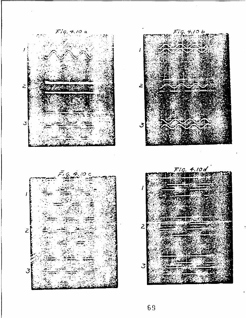
4.6 Converter Waveforms
The operation of the converter is shown in a series of waveform
pictures taken under accual operating conditions at a pulse
length of 20 ms. Center frequency fo for this set of filters
is 1.6 kc/s with mark fl and space f2 t 17.5 c/s of center fre-
quency. A description of the photographs follows:
Fig. 4.10 al Input and output of the first bandpass filter at
F fo with SNR = 20 db.
Fig. 4.10 a2 Input and output of the first bandpass filter at
with SNR = 0db.
Fig. 4.10 a3 Output of limiter #4 at fo with SNR = 0 db and
20 db, respectively. Output amplitude is 1.2
volts peak-to-peak.
Fig. 1.l0 bl Input and output of first bandpass filter at fo
(no amplitude scale preserved).
Fig. 4.10 b2 Input to limiter #1 at fo with ein = 0.5 volts
peak-to-peak and output from limiter #2 with out-
put voltage eo = 1.2 volts peak-to-peak.
Fig. 4.10 b3 Input and output of 900 phase shift integrator at
14-i0
fo (no amplitude scale preserved).
Fig. 4.10 cl Output frou limiter #4 at fo for six SNR conditionsto c3
from top to bottom: No noise, 20 db, 15 db, 10 db,
5 db, and 0 db, respectively.
Fig. 4.10 dl Output waveforms from power amplifiers for fo, fl,to d3
f2, respectively, with eout = 3 volts peak-to-peek.
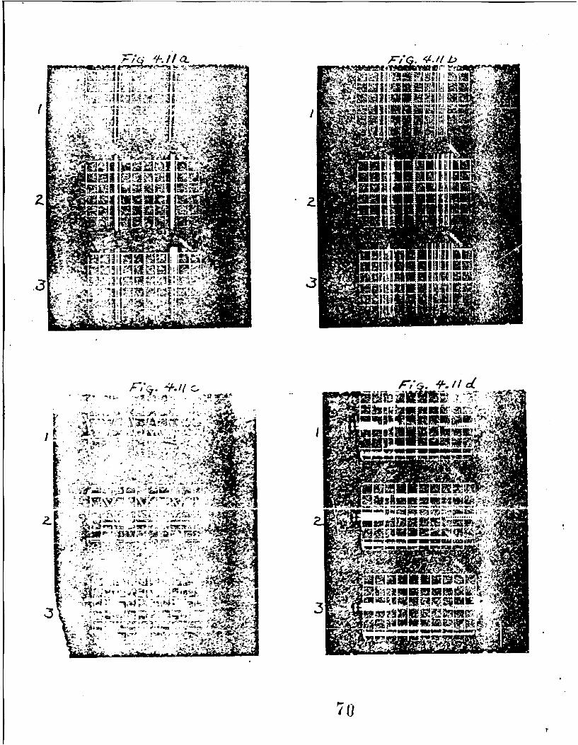
Fig. 4.11 al Output (mark) of decision circuit for No noise, SNRto a3
20 drb, and SNR = 15 db, respectively (leading and
trailing edges of waveform shown only).
Fig. 4.11 bl Output (mark) of decision circuit for SNR = 10 db,to b3
BNR = 5 db, and SNR = 0 db, respectively (leading
and trailing edges of waveform shown only).
Fig. 4.11 cl Output of low pass filter and decision circuit for
mark, mark, space, space, mark, space and 10 volt
amplitude.
Fig. 4.11 c2 Output of phase detector at fo and output of signal
power amplifier.
Fig. 4.11 c3 Phase detector waveforms across diodes DI and D2.
Fig. 4.11 dl Null circuit, decision, and sampling waveforms forto d3
null widths of 50%, 30%, and 10%, respectively.
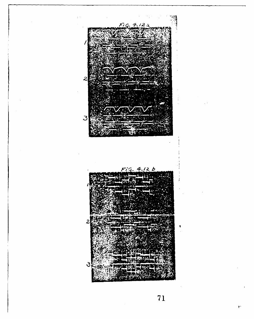
Fig. 4.12 al Integrated output waveform of phase detector vs.to a3%
input 6ignal and reference waveforms for fo, fl, and
f 2 , respectively.
Fig. 4.12 bl Phase detector diode waveforms for fo, fl, and f 2 ,to b3
respectively, where total amplitude is 60 volts
peak-to-peak.
48 4-11
L 48

4--7 Conclusions
This section has presented some of the more important design
considerations and methods used to cope with them. A description
of the overall operation of the converter was given with special
emphasis on the more difficult concepts. Several waveforms were
photographed and appear here to demonstrate operation of the
converter and show the effects of noise. Although design of the
circuits is limited in many respects, proper adjustment of the
system will yield results which are close to the ideal.
The relationship between SNR ratio and pulse edge jitter (for-
tuitous distortion) is shown in a qualitative way in Fig. 4 .11a
and 4.11b.
4-12
[[

FIG. 4.1IA
RRS
RIC. 4.1 a
,' 50
.ý!T,:F MT_F, iE
T= .. .... =3_"
.... . . .. ...
4n-, 7 =_7I. .. .... ....
M. 77 -7 -T: _;T:tFir
Tn"EC7
L-j,717M. ... ..
it, .. . .... ...
NMI--::It---
It nn
771. -41_ ruu
5 im ;_:i! aM
%-ýi! tt
Tit H
00Id
:v- LA.CK
3 t
;:h -1 4i till, Il;4i Hi IHJ :,,-.I
IT
t
Flom n, it H
tt
ýT_titý
1ý4 1in il`q.-M!
it41, 1 ilk -1q,
.7,
IT;
T+ 77ý' t',
t
7
it
0
1;0 N1 ssol t4oub3sw FIG. 4.2 A
.114WT -- K-ALS: vLi S 1111 -4 -1
mum.,
one; in. H i-. 1 1ý- J It- 1 RUE q-
4- A -1 ýýt .4 11.
1 41W H RD i i E Ho how! H .Týff ffM_ .111-:1, iu-, 5.9-1119i ma 1 T.:
....... .......
how twist! + Lr4 Its
4ý N it
44M, I HIT 1111 SOR........... 1. 001 Uý 4+Hl iiiýtt'Kqid of 1 ýD`, + l U 1ýff V al is 1111 W; x it 13 414;
4 N . : :%Wt :
'TU is " 44 MU
i 1K is 14113 1 HU AMIN to 1 S Mt to
11 W 'K A. to I 1111 i q fl -* TK! V. IS I I i1w4ý 9 A : z -
S ol 90IMPRI to 0410" V M 11 Uf 19 P+ It *1211t 49 104 :fq
imMolos +,W t si &R4i I R 9ýh IRM
BERN R 1 A 14 hll*i It M it N 10 NMV! EN IM M M of 0 40 3fi'l Difffiff"100-111 1 T-,, ýjl i RR 1 W-1111 SMýRi iiý 3 4111 v M 11 M RW f sm MR, 14 1
7+q
4 f T, 1 i Do 411 Nuffoo 101 44fWi, k01111 U., owl-11064 oil1 15-111 411 off
. ....... v IT 4 ̀41 Imm W lMl I n ý; In0.
IN 141 Hit! 01 i 1h 114 M VII 1101 +PPRO I !N1 1 suit, i 11-41 oil I l'
"T " ;-ý' 1, 1, 1 P, Q No Dl IS141 i 1off gla, tellMESH 0 Mf 11 wW.4a, flooý.,ý 1 4 liolillofNo 101 HI IS WIN I ifli +1 iWill MR I to P4 a to Mý]] -'-+ N
lot 4 us 12" N Al, 1l`+4"iN11 !14 j N +h 1 IN ff" NO 1 N
tV 11; lun-fN AHS H Mullsw ut +
u'r110" 1 H DI lili H,' i 7 + Oil M d 1 W 1 4 +
I still 4,
111 i 11 1: J 11, 1, i i"I 11111 T 1 BIIto Mi IN! Nii WW$
fill
1 fin, ofilIlhot to
Th, I it pq IR R 11 Ulu to
Itl,+! .411 .4 ip!H,:!: ],i 1 :iýý ;III ý11ý
" I il - 1, Fit T F, 71n I it I I i I 1H Hici viol 1; ..],IH ;..I ; 1;;i ;. i1ii+ +:T, _T " H 'Hojolff; all l7-T WITl:: iNni; NPIPI Ifl;!t Ito
i -IN:
In 11 li,!0 list 9
imp MIR`Eli g lý I HitSIT
...
YH
I i I T' i i'ý' 0 -T
%0 93 01 NQ 11-d 3 9 t4f FIG, +.2. el,
52

E: -- ------- - IL 2--.. . .... .... .... .
FHME: CO. . .... ....
... .... .. 1-.... .... . ..
. .... .........--- - ---- --- ----
... .. .... .... .. ... ...
7Zý
v. t= -11 K HIT
;Hi !IF
i g
+HP-1:1 -4ti- jHi 7:7:
+tl al
-TV
+ N-44':-, . .
ip- -TT E . .. ....Ml ... ...
tllý E Rt ;:.7..
E.
-jj M14 ý&i
-tii HIT. - +
It
+
i -411: ii L-:ýL-j ýInl Ix
'A- 4' -"+it"
1:ii:+ . . - * = .1.4. !1-1: *+:; -*.,;r.-- ttn
I ff UL: "TH:+ 411, 7-- -1::
Hli i, 'V 1ý*Il I.- ... ...-Ti lF, li ji!ý jiE
HilU t" H+ ... ..
;Hi . Tý- ý:: T,
tý- I . -i I ýj.. I . . I . 7.,
I; IP :t:*fr. : +ti+ -t:tj T;";
"17: '-,ýj rjýý
4 iý'.in I:::
tiff ;.- T.+. +W+ !H, :::! ý::: 11
co
.. . ... 'ITL Tj!:
ý: L -..
TT
0
90 W1 SSOI N011bI.SNI F Q. 4. 2- C
Ti H . 4:1 931 iig.. .. ...
ITý =-I ., M, LT.:!:'_ '
M-fl +
t i 'lif
U PW i t Y 7~'40ij; tR 0 [f-t. 40qqj'
0)R N qt j ~i-HFI~~~ ~ ~ a 90tt sT-Hlbw I. .
®r 4t 1-,;I , .C
Hýi co
MAN::
1-; iff i 11-7W: ýýP, 114 i
7ý: +
ah 41 A -
;-t;,
Lj 'm xw-ý il1 i 4 to N T.., 411 A Pot
UR ME-H Al 19 1", ;
R !Hl Toil, ly 02 ga nyiI lit N R
up : MY 10q K NTH it -'a! fi;' - `ýIý !I,-* q1I
till all Iq-
ip post 40 gi,
PP LL
15' 00F U
tit -.H*
.............
t:.. yogi A NN %I T
T. 14ý
Ejj fg4
..........I
l'i iN1 4111 .1::! H, fiH .,- H Ail'IE W, Im mi d*111 Hill [Aw!if !.l:
Rm PUP pot '1141m; it HWJ il i II i:i: 1!H NH a i
+Lt R 1 1 i EH 50!1 T; K 11H m I i: i i P 1 I!t 'I ý U 1, :jii HitRIT
HOto RdEll dd 1
QQ. jN ri T : :1! i
54 Fit
77
I f KID
LL L L; L "IOU
[El-. 44
-4-
.41 +++T -+-t-,-ipg
...... ...... .... tttý ti :M M 0 ITT4441
*# t
+
L 4+4-L44-ý .. .....144H ... tft-Tt
+ 4
r++............ ....
itt
=TITttV+
4444-- 4t-
tit . -1 ý I # 4 :5-ff
+ mm71
t+Lft4 ' 4-
-T
CL
tzi-
4- j
f 4
i-H I
MI
ýT'T14 4
4-
14
4 'RIM m4 t4' ffý IMP'4 f
14
Iti 4 - - ý- 11 1 "I'll, '.14 - rl-ý
W41
+
4++ HH I'll
Rj t+4
ft
4H;
K ý'-tti 'pitI'M4 4 Im I -M "I: V, I
j;;l. !4iT f:1
-1 i;4 11;ý+
RV
4 tJ4
+tT'+1
# 'Ti tH11 :4-i 41,
t4liN Hit i7it
t
14
4 tl
LO ssol Noubsswl F

FIG. 4.3 A
tC R• VouTr
Rg
FIG. 4.3 B
537
AE
WEERENCE
FIG, 4.4 A
EXPECTED TIME UATU'L tMAE
or C.l CMjp~GINC. OF r,3. C4A~RGOAG
FIG. 4.4B
VOLTAGE----S TO AI V~~%oLTAGE ----
VOL'TAGE. - ---
Ca ISCKARGE
VOLTAGE D--- --
DTOCP
VOLTAGE~
VOLTAGE0 TO F
VOL-tAGE F-----------------------
FTOE~OPTIMIZED WA~VrrORMS IAOT
DRAWK TO SC.ALE. F1~ t5

........ ...
.. .... .... ...
..........HH iln 1F_
..... ....... .....ME ;.r-- T=-
...... ......4-t4
7 -il ............... ... ......:=ý:l z
=4_4F;T-- tr:7 :L 41 ý4 t .. . . .... ...
4 _r::4 .. ..............
+r1r
.... .... ....
..... ..... . . ....
444+
w:
........ ........ ........qt 7!9
::7
+
+4+ 444,-
:Iq; :ýP+ 44
++44
4.
itiffIT:
"17
+ .......
4=1 Tý
TztT
fifft 4tTZM
J=:
i 4li t -Tit t
7 4 tI, I -ý ýF_
tt it
tit-+7 7 1 1 9L- , . I ýýý
J'r 74-+4
I+ +
j; 4 4 1 1+ +
+jj.4 I'! Hit I
j r;+
411. .... . Ho
141 1H t i H 14 + t4ý
TT-7
+1ltý tit tt IiL io 14d
.. .... ....
Fl(ý- 4.6
~--- ---- - * -- --- I T *_*.. .... ... ..
.. .. ... ..
I~~~ .... . ...- - ::
N1 1..* .::L 3 M- 4-1 A...
.0
7Z=::7
.. .. . -- --- -, ,17ý
2- " gf
0)
..L... .. ....
.) ...... .
H'T62
----~ ------ ---- -1-
I'~~~~i. "PH--......~--
.. . .... ..... .
co
.................. .0.
C'.r~G ~S~Oi WOI~ 1 F~.44H
6 '
77
- -- - - - - - - - -
V ... .... .......
.. .. . ... ...
--- --- .. ... 1...
7qjyý 'IT, . I ýt - Iff" . ý I ---- 0pffp I I T 14
jrj W it f.1H.1 :4i-..
If 11-t.. .... .... .. _d!2
EP.
;e4=RM41'q !F4-
1t+f f00
i a I I I
T + JT. 7 0
. 1-
lif It + f T1 1111 I'll 11 +4 4+--- 1 *1+1 il
I i t 11 1
'T of
4+
41 CL
Li LitTIT
i if ý4 N.. .... P -1 i .- WIA
t, fl:ii i HIT 1-fl I I I x!7- T7
T-_t 14, -ul44-1 L A 114
r: it-if Mr TF! 1-i
i M-I- ̀ 1_11__.
.. . .... Z;,vtit ftý tý
4;11.4
Ht I 1 1:
I;" i4. iI ' ,
Wit i 1, 1 1;
UI: f71 f
, I; qji
tt Hý 10
0
-rti tý ff 44 1
ý1' Tl 11 1, 1
T T- -T TTTj ij i I t, 11'I,
R ITIN IT
j
it
t1f.
9 C3 'S S 0 N 0 111d:3 9 V41 r I G. 4.1 F_
65
JIF !I, Tru, HiR . 'M
_W1 UlfM. Zia lim
TVT14z.,
Ing
it! ýH
L T,
4 a
4+-W+i f-H4144" 44 ....... ---
Itir tin#14 " " 11 1 H .
IT I 44 11.# fl f t##`44 ..*fH
T T
I I I I T; 1 1I
. . .........
+ ff+ ri 11I + 4+ .1, + +
.M'' li'14 Tfl
T T414 TI All 1'' 1 , fill 11Ti;f
Tr
+. ..........
T TitHiý LA
t': j4 , i 4 Ifl, .41 1f.- 71 &ff E., !,;T 11RM d ý4: 4flIMHill IT, f 4HTP.. .... Mm ý14 -.1, WINEffp U _'i nili UTM ýi4iIfffiH#i iN 444 ..... ..... ..... ..... .....:rz
T
11týl 14'.i4jf ] ý14+ Tt
4*1 11 t it, , . ý:`, , I 1 44
jiliIt 11 1 t N I 1 4 i 11 . I I i
tt 114 '[4' '4
'11, rj, ti4 1
4 r, f r TM ýj ýj If\
Tj- # +
1H1i 5 't tj t
t it i tlll t
94 11 fI pTr4
tr4j414
11
Ti, *11ý110 "'I t 4
t i i . I I I i't t tI t. t 1 ,
TP
t if I ýtlt if
t ;ýilIll' lilt il" i ,4t:
it
it, IT,t ti T
0W1,t4l 9901 NO1,Lb:3SN1 Flfx.or-7 F

KEYER M4
LK % 4X E R - CR 1~ W-
PASSl
LIMIEIZ SHr GRALI$LThk
I~.U)4 CIT~lERTE
L114%TIEIL 'i.8p
DRIVE6 DllVb7
0l
NOISE FEEb\•CK CONT'ROL.
FIG, 4.9
5:
N..
44W
fm"\ ,' V4
ýA_ 4
al i. -Q,
6 93
4& Z w4A~t v ýiio
Av ii ina ra01
Itl
r "ISO,.M
NX ?KlPr~f
71r
Co o
V- cc iT 2 4-tz 0 4
0 - ý t dtL. CC-aI
0U) a) Wg ¶ iý >-~ '0 0 ixO4'0 1 LU <aW
0 t - 3r
UM
Cf)
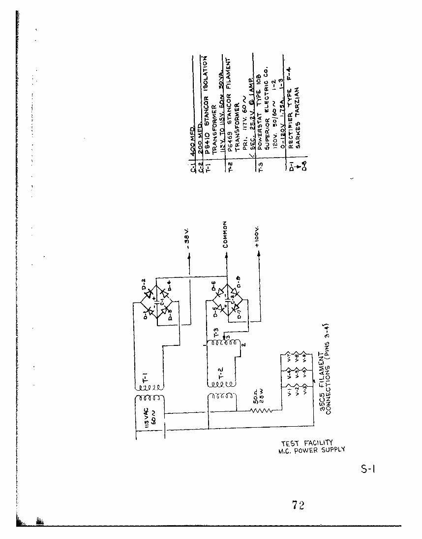
~~to IMA.C, POWER GUPPL'i
S-1
72
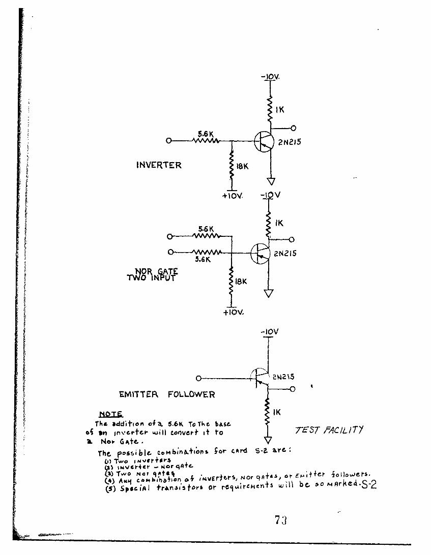
lK
5--
2N2#%f
INVETE~R FOL.WR A/LT
The. addhon oi~5.6K 6Khe ae
4*n $ATet~~o~E,*No..K UTe.
rhc.~osebl. ~~b~n+IclI.or ~rdS-i
(~)Two NV+10V,
- NorV
(4 A~C.Mbf5+O~ ~ rAT~
(5)~ 2V42%5Y~atr o 1 b.~ P.R~e.-
7321
A
III
.002 .002
21 I OV
a +10V IV~ B'
SHIFT REGISTER
7f57 T 4C•iz/7-)
S-3

10
001 +
00
VVVV0
%0 :,%
40'
00 SAS ACLT
Ix-a~t 075
-10
lK 1K
of U~, IN261
a0 1I4Z01 5.6
DIVIDE BY Z
TES-T eqC/L;T1
S-5
76
-10
IKjc
-- C
5.6K|• N.5
16K 18IK •
+10
5.6 K ( , NA•
18K• 18K•
+10
AND TRANSISTOR GATES (TWO)
-S T /--C/-/T 6
5-6
77

INPUT -.02. W.
DMV. AND DRVE
I TEST M:C/L/TXY
S-7

-- --f-
7Iý5 17
4 4
S-8
79
V- I V- 2 V-3
r-t I- T- Z- T-4C'-
10fK 10OK 10K IOK
MC. SODECOIMPULtE COUNTERSTYPE TC~eZ-4-E
25 iMP./Se~C.110V DC,
V- 35C5
Tr TERMioAL- STRIP
+loOV
T- I Ti! T-16 T- Ir T- 18
4V- 5 v6V-7 V-8 V-9
IOK 101K IOK I0K 10 K
-38V. COMMON
TEST FACILITYMECHANICAL COUNTER UNIT
S-9
80
ROMOIL
- 10
Roo 5.6 K -lov curp&T wHwoN1wP c'T Cf4'
5.6K
0--AAW
18 S K'A'Z7
e..',OPARATRsI U
I-1
Ckk
-- ,vvt
-11
'S<
0 144
Lý-TL
7S-1
'41
II
* 7TTs Fct~ 77r
Sd13
-lov
22K IY
.05 tAFD.
oDrFFERENT IATOR
The r.S of+he, circui,*s.LYA sC- )beI-f- ~I4C~nbe- ýOi.& 4 b'j rrýefrrin 1 ot
85~
-. ^.AA V--
Sd
S•DUAL 17 AT F•
77-1`7" .,ýACIW-TY"
rN
S-16
6 7
1kl
S-18

17n___a 1 V
LNI
cii
(S&1

ni
0
ui:
u-01 4
clIl
-TES FACLIT
uSJ-
~9

00)
00
00
0
'0
0 e1-o7Jrx 0
00co3
S-21

eLI-
e' Z _Tor Li- ~c i
(0 z
o 0
o Ao
TEST FACILiTY
S-22
9')
40
LL. CD
00
Liio.4 >-ho LLI
t CO
TEST FACILIETY
S-23
93
0
t~to
cuS ACLT
c-2
In
F!Z
KC04-
z 6i
~0 -
CLt
-AAAAV\V -W/l'VP
0 -
0
~I W
10
TEST FACILITY
S-25

_ °)
F C
S' I~l
I::ca
"T'EST t"CL"(
S-26
(f)

I..
FL
TQ
0 h i
ti
OLITEST rArILITY
57
'4d
0
kii z
0
00I>(00
a-2
S-2
cu >
0.0
0-2
0o 0
ILLAcc
U)
0 CL
oc0
TPJ FACLITY
S-30

II-oo
.L t
0 0"
) II o 0 000
CE co'I
0 c
~o 0 0 0
' - S-I FILiT
-0- edl
-- 31
S!ll].
.3
-0 t, z 0
0 <
~~0
2 0
I " r-• . / •. ,, o _.
•" ,,
0 +J
_ _ _ _ _ _ _ , )- ,= = iD0== • •
~0
-AAJ
+w
00
cu N21m 0,.

t-4
TEST FACILITY
45
," i. I I
• 'I
S-I
.xiij
oZ
'ILu
JEST_ FACILITYS-35

Ii,1
VT
'4.'#
•i, T ST FA ILIT
'4SIS-56
V 'llI,
OD
I 07

44 * 1
00'-0
J - . ** .~ . +.. .. .-
lytO W m .
""4
IL
t- j
• ......
V 0
": &J-13D -A
-. * * * .* ,* . . , 0 L
*
.4. NjO -A j$
4 .S 14 9 .8
QU)
(1) 00
W w :w -J
LI,>- 40 1 J 0
ZO - D F C J ' 0
F C) 2 0 J
W < i a CO & L
<~oc~~
<01?
:Z o-Dz 0 U
ZL'J-i <
0 -0
4ot
L) <
ci <L(0
< 0z l <
0 "9
~~LL)
F- LF-
7I- X 0
F-LlJJ Di 4-YS) 0h-
LL ( C) w oO¾IO
oI CLd Ld D L- L I)C'-lii
CZ)> ,
IF
It
444
IBD-
ININcz01
I
I
o
o 4
o
- D:- AAL~
o re~?U~LJ ~ia L LLŽ.
-I %14.Z) Jr9 Z r-CA N k
I3D-D
11

0 00 00
0 0
0 0 O0
0 00 00
0 00 0
0 00 0,
00F0 00 0 N
r4
'00 0 0O0
0 0o 0 0
0 00 O00
0 O0 0oo
".4 '..
0 00 00
"14
0 00
0 00 00
AG,,/Z ro7P
-X-*Yz
-7 RO.31 4a
Z-4~~~~ 'L W._____- AWT40Ro~ ~L_____S__6_A/__D_____ F
VO. /
AllbAx-
C-7 a' Cg __1____
I3~

, A... ;'
ZSb-5t
ArD.
1/t3
ol /0
0 os-s-
V ~ !I 1'!_Q!i.1I:'ol -1.
Li
I'. 7z ,e2
-3-
7A'
da.7 P.Sr5-14 74. gfP 7 8
~~'Iorw~o 6r. /W rmv GPI'X zl CO/ c~r.
~Pao
n 9r
Cjac7K F14MSE '6ygeAP~oe -
z 130-2
i//a
, T0v-
let~oN9 De *al
.to w 't)
5-3 ie-

V oq dt 4o0
LIA~ ~ ~ 000 7160'
CONI
Ab.97I s-a
Roqj
RedS CF/ Rol^.
C'Q 1-
Sgov* COWg
IK
I14r
-/4/ &F6-/A9be 7R
p RA, -
BD
P~~'64SE AtomI '8
S8D-S 4TS I
WOO-7
OD-"I
D 0 A

c ~ ~ ~ ~ ~ p IShe -- S-5
MY9 -W /0 Rods CA ROIAV
6s3LL
s.oqz
go~6..
-7-2
IIV
Z II 7 -5- FRIa/t/rY38c A Al /PATTliE'N C-veAT6Y9
13D-5
7'8o AW4
446
Apr, by
A7IA
pa~' C-/r 14P3 t4 t -F~OR 1,,4
6-'6
,sP3 AVE~ FO-' 3 X
8-2 ROMQX8 /A. -5 Vi 1. oC-AA kl
ACBD 7SR.41 7SA~O-
F-13i
.441-3Z C#A
IO- SP 2-.Z
26'IosrACECv&AE / 2
r717
OP-OL D-ZvVisAR .YAjf -It
sp ~ q ii- z
~GS _31 SR*01
5-2.
A14?
7- COAI/ rW
03S
f~d..dJ 4~7/ Ij/
fb,6l, S-3 S- O
c O~lp". rdne -- V e ,q#~,fWCo#1mARiSOl
660 -' Stvh-7 8D 5 W-9
c A
Row ROW
xw/ 05. ROeSY Rio,3 A fP01
W-__ __7 SR-r 2. P./
3o, -3 ,r ~ ~ ES"PWTeC6fd'7Roy
6RO "dB-/ D-7
eoll. Car
SHI/FT o'
Ff W 3 , Rw6 R017
D 0
A& I EP z
SR SRI
5f9-.
o~ *bT~
LERROR Rots .9 DR-/t
3Z7
O LT/fER 7T1N AiH 1 7iY Rost 436 o4'(p 45 Roi~ a 2
S-7 3-7 Ob7M4
)-6O
AuR~C~O Lo 44
C-7 4 3x -ri-42-LiP AfCOR-c'1OvDAIS DQ-;'W-
13D-8

R643A.3Xz Cat%' -NRPv
5-,
~'4/A'17 A"'4 rOi'
.r. fat
AO/Al
c~i~?P 'O934R2M
60caw
___ __ __ Z.W4
L41- RON
~ 13 Rav Risk
'Cow'
17K- £1
9 /0 95fl/0
AT 13D-9
- --
A '- C -."P114D- 2EA1V0
0 3Z.-,-?

I-I BIT MC_ PE RRORS
* I
fR RDR$OTH~l
"tHAN PiARITY
W O NUVLLS OR>1 UL.LS Mc-8
RACK L-OCATTION AGr-A
000A iANICAL COUNTERS
TEST FACILIT'YCOUNTER FUINCTIONS
13D

NULLS MESSAG!MC-3 BLOCK,:
NOF PARITYERROR MG-If -.RROR m
IIONE. NULL
FC~ORRCTO CORRECTION~SUCCESSFUL FAILED MC-
DOUBLE OUTLINED BLOCKS REPREGET ME(
WO4 v4 Id O ROMT ROle. AMP. -
A PI o6 O lR041 ROO34TRN
AMP. R4L52 L oIl L ~ bONC.
a30 Sal SalLSa 6 ?.
ROZO4T
11 W E LO-P RC4 Q02 C KT RC'1
R04 4
LIM.-S LIM.-6 DRIVER
;HIT 048 l Amp -2a
;rK KEY(Ft L COWIER-TER ARE.A- 8
13D-1II

I(EYER YKEYF-R toiLt MIXER R4TUNED R041 Roil AMP. 0Ot
C- T 41 Rok3l .1$23 Tr $2.5
Gt4.(u-OR~eB AOLWI
tEXT. I KIF
$3 e Ro07
ROl L14
R04 RO 5
RI

r e T E -, p A '0 e C O u " IT i p R R O L I
MARIC_ __ _ /10
b covivr NRWR
PARITY
~&~X D/4 O'AAWOR
6-erOPA-ZR Ir3D r214C-
S- IT oDC /P-V~r ~leSAC M/1-s 1234
7WN8E77O 6W4Sr,6R I
$81? ~ ~ ~ ~ ~ ~ O COP 'v-' ~rs~ 1
rPAT-rTN G,-teeATO
T T
Related Documents


