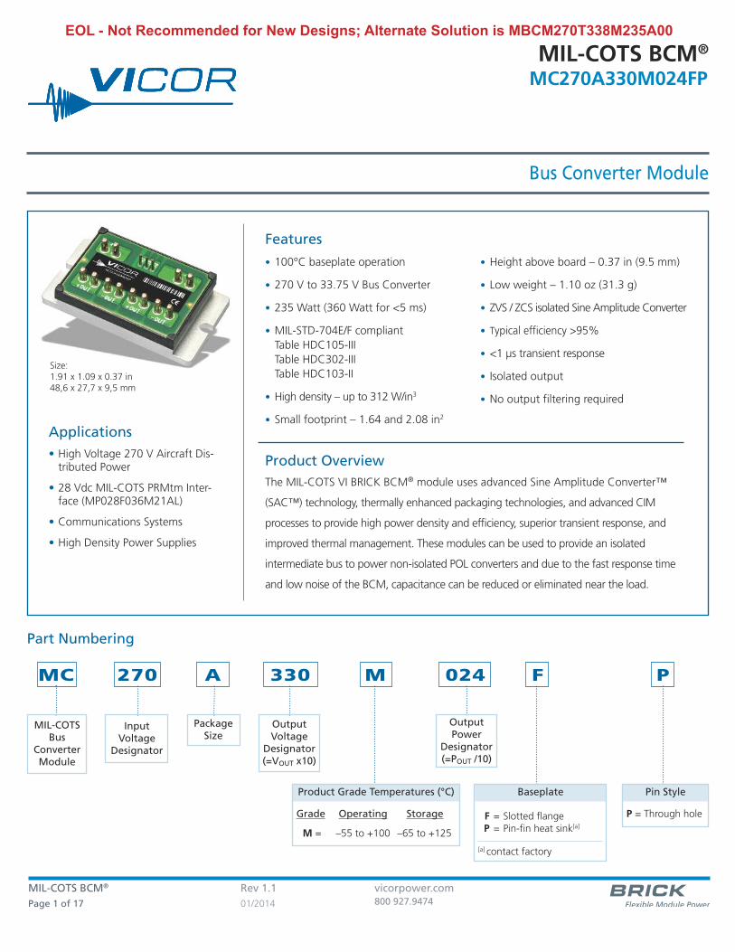
MIL-COTS BCM ® Bus Converter Module MIL-COTS BCM ® Rev 1.1 vicorpower.com Page 1 of 17 01/2014 800 927.9474 EOL - Not Recommended for New Designs; Alternate Solution is MBCM270T338M235A00 MC270A330M024FP Product Grade Temperatures (°C) Grade Operating Storage M = –55 to +100 –65 to +125 Baseplate F = Slotted flange P = Pin-fin heat sink [a] [a] contact factory Product Overview The MIL-COTS VI BRICK BCM ® module uses advanced Sine Amplitude Converter™ (SAC™) technology, thermally enhanced packaging technologies, and advanced CIM processes to provide high power density and efficiency, superior transient response, and improved thermal management. These modules can be used to provide an isolated intermediate bus to power non-isolated POL converters and due to the fast response time and low noise of the BCM, capacitance can be reduced or eliminated near the load. Applications • High Voltage 270 V Aircraft Dis- tributed Power • 28 Vdc MIL-COTS PRMtm Inter- face (MP028F036M21AL) • Communications Systems • High Density Power Supplies • 100°C baseplate operation • 270 V to 33.75 V Bus Converter • 235 Watt (360 Watt for <5 ms) • MIL-STD-704E/F compliant Table HDC105-III Table HDC302-III Table HDC103-II • High density – up to 312 W/in 3 • Small footprint – 1.64 and 2.08 in 2 • Height above board – 0.37 in (9.5 mm) • Low weight – 1.10 oz (31.3 g) • ZVS / ZCS isolated Sine Amplitude Converter • Typical efficiency >95% • <1 μs transient response • Isolated output • No output filtering required Features MC 270 A 330 M 024 F P Output Voltage Designator (=V OUT x10) Output Power Designator (=P OUT /10) Part Numbering MIL-COTS Bus Converter Module Input Voltage Designator Package Size Pin Style P = Through hole Size: 1.91 x 1.09 x 0.37 in 48,6 x 27,7 x 9,5 mm

Welcome message from author
This document is posted to help you gain knowledge. Please leave a comment to let me know what you think about it! Share it to your friends and learn new things together.
Transcript
MIL-COTS BCM®
Bus Converter Module
MIL-COTS BCM® Rev 1.1 vicorpower.comPage 1 of 17 01/2014 800 927.9474
EOL - Not Recommended for New Designs; Alternate Solution is MBCM270T338M235A00
MC 270 A 330 M0 24 FP
Product Grade Temperatures (°C)
Grade Operating Storage
M = –55 to +100 –65 to +125
Baseplate
F = Slotted flangeP = Pin-fin heat sink[a]
[a] contact factory
Product OverviewThe MIL-COTS VI BRICK BCM® module uses advanced Sine Amplitude Converter™
(SAC™) technology, thermally enhanced packaging technologies, and advanced CIM
processes to provide high power density and efficiency, superior transient response, and
improved thermal management. These modules can be used to provide an isolated
intermediate bus to power non-isolated POL converters and due to the fast response time
and low noise of the BCM, capacitance can be reduced or eliminated near the load.
Applications• High Voltage 270 V Aircraft Dis-
tributed Power
• 28 Vdc MIL-COTS PRMtm Inter-face (MP028F036M21AL)
• Communications Systems
• High Density Power Supplies
• 100°C baseplate operation
• 270 V to 33.75 V Bus Converter
• 235 Watt (360 Watt for <5 ms)
• MIL-STD-704E/F compliantTable HDC105-IIITable HDC302-IIITable HDC103-II
• High density – up to 312 W/in3
• Small footprint – 1.64 and 2.08 in2
• Height above board – 0.37 in (9.5 mm)
• Low weight – 1.10 oz (31.3 g)
• ZVS / ZCS isolated Sine Amplitude Converter
• Typical efficiency > 95 %
• <1 µs transient response
• Isolated output
• No output filtering required
Features
MC 270 A 330 M 0 24 F P
OutputVoltage
Designator(=VOUT x10)
OutputPower
Designator(=POUT /10)
Part Numbering
MIL-COTSBus
ConverterModule
InputVoltage
Designator
PackageSize
Pin Style
P = Through hole
Size:1.91 x 1.09 x 0.37 in48,6 x 27,7 x 9,5 mm

EOL - Not Recommended for New Designs; Alternate Solution is MBCM270T338M235A00
MIL-COTS BCM® Rev 1.1 vicorpower.comPage 2 of 17 01/2014 800 927.9474
MC 270 A 330 M0 24 FP
CONTROL PIN SPECIFICATIONSSee page 13 for further application details and guidelines.
PC – VI BRICK® BCM® Primary Control
The PC pin can enable and disable the BCM. When held below VPC_DIS the
BCM shall be disabled. When allowed to float with an impedance to –IN of
greater than 50 kΩ the module will start. When connected to another BCM
PC pin, the BCMs will start simultaneously when enabled. The PC pin is
capable of being driven high by either an external logic signal or internal
pull up to 5 V (operating).
TM – VI BRICK® BCM® Temperature Monitor
The TM pin monitors the internal temperature of the BCM within an
accuracy of +5/-5°C. It has a room temperature setpoint of ~3.0 V and an
approximate gain of 10 mV/°C. It can source up to 100 µA and may also be
used as a “Power Good” flag to verify that the BCM is operating.
Note: If TM is not used to validate the thermal management
system, a 100°C case (baseplate) maximum applies.
SPECIFICATIONS
Absolute Maximum RatingsMin Max Unit
+In to –In -1.0 + 400 Vdc
PC to –In -0.3 + 20 Vdc
TM to –In -0.3 + 7 Vdc
+In /-In to +Out /-Out (hipot) 4242 V
+In /-In to +Out /-Out (working) 500 V
+Out to –Out -1.0 + 60 Vdc

EOL - Not Recommended for New Designs; Alternate Solution is MBCM270T338M235A00
MIL-COTS BCM® Rev 1.1 vicorpower.comPage 3 of 17 01/2014 800 927.9474
MC 270 A 330 M0 24 FP
Attribute Symbol Conditions / Notes Min Typ Max UnitVoltage Range VIN 240 270 330 Vdc
dV/dt dVIN /dt 1 V/µs
Quiescent Power PQ PC connected to -IN 395 410 mW
No Load Power Dissipation PNL VIN = 240 to 330 V 10 W
Inrush Current Peak IINR_PVIN = 330 V COUT = 100 µF, 2.5 4
APOUT = 235 W
DC Input Current IIN_DC POUT = 235 W 0.95 A
K Factor ( VOUT ) K 1/ 8 VIN
Output Power (Average) POUTVIN = 270 VDC; See Figure 14 235
WVIN = 240 – 330 VDC; See Figure 14 215
Output Power (Peak) POUT_PVIN = 270 VDC 352.5 WAverage POUT < = 235 W, Tpeak < 5 ms
Output Voltage VOUT See Page 11; No load 30 41.25 V
Output Current (Average) IOUT Pout < = 235 W 7.3 A
Efficiency (Ambient) h�VIN = 270 V, POUT = 235 W 94.1 95.4
%VIN = 240 V to 330 V, POUT = 235 W 94 95.2
Efficiency (Hot) h� VIN = 270 V, TJ = 100 ° C,POUT = 235 W 93.7 94.7 %
Minimum Efficiency h� 60 W < POUT < 235 W Max 90 %
(Over Load Range)
Output Resistance (Ambient) ROUT TJ = 25 ° C 100 130 170 mΩOutput Resistance (Hot) ROUT TJ = 125 ° C 130 180 210 mΩOutput Resistance (Cold) ROUT TJ = -55 ° C 40 105 160 mΩLoad Capacitance COUT 100 uF
Switching Frequency FSW 1.56 1.64 1.72 MHz
Ripple Frequency FSW_RP 3.12 3.28 3.44 MHz
Output Voltage Ripple VOUT_PPCOUT = 0 µF, POUT = 235 W, VIN = 270 V,
160 400 mV See Page 15
VIN to VOUT (Application of VIN) TON1 VIN = 270 V, CPC = 0; See Figure 17 460 540 620 ms
PCPC Voltage (Operating) VPC 4.7 5 5.3 V
PC Voltage (Enable) VPC_EN 2 2.5 3 V
PC Voltage (Disable) VPC_DIS 1.95 V
PC Source Current (Startup) IPC_EN 50 100 300 uA
PC Source Current (Operating) IPC_OP 2 3.5 5 mA
PC Internal Resistance RPC_SNK Internal pull down resistor 50 150 400 kΩPC Capacitance (Internal) CPC_INT See Page 13 1000 pF
PC Capacitance (External) CPC_EXT External capacitance delays PC enable time 1000 pF
External PC Resistance RPC Connected to –VIN 50 kΩPC External Toggle Rate FPC_TOG 1 Hz
PC to VOUT with PC Released Ton2VIN = 270 V, Pre-applied
50 100 150 µsCPC = 0, COUT = 0; See Figure 17
PC to VOUT, Disable PC TPC_DISVIN = 270 V, Pre-applied
4 10 µsCPC = 0, COUT = 0; See Figure 17
Specifications apply over all line and load conditions unless otherwise noted; Boldface specifications apply over the temperature range of -55 °C < TC < 100°C (T-Grade); All other specifications are at TC = 25 ºC unless otherwise noted
SPECIFICATIONS (CONT.)
Electrical Characteristics
EOL - Not Recommended for New Designs; Alternate Solution is MBCM270T338M235A00
MIL-COTS BCM® Rev 1.1 vicorpower.comPage 4 of 17 01/2014 800 927.9474
MC 270 A 330 M0 24 FP
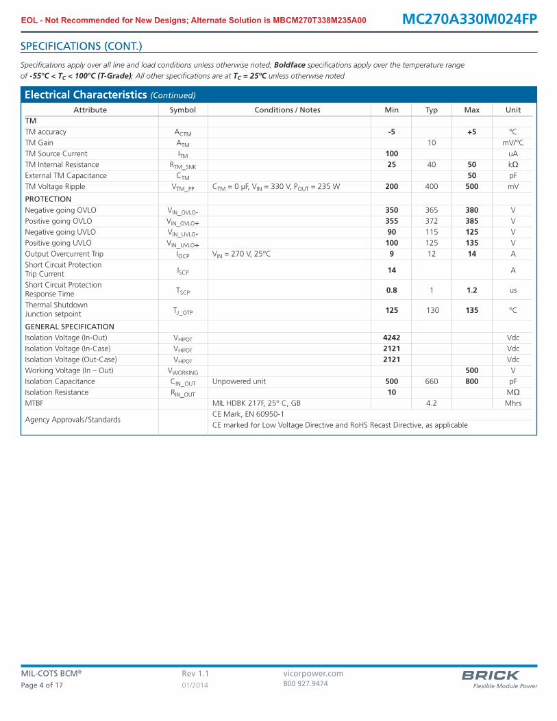
Specifications apply over all line and load conditions unless otherwise noted; Boldface specifications apply over the temperature range of -55 °C < TC < 100°C (T-Grade); All other specifications are at TC = 25 ºC unless otherwise noted
Attribute Symbol Conditions / Notes Min Typ Max UnitTMTM accuracy ACTM -5 + 5 ºC
TM Gain ATM 10 mV/°C
TM Source Current ITM 100 uA
TM Internal Resistance RTM_SNK 25 40 50 kΩExternal TM Capacitance CTM 50 pF
TM Voltage Ripple VTM_PP CTM = 0 µF, VIN = 330 V, POUT = 235 W 200 400 500 mV
PROTECTIONNegative going OVLO VIN_OVLO- 350 365 380 V
Positive going OVLO VIN_OVLO+ 355 372 385 V
Negative going UVLO VIN_UVLO- 90 115 125 V
Positive going UVLO VIN_UVLO+ 100 125 135 V
Output Overcurrent Trip IOCP VIN = 270 V, 25°C 9 12 14 A
Short Circuit Protection ISCP
14 ATrip Current
Short Circuit ProtectionTSCP
0.8 1 1.2 usResponse Time
Thermal Shutdown TJ_OTP
125 130 135 °CJunction setpoint
GENERAL SPECIFICATIONIsolation Voltage (In-Out) VHIPOT 4242 Vdc
Isolation Voltage (In-Case) VHIPOT 2121 Vdc
Isolation Voltage (Out-Case) VHIPOT 2121 Vdc
Working Voltage (In – Out) VWORKING 500 V
Isolation Capacitance CIN_OUT Unpowered unit 500 660 800 pF
Isolation Resistance RIN_OUT 10 MΩMTBF MIL HDBK 217F, 25° C, GB 4.2 Mhrs
Agency Approvals /StandardsCE Mark, EN 60950-1
CE marked for Low Voltage Directive and RoHS Recast Directive, as applicable
Electrical Characteristics (Continued)
SPECIFICATIONS (CONT.)

EOL - Not Recommended for New Designs; Alternate Solution is MBCM270T338M235A00
MIL-COTS BCM® Rev 1.1 vicorpower.comPage 5 of 17 01/2014 800 927.9474
MC 270 A 330 M0 24 FP
Attribute Symbol Conditions / Notes Typ UnitNo Load Power PNL VIN = 270 V, PC enabled; See Figure 1 5.5 W
Inrush Current Peak INR_P COUT = 100 µF, POUT = 235 W 2.5 A
Efficiency (Ambient) η VIN = 270 V, POUT = 235 W 95.4 %
Efficiency (Hot – 100°C) η VIN = 270 V, POUT = 235 W 94.7 %
Output Resistance (-40°C) ROUT VIN = 270 V 105 mΩOutput Resistance (25°C) ROUT VIN = 270 V 130 mΩOutput Resistance (120°C) ROUT VIN = 270 V 180 mΩOutput Voltage Ripple VOUT_PP
COUT = 0 uF, POUT = 235 W @ VIN = 270 , 160 mV
VIN = 270 V
VOUT Transient (Positive) VOUT_TRAN+IOUT_STEP = 0 TO 7.3 A,
1.4 VISLEW >10 A/us; See Figure 11
VOUT Transient (Negative) VOUT_TRAN-IOUT_STEP = 7.3 A to 0 A,
1.3 VISLEW > 10 A/us; See Figure 12
Undervoltage LockoutTUVLO 150 usResponse Time
Output Overcurrent Response Time TOCP 9 < IOCP < 14 A 5 ms
Overvoltage Lockout Response Time TOVLO 120 µs
TM Voltage (Ambient) VTM_AMB TJ @ 27°C 3 V
All specifications are at TC = 25 ºC unless otherwise noted. See associated figures for general trend data.
SPECIFICATIONS (CONT.)
Application Characteristics

EOL - Not Recommended for New Designs; Alternate Solution is MBCM270T338M235A00
MIL-COTS BCM® Rev 1.1 vicorpower.comPage 6 of 17 01/2014 800 927.9474
MC 270 A 330 M0 24 FP
0123456789
230 250 270 290 310 330
No Load Power Dissipation vs Line
Input Voltage (V)
No L
oad
Powe
r Diss
ipat
ion
(W)
-55°C 25°C 100°CT :CASE
94.294.494.694.895.095.295.495.695.896.0
-100 -50 0 50 100 150Case Temperature (C)
Effic
ienc
y (%
)
Full Load Efficiency vs. Case Temperature
240 V 270 V 330 VV :IN
65
70
75
80
85
90
95
0 1 2 3 4 5 6 7 85
7
9
11
13
15
Efficiency & Power Dissipation -55°C Case
Output Current (A)
Eff
icie
ncy
(%
)
Po
wer
Dis
sip
atio
n (
W)
240 V 270 V 330 VV :IN 240 V 270 V 330 V
η
PD
80828486889092949698
0 1 2 3 4 5 6 7 83
5
7
9
11
13
15
Efficiency & Power Dissipation vs. 25°C Case
Output Current (A)
Effic
iency
(%)
Powe
r Diss
ipat
ion
(W)
240 V 270 V 330 VV :IN 240 V 270 V 330 V
η
PD
80828486889092949698
0 1 2 3 4 5 6 7 82.5
4.5
6.5
8.5
10.5
12.5
14.5
16.5
Efficiency & Power Disspiation 100°C Case
Output Current (A)
Effic
iency
(%)
240 V 270 V 330 VV :IN 240 V 270 V 330 V
Powe
r Diss
ipat
ion
(W)η
PD
90
100
110
120
130
140
150
160
170
180
190
-80 -60 -40 -20 0 20 40 60 80 100 120
ROUT vs. Case Temperature
Case Temperature (°C)
ÊRou
t (m
Ω)
I :OUT 0.73 A 7.3 A
Figure 1 — No load power dissipation vs. VIN; TCASE Figure 2 — Full load efficiency vs. temperature; VIN
Figure 3 — Efficiency and power dissipation at -55 °C (case); VIN Figure 4 — Efficiency and power dissipation at 25 °C (case); VIN
Figure 5 — Efficiency and power dissipation at 100 °C (case); VIN Figure 6 — ROUT vs. temperature vs. IOUT
SPECIFICATIONS (CONT.)
WAVEFORMS
EOL - Not Recommended for New Designs; Alternate Solution is MBCM270T338M235A00
MIL-COTS BCM® Rev 1.1 vicorpower.comPage 7 of 17 01/2014 800 927.9474
MC 270 A 330 M0 24 FP
0
20
40
60
80
100
120
140
160
180
0 1 2 3 4 5 6 7 8
Ripple vs. Load
Load Current (A)
Ripp
le (m
V pk
-pk)
Vpk-pk (mV)
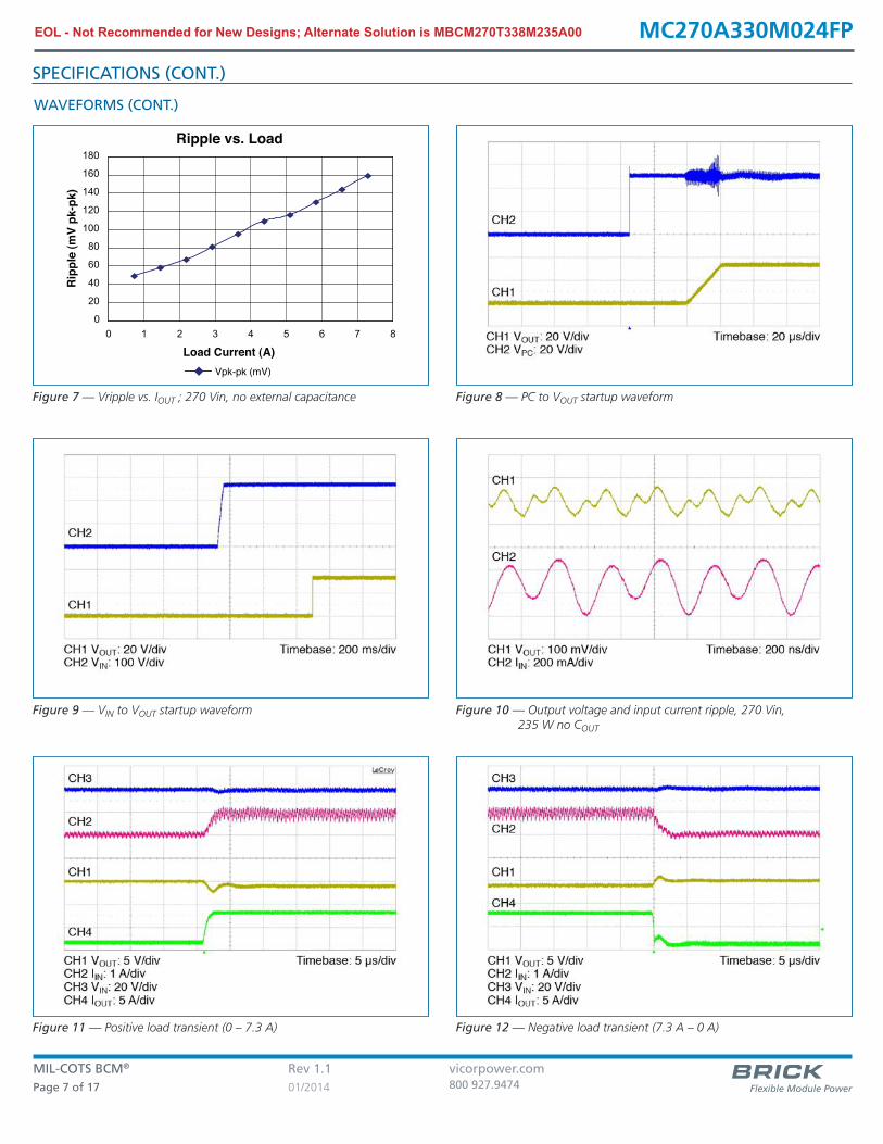
Figure 7 — Vripple vs. IOUT ; 270 Vin, no external capacitance Figure 8 — PC to VOUT startup waveform
Figure 9 — VIN to VOUT startup waveform Figure 10 — Output voltage and input current ripple, 270 Vin, 235 W no COUT
Figure 11 — Positive load transient (0 – 7.3 A) Figure 12 — Negative load transient ( 7.3 A – 0 A)
SPECIFICATIONS (CONT.)
WAVEFORMS (CONT.)

EOL - Not Recommended for New Designs; Alternate Solution is MBCM270T338M235A00
MIL-COTS BCM® Rev 1.1 vicorpower.comPage 8 of 17 01/2014 800 927.9474
MC 270 A 330 M0 24 FP
Figure 13 — PC disable waveform, 270 VIN, 100 µF COUT full load
0
50
100
150
200
250
300
350
400
29.00 31.00 33.00 35.00 37.00 39.00 41.00
Out
put P
ower
(W)
Steady State 5 mS 352.5 W Ave
Safe Operating Area
Figure 14 — Safe Operating Area vs. VOUT
0 20 40 60 80 100 120
125
150
200
250
280
300
330
350
400
OVP
Normal Operating Range
50 mS operationfull current
MIL-STD-704F Envelope of normal V transients for 270 Vdc systems
50 mS full current 1% duty 50% rated current
V DC
mS
UVL
Figure 15 — Envelope of normal voltage transient for 270 volts DC system.
SPECIFICATIONS (CONT.)
WAVEFORMS (CONT.)
EOL - Not Recommended for New Designs; Alternate Solution is MBCM270T338M235A00
MIL-COTS BCM® Rev 1.1 vicorpower.comPage 9 of 17 01/2014 800 927.9474
MC 270 A 330 M0 24 FP
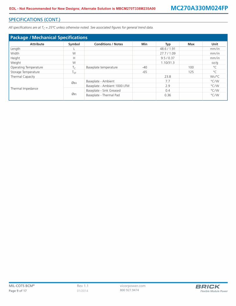
Attribute Symbol Conditions / Notes Min Typ Max UnitLength L 48.6 / 1.91 mm/in
Width W 27.7 / 1.09 mm/in
Height H 9.5 / 0.37 mm/in
Weight W 1.10/31.3 oz/g
Operating Temperature TC Baseplate temperature -40 100 °C
Storage Temperature TST -65 125 °C
Thermal Capacity 23.8 Ws /°C
Thermal Impedance
ØBABaseplate - Ambient 7.7 °C/ W
Baseplate - Ambient 1000 LFM 2.9 °C/ W
ØBS
Baseplate - Sink Greased 0.4 °C/ W
Baseplate - Thermal Pad 0.36 °C/ W
All specifications are at TC = 25 ºC unless otherwise noted. See associated figures for general trend data.
SPECIFICATIONS (CONT.)
Package /Mechanical Specifications
EOL - Not Recommended for New Designs; Alternate Solution is MBCM270T338M235A00
MIL-COTS BCM® Rev 1.1 vicorpower.comPage 10 of 17 01/2014 800 927.9474
MC 270 A 330 M0 24 FP
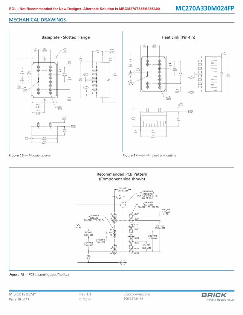
Figure 16 — Module outline Figure 17 — Pin-fin heat sink outline
Figure 18 — PCB mounting specifications
Recommended PCB Pattern
(Component side shown)
Baseplate - Slotted Flange Heat Sink (Pin-fin)
MECHANICAL DRAWINGS
EOL - Not Recommended for New Designs; Alternate Solution is MBCM270T338M235A00
MIL-COTS BCM® Rev 1.1 vicorpower.comPage 11 of 17 01/2014 800 927.9474
MC 270 A 330 M0 24 FP
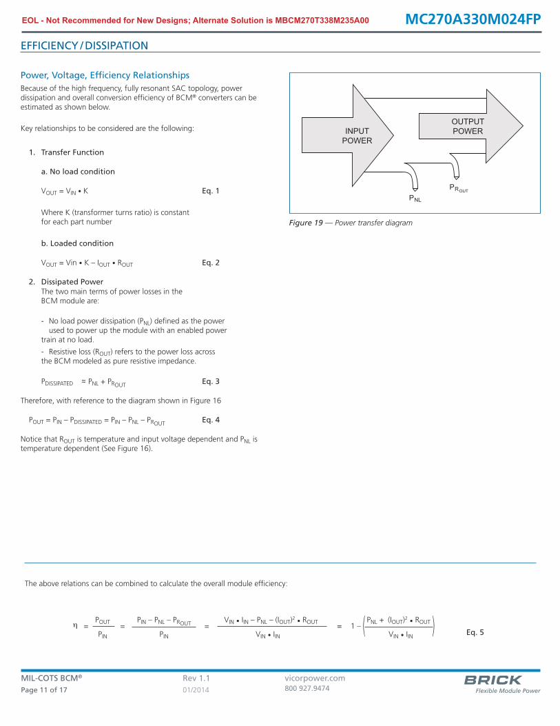
Power, Voltage, Efficiency RelationshipsBecause of the high frequency, fully resonant SAC topology, power dissipation and overall conversion efficiency of BCM® converters can be estimated as shown below.
Key relationships to be considered are the following:
1. Transfer Function
a. No load condition
VOUT = VIN • K Eq. 1
Where K (transformer turns ratio) is constant for each part number
b. Loaded condition
VOUT = Vin • K – IOUT • ROUT Eq. 2
2. Dissipated PowerThe two main terms of power losses in the BCM module are:
- No load power dissipation (PNL) defined as the power used to power up the module with an enabled power
train at no load.
- Resistive loss (ROUT) refers to the power loss across the BCM modeled as pure resistive impedance.
PDISSIPATED ~ PNL + PROUT Eq. 3~
Therefore, with reference to the diagram shown in Figure 16
POUT = PIN – PDISSIPATED = PIN – PNL – PROUT Eq. 4
Notice that ROUT is temperature and input voltage dependent and PNL istemperature dependent (See Figure 16).
INPUTPOWER
OUTPUTPOWER
PNL
PROUT
Figure 19 — Power transfer diagram
The above relations can be combined to calculate the overall module efficiency:
h =POUT
=PIN – PNL – PROUT =
PIN PIN
VIN • IIN – PNL – (IOUT)2 • ROUT= 1 – ( PNL + (IOUT)2 • ROUT )VIN • IIN VIN • IIN Eq. 5
EFFICIENCY /DISSIPATION
EOL - Not Recommended for New Designs; Alternate Solution is MBCM270T338M235A00
MIL-COTS BCM® Rev 1.1 vicorpower.comPage 12 of 17 01/2014 800 927.9474
MC 270 A 330 M0 24 FP
12
34
56
V UVL
O+
PC 5 V
3 V
LL •
K
A: T
ON
1B:
TO
VLO
*C:
Max
reco
very
tim
eD
:TU
VLO
E: T
ON
2F:
TO
CPG
: TPC
–DIS
H: T
SSP*
*
1: C
ontr
olle
r sta
rt2:
Con
trol
ler t
urn
o!3:
PC
rele
ase
4: P
C pu
lled
low
5: P
C re
leas
ed o
n ou
tput
SC
6: S
C re
mov
ed
Vout TM
3 V
@ 2
7°C
0.4
V
V IN 3
V5
V2.
5 V
500m
Sbe
fore
retr
ial
V UVL
O–
A
B
E
H
I SSP
I OU
T
I OCP
G
F
D
C
V OVL
O+
V O
VLO
–
V OVL
O+
NL
Not
es:
– T
imin
g an
d vo
ltage
is n
ot to
sca
le
–
Err
or p
ulse
wid
th is
load
dep
ende
nt
*M
in v
alue
sw
itchi
ng o
!**
From
det
ectio
n of
err
or to
pow
er tr
ain
shut
dow
n
C
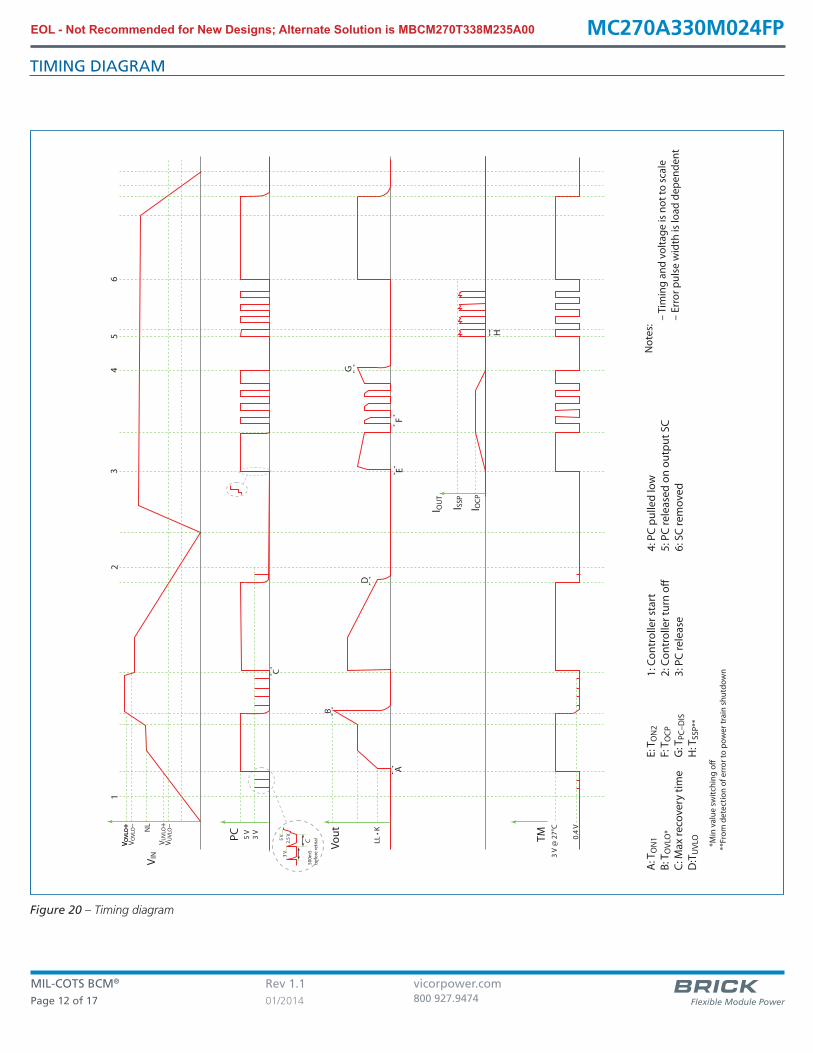
Figure 20 – Timing diagram
TIMING DIAGRAM
EOL - Not Recommended for New Designs; Alternate Solution is MBCM270T338M235A00
MIL-COTS BCM® Rev 1.1 vicorpower.comPage 13 of 17 01/2014 800 927.9474
MC 270 A 330 M0 24 FP
Using the Control Signals TM and PCThe PC control pin can be used to accomplish the following functions:
• Delayed start: At start-up, PC pin will source a constant 100 uA current to the internal RC network. Adding an external capacitor will allow further delay in reaching the 2.5 V threshold for module start.
• Synchronized start up: In a parallel module array, PC pins shall be connected in order to ensure synchronous start of all the units. While every controller has a calibrated 2.5 V reference on PC comparator, many factors might cause different timing in turning on the 100 uA current source on each module, i.e.:
– Different VIN slew rate
– Statistical component value distributionBy connecting all PC pins, the charging transient will be shared and all the modules will be enabled synchronously.
• Auxiliary voltage source: Once enabled in regular operational conditions (no fault), each BCM® PC provides a regulated 5 V, 2 mA voltage source.
• Output Disable: PC pin can be actively pulled down in order to disable module operations. Pull down impedance shall be lower than 850 Ω and toggle rate lower than 1 Hz.
• Fault detection flag: The PC 5 V voltage source is internally turned off as soon as a fault is detected. After a minimum disable time, the module tries to re-start, and PC voltage is re-enabled. For system monitoring purposes (microcontroller interface) faults are detected on falling edges of PC signal.
It is important to notice that PC doesn’t have current sink capability (only 150 kΩ typical pull down is present), therefore, in an array, PC line will not be capable of disabling all the modules if a fault occurs on one of them.
The temperature monitor (TM) pin provides a voltage proportional to theabsolute temperature of the converter control IC.
It can be used to accomplish the following functions:
• Monitor the control IC temperature: The temperature in Kelvin is equal to the voltage on the TM pin scaled by x100. (i.e. 3.0 V = 300 K = 27ºC). It is important to remember that VI BRICKs are multi-chip modules, whose temperature distribution greatly vary for each part number as well with input/output conditions, thermal management and environmental conditions. Therefore, TM cannot be used to thermally protect the system.
• Fault detection flag: The TM voltage source is internally turned off as soon as a fault is detected. After a minimum disable time, the module tries to re-start, and TM voltage is re-enabled.
Fuse Selection
VI BRICK®s are not internally fused in order to provide flexibility in configur-ing power systems. Input line fusing of VI BRICKs is recommended at sys-tem level, in order to provide thermal protection in case of catastrophic failure.
The fuse shall be selected by closely matching system requirements with the following characteristics:
• Current rating (usually greater than maximum BCM current)
• Maximum voltage rating (usually greater than the maximum possible input voltage)
• Ambient temperature
• Nominal melting I2t• Recommended fuse: ≤2.5 A Bussmann PC-Tron or
SOC type 36CFA.
CONTROL FUNCTIONS / FUSING
EOL - Not Recommended for New Designs; Alternate Solution is MBCM270T338M235A00
MIL-COTS BCM® Rev 1.1 vicorpower.comPage 14 of 17 01/2014 800 927.9474
MC 270 A 330 M0 24 FP
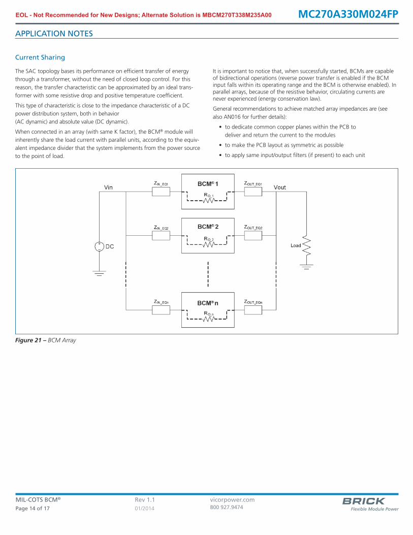
Current Sharing
The SAC topology bases its performance on efficient transfer of energy
through a transformer, without the need of closed loop control. For this
reason, the transfer characteristic can be approximated by an ideal trans-
former with some resistive drop and positive temperature coefficient.
This type of characteristic is close to the impedance characteristic of a DC
power distribution system, both in behavior
(AC dynamic) and absolute value (DC dynamic).
When connected in an array (with same K factor), the BCM® module will
inherently share the load current with parallel units, according to the equiv-
alent impedance divider that the system implements from the power source
to the point of load.
It is important to notice that, when successfully started, BCMs are capableof bidirectional operations (reverse power transfer is enabled if the BCMinput falls within its operating range and the BCM is otherwise enabled). Inparallel arrays, because of the resistive behavior, circulating currents arenever experienced (energy conservation law).
General recommendations to achieve matched array impedances are (see
also AN016 for further details):
• to dedicate common copper planes within the PCB to
deliver and return the current to the modules
• to make the PCB layout as symmetric as possible
• to apply same input/output filters (if present) to each unit
Figure 21 – BCM Array
APPLICATION NOTES
EOL - Not Recommended for New Designs; Alternate Solution is MBCM270T338M235A00
MIL-COTS BCM® Rev 1.1 vicorpower.comPage 15 of 17 01/2014 800 927.9474
MC 270 A 330 M0 24 FP
Input and Output Filter Design
A major advantage of SAC systems versus conventional PWM converters isthat the transformers do not require large functional filters. The resonantLC tank, operated at extreme high frequency, is amplitude modulated as afunction of input voltage and output current, and efficiently transferscharge through the isolation transformer. A small amount of capacitance,embedded in the input and output stages of the module, is sufficient forfull functionality and is key to achieve power density.
This paradigm shift requires system design to carefully evaluate external fil-ters in order to:
1. Guarantee low source impedance:
To take full advantage of the BCM® dynamic response, the impedance presented to its input terminals must be low from DC to approximately 5 MHz. The connection of the VI BRICK to its power source should be implemented with minimal distribution inductance. If the interconnect inductance exceeds 100 nH, the input should be bypassed with a RC damper to retain low source impedance and stable operation. With an interconnect inductance of 200 nH, the RC damper may be as high as 1 µF in series with 0.3 Ω. A single electrolytic or equivalent low-Q capacitor may be used in place of the series RC bypass.
2. Further reduce input and/or output voltage ripple without sacrificing dynamic response:
Given the wide bandwidth of the BCM, the source response is generally the limiting factor in the overall system response. Anomalies in the response of the source will appear at the output of the BCM multiplied by its K factor. This is illustrated in Figures 11 and 12.
3. Protect the module from overvoltage transients imposed by the system that would exceed maximum ratings and cause failures:
The VI BRICK input/output voltage ranges shall not be exceeded. An internal overvoltage lockout function prevents operation outside of the normal operating input range. Even during this condition, the powertrain is exposed to the applied voltage and power MOSFETs must withstand it. A criterion for protection is the maximum amount of energy that the input or output switches can tolerate if avalanched.
Total load capacitance at the output of the BCM shall not exceed the speci-fied maximum. Owing to the wide bandwidth and low output impedance of the BCM, low frequency bypass capacitance and significantenergy storage may be more densely and efficiently provided by adding ca-pacitance at the input of the BCM. At frequencies <500 kHz the BCM ap-pears as an impedance of ROUT between the source and load. Within this frequency range capacitance at the input appears as effectivecapacitance on the output per the relationship defined in Eq. 5.
COUT =CIN Eq. 6K2
This enables a reduction in the size and number of capacitors used in a typi-
cal system.
APPLICATION NOTES (CONT.)

EOL - Not Recommended for New Designs; Alternate Solution is MBCM270T338M235A00
MIL-COTS BCM® Rev 1.1 vicorpower.comPage 16 of 17 01/2014 800 927.9474
MC 270 A 330 M0 24 FP
+Vout
-Vout
Mod
ulat
or
+Vin
PC
Enab
le
-Vin
2.5
V
100
µA
5 V
2 m
A
150
K10
00 p
F
18.5
V
Gat
e D
rive
Supp
ly
2.5
V
Prim
ary
Cur
rent
Sen
sing
Star
t up
&Fa
ult L
ogic
One
sho
t de
lay
320/
540
ms
Wak
e-U
p Po
wer
and
Logi
c
PC P
ull-U
p &
Sou
rce
Prim
ary
Stag
e &
R
eson
ant T
ank
1.5
k
Ada
ptiv
eSo
ftSt
art
Fast
cu
rren
tlim
it Slow
cu
rren
t li
mit
Vref
Ove
r-C
urre
ntPr
otec
tion
Vref
(125
ºC)
TM
Ove
rTe
mpe
ratu
rePr
otec
tion
UVL
OO
VLO
V IN
Tem
pera
ture
depe
nden
t vol
tage
sour
ce
CO
UT
Ls1
Ls2
Q1
Q2 Q3
Q4
Q5
Q6
Q7
Q8
Sync
hron
ous
Rec
tific
atio
n
Lp1
Lp2
Pow
erTr
ansf
orm
er
Cr
Lr Cr
Lr
C1
C2
C3
C4
Prim
ary
Gat
e D
rive
2.50
V
CS2
Seco
ndar
yG
ate
Driv
e
40 K
Figure 22 — BCM® block diagram
APPLICATION NOTES (CONT.)

EOL - Not Recommended for New Designs; Alternate Solution is MBCM270T338M235A00
MIL-COTS BCM® Rev 1.1 vicorpower.comPage 17 of 17 01/2014 800 927.9474
MC 270 A 330 M0 24 FP
Vicor’s comprehensive line of power solutions includes high density AC-DC and DC-DC modules and ac-cessory components, fully configurable AC-DC and DC-DC power supplies, and complete custom powersystems.
Information furnished by Vicor is believed to be accurate and reliable. However, no responsibility is assumed by Vicor for its use. Vicor makes norepresentations or warranties with respect to the accuracy or completeness of the contents of this publication. Vicor reserves the right to makechanges to any products, specifications, and product descriptions at any time without notice. Information published by Vicor has been checked andis believed to be accurate at the time it was printed; however, Vicor assumes no responsibility for inaccuracies. Testing and other quality controls areused to the extent Vicor deems necessary to support Vicor’s product warranty. Except where mandated by government requirements, testing of allparameters of each product is not necessarily performed. Specifications are subject to change without notice.
Vicor’s Standard Terms and ConditionsAll sales are subject to Vicor’s Standard Terms and Conditions of Sale, which are available on Vicor’s webpage or upon request.
Product WarrantyIn Vicor’s standard terms and conditions of sale, Vicor warrants that its products are free from non-conformity to its Standard Specifications (the “Ex-press Limited Warranty”). This warranty is extended only to the original Buyer for the period expiring two (2) years after the date of shipment and isnot transferable.UNLESS OTHERWISE EXPRESSLY STATED IN A WRITTEN SALES AGREEMENT SIGNED BY A DULY AUTHORIZED VICOR SIGNATORY, VICOR DISCLAIMSALL REPRESENTATIONS, LIABILITIES, AND WARRANTIES OF ANY KIND (WHETHER ARISING BY IMPLICATION OR BY OPERATION OF LAW) WITH RE-SPECT TO THE PRODUCTS, INCLUDING, WITHOUT LIMITATION, ANY WARRANTIES OR REPRESENTATIONS AS TO MERCHANTABILITY, FITNESS FORPARTICULAR PURPOSE, INFRINGEMENT OF ANY PATENT, COPYRIGHT, OR OTHER INTELLECTUAL PROPERTY RIGHT, OR ANY OTHER MATTER.
This warranty does not extend to products subjected to misuse, accident, or improper application, maintenance, or storage. Vicor shall not be liablefor collateral or consequential damage. Vicor disclaims any and all liability arising out of the application or use of any product or circuit and assumesno liability for applications assistance or buyer product design. Buyers are responsible for their products and applications using Vicor products andcomponents. Prior to using or distributing any products that include Vicor components, buyers should provide adequate design, testing and operat-ing safeguards.
Vicor will repair or replace defective products in accordance with its own best judgment. For service under this warranty, the buyer must contactVicor to obtain a Return Material Authorization (RMA) number and shipping instructions. Products returned without prior authorization will be re-turned to the buyer. The buyer will pay all charges incurred in returning the product to the factory. Vicor will pay all reshipment charges if the prod-uct was defective within the terms of this warranty.
Life Support PolicyVICOR’S PRODUCTS ARE NOT AUTHORIZED FOR USE AS CRITICAL COMPONENTS IN LIFE SUPPORT DEVICES OR SYSTEMS WITHOUT THE EXPRESSPRIOR WRITTEN APPROVAL OF THE CHIEF EXECUTIVE OFFICER AND GENERAL COUNSEL OF VICOR CORPORATION. As used herein, life support de-vices or systems are devices which (a) are intended for surgical implant into the body, or (b) support or sustain life and whose failure to performwhen properly used in accordance with instructions for use provided in the labeling can be reasonably expected to result in a significant injury to theuser. A critical component is any component in a life support device or system whose failure to perform can be reasonably expected to cause thefailure of the life support device or system or to affect its safety or effectiveness. Per Vicor Terms and Conditions of Sale, the user of Vicor productsand components in life support applications assumes all risks of such use and indemnifies Vicor against all liability and damages.
Intellectual Property NoticeVicor and its subsidiaries own Intellectual Property (including issued U.S. and Foreign Patents and pending patent applications) relating to the prod-ucts described in this data sheet. No license, whether express, implied, or arising by estoppel or otherwise, to any intellectual property rights isgranted by this document. Interested parties should contact Vicor's Intellectual Property Department.
Vicor Corporation25 Frontage Road
Andover, MA, USA 01810Tel: 800-735-6200Fax: 978-475-6715
emailCustomer Service: [email protected]
Technical Support: [email protected]
The products described on this data sheet are protected by the following U.S. Patents Numbers:5,945,130; 6,403,009; 6,710,257; 6,911,848; 6,930,893; 6,934,166; 6,940,013; 6,969,909; 7,038,917; 7,166,898; 7,187,263; 7,361,844;D496,906; D505,114; D506,438; D509,472; and for use under 6,975,098 and 6,984,965
Related Documents