www.kymatech.com www.galliumnitride.com Bulk GaN Materials for Next Generation Power Electronics Dr. Keith Evans President & CEO Kyma Technologies, Inc. Raleigh, North Carolina Booz Allen Hamilton / 3811 Fairfax Dr. / Suite 600 / Arlington, VA 22203 ARPA-E Power Technologies Workshop February 9 th , 2010

Welcome message from author
This document is posted to help you gain knowledge. Please leave a comment to let me know what you think about it! Share it to your friends and learn new things together.
Transcript
www.kymatech.com www.galliumnitride.com
Bulk GaN Materials for Next Generation Power Electronics
Dr. Keith EvansPresident & CEO
Kyma Technologies, Inc.Raleigh, North Carolina
Booz Allen Hamilton / 3811 Fairfax Dr. / Suite 600 / Arlington, VA 22203
ARPA-E Power Technologies Workshop
February 9th, 2010
www.kymatech.com www.galliumnitride.com
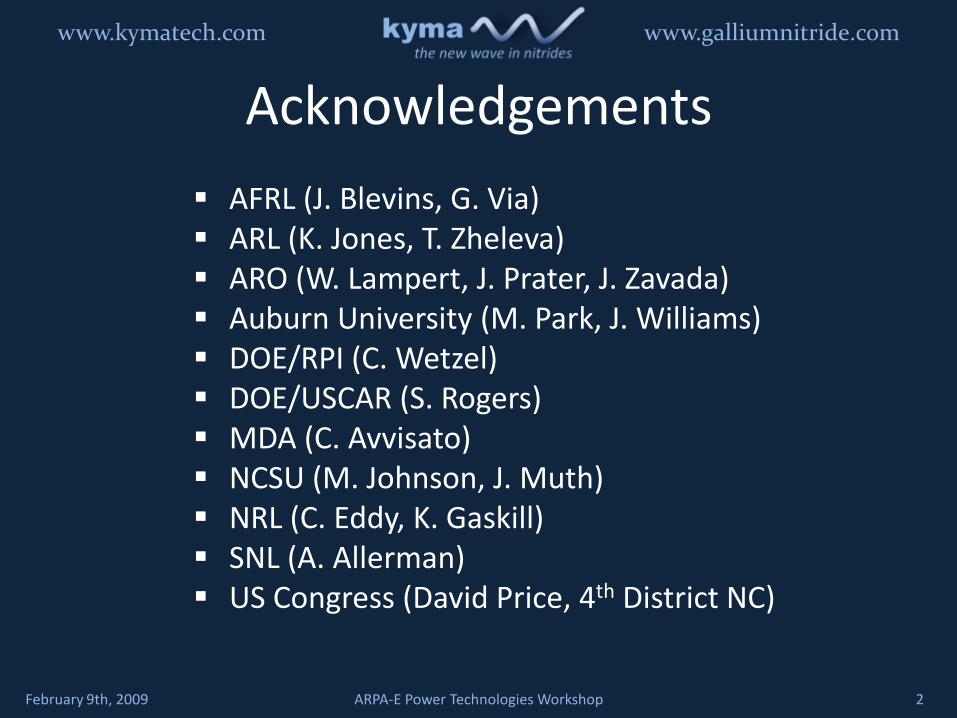
Acknowledgements
AFRL (J. Blevins, G. Via) ARL (K. Jones, T. Zheleva) ARO (W. Lampert, J. Prater, J. Zavada) Auburn University (M. Park, J. Williams) DOE/RPI (C. Wetzel) DOE/USCAR (S. Rogers) MDA (C. Avvisato) NCSU (M. Johnson, J. Muth) NRL (C. Eddy, K. Gaskill) SNL (A. Allerman) US Congress (David Price, 4th District NC)
February 9th, 2009 ARPA-E Power Technologies Workshop 2

www.kymatech.com www.galliumnitride.com
Motivating Statements & Questions
GaN will become
very important!
We will just buy GaN power
switches from Japan
Who will pay for bulk GaN’s
development?
Who will be the winners?
Who will be the losers?
We always wait till DOD
develops a new material device
combination
February 9th, 2009 ARPA-E Power Technologies Workshop
Power Electronics SpecialistUS Car Manufacturer
US DOE Technologist WBGS Industry Guru
3
www.kymatech.com www.galliumnitride.com
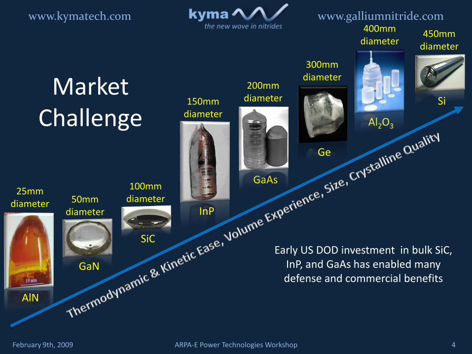
Ge
300mm diameterMarket
Challenge
SiC
GaAs
InP
Si
GaN
AlN
25mm diameter 50mm
diameter
100mm diameter
150mm diameter
200mm diameter
Al2O3
400mm diameter
450mm diameter
February 9th, 2009 ARPA-E Power Technologies Workshop
Early US DOD investment in bulk SiC, InP, and GaAs has enabled many defense and commercial benefits
4

www.kymatech.com www.galliumnitride.com
Major foreign interest in bulk & template GaN substrate technology
Next generation HEV needs >106 bulk GaN substrates/year
February 9th, 2009 ARPA-E Power Technologies Workshop 5

www.kymatech.com www.galliumnitride.com
Baliga’s Figure of Merit (BFOM)
Considers on resistance & break down voltage
3
24
CnSON E
VRµε
b=
CnS EBFOM µε=
Reduced defect density

www.kymatech.com www.galliumnitride.com
R. W. Keyes, "Figure of Merit for Semiconductors for High Speed Switches,“ Proc. IEEE, vol. 60, pp. 225-232, 1972 B. J. Baliga, "Semiconductors for High-Voltage, Vertical Channel Field-Effect Transistors,“ J.Appl.Phys., vol. 53, no. 3, pp. 1759-1764, 1982
B.J. Baliga, “Power semiconductor device figure of merit for high – frequency applications,” IEEE Electron Device Lett., vol. 10, pp. 455-457, 1989T. Ayalew, “SiC Semiconductor Devices, Technology, Modeling, and Simulation,” http://www.iue.tuwien.ac.at/phd/ayalew/node76.html
Figure of Merit Expression
Combined (General) kthεµevsEc2
Keyes (Power Density & Speed) kth [c vs / (4πεs)]-1/2
Baliga FOM (Resistive Losses) εµeEg3
Baliga High Frequency FOM (Switching Losses) µeEb2
Factor Si SiC GaNBaliga Figure of Merit 1 223 868
Dislocation Density (cm-2) < 1 103 104 -106
Micropipe Density (cm-2) 0 30 0
Stacking Fault Energy (mJ/m2) 55 14.7 20Crystalline Polytypes 1 >245 2
Diameter 12” 4” 2”
εs is the static dielectric constant
µ is the mobility
Eg is the bandgap
Vg is the gate drive voltage
Eb is the breakdown field
February 9th, 2009 ARPA-E Power Technologies Workshop
An additional advantage of GaN
over Si and SiC is the ability to bandgap
engineer via growth of epitaxial
heterostructures
NCSU & Georgia Tech7
www.kymatech.com www.galliumnitride.com
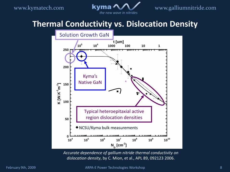
Accurate dependence of gallium nitride thermal conductivity on dislocation density, by C. Mion, et al., APL 89, 092123 2006.
Thermal Conductivity vs. Dislocation Density
February 9th, 2009 8ARPA-E Power Technologies Workshop
0
50
100
150
200
250
104 105 106 107 108 109 1010
1101001000104105
K [W
.K-1
m-1
]
ND [cm-2]
t [um]
NCSU/Kyma bulk measurements
Typical heteroepitaxial active region dislocation densities
Kyma’s Native GaN
Solution Growth GaN

www.kymatech.com www.galliumnitride.com
Accurate dependence of gallium nitride thermal conductivity on dislocation density, by C. Mion, et al., APL 89, 092123 2006.
100
150
200
250
300
350
1.E+03 1.E+04 1.E+05 1.E+06 1.E+07 1.E+08 1.E+09 1.E+10
Ther
mal
Con
duct
ivit
y (W
/K-m
)
Defect Density (cm-2)
Point Defect
Limited?
Dislocation Density Limited?
Crystal Process Challenge
Thermal Conductivity vs. Dislocation Density
February 9th, 2009 9ARPA-E Power Technologies Workshop

www.kymatech.com www.galliumnitride.com
February 9th, 2009 ARPA-E Power Technologies Workshop
From: Johnson et al., IEEE Trans. Electron Dev., 49, 32 (2002).)
Un-passivated, simple Schottky diode demonstration, from
collaboration with NCSU (Mark Johnson), Auburn University
(Minseo Park), & Sandia National Laboratories (Andy
Allerman)
10

www.kymatech.com www.galliumnitride.com
Native GaN Substrate Progress
Single wafers BoulesMitsubishi Chemicals
Kyma TechnologyKyma Technology
Hitachi Cable
WS-1 “Substrates for Nitride Epitaxy” IWN2008, Switzerland 2008February 9th, 2009 ARPA-E Power Technologies Workshop 11

www.kymatech.com www.galliumnitride.com
8mm x 25mm GaN boule with TDD
~103cm-2
R. Kucharski, et. al, APL 95 (2009) 131119
0.5mm x 30mm GaN substrate with TDD ~1E6cm-2
February 9th, 2009 ARPA-E Power Technologies Workshop 12

www.kymatech.com www.galliumnitride.com
Comparing Bulk GaN Crystal Growth Technologies
HVPE Bulk GaN They grow quite fast and
thick However not too smooth One really needs a trick To make them really good It seems that what they
need To grow in perfect way It's just a perfect seed Available some day
Ammonothermal Bulk GaN
What does ammono show
That crystals really grow
Although the growth is slow
They have not any bow
Source: http://www.unipress.waw.pl/iwbns6/fun-concl.html
February 9th, 2009 ARPA-E Power Technologies Workshop
From Iza Grzegory’s Poem Based on 6th International Workshop on Bulk Nitride Semiconductors
13

www.kymatech.com www.galliumnitride.com
Comparing Bulk GaN Crystal Growth Approaches
Qualitative Feature vs. Growth Approach HVPE AMT
AMT on HVPE Seed
HVPE on AMT Seed
Growth Rate
Electrical Conductivity Control
Seed Generating Potential
Growth Parameters (P, T)
Time to Market
Substrate Quality
*Bulk GaN Process Figure of Merit (+) 21 11 9 24
*Bulk GaN Process Figure of Merit (x) 1536 12 6 4096
February 9th, 2009 ARPA-E Power Technologies Workshop
*FOM Calculation Assumes = 4, = 3, = 2, = 1
14
www.kymatech.com www.galliumnitride.com
Summary & Conclusions GaN’s importance will grow and grow
• GaN is 2nd only to Silicon in importance• Bulk GaN will become cheap and readily available
Unfettered access to bulk GaN will drive device and system innovation of unprecedented long term importance• The market will support only a few winners
Major US investment in bulk GaN represents a great opportunity that cannot be overlooked
February 9th, 2009 ARPA-E Power Technologies Workshop 15
Related Documents