Built-In Self Test for Regular Structure Embedded Cores in System-on-Chip Except where reference is made to the work of others, the work described in this thesis is my own or was done in collaboration with my advisory committee. This thesis does not include proprietary or classified information. Srinivas Murthy Garimella Certificate of Approval: Victor P. Nelson Professor Electrical and Computer Engineering Charles E. Stroud, Chair Professor Electrical and Computer Engineering Adit D. Singh Professor Electrical and Computer Engineering Stephen L. McFarland Acting Dean Graduate School

Welcome message from author
This document is posted to help you gain knowledge. Please leave a comment to let me know what you think about it! Share it to your friends and learn new things together.
Transcript

Built-In Self Test for Regular Structure Embedded Cores in
System-on-Chip
Except where reference is made to the work of others, the work described in thisthesis is my own or was done in collaboration with my advisory committee. This
thesis does not include proprietary or classified information.
Srinivas Murthy Garimella
Certificate of Approval:
Victor P. NelsonProfessorElectrical and Computer Engineering
Charles E. Stroud, ChairProfessorElectrical and Computer Engineering
Adit D. SinghProfessorElectrical and Computer Engineering
Stephen L. McFarlandActing DeanGraduate School
Built-In Self Test for Regular Structure Embedded Cores in
System-on-Chip
Srinivas Murthy Garimella
A Thesis
Submitted to
the Graduate Faculty of
Auburn University
in Partial Fulfillment of the
Requirements for the
Degree of
Master of Science
Auburn, Alabama
May 13, 2005

Built-In Self Test for Regular Structure Embedded Cores in
System-on-Chip
Srinivas Murthy Garimella
Permission is granted to Auburn University to make copies of this thesis at itsdiscretion, upon the request of individuals or institutions and at their expense.
The author reserves all publication rights.
Signature of Author
Date
Copy sent to:
Name Date
iii
Vita
Srinivas Murthy Garimella, son of Satyanarayana and Subhadra Garimella, was
born on August 29 1980 in Vijayawada, India. He graduated with distinction with
a Bachelor of Technology in Electronics and Communications Engineering degree in
May 2002 from Jawaharlal Nehru Technological University, Hyderabad, India. After
completion of his undergraduate degree, he joined Tata Consultancy Services (TCS),
India as Assistant Systems Engineer in June 2002. He entered the graduate program
in Electrical and Computer Engineering at Auburn University in August 2003. While
in pursuit of his Master of Science degree at Auburn University, he worked under the
guidance of Dr. Charles E. Stroud as a graduate student assistant in the Electrical
and Computer Engineering Department.
iv

Thesis Abstract
Built-In Self Test for Regular Structure Embedded Cores in
System-on-Chip
Srinivas Murthy Garimella
Master of Science, May 13, 2005(B.Tech., Jawaharlal Nehru Technological University, Hyderabad, India. May 2002)
109 Typed Pages
Directed by Charles Stroud
Miniaturization and integration of different cores onto a single chip are increasing
the complexity of VLSI chips. To ensure that these chips operate as desired, they
have to be tested at various phases of their development. Built-In Self-Test (BIST)
is one technique which allows testing of VLSI chips from wafer-level to system-level.
The basic idea of BIST is to build test circuitry inside the chip so that it tests
itself along with the BIST circuitry. The idea of current research is to develop BIST
configurations for testing memory cores and other regular structure cores in Field
Programmable Gate Arrays (FPGAs) and System-on-Chips (SoCs).
FPGA-independent BIST approach for testing memory cores and other regular
structure cores in FPGAs is described in this thesis. BIST configurations were devel-
oped to test memory cores in Atmel and Xilinx FPGAs using this approach. Another
approach which takes advantage of some of the architectural capabilities of Atmel
SoCs to reduce test time is also described in this thesis.
v

Acknowledgments
I would like to thank Dr. Stroud for his support and advice throughout my
research at Auburn University. I would also like to thank Dr. Nelson and Dr. Singh
for being on my graduate committee and for their contribution to my thesis. I would
like to acknowledge my research colleagues John, Jonathan, Sachin and Sudheer for
their help and inspirational discussions during my research. Finally I would like to
express my deepest gratitude to my parents whose love and encouragement is inspiring
me to achieve my goals.
vi
Style manual or journal used LATEX– A Document Preparation System, Leslie
Lamport, Addison-Wesley Publishing Company, 2nd edition (1994). Bibliography
follows IEEE Transactions.
Computer software used The document preparation package TEX (specifically
LATEX) together with the departmental style-file aums.sty. The plots were generated
using Microsoft Excel®. Images drawn using Microsoft®Visio®.
vii

Table of Contents
List of Figures x
List of Tables xii
1 Introduction 11.1 System-on-Chip (SoC) . . . . . . . . . . . . . . . . . . . . . . . . . . 11.2 CSOC Architecture . . . . . . . . . . . . . . . . . . . . . . . . . . . . 31.3 FPGAs . . . . . . . . . . . . . . . . . . . . . . . . . . . . . . . . . . . 31.4 Embedded Memories . . . . . . . . . . . . . . . . . . . . . . . . . . . 51.5 Built-In Self-Test (BIST) . . . . . . . . . . . . . . . . . . . . . . . . . 61.6 BIST for SoC . . . . . . . . . . . . . . . . . . . . . . . . . . . . . . . 81.7 Thesis Statement . . . . . . . . . . . . . . . . . . . . . . . . . . . . . 8
2 Background 122.1 System on a Chip (SoC) . . . . . . . . . . . . . . . . . . . . . . . . . 122.2 FPGA Architectures . . . . . . . . . . . . . . . . . . . . . . . . . . . 13
2.2.1 Switching Elements in FPGAs . . . . . . . . . . . . . . . . . . 152.2.2 PLB Architecture . . . . . . . . . . . . . . . . . . . . . . . . . 17
2.3 Embedded Memories . . . . . . . . . . . . . . . . . . . . . . . . . . . 212.3.1 Memory Types . . . . . . . . . . . . . . . . . . . . . . . . . . 222.3.2 Embedded Memories in FPGAs . . . . . . . . . . . . . . . . . 222.3.3 Embedded Memories and FPGAs in SoCs and their Interfacing 28
2.4 BIST for Memories . . . . . . . . . . . . . . . . . . . . . . . . . . . . 322.4.1 Present Methods for Testing FPGAs and SoCs . . . . . . . . . 35
2.5 Thesis Restatement . . . . . . . . . . . . . . . . . . . . . . . . . . . . 38
3 Implementation Of BIST On ATMEL FPGAs And SoCs 403.1 RAM BIST Approaches . . . . . . . . . . . . . . . . . . . . . . . . . 40
3.1.1 BIST Approach for Free RAMs Using FPGA Logic . . . . . . 413.1.1.1 BIST Architecture for Dual-port Synchronous Mode 413.1.1.2 BIST Architecture for Single-port Modes . . . . . . . 44
3.1.2 Advantages and Limitations of Using VHDL . . . . . . . . . . 473.1.3 BIST Approach for Free RAMs Using Embedded Processor Core 51
3.1.3.1 AVR-FPGA Interface Description . . . . . . . . . . . 513.1.3.2 BIST Architecture . . . . . . . . . . . . . . . . . . . 533.1.3.3 Implementation of BIST Approach in FPSLIC . . . . 53
3.1.4 On-Chip Diagnostics . . . . . . . . . . . . . . . . . . . . . . . 56
viii

3.2 Data SRAM Testing . . . . . . . . . . . . . . . . . . . . . . . . . . . 593.3 Summary . . . . . . . . . . . . . . . . . . . . . . . . . . . . . . . . . 62
4 Implementation of BIST on Xilinx FPGAs 664.1 Motivation . . . . . . . . . . . . . . . . . . . . . . . . . . . . . . . . . 664.2 PLB and Routing Architecture . . . . . . . . . . . . . . . . . . . . . 674.3 Embedded Block RAMs Architecture . . . . . . . . . . . . . . . . . . 694.4 Block RAM Testing . . . . . . . . . . . . . . . . . . . . . . . . . . . . 71
4.4.1 Block RAM Testing in Single-port Mode . . . . . . . . . . . . 734.4.1.1 BIST Implementation . . . . . . . . . . . . . . . . . 754.4.1.2 Diagnosis . . . . . . . . . . . . . . . . . . . . . . . . 78
4.4.2 Block RAM Testing in Dual-port Mode . . . . . . . . . . . . . 784.5 Summary of Block RAM Testing . . . . . . . . . . . . . . . . . . . . 794.6 LUT RAM Testing . . . . . . . . . . . . . . . . . . . . . . . . . . . . 80
4.6.1 BIST Implementation . . . . . . . . . . . . . . . . . . . . . . 814.7 MULTIPLIER BIST . . . . . . . . . . . . . . . . . . . . . . . . . . . 83
5 Summary and Conclusions 855.1 Summary . . . . . . . . . . . . . . . . . . . . . . . . . . . . . . . . . 855.2 Observations . . . . . . . . . . . . . . . . . . . . . . . . . . . . . . . . 875.3 Future Research . . . . . . . . . . . . . . . . . . . . . . . . . . . . . . 89
Bibliography 91
Appendices 97
A ASL code for free RAM 98
B VHDL Code for March Y algorithm 103
C March LR Algorithm for Block RAMs 108C.1 March LR Algorithm with BDS for 16-bit Wide RAMs . . . . . . . . 108C.2 RAMBISTGEN Input File Format for Generating VHDL Code . . . . 108
ix

List of Figures
1.1 Evolutionary Stages of System-on-Chip Products . . . . . . . . . . . 2
1.2 Typical Architecture of a CSOC . . . . . . . . . . . . . . . . . . . . . 3
1.3 Architecture of a Typical FPGA . . . . . . . . . . . . . . . . . . . . . 4
1.4 BIST Architecture . . . . . . . . . . . . . . . . . . . . . . . . . . . . 7
2.1 Switching Elements Used in FPGAs . . . . . . . . . . . . . . . . . . . 15
2.2 FPGA Programming Controlled by SRAM Cells . . . . . . . . . . . . 18
2.3 Atmel AT40K Series PLB . . . . . . . . . . . . . . . . . . . . . . . . 19
2.4 PLB Array Interconnection in Atmel AT40K Series FPGAs . . . . . . 21
2.5 Structure of Memory Cells . . . . . . . . . . . . . . . . . . . . . . . . 23
2.6 Arrangement of Free RAMs in Atmel AT40K Series FPGAs . . . . . 24
2.7 Architecture of a Free RAM Block . . . . . . . . . . . . . . . . . . . 25
2.8 Block Diagram of Spartan II Family FPGAs . . . . . . . . . . . . . . 27
2.9 Block Diagram of a Block RAM . . . . . . . . . . . . . . . . . . . . . 29
2.10 Embedded SRAM in Atmel’s FPSLIC . . . . . . . . . . . . . . . . . . 30
2.11 Partitioning of Embedded SRAM in Atmel’s FPSLIC . . . . . . . . . 31
2.12 AVR-FPGA-RAM Interface in Atmel’s FPSLIC . . . . . . . . . . . . 32
2.13 AVR-FPGA Cache Logic in Atmel’s FPSLIC . . . . . . . . . . . . . . 33
2.14 BIST Architecture for Testing PLBs in FPGAs . . . . . . . . . . . . 37
3.1 Dual-port Free RAM BIST Architecture and ORA Design . . . . . . 42
3.2 Single-port Free RAM BIST Architecture and ORA Design . . . . . . 45
x

3.3 Fault Simulation Results for Free RAM . . . . . . . . . . . . . . . . . 47
3.4 Snapshot of The RAMBISTGEN Tool . . . . . . . . . . . . . . . . . 49
3.5 AVR-FPGA Interface . . . . . . . . . . . . . . . . . . . . . . . . . . . 52
3.6 Architecture of RAMBIST From AVR . . . . . . . . . . . . . . . . . 53
3.7 RAMBIST Implementation from AVR . . . . . . . . . . . . . . . . . 54
3.8 Three Configurations for Data SRAM testing . . . . . . . . . . . . . 60
4.1 Architecture of a Slice in Virtex and Spartan FPGAs . . . . . . . . . 68
4.2 Organization of Block RAMs in Various Xilinx FPGAs . . . . . . . . 70
4.3 Block Diagram of a Block RAM . . . . . . . . . . . . . . . . . . . . . 72
4.4 BIST Architecture for Block RAMs Testing . . . . . . . . . . . . . . 73
4.5 Block RAM Configuration for Testing both Ports in Single-port Mode 74
4.6 Design of a Single-bit ORA for Block RAM Testing . . . . . . . . . . 76
4.7 Programmable Logic Resources in Xilinx FPGAs . . . . . . . . . . . 80
4.8 ORA Designs Used for LUT RAM Testing . . . . . . . . . . . . . . . 82
4.9 Multiplier Modes . . . . . . . . . . . . . . . . . . . . . . . . . . . . . 83
xi
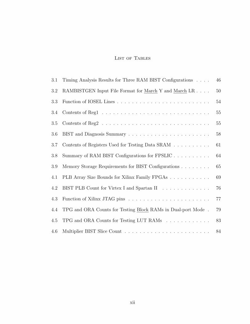
List of Tables
3.1 Timing Analysis Results for Three RAM BIST Configurations . . . . 46
3.2 RAMBISTGEN Input File Format for March Y and March LR . . . . 50
3.3 Function of IOSEL Lines . . . . . . . . . . . . . . . . . . . . . . . . . 54
3.4 Contents of Reg1 . . . . . . . . . . . . . . . . . . . . . . . . . . . . . 55
3.5 Contents of Reg2 . . . . . . . . . . . . . . . . . . . . . . . . . . . . . 55
3.6 BIST and Diagnosis Summary . . . . . . . . . . . . . . . . . . . . . . 58
3.7 Contents of Registers Used for Testing Data SRAM . . . . . . . . . . 61
3.8 Summary of RAM BIST Configurations for FPSLIC . . . . . . . . . . 64
3.9 Memory Storage Requirements for BIST Configurations . . . . . . . . 65
4.1 PLB Array Size Bounds for Xilinx Family FPGAs . . . . . . . . . . . 69
4.2 BIST PLB Count for Virtex I and Spartan II . . . . . . . . . . . . . 76
4.3 Function of Xilinx JTAG pins . . . . . . . . . . . . . . . . . . . . . . 77
4.4 TPG and ORA Counts for Testing Block RAMs in Dual-port Mode . 79
4.5 TPG and ORA Counts for Testing LUT RAMs . . . . . . . . . . . . 83
4.6 Multiplier BIST Slice Count . . . . . . . . . . . . . . . . . . . . . . . 84
xii

Chapter 1
Introduction
Since the arrival of the first transistor-based computer, high scale integration
became one of the main concerns in the hardware design techniques. In the early
1970’s relatively high levels of integration were achieved, but the continuing effort
to miniaturize and build more complex digital circuitry remained one of the goals
in leading computer construction and chip design [1]. As a result, semiconductor
integration has progressed from Small Scale Integration (SSI) to Very Large Scale
Integration (VLSI) and now to System Level Integration (SLI) or System-on-Chip
(SoC) [1].
1.1 System-on-Chip (SoC)
SoC technologies are the consequent continuation of the Application Specific
Integrated Circuit (ASIC) technology, whereas complex functions, that previously re-
quired heterogeneous components to be merged onto a printed circuit board, are now
integrated within one single silicon IC or chip [2]. As device integration scales grew,
the enhanced performance of memory, microprocessors and logic devices boosted the
performance of the digital systems they constituted. However, performance increases
in larger systems were hampered by speed limitations associated with the long and
numerous interconnects between devices on the printed circuit board (PCB) and as-
sociated input/output (I/O) buffers on the chips. Closely related system functions
must be combined on a single chip to eliminate this bottleneck and take full advantage
1

of improvements in transistor switching speeds and higher integration scales. This is
precisely the capability that SoC technology provides. Rapid advances in semicon-
ductor processing technologies allowed the realization of complicated designs on the
same IC. Figure 1.1 illustrates the evolutionary stages toward SoC products.
(a) Multi-board systems (c) System-on-Chip products
(b) Single-board systems
DRAM/FlashMemory
CPU/Cache/Interface
3D Graphics
DR
AM
/Fla
sh M
emor
y
CPU/Cache
3D Graphics
Interface/Logic
MPEG
DSP
Figure 1.1: Evolutionary Stages of System-on-Chip Products
SoCs can be broadly classified into two categories: ASIC-based and Configurable
or Programmable. While the Configurable SoCs (CSoC) can be customized to dif-
ferent applications through embedded reconfigurable logic cores, ASIC-based SoCs
cannot be customized. CSoCs combine the advantages of both ASIC-based SoCs and
multi-chip board development using standard components [1]. The major general
goal for the development of such application-tailored reconfigurable architectures is
to realize adaptivity vs. power/performance/cost trade-offs by migrating functional-
ity from ASICs to multi-granularity reconfigurable hardware [3].
2

1.2 CSOC Architecture
The typical architecture of a CSoC is as shown in Figure 1.2. A CSoC consists
of a dedicated microcontroller core and other components built around a common bus
system. Required applications can be designed using microcontroller, DSP core or
other Intellectual Property (IP) cores. The reconfigurable logic core typically consists
of a low power Field Programmable Gate Array (FPGA). Embedded memories also
form a large portion of the CSoC [4] [5].
Reconfigurable Logic
(FPGA)On-Chip Memory Micro Controller
DSP Core Other IP Cores
Common Bus System
Figure 1.2: Typical Architecture of a CSOC
1.3 FPGAs
FPGAs are flexible alternatives to custom ICs. FPGAs can be programmed by
the end users at their site. Moreover they can be reprogrammed any number of times.
3

Since FPGAs bring short time-to-market and flexibility for systems using digital logic
circuits, many applications have been developed in order to make best use of FPGA
reprogrammability. FPGAs can implement both combinational and sequential logic
of tens of thousands of gates.
PLB PLB PLB
PLB PLB PLB
PLB PLB PLB
IOB
Interconnect Network
Figure 1.3: Architecture of a Typical FPGA
A typical FPGA architecture usually includes three categories of user programmable
elements as shown in Figure 1.3 . Programmable Logic Blocks (PLBs), Input Out-
put Blocks (IOBs) and programmable interconnection network. PLBs are sometimes
called Configurable Logic Blocks (CLBs). An interior array of PLBs provides the
functional elements from which the user’s logic is constructed, while IOBs provide
4
an interface between the logic array and device package pins. The programmable
interconnect network provides routing paths to connect the inputs and outputs of the
PLBs and IOBs [6]. The functionality of these three types of programmable elements
is controlled by the configuration memory in the FPGA.
The FPGA provides a generic chip that can be programmed for any application
by downloading a desired configuration into the configuration memory of the FPGA.
This dictates the behavior of the underlying hardware (PLBs, IOBs and interconnect
network). The programming data takes the form of a bit-stream consisting of a string
of binary 1s and 0s and is stored in the configuration memory. These configuration
memory bits are then used on-board the FPGA to control the on-off state of vari-
ous pass transistors and multiplexers to program the PLBs, IOBs and interconnect
elements [7].
Improvements in process technology have had a significant impact on the archi-
tecture of FPGAs. Traditionally FPGAs were targeted to implement smaller logic
circuits. Recently, FPGAs are being used to implement relatively large circuits and
systems. Since the large systems often require data storage, large on-chip memories
have become an essential component of high-density FPGAs [8] [9]. These memory
arrays can also be configured as Read Only Memories (ROMs) to implement large
combinational logic functions.
1.4 Embedded Memories
SoCs are moving from logic-dominant chips to memory-dominant chips. Large
amounts of Static Random Access Memory (SRAM), ROM, Erasable Programmable
5
Read-Only Memory (EPROM) and multi-port RAMs are finding their way on board.
According to the International Technology Roadmap for Semiconductors [10] memo-
ries will cover 90 percent of the SoC die area by 2010. Because of their high density,
embedded memories are more prone to defects that already exist in silicon than any
other component on the chip [11]. Increasing the memory on a SoC complicates the
manufacturing processes and reduces yield, adding to the cost of the SoC. Therefore
from a testability point of view, it is essential to thoroughly test memories in the
SoCs [12].
1.5 Built-In Self-Test (BIST)
Traditionally chips were tested using Automatic Test Equipment (ATE). Tests
ranged from those developed manually to those generated automatically for scan-
based designs. Scan is a Design for Test (DFT) technique whereby all internal storage
elements are modified so that in test mode they form individual stages of a shift
register for scanning test data in and test responses out. The use of Automatic
Test Pattern Generation (ATPG) programs to generate manufacturing tests for VLSI
designs became popular in the early 1980s. Soon, it was also recognized that test
circuitry must be added to a design to simplify ATPG [13].
As the complexity and size of ICs grew, test equipment became more sophisti-
cated increasing the manufacturing cost to as much as 30 to 40 percent of the cost of
production [14]. Because of the limitations of the conventional testing techniques, a
new DFT technique called Built-In Self-Test (BIST) was developed.
6

BIST Controller
Test Pattern Generator (TPG)
Circuit under Test (CUT)
Output Response Analyzer (ORA)
Figure 1.4: BIST Architecture
BIST is a DFT technique in which testing is accomplished through built-in hard-
ware features [15]. The basic idea is to have a VLSI chip that tests itself. The typical
BIST architecture is composed of three hardware modules in addition to the circuit
under test (CUT), as shown in Figure 1.4. The Test Pattern Generator (TPG) gener-
ates the test patterns for the CUT. The Output Response Analyzer (ORA) compares
or analyzes the test responses to determine correctness of the CUT. The BIST con-
troller is the central unit to control all the BIST operations including initialization
and length of the BIST sequence. In a BIST system hierarchy, there are BIST con-
trollers at each level of the circuit hierarchy, such as module, chip, board, and system
levels. Each BIST controller is responsible for the self-test in that particular level,
the control of BIST operations for the lower level BIST, and the reporting of the test
results to the upper level. The design of a TPG is determined by the test strategy
7

being deployed. The test strategy being selected is determined by the fault coverage,
test hardware overhead, and testing time [15].
1.6 BIST for SoC
The major advantages of the Configurable SoC (CSoC) technique are a short
time to market due to pre-designed cores, less cost due to reusability of cores, a
higher performance using optimized algorithms and less hardware area using opti-
mized designs. But the SoC technique also introduces new difficulties into the test
process caused by the increased complexity of the chip, the reduced accessibility of
the cores and the higher heterogeneity of the modules. In the SoC test process, a core
test strategy has to be determined first. Then a SoC test strategy has to be selected
where the test access for individual cores is determined and the tests are integrated
at the system level. All these tasks are simplified if the cores and the entire system
support a BIST strategy [16].
1.7 Thesis Statement
Many of today’s chips demand more embedded memory than ever before. SoCs
and FPGAs are also moving from logic-dominant to memory-dominant chips. The
addition of memory, while it creates a more powerful chip, increases die size and
results in poor yield. As the percentage of embedded memory continues to increase,
so does the chip’s complexity, density, speed and of course, the probability of failures
due to wafer defects. For SoCs to keep up their momentum and remain a viable
8

option for improving system integration and performance, the problems relating to
testing multiple high-density, multi-megabit memories must be solved [11].
Embedded memories placed on a single chip are scattered around the device and
typically have different types (SRAM, DRAM), sizes, access protocols, and timing.
Since on-chip field-configurable memory provides significant memory bandwidth com-
pared to off-chip memory, memories are embedded into more recent FPGAs as well
as into CSoCs. Typically, these FPGAs contain heterogeneous memory architecture,
that is, architecture with more than one size of memory array. Due to reprogamma-
bility of FPGAs, it has been proposed that BIST capabilities can be configured in
an FPGA to completely test the embedded memories in FPGAs and other memory
cores shared by the FPGAs [17].
In this thesis, two approaches are described for testing embedded memories in
FPGAs and SoCs. The first approach aims at reducing the BIST development time
when generating BIST configurations for testing memories in different FPGA devices.
The second approach aims at reducing the total test-time. The first approach is
partly based on the BIST for FPGAs method in [18] [19]. In this approach, some
of the PLBs of the FPGA are configured as TPGs and ORAs to test the embedded
memory. Unlike the traditional BIST for FPGAs, the basic approach here consists
of developing parameterized VHDL code for testing embedded memories of various
sizes and various types.The VHDL Code is then synthesized using Computer Aided
Design (CAD) tools to generate bit-streams. The bit-streams are then downloaded
to configure the FPGA to test embedded memories. This approach is used in stand-
alone FPGAs which do not have the capability of dynamic partial reconfiguration.
9
This VHDL approach has an added advantage of portability. This reduces BIST
development time for generating BIST configuration for testing different types and
sizes of memory cores in different FPGAs. The VHDL approach was applied to
test memory modules in Atmel AT40K series FPGAs. The same VHDL code was
used with minimal changes for testing memory modules in Xilinx Virtex and Spartan
series FPGAs. Similar approaches can be used for testing other regular structure
embedded cores in FPGAs. This approach was used to test embedded multipliers in
Xilinx Virtex and Spartan series FPGAs.
For FPGA cores embedded in SoCs, which can be dynamically configured, a
different approach is adopted. The embedded microcontroller can be used to test the
embedded memories in FPGAs. The microcontroller can dynamically reconfigure the
memories to a different configuration mode and apply test patterns while PLBs are
used to perform the ORA functions. This process is repeated until all memories are
tested in all possible configurations. For testing other memory cores accessible only
by the microcontroller, the microcontroller can be used to perform both TPG and
ORA functions. The proposed BIST methodologies are verified by testing embedded
memories in Atmel’s Field Programmable System Level Integrated Circuit (FPSLIC)
and Xilinx Virtex and Spartan series FPGAs.
This thesis is organized as follows: Chapter 2 gives a more detailed description
of the architecture of FPGAs and memories as well as existing BIST methodologies
for testing FPGAs and embedded memories. Chapter 3 presents the architecture,
implementation details and experimental results of the proposed BIST approaches
applied to test RAMs in the Atmel FPSLIC. Chapter 4 gives implementation details
10

and experimental results of the proposed BIST method applied to test RAMs in Virtex
and Spartan series FPGAs. The thesis is summarized in Chapter 5 with suggestions
for future research.
11
Chapter 2
Background
This chapter presents an overview of the SoCs, architecture of the FPGAs and
the memories that served as target for this thesis research. The interface of FPGA
core, memory core and processor core in the Atmel AT94K SoC is described. Also the
architecture of RAMs in Virtex and Spartan FPGAs is discussed. Finally, previous
BIST methodologies for testing FPGAs and embedded memories are presented.
2.1 System on a Chip (SoC)
From its introduction in the 1990s, the SoC has gone through many phases.
Early SoCs consisted of a central processor, memory, and random or glue logic. Glue
logic was used by designers to connect the cores to make the SoC meet a set of design
specifications. Current SoCs comprise one or more processing blocks (microproces-
sors, DSP cores), communication cores, memory blocks (SRAM, DRAM, flash, etc.),
random logic, analog functions and often configurable logic [20].
The architecture of most of the current SoCs is processor driven. The central
processor in a SoC manages IP cores, on-chip memory, I/O and is thus responsible for
overall system supervision [5]. The microprocessor communicates with all other cores
through one or more on-chip busses. An alternative concept of the logic centric archi-
tecture is discussed in [21]; where in an embedded processor would be an additional
system component rather than a central component. The logic centric architecture
focuses on making programmable logic a central architectural feature.
12

Most configurable SoCs, also called CSoCs, support programmable logic in the
form of an embedded FPGA core. Embedded FPGAs can be used to reconfigure on-
chip functionality after chip fabrication. FPGAs can be used to correct any design
errors that could have occurred during chip development and also to upgrade products
to adapt to changing requirements. FPGAs are thus becoming essential components
of current SoCs. Different kinds of stand-alone FPGAs and their architectures are
discussed in the subsequent section [21].
2.2 FPGA Architectures
Digital logic can be implemented using either discrete logic devices (often called
Small-Scale Integrated circuits or SSI), Programmable Logic Devices (PLDs), Masked-
Programmed Gate Arrays (MPGAs), or FPGAs. SSI is used for implementing small
amounts of logic. A PLD is a general purpose device capable of implementing the logic
as two-level sum-of-products of its inputs. Power consumption and delay typically
limit its usage to implementation of eight to sixteen product terms. To implement
designs with thousands or tens of thousands of gates on a single IC, MPGAs (com-
monly called gate arrays) can be used. An MPGA consists of a base of pre-designed
transistors with customized wiring added for each design. The wiring is built dur-
ing the manufacturing process such that each design requires custom masks for the
wiring. The mask-making charges make low-volume MPGAs expensive [20].
FPGAs offer benefits of both PLDs and gate arrays. Like MPGAs, FPGAs
can implement large designs on a single IC. FPGAs, however, eliminate each design’s
custom masking, manufacturing, test pattern generation, wafer fabrication, packaging
13

and testing when compared to MPGAs [20]. Like PLDs, FPGAs are programmable
by designers at their site. FPGAs are however a step above Programmable Logic
Devices (PLDs) in complexity [7]. This is so because FPGAs can implement multilevel
logic, while most PLDs are optimized for two-level logic [22]. Thus FPGAs offer
advantages over MPGAs of low Non-Recurring Engineering (NRE) costs and rapid
turn-around time. However, the overhead of programming circuitry that manages the
programming part of the FPGAs reduces its density. Moreover, the programmable
switches in the FPGA increases signal delay. As a result, FPGAs are larger and
slower than equivalent MPGAs [20].
FPGAs are composed of an array of PLBs interconnected with a programmable
routing network. The size, structure and number of PLBs as well as the amount of
interconnect vary considerably among FPGA architectures. This difference is gov-
erned by different programming technologies and different target applications of the
devices. Switching elements used for programming determine whether the FPGA is
antifuse-programmed, EPROM-programmed or SRAM-programmed. Depending on
routing structure, FPGAs can be further classified as Symmetrical style, Island style
and Cellular style [22]. Depending on cell granularity, FPGAs can be classified as
either coarse grained or fine grained. Granularity of a PLB can be defined in many
ways: number of boolean functions that can be implemented by it, total number of
transistors it uses, total number of inputs and outputs, total normalized area, etc.
Since the switching elements are the driving force in determining the choice of logic
modules and interconnect for FPGA, they become a key to FPGA architecture [20].
14

Different switching elements used in manufacturing FPGAs are examined in the next
subsection.
2.2.1 Switching Elements in FPGAs
In anti-fused programmed FPGAs, anti-fuses are used as switching elements. An
anti-fuse as shown in Figure 2.1(a) is a two terminal device that changes irreversibly
from a high to low resistance state when a programming voltage is applied across its
terminals [23]. Anti-fuse falls into two categories: amorphous silicon and dielectric.
Major advantages of the Anti-fuse are its small size, relatively low on-resistance and
low parasitic capacitance [24]. The major disadvantages of anti-fuse are that it is not
reprogrammable and it requires extra fabrication steps [24].
select gate
floating gate
SRAMcell
W1
W2
dielectric
A B
(a) Antifuse (b) EPROM (c) SRAM
pull-up resistor
bit line
word line
Figure 2.1: Switching elements used in FPGAs [24]
15

Switching elements used by EPROM-programmed FPGAs are similar to the
ones used in EPROM memories as shown in Figure 2.1(b). Unlike a simple Metal
Oxide Semiconductor (MOS) transistor, an EPROM transistor comprises two gates,
a floating gate and a select gate. In the un-programmed state, no charge exists on
the floating gate and the transistor behaves like a normal MOS transistor. When the
transistor is programmed by causing a large current to flow between source and drain,
a charge is trapped under the floating gate which permanently turns the transistor
off. The EPROM transistor can be reprogrammed by first removing the trapped
charge from the floating gate by exposing the gate to ultraviolet light [23]. A major
advantage of this technology compared to anti-fuse is its reprogrammability. An
additional advantage is that it is nonvolatile such that no external permanent memory
is needed to program the chip on power-up. Disadvantages associated with this
technology include relatively high on resistance, requirement of additional fabrication
steps over the ordinary CMOS fabrication process [24]. EPROM transistors, however,
cannot be reprogrammed in-circuit. Electrically Erasable and Programmable ROM
(EEPROM) technology, which is similar to EPROM technology, can be reprogrammed
in-circuit. EEPROM technology, however, consumes about twice the chip area as
EPROM transistors and requires multiple voltage sources for reprogramming [25].
The Static RAM (SRAM) programming technology uses SRAM cells to control
pass gates and multiplexers as shown in Figure 2.1(c). A logic one stored in an
SRAM cell closes the pass gate and a logic zero stored in an SRAM cell opens the
pass gate. A major advantage of this approach is that SRAM cells can be programmed
in-circuit and require only standard integrated circuit process technology [24]. Thus
16

SRAM programmable FPGAs take advantage of process improvements driven by
semiconductor memories. A major disadvantage of SRAM programming technology
is its large area. It takes at least five transistors to implement an SRAM cell, plus
at least one transistor to serve as a programmable switch. SRAM is volatile and
thus must be programmed or configured at the time of power-up. This requires
external permanent memory to provide the programming bit storage. Since SRAM-
based FPGAs implement logic in static gates, they consume very low power even
for large amounts of logic and have very low standby current. All these factors
have made SRAM-programmed FPGAs quite popular, and as a result, they have
become the largest selling FPGAs in the commercial market [26]. Architectures of
FPGAs discussed in the remainder of the thesis assuming that the FPGAs are SRAM
programmed unless otherwise specified.
2.2.2 PLB Architecture
PLBs, which form an important building block of the FPGA device, are capa-
ble of implementing both combinational and sequential logic. Combinational logic is
commonly implemented by an array of SRAM cells called the lookup table or LUT.
The LUT made of 2n SRAM cells is addressed by n inputs. A LUT shown in Figure
2.2(a) consists of 3 inputs and is capable of implementing all 28 different Boolean
functions of its inputs. When the FPGA is programmed, the truth table correspond-
ing to the boolean function to be implemented is loaded into the LUT. For example,
the LUT shown in Figure 2.2(a) would implement a 3-input XOR function assuming
the topmost location corresponds to highest address in this case. The inputs to the
17

LUT are logically equivalent such that changing the pin to which a signal is connected
may require rearrangement of the bits in the LUT. Multiplexers (MUXs) are often
placed at the inputs of the LUT, so that inputs to the LUT can come from any of the
routing resources. A 2-input MUX controlled by a SRAM cell is as shown in Figure
2.2(b). The number of inputs to the MUX can be increased with more SRAM cells
to act as select controls.
a
b
c
z
1
0
0
1
0
1
1
0
a) Look Up Table
a
bz
0
1
0/1
SRAM cell
b) Multiplexer
Figure 2.2: FPGA Programming Controlled by SRAM Cells
For implementing sequential logic, storage elements like edge-triggered flip-flops
or level-sensitive D latches are included. MUXs are included to control routing and
additional functionality inside the PLB. Thus a PLB generally consist of LUT(s),
MUX(s) and storage elements. The size and number of LUTs along with the num-
ber of storage elements defines the granularity of a PLB. More complex PLBs with
large LUTs, greater numbers of MUXs and storage elements comprise coarse grained
18

FPGAs. FPGAs with simpler PLBs are fine grained. An investigation on a range of
LUT sizes and their effect on the overall chip revealed that 3-input or 4-input LUTs
give best density for a wide range of PLBs [27].
The PLB inside Atmel’s AT40K series FPGA is shown in Figure 2.3 [28] [29].
The PLB consists of two 3-input LUTs, called X LUT and Y LUT. Functions of up to
four inputs can be implemented using the LUTs and MUXs. A Set/Reset D Flip-Flop
is provided for implementing sequential logic. Multiplexers are included for providing
a variety of functionalities like combinational logic, sequential logic, arithmetic and
DSP/multiplier modes [29].
X Y
8x1LUT
8x1LUT
D
Y
ClkReset
X
To/F
rom
Glo
bal b
usse
s
4 4
4 4
Figure 2.3: Atmel AT40K Series PLB [29]
19
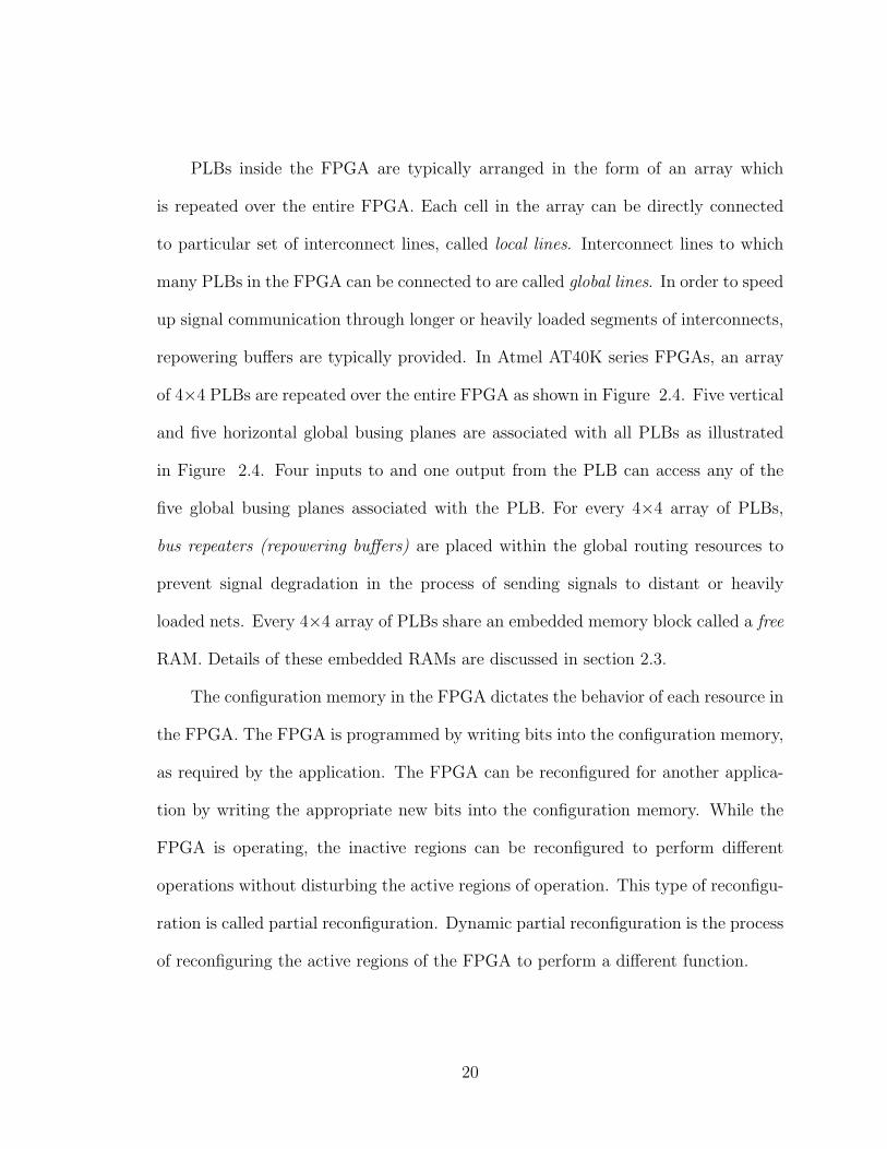
PLBs inside the FPGA are typically arranged in the form of an array which
is repeated over the entire FPGA. Each cell in the array can be directly connected
to particular set of interconnect lines, called local lines. Interconnect lines to which
many PLBs in the FPGA can be connected to are called global lines. In order to speed
up signal communication through longer or heavily loaded segments of interconnects,
repowering buffers are typically provided. In Atmel AT40K series FPGAs, an array
of 4×4 PLBs are repeated over the entire FPGA as shown in Figure 2.4. Five vertical
and five horizontal global busing planes are associated with all PLBs as illustrated
in Figure 2.4. Four inputs to and one output from the PLB can access any of the
five global busing planes associated with the PLB. For every 4×4 array of PLBs,
bus repeaters (repowering buffers) are placed within the global routing resources to
prevent signal degradation in the process of sending signals to distant or heavily
loaded nets. Every 4×4 array of PLBs share an embedded memory block called a free
RAM. Details of these embedded RAMs are discussed in section 2.3.
The configuration memory in the FPGA dictates the behavior of each resource in
the FPGA. The FPGA is programmed by writing bits into the configuration memory,
as required by the application. The FPGA can be reconfigured for another applica-
tion by writing the appropriate new bits into the configuration memory. While the
FPGA is operating, the inactive regions can be reconfigured to perform different
operations without disturbing the active regions of operation. This type of reconfigu-
ration is called partial reconfiguration. Dynamic partial reconfiguration is the process
of reconfiguring the active regions of the FPGA to perform a different function.
20

Cell
Hor
izon
tal B
usin
g P
lane
Vertical Busing Plane
I/O Pad
Free Ram
Logic Cell
RepeaterRow
RepeaterColumn
Figure 2.4: PLB Array Interconnection in Atmel AT40K Series FPGAs [29]
In general, only small portions of the logic circuitry are active at any given time.
By loading the logic functions into the FPGA as required, replacing or complementing
the logic already present, logic can be implemented efficiently. This concept is called
Cache Logic [30]. Thus cache logic operates similar to cache memory; active functions
are loaded into logic cache at any given time and unused functions or variations are
stored in low cost memory.
2.3 Embedded Memories
Memory is often integrated on the chip rather than off chip for significant reduc-
tion in cost and size. On-chip memory interface reduces capacitive load, power, heat
dissipation and helps in achieving higher speeds [31]. For similar reasons, memories
are embedded in both FPGAs and SoCs. SoCs typically contain different types of
memories like SRAMs, ROMs, DRAMs and flash memory blocks. FPGAs typically
21

contain heterogeneous memories, which can have different array sizes and depth. They
can also function in different modes like synchronous or asynchronous and single-port
or multi-port. Different kinds of memory technologies that exist are discussed in the
next subsection.
2.3.1 Memory Types
Memory cells can be designed in a number of ways. The structure of the memory
cells determines the type of memory chip. Figure 2.5 (a-c)shows the basic structures
of some memory cells. The memory cells shown are in the order of decreasing area and
decreasing speed. Figure 2.5 (d) shows a memory cell in a two-port memory block.
By adding more pass transistors and bit lines, a multi-port memory array can be
created. The type of memory embedded depends on the intended application of the
chip. SRAM technology is used for high speed applications. In applications requiring
large amounts of memory, DRAM technology is employed. While SRAM memories
are commonly embedded in FPGAs, a SoC can contain other kinds of memories. Most
of the FPGAs contain SRAM memories, as they are compatible with the process used
to fabricate logic on chip.
2.3.2 Embedded Memories in FPGAs
As shown in Figure 2.4, each 4×4 PLB array in the AT40K series FPGA shares
a memory block called a free RAM. These 32×4 dual-ported RAMs dispersed over
the entire array can be configured to operate in four different modes: single-port
22

Vdd
WordWord
BitBit
Read
WriteDin Dout
(a) Six-transistor SRAM cell (b) Three-transistor DRAM cell
Data
Read/write
(c) One-transistor DRAM cell
Wor
d1
Wor
d2
Bit2Bit1
Wor
d1
Wor
d2
Vdd
(d) Two-port memory cell
Bit2 Bit1
Figure 2.5: Structure of Memory Cells
synchronous, dual-port synchronous, single-port asynchronous and dual-port asyn-
chronous. All the RAMs except those in the rightmost column of the array can
operate in all four modes. RAMs in the rightmost column of the array can operate
only in single-port modes. Free RAMs are not true dual-port RAMs as they have
separate read and write ports instead of two ports that can be used for both reading
and writing [29]. A RAM in the leftmost column has its read address lines to its
right, while a RAM in the column adjacent to the right has its read address lines
to its left. This arrangement causes each RAM to share read address with one of
23

its adjacent RAMs and write address with the other as shown in Figure 2.6. This
arrangement provides easier memory to memory interconnect interfaces to increase
the width (number of bits used) and/or height (number of words) of the overall mem-
ory. When embedding memory into an FPGA, a good memory/logic interface is
critical [8] and so dedicated routing resources are provided for the data, address and
control signals of each free RAM.
AinDin Dout
OEN
WEN
Aout
Clk CLR
Din Dout
OEN
WEN
Ain
Clk CLR
AoutDin Dout
OEN
WEN
Ain
Clk CLR
Aout
Figure 2.6: Arrangement of Free RAMs in Atmel AT40K Series FPGAs
The architecture of a free RAM is as shown in Figure 2.7. In single-port mode,
the write address (Ain) lines are disconnected by opening the switch S1 and closing
switch S2 such that the read address (Aout) lines provide both the read address and
write address [29]. Data output (Dout) lines are disconnected by opening switch S4
and switch S3 is closed to read the data output from data input (Din) lines such that
the data bus is bidirectional. The tri-state buffer is enabled when output enable (OE)
is active low and data can be read out of the Din lines. In dual-port mode, switches
S1 and S4 are closed while switches S2 and S3 are opened. This enables two sets of
24

address lines and two sets of data lines for reading from and writing into the RAM
independently.
32 x 4 Dual-port free RAM
Read Address
Write Address
Write Enable
Data In Data Out
Clear
Load
Latch
Latch
Latch
Clock“1” “1”
5
5
4 4
“1” OE
RAM Clear
Ain
Aout
WEN
Din Dout
S2
S1
S3
S4
Figure 2.7: Architecture of a Free RAM Block [29]
As shown in Figure 2.7, latches are used for synchronizing the Write Address,
data and Write Enable. Reading of the RAM is always asynchronous. Both clock
multiplexers select the clock input in synchronous mode, and select logic ‘1’ in asyn-
chronous mode. The Load input is connected to each bit in the RAM. In synchronous
25
mode, the Clock input is connected to each bit in the RAM, while the Clock input
is inverted and is connected to the front-end latches. When the Load input is logic
‘1’, the latches are transparent. They latch the data when Load is logic ‘0’. Each bit
in the RAM is also a transparent latch. Thus the front-end memory latches and the
RAM form an edge-triggered flip-flop in synchronous mode and form a transparent
latch in asynchronous mode. A RAM-Clear Byte is used to clear the contents of the
RAMs during configuration [29].
There exist two different implementations of on-chip memory in FPGAs: fine-
grained and coarse-grained. In the fine-grained approach, each LUT can be configured
as RAM to implement large memories. In the coarse-grained approach, large memo-
ries are embedded inside the FPGA like the free RAMs in AT40K series FPGAs. This
approach results in denser memory implementation, but requires memory and logic
partitioning during FPGA design. Because of wide-varying memory requirements by
different applications, memory/logic partitioning might result in poor utilization of
either logic or memory. In order to avoid poor memory utilization, memory arrays
should be designed to be used for logic implementation if unused [9]. This is possi-
ble by configuring the memory as a ROM (by disabling write enable), allowing it to
function as a LUT for implementing large combinational logic. The on-chip memory,
block RAMs, in Virtex and Spartan series FPGAs, adopts this strategy.
Another important factor to be considered when embedding memory into an
FPGA is flexibility. Some applications might require a single large block of mem-
ory directly connected to logic, while some others might require smaller memories
26

connected to a common bus or smaller memories distributed over entire logic. There-
fore, embedded memories must be flexible enough to operate with different sizes and
widths. However, the more flexible the FPGA architecture is, the more programmable
switches and programming bits are required. Programmable switches might also add
delay to critical paths within a circuit implementation. In [32] it is shown that a
memory array containing between 512 and 2048 bits and which can be configured for
a word size of 1, 2, 4 or 8 can result in optimum flexibility, optimum logic and storage
implementation for many applications.
The block diagram of Virtex and Spartan II family FPGAs is as shown if Figure
2.8. PLBs are arranged in a 4×6 tile and repeated over the entire array. The array is
surrounded by IOBs. Large embedded block RAMs are present on either side of the
FPGA.
…….
…….
……
.
……
.
BLOCKRAM
BLOCK RAM
BLOCKRAM
BLOCKRAM
IOBs
PLBs PLBs
PLBs PLBs
Figure 2.8: Block Diagram of Spartan II Family FPGAs
27

Each PLB consists of two identical slices. A slice consists of two 4-input LUTs,
two storage elements, and carry logic. Each LUT can be configured as a 16×1-bit syn-
chronous RAM. Two LUTs in a slice can function as 16×2 or 32×1 synchronous RAMs
or a 16×1 dual-port synchronous RAM. Thus Virtex and Spartan II series FPGAs
adopt both fine grained and coarse grained approach for on-chip memory. Large
block RAMs complement small memory structures implemented in PLBs. These
block RAMs are 4 PLBs high and are present on either side of the chip.
Figure 2.9 shows the functional block diagram a block RAM where n = 12 and m
= 16 in Virtex and Spartan II FPGAs [33]. The block RAM is a true dual read/write
port fully synchronous RAM with 4K memory cells. Each port of the block RAM can
be independently configured as a read/write port, a read port or a write port, and
can be configured to a specific data width. Each port can independently access the
same 4096 locations and can be independently configured to have data widths of 1,
2, 4, 8 or 16 bits. The four control signals (CLK, WE, EN, RST) for each port have
independent inversion control as a configuration option [33].
2.3.3 Embedded Memories and FPGAs in SoCs and their Interfacing
Almost all SoCs contain some form of embedded memory and they typically
occupy about 70 % of total chip area [34]. Embedded SRAMs are widely used be-
cause, by merging with logic, data bandwidth can be increased and hardware cost
can be reduced. However, with pad limited, multi-million gate designs, other types
of embedded RAMs are also being used [35]. The following example illustrates uses
of other types of embedded RAMs.
28

Addr A
Din A
Addr B
Din B
Dout A
Dout B
n
m
n
m
m
m
WEAENARSTACLKA
WEBENBRSTBCLKB
Port A
Port B
Figure 2.9: Block Diagram of a Block RAM [33]
Figure 2.10 shows connections of the data SRAM embedded in Atmel’s AT94K
series SoC called the FPSLIC. Figure 2.11 shows the partitioning of the complete
embedded SRAM in Atmel’s FPLIC. This dual-ported SRAM is 36K bytes in size and
is shared by both FPGA and AVR (Advanced Virtual Reduced Instruction Set Com-
puter) microcontroller core. The embedded SRAM is partitioned into data SRAM
and program SRAM. While program SRAM is accessible only from the AVR core, the
data SRAM is accessible from both AVR core and FPGA core. The memory block
consists of 20 Kbytes of fixed program SRAM and 4 Kbytes of fixed data SRAM.
The remaining 12 Kbytes of memory are partitioned into three 4Kx8-bit blocks and
these blocks can be configured to be used as program SRAM or as data SRAM.
The “SOFT BOOT BLOCK” at the top of program memory is used by the chip on
power-up. The lower portion of the data SRAM (96 bytes) is not shared between the
AVR and FPGA; the AVR uses it for CPU general working registers and for memory
29

Embedded FPGA CORE
DATA SRAM4K x 8
To16K x 8
Embedded AVR CORE
FPGA Address lines
AVR Data Address Bus
16 16
FPGA Write Enable
AVR Write Enable
AVR Read Enable
FPGA CLK
AVR CLK
8
8
Data Read
Data Write Data Read/Write
8
B Side A Side
Figure 2.10: Embedded SRAM in Atmel’s FPSLIC [29]
mapped I/O. Therefore, on the FPGA side those bytes are available for data that is
only needed by the FPGA [29].
All cores in an SoC are connected with one or more bus structures. Bus-based
designs are easy to manage primarily because on-chip busses provide a common in-
terface by which cores can be connected [31]. Because of the diversity of embedded
cores, a segmented bus architecture is generally used [36]. FPSLIC uses a bus-based
interconnection structure.
The interfacing between FPGA core, memory core and microprocessor core in
Atmel’s FPSLIC is shown in Figure 2.12. The dual-port data SRAM core resides
between the FPGA and AVR cores enabling data exchange between AVR and FPGA
cores. Access by either core is via a 16-bit address bus and 8-bit bidirectional data
bus associated with each port. The FPGA core can also be directly accessed by the
30

4K x 8
4K x 8
4K x 8
AVR Reg Space
AVR Memory Mapped I/OFPGA
Access Only
FIXED 4K x 8
OPTIONAL
2K x 16
2K x 16
2K x 16
FIXED 10K x 16
OPTIONAL
SOFT “BOOT BLOCK”
Program SRAM Memory
Data SRAM Memory
Figure 2.11: Partitioning of Embedded SRAM in Atmel’s FPSLIC
AVR core. An 8-bit bus interconnects the FPGA core and the AVR allowing inter-
active communication. Up to 16 decoded address lines available from AVR into the
FPGA interface directly into the FPGA global busing resources. Up to 16 interrupts
are available from the FPGA to the AVR. The AVR core can also write into the
configuration memory of the FPGA core such that the FPGA can be dynamically
reconfigured by the AVR during system operation, without re-downloading config-
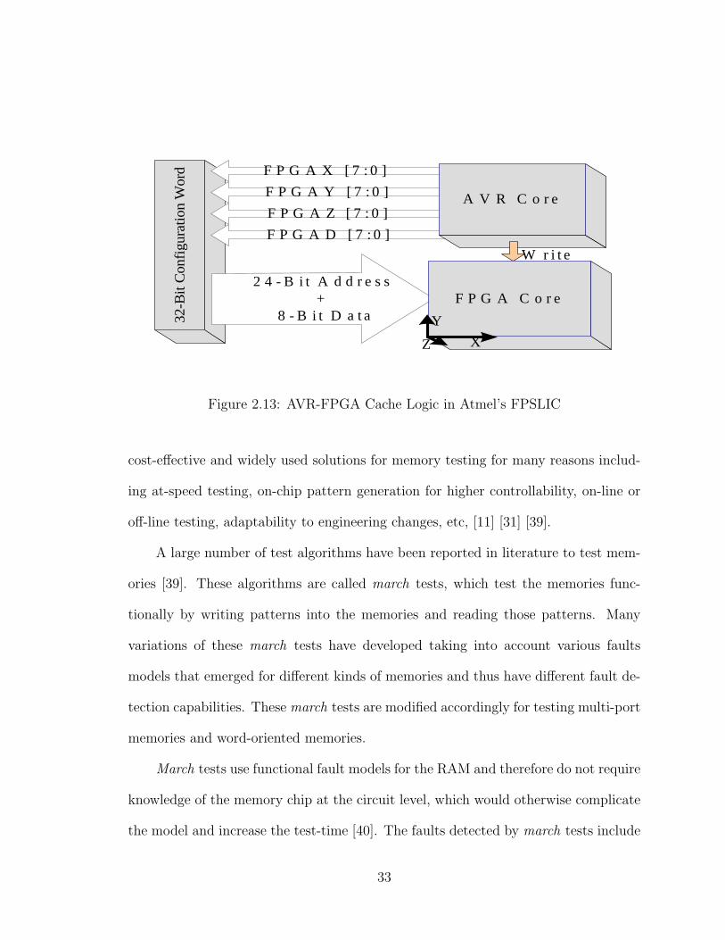
uration data externally. This access is illustrated in Figure 2.13, where FPGAX,
FPGAY, and FPGAZ specify the 24-bit address of the target configuration memory
byte of the FPGA to be reconfigured while FPGAD specifies the byte of configuration
data to be written into the configuration memory. The X and Y address values corre-
spond to the horizontal and vertical location of the PLB, RAM or routing resource to
be reconfigured. The Z address value corresponds to specific logic, RAM or routing
resources being configured.
31
D a ta S R A M
16-B
it A
ddre
ss B
us
16-B
it A
ddre
ss B
us
AV
R C
LK
8-B
it D
ata
Bus
Rea
d/W
rite
Enab
le
A V R C o r e
1 6 - B i t I n t e r r u p t B u s
1 6 - B i t I /O M e m o r y A d d r e s s B u s
8 - B i t D a t a B u s
R e a d /W r i t e E n a b l e
FPG
A C
LK
8-B
it D
ata
Bus
Rea
d/W
rite
Enab
le
F P G A C o r e
S o C
A s id e B s id e
Figure 2.12: AVR-FPGA-RAM Interface in Atmel’s FPSLIC
2.4 BIST for Memories
BIST was initially developed for random logic. Later, it was used to test ROMs,
RAMs and other structured logic. The regularity of these structures leads to more
efficient test generation and fault detection algorithms than for random logic [37].
Fault models used for memories are different from those used for digital logic. In ad-
dition to stuck-at, bridging and stuck-on/off faults, fault models like coupling faults,
pattern sensitive faults and address decoder faults are defined for memories. Because
of the modular nature of memory, BIST is suitable for testing both stand-alone mem-
ories and embedded memories [38]. BIST has been proven to be one of the most
32
32-B
it C
onfig
urat
ion
Wor
d
F P G A D [ 7 : 0 ]F P G A Z [ 7 : 0 ]F P G A Y [ 7 : 0 ]F P G A X [ 7 : 0 ]
A V R C o r e
2 4 - B i t A d d r e s s +
8 - B i t D a t aF P G A C o r e
XY
Z
W r i t e
Figure 2.13: AVR-FPGA Cache Logic in Atmel’s FPSLIC
cost-effective and widely used solutions for memory testing for many reasons includ-
ing at-speed testing, on-chip pattern generation for higher controllability, on-line or
off-line testing, adaptability to engineering changes, etc, [11] [31] [39].
A large number of test algorithms have been reported in literature to test mem-
ories [39]. These algorithms are called march tests, which test the memories func-
tionally by writing patterns into the memories and reading those patterns. Many
variations of these march tests have developed taking into account various faults
models that emerged for different kinds of memories and thus have different fault de-
tection capabilities. These march tests are modified accordingly for testing multi-port
memories and word-oriented memories.
March tests use functional fault models for the RAM and therefore do not require
knowledge of the memory chip at the circuit level, which would otherwise complicate
the model and increase the test-time [40]. The faults detected by march tests include
33
faults present in the address decoder, data line and refresh logic along with faults in
memory array cells. Typical faults covered by most of these tests include: Stuck-at
Faults (SAFs), Transition Faults (TFs), Coupling Faults (CFs) and Neighborhood
Pattern Sensitive Faults (NPSFs) [39]. The notation used for march tests is shown
below for the example of the March Y algorithm.
March Y test :m (w0);⇑ (r0, w1, r1);⇓ (r1, w0, r0);⇑ (r0);
The symbol ⇑ indicates RAM addressing in ascending order, the symbol ⇓ indi-
cates RAM addressing in descending order and the symbol m indicates RAM address-
ing in ascending or descending order. The notation w0 (w1) indicates writing all 0s
(writing all 1s). The notation r0 (r1) indicates reading all 0s (reading all 1s). March
tests are composed of march elements and these elements are separated by a semi-
colon. The length of a march Y test sequence is 8N, where N indicates the number
of words in the RAM, since the test sequence traverses the entire memory 8 times.
The march Y algorithm detects SAFs, TFs and address decoder faults but doesn’t
detect all CFs. Moreover, the use of all 0s and all 1s input patterns is not sufficient
to completely detect CFs and NPSFs. To ensure that pattern sensitive faults and
CFs (both inter-word and intra-word) are detected, modifications are made to the
march algorithms. The modifications consist of running the algorithm with Back-
ground Data Sequences (BDS) as described in [41]. For example, the BDS for a 4-bit
memory are: 0000(1111), 0101(1010) and 0011(1100). The number of BDS added is
equal to log2(K)+1, where the number of bits in a memory word is equal to 2K .
34

2.4.1 Present Methods for Testing FPGAs and SoCs
Different approaches exist in the literature for testing FPGAs [18] [19] [42] [43],
[44] [45]. In [44] an approach for testing PLBs of an FPGA is presented. An external
memory is used for storing test configurations and also test patterns. This approach
is dependent on the number of inputs and outputs of a PLB and also on the nature of
the PLB (combinational or sequential). Test configurations are developed after parti-
tioning PLBs into modules: a combinational module and a sequential module. PLBs
are connected to form one dimensional arrays and are tested in parallel. This ap-
proach was applied for testing PLBs in the Xilinx 4000 series FPGAs. This approach
needed 21 test phases and around 102 test vectors for completely testing the PLBs
including their RAM modes of operation [44]. Each time the FPGA is reconfigured
to test any resource, it is referred to as a test phase.
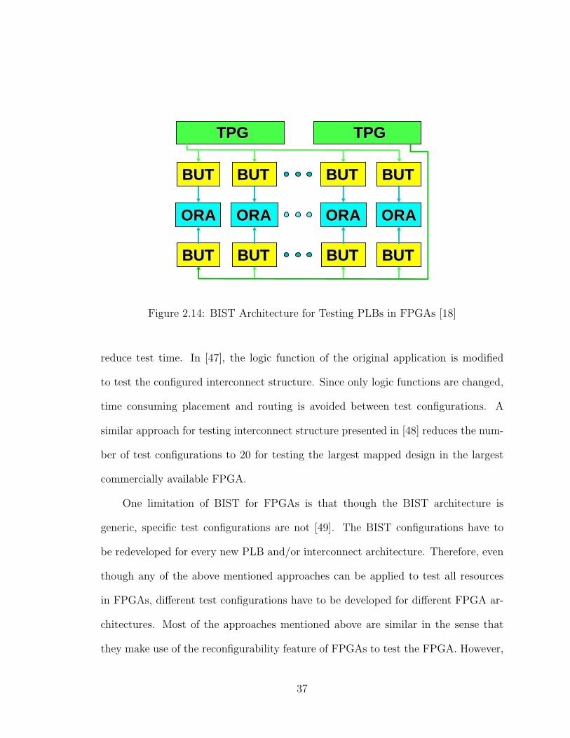
A BIST approach for testing PLBs in SRAM based FPGA was proposed in
[18]. In this approach, the BIST logic is created using the FPGA logic resources
during off-line testing, which takes advantage of the in-system reprogrammability
of the SRAM-based FPGAs and thus eliminating area overhead for BIST circuitry.
This BIST approach is applicable at all levels of testing (wafer, package, board and
system) and also provides at-speed testing [18]. Unlike the previous approach, the
Test Pattern Generator (TPG) is built inside the FPGA. This approach, however,
requires storage space for BIST configuration files. This approach involves using the
PLBs as TPGs, Blocks Under Test (BUTs) and Output Response Analyzers (ORAs)
as shown in the Figure 2.14. The functionality of the BUTs is changed during each
configuration until all the logic resources in the PLBs are tested. Each configuration
35

is downloaded into the FPGA and resulting ORA responses are obtained. Due to
penalties involved in storing expected responses, the ORA compares test responses
from two adjacent BUTs. For reliability reasons, each PLB is monitored by two
different ORAs and compared with two different BUTs. This approach yields correct
results as long as all the PLBs being compared do not contain functionally equivalent
faults. For completely testing PLBs and completely testing LUTs in RAM mode,
using the above mentioned approach, a total of 9 BIST configurations were required
for ORCA2C series FPGAs and 14 BIST configurations were required for ORCA2CA
series FPGAs [45]. A similar approach was adopted to test all logic resources in Xilinx
4000 and Spartan series FPGAs in [19]. LUTs that can be configured as RAMs in
Xilinx series FPGAs are tested in [19] using the approach described in [18]. For testing
all the logic resources including LUTs in RAM mode, a total of 12 configurations were
required for Xilinx 4000 and Spartan series FPGAs. A similar approach can be applied
for testing other resources, like embedded memories and interconnect, in the FPGAs
without any area overhead.
An approach to test the memory modules (LUTs in RAM mode) in SRAM-
based FPGAs is presented in [46]. The approach aims at reducing the number of test
configurations by taking into account the fact that the number of cells in memory
modules in a PLB is very small. A memory module with n inputs and 2 memory
modes (ROM and RAM) can be tested with 3n configurations and 8n ×2n test
patterns using this approach.
The concept of configuration-dependent testing was introduced in [47]. Configuration-
dependent testing involves determining that a particular configuration is fault free to
36
TTPPGG TTPPGG
BBUUTT
BBUUTT
OORRAA
BBUUTT
BBUUTT
OORRAA
BBUUTT
BBUUTT
OORRAA
BBUUTT
BBUUTT
OORRAA
Figure 2.14: BIST Architecture for Testing PLBs in FPGAs [18]
reduce test time. In [47], the logic function of the original application is modified
to test the configured interconnect structure. Since only logic functions are changed,
time consuming placement and routing is avoided between test configurations. A
similar approach for testing interconnect structure presented in [48] reduces the num-
ber of test configurations to 20 for testing the largest mapped design in the largest
commercially available FPGA.
One limitation of BIST for FPGAs is that though the BIST architecture is
generic, specific test configurations are not [49]. The BIST configurations have to
be redeveloped for every new PLB and/or interconnect architecture. Therefore, even
though any of the above mentioned approaches can be applied to test all resources
in FPGAs, different test configurations have to be developed for different FPGA ar-
chitectures. Most of the approaches mentioned above are similar in the sense that
they make use of the reconfigurability feature of FPGAs to test the FPGA. However,
37

each of these approaches aims at reducing the total number of test configurations so
that number of downloads can be reduced and with it the total test-time, since the
downloading process is the major component in FPGA test-time and cost.
2.5 Thesis Restatement
Existing methods for testing stand-alone FPGAs can also be applied for test-
ing FPGAs embedded in SoCs. However, utilization of some of the SOC features
(like accessibility of all cores by the embedded microcontroller) can help in devel-
oping a different test strategy that would reduce total test-time. Techniques used
to test embedded cores in FPGAs are described in [50] [51] [52] [53] [54]. Usage of
wrappers around memory and other cores for testing is described in [55]. In [54]
possible use of an embedded microcontroller core for testing all the accessible cores
in a SoC is discussed. This approach of using the microcontroller core for testing
other embedded cores forms the basis for one of the test techniques presented in this
thesis. Most of the current SoCs contain FPGA cores and memory cores. More-
over, the FPGA cores can be reconfigured at run-time by the microcontroller core,
which is generally the central core in a SoC. The microcontroller can be used to test
FPGA cores and dynamic reconfiguration feature can be used to reduce number of
downloads and hence the overall test-time. The implementation details and results
of this approach as applied for testing memory modules in Atmel’s AT94K SoC are
discussed in Chapter 3. Test development time can be reduced significantly if BIST
configurations developed are portable. VHDL can be used to develop portable code
for testing embedded memories in any FPGA. The other technique presented in this
38

thesis is development of portable code using VHDL for testing both embedded RAMs
and distributed RAMs in FPGAs. This approach uses the FPGA logic to test the
memory components. The details of this approach as applied to test memory cores
in Atmel’s AT40K FPGAs is presented in Chapter 3. Chapter 4 explains how this
approach is used to test embedded memories and other regular structure cores like
multipliers in Xilinx Spartan and Virtex FPGAs with minimal changes.
39

Chapter 3
Implementation Of BIST On ATMEL FPGAs And SoCs
The BIST approaches developed for testing RAMs in Atmel’s AT40K series
FPGAs and AT94K series SoCs are discussed in this chapter. The BIST architectures
and their implementation details are presented along with results from actual testing
of two different SoCs in the AT94K series. Finally, improvements to the performance
of BIST for RAMs in SoCs are also discussed.
3.1 RAM BIST Approaches
Two different approaches are followed for testing free RAMs in Atmel’s AT40K
series FPGAs and AT94K series FPSLIC. While the first approach is applicable for
both the devices, the second approach is only applicable for the FPSLIC. In the first
approach, all the BIST circuitry (TPG and ORAs) is built using FPGA logic re-
sources. This approach is suitable for testing RAMs in stand-alone FPGAs (which do
not have an embedded processor with partial reconfiguration capability) like AT40K
series FPGAs. In the second approach, TPG signals are generated by the embedded
microcontroller core (AVR) and the ORA is built using the FPGA logic. This ap-
proach is more suitable for testing embedded RAMs in SoCs and embedded FPGA(s)
where the FPGA can be accessed and can be partially reconfigured from an embed-
ded microcontroller core. This approach is, therefore, applicable only for the SoCs.
A mixture of these two approaches is used for testing data SRAM shared by both the
FPGA and the AVR in FPSLIC.
40

Free RAMs in AT94K and AT40K series FPGAs can be configured to operate as
single-port RAMs or dual-port RAMs in both synchronous and asynchronous modes
and have to be tested in all modes of operation. Only three modes are sufficient
to test free RAMs completely. The three modes are single-port synchronous mode,
single-port asynchronous mode and dual-port synchronous mode. Free RAMs are
not truly dual-ported and also the read-port is asynchronous. As a result, free RAMs
need not be tested in dual-port asynchronous mode. Also BDS are employed only in
single-port synchronous mode of testing. Coupling faults and neighborhood pattern
sensitive faults detected using BDS are memory specific and need not be detected
again.
3.1.1 BIST Approach for Free RAMs Using FPGA Logic
In this approach, the TPG which generates march sequences is built using FPGA
logic resources. The ORA, responsible for comparing output responses and storing
BIST results, is also built using FPGA logic resources. March algorithms used for
testing free RAMs and BIST architectures used in this approach are explained in the
following subsections.
3.1.1.1 BIST Architecture for Dual-port Synchronous Mode
The BIST architecture used for testing free RAMs in dual-port synchronous mode
is shown in Figure 3.1(a). All RAMs are tested in parallel using a single TPG and
the ORA is designed to compare outputs of two adjacent RAMs. All RAMs except
those on the rightmost and leftmost columns are compared by two ORAs. Two TPGs
41

are generally used for this kind of BIST architecture to make sure that TPG is not
faulty. But the Finite State Machine (FSM) based TPG is too large to replicate and
fit inside the device. Therefore, it is assumed that the logic and routing resources
are known to be fault-free as a result of previously executed BIST for programmable
logic and routing resources [56].
ORA
RAM
TPG
(a)
PLB PLB
Data from RAM1
Data from RAM2
Shift DataShift Control Clk Reset
Shift Data to Next ORA
(b)
Figure 3.1: a) Dual-Port Free RAM BIST Architecture b) ORA Design
The design of a single-bit ORA which uses two PLBs is shown in Figure 3.1(b).
The ORA latches a logic ‘1’ if any mismatch occurs at the RAM outputs during the
march sequence. All the ORAs are connected in the form of a scan chain to shift
42

the BIST results out. At the end of the BIST sequence, when the shift control pin is
high, the ORA acts as a shift register. Four single-bit ORAs are associated with each
RAM. In a N×N device, where N is the number of PLBs along one dimension of the
FPGA, there are (N /4)×((N /4)-1) dual-port RAMs, as the RAMs in the rightmost
column cannot act as dual-port RAMs. Since each bit in the left and right columns
of the dual-port RAMs is being compared by only one ORA, the number of PLBs
used for the ORA is equal to N×(N /4-2)/2.
The TPG generates a march sequence to supply RAM with data, address and
control signals. The DPR march algorithm used to test dual-port RAMs in [19] is
slightly modified and used to test dual-port free RAMs. The modified DPR march
sequence used is as follows:
DPRTest : m (w0 : n);⇓ (n : r0);⇑ (w1 :⇓ r1);⇓ (w0 :⇑ r0);
The notation used is as described in Chapter 2. Here, ‘n’ indicates no operation
on that particular port and the colon separates operations performed on the write
and read ports. The TPG is implemented as a FSM in VHDL and it synthesized to
66 PLBs. Four I/O pins are used: CLK input for running BIST and scanning results
out, RESET input for resetting the TPG and the ORA, SHIFT input for shifting
results out and SCANOUT data output for reading the results. The SHIFT pin also
goes to Shift Data input (as shown in Figure 3.1(b)) of the last ORA in the chain
and thus produces all 1s at the end of scan chain when shifting out the BIST results.
This provides a sanity check on the ORA data and assists in detecting certain faults
in the ORA scan chain [68]. The total number of clock cycles required for running the
43

BIST and retrieving the results is equal to 2112 + N×((N /4)-2), where N indicates
number of PLBs along one dimension of the array.
3.1.1.2 BIST Architecture for Single-port Modes
The BIST architecture for testing free RAMs in single-port synchronous and
asynchronous modes is similar and is as shown in Figure 3.2(a). All RAMs are
tested in parallel using a single TPG and the ORA compares data from RAMs with
expected read data results generated by the TPG. The design of the single-bit ORA is
shown in Figure 3.2(b). A tri-state buffer is required in this design as the write-data
lines are used for both reading and writing data in single-port mode. The active high
tri-state buffer in the ORA passes TPG data through when writing into the RAM and
is tri-stated when reading from the RAM which allows the read data to be compared
with expected data from the TPG. The tri-state buffer is controlled using the OEN
signal which also goes to the active low Output Enable signal of the RAM.
The ORA design for single-port mode, though not as simple as dual-port design,
makes diagnosis of RAMs much simpler. Such a design is not used in dual-port mode
because the generation of expected results by the TPG is more complicated as data
can be read and written at the same time and also routing resources are not sufficient
to implement such a design. For a N×N device, a total of N×N /2 PLBs are used
for the ORAs.
In synchronous single-port mode of operation, the March LR [57] algorithm is
used to test the free RAMs. The algorithm is modified by including BDS to test for
intra-word CFs and neighborhood pattern sensitive faults [41]. The length of the test
44

(a)
ORA
RAM
TPG
PLBShift Data
Shift Control Clk Reset
Shift Data to Next ORA
(b)
PLB
TPG Data
OEN
Data to/from RAM
Figure 3.2: a) Single-port Free RAM BIST Architecture b) ORA Design
sequence is 30×N, where N =32 for a free RAMs. The TPG is implemented in VHDL
and is synthesized to 123 PLBs. The sequence is as follows:
March LR test :m (w0000);⇓ (r0000;w1111);⇑ (r1111;w0000; r0000; r0000;
w1111);⇑ (r1111;w0000);⇑ (r0000;w1111; r1111; r1111;w0000);⇑ (r0000;w0101;
w1010; r1010);⇓ (r1010;w0101; r0101);⇑ (r0101;w0011;w1100; r1100);⇓ (r1100;
w0011; r0011);⇑ (r0011);
The same four I/O pins used in dual-port mode are used in single-port mode.
The total number of clock cycles required for running the BIST and retrieving the
45
results is equal to 960 + N×N /4, where N indicates number of PLBs along one
dimension of the array.
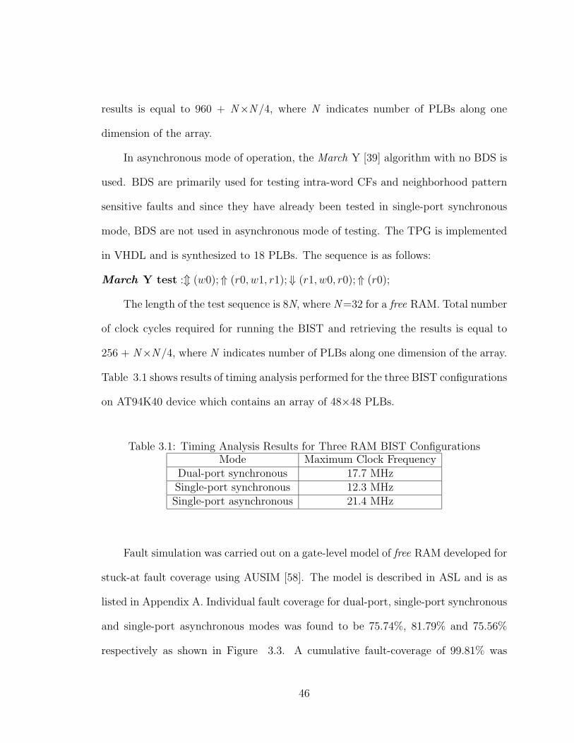
In asynchronous mode of operation, the March Y [39] algorithm with no BDS is
used. BDS are primarily used for testing intra-word CFs and neighborhood pattern
sensitive faults and since they have already been tested in single-port synchronous
mode, BDS are not used in asynchronous mode of testing. The TPG is implemented
in VHDL and is synthesized to 18 PLBs. The sequence is as follows:
March Y test :m (w0);⇑ (r0, w1, r1);⇓ (r1, w0, r0);⇑ (r0);
The length of the test sequence is 8N, where N =32 for a free RAM. Total number
of clock cycles required for running the BIST and retrieving the results is equal to
256 + N×N /4, where N indicates number of PLBs along one dimension of the array.
Table 3.1 shows results of timing analysis performed for the three BIST configurations
on AT94K40 device which contains an array of 48×48 PLBs.
Table 3.1: Timing Analysis Results for Three RAM BIST ConfigurationsMode Maximum Clock Frequency
Dual-port synchronous 17.7 MHzSingle-port synchronous 12.3 MHzSingle-port asynchronous 21.4 MHz
Fault simulation was carried out on a gate-level model of free RAM developed for
stuck-at fault coverage using AUSIM [58]. The model is described in ASL and is as
listed in Appendix A. Individual fault coverage for dual-port, single-port synchronous
and single-port asynchronous modes was found to be 75.74%, 81.79% and 75.56%
respectively as shown in Figure 3.3. A cumulative fault-coverage of 99.81% was
46

obtained for all three test configurations. A total of 1870 single stuck-at faults exist
in the model and 6 faults were found to be undetected.
0
20
40
60
80
100
1 2 3
RAM Configuration
Faul
t Cov
erag
e (%
)Individual FC Cumulative FC
DPSYNC
SPSYNC
SPASYNC
Figure 3.3: Fault Simulation Results for Free RAM
3.1.2 Advantages and Limitations of Using VHDL
Parameterized VHDL code is used to implement the BIST logic. This makes the
design portable and thus can be migrated onto other chips with minimal changes.
But for diagnosis of faults based on BIST results, some support is needed from the
synthesis tool. Unless the placement of RAMs with respect to the ORAs can be
controlled during synthesis, faulty RAMs cannot be identified from BIST results.
Placement cannot be controlled from Atmel’s synthesis tool (called Figaro) if VDHL
modeling is used. The solution is to either manually place the RAMs or maintain
47

mapping information for identifying physical locations of the faulty RAMs from BIST
results. As a design gets larger, manual placement becomes tedious. Also, the map-
ping information may change every time the design is synthesized. As a result, the
VHDL-only approach didn’t prove to be beneficial for Atmel’s FPGAs. A propri-
etary HDL is provided by Atmel for AT40K and AT94K devices. This language,
called Macro Generation Language (MGL) [59], has features similar to VHDL and
also has features that allow placement of logic blocks and define routing of intercon-
nect resources. As a result, a mixed approach is used by making use of both VHDL
and MGL. While MGL is used to define placement of RAMs and ORAs and their
interconnection, VHDL is used for the TPG. Since MGL does not support behavioral
description, designing the TPG with MGL implies transformation of the netlist into
MGL which would not be an easy task due to the complexity of the TPG. In order
to reduce development time, TPG is modeled using VHDL.
The fact that RAMs embedded in FPGAs can operate in different modes affects
the portability of VHDL. Furthermore, memories may have to be tested with dif-
ferent march sequences if memory technology changes. With the change in memory
technology, fault models adopted for testing may change and this results in redevel-
opment of VHDL code. To avoid this problem to some extent, a tool was created
which generates VHDL code automatically for a particular march sequence. This
tool, called RAMBISTGEN, generates VHDL code for any size of the memory and
for any active edge of the clock and any active levels for control signals. However, this
tool is currently capable of generating code for only single-port march sequences. A
snapshot of the tool is shown in Figure 3.4. This tool takes the input file containing
48

Figure 3.4: Snapshot of The RAMBISTGEN Tool
the march sequence and produces an output file containing the resulting VHDL code.
The format for the input file is as follows:
< u/d >< r/w >< data > [, < r/w >< data >].....
The above line represents the format for a march element of the sequence. Each
line starts with ‘u’ or ‘d ’ indicating the addressing order in up or down direction,
respectively. This is followed by ‘r ’ or ‘w ’ indicating read or write operation, re-
spectively. This is followed by the data to be read or written. Different read and
write operations are separated by a comma. Each line represents a different march
element. Address bus width is specified by the user in the GUI and data bus width is
interpreted from the read/write data in the input file. The format of the input files
for March Y and March LR algorithms is shown in Table 3.2.
49

Table 3.2: RAMBISTGEN Input File Format for March Y and March LRAlgorithm Input File Format
m (w0);⇑ (r0, w1, r1);⇓ (r1, w0, r0);⇑ (r0);
d w 0u r 0 , w 1, r 1d r 1, w 0 , r 0u r 0
m (w0000);⇓ (r0000;w1111);⇑ (r1111;w0000; r0000; r0000;w1111);⇑ (r1111;w0000);⇑ (r0000;w1111; r1111; r1111;w0000);⇑ (r0000;w0101;w1010; r1010);⇓ (r1010;w0101; r0101);⇑ (r0101;w0011;w1100; r1100);⇓ (r1100;w0011; r0011);⇑ (r0011);
u w 0000d r 0000 , w 1111u r 1111, w 0000, r 0000, r 0000, w 1111u r 1111, w 0000u r 0000, w 1111, r 1111, r 1111, w 0000u r 0000, w 0101, w 1010, r 1010d r 1010, w 0101, r 0101u r 0101, w 0011, w 1100 , r 1100d r 1100, w 0011, r 0011u r 0011
The input is not case sensitive. The tool generates approximately 140 and 300
lines of VHDL code for March Y and March LR algorithms, respectively. The tool
interprets the input file as follows:
1. Each line of the file is categorized as a phase.
2. All the words separated by a comma are treated as different elements of that phase.
For example, in u r 1111, w 0000 there are two elements: r 1111 and w 0000.
3. During FSM implementation, each phase is treated as a separate state and each
element of that phase forms a sub-state of that phase.
The resulting VHDL code for the above march sequences is given in Appendix
B. The tool was developed using Tool Control Language/Tool Kit (Tcl/Tk) and is
compatible with Windows and Linux environments. The line count for the source
code is 400.
50

3.1.3 BIST Approach for Free RAMs Using Embedded Processor Core
The idea of this approach is to generate TPG signals from the embedded proces-
sor core. As a result, this approach is applicable only to the FPSLIC. The processor
is also responsible for running the BIST, retrieving the BIST results, diagnosing the
results and reporting back the diagnostic results to a higher controlling device (PC for
example). The embedded processor in the FPSLIC can write into the configuration
memory of the FPGA. This capability of the processor is used in combining the three
RAM BIST configurations into one configuration. The free RAMs are initially config-
ured in dual-port synchronous mode for running BIST. Then RAMs and FPGA logic
are reconfigured to test RAMs in single-port synchronous and asynchronous modes.
Thus, by avoiding two of the three downloads, testing time can be reduced signifi-
cantly (approximately 3 times). Since only one bit-stream has to be stored instead of
three, memory requirements are also reduced by a factor of three. The TPG is very
irregular in structure. The rest of the circuit containing ORA and RAMs and can
be made regular. Thus, by making the BIST circuitry inside the FPGA regular, the
entire BIST logic to be built inside the FPGA (RAMs, ORAs and interconnections)
can be algorithmically configured by the processor. This further reduces testing time
because no bit-stream needs to be downloaded into the FPGA and requires just a
download into program memory of the AVR.
3.1.3.1 AVR-FPGA Interface Description
Before describing the actual implementation, the AVR-FPGA interface has to
be reviewed. The interface is illustrated in Figure 3.5. Data can be written into
51

the FPGA from the AVR through the AVR Data bus using any of the 16 IOSEL
lines. Whenever data is written into the AVR Data bus using one of the IOSELn
lines, the FPGAWE line and corresponding IOSELn line are asserted high for one
AVR clock cycle after stable data is produced on the AVR Data bus. Data can be
read from the FPGA through the AVR Data bus using any of the 16 IOSEL lines.
When reading data from the FPGA into the AVR Data bus, the FPGARE line and
corresponding IOSELn line is asserted high for one AVR clock cycle before stable
data is produced on the AVR Data bus. According to the FPLSIC datasheet [29], in
order to use IOSELn lines as a clock inside the FPGA, they have to be qualified with
the FPGAWE or the FPGARE line.
FPGA Side AVR Side
FPGA WE
FPGA RE
IOSEL0
IOSEL15
IOSEL1
8AVR Data
Figure 3.5: AVR-FPGA Interface
52

3.1.3.2 BIST Architecture
The architecture used is similar to the one used in the previous approach ex-
cept that the TPG signals are generated by the processor. In dual-port mode, as
in the previous approach, each ORA compares two adjacent RAMs as shown in Fig-
ure 3.6(a). In single-port mode, each ORA compares data from RAM with expected
data generated by the processor as shown in Figure 3.6(b).
ORA
RAM
Processor
TPG signals
ORA
RAM
Processor
(a) (b)TPG signals
Figure 3.6: Architecture of RAMBIST From AVR (a)Dual-port Mode (b) Single-portMode
3.1.3.3 Implementation of BIST Approach in FPSLIC
Initially free RAMs are configured to be tested in dual-port mode. The FPGAWE
and FPGARE lines are used as clocks for running BIST and for retrieving BIST
results, respectively. The AVR Data bus is used for providing address, data and
output enable signals to the free RAMs. Since the 8-bit wide data bus is not sufficient
to provide all required signals, all signals are registered as shown in Figure 3.7. The
53

IOSEL lines are used as enable signals for the registers. The function of each IOSELn
is shown in Table 3.3. IOSEL0 is used as global reset signal for clearing the ORAs.
The two registers are selected by IOSEL1 and IOSEL2 lines respectively. IOSEL3
line is used as clock enable for running BIST.
AVR
FPGA
Reg1
Reg2
ORA and RUTsTPG Data
Figure 3.7: RAMBIST Implementation from AVR
Table 3.3: Function of IOSEL LinesIOSEL Line Function
IOSEL0 ResetIOSEL1 Reg1 EnableIOSEL2 Reg2 EnableIOSEL3 BIST CLK Enable
As shown in Figure 3.7, two registers are used inside the FPGA for storing TPG
signals: an 8-bit wide register(Reg1) and a 5-bit wide register(Reg2). The contents
54
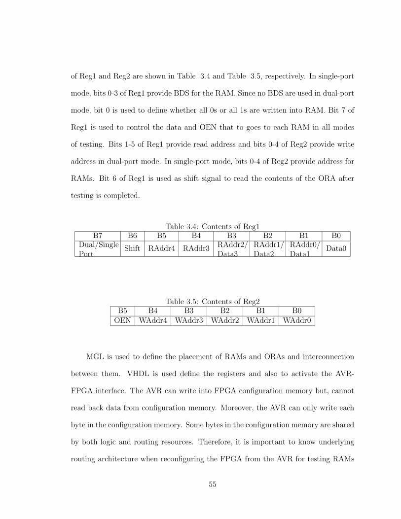
of Reg1 and Reg2 are shown in Table 3.4 and Table 3.5, respectively. In single-port
mode, bits 0-3 of Reg1 provide BDS for the RAM. Since no BDS are used in dual-port
mode, bit 0 is used to define whether all 0s or all 1s are written into RAM. Bit 7 of
Reg1 is used to control the data and OEN that to goes to each RAM in all modes
of testing. Bits 1-5 of Reg1 provide read address and bits 0-4 of Reg2 provide write
address in dual-port mode. In single-port mode, bits 0-4 of Reg2 provide address for
RAMs. Bit 6 of Reg1 is used as shift signal to read the contents of the ORA after
testing is completed.
Table 3.4: Contents of Reg1B7 B6 B5 B4 B3 B2 B1 B0
Dual/SinglePort
Shift RAddr4 RAddr3 RAddr2/Data3
RAddr1/Data2
RAddr0/Data1
Data0
Table 3.5: Contents of Reg2B5 B4 B3 B2 B1 B0
OEN WAddr4 WAddr3 WAddr2 WAddr1 WAddr0
MGL is used to define the placement of RAMs and ORAs and interconnection
between them. VHDL is used define the registers and also to activate the AVR-
FPGA interface. The AVR can write into FPGA configuration memory but, cannot
read back data from configuration memory. Moreover, the AVR can only write each
byte in the configuration memory. Some bytes in the configuration memory are shared
by both logic and routing resources. Therefore, it is important to know underlying
routing architecture when reconfiguring the FPGA from the AVR for testing RAMs
55

in a different mode. Therefore, MGL was used not only for placing RAMs and ORAs
but also for controlling the routing.
The program in the AVR memory for running the BIST is implemented in C lan-
guage. Once the program is downloaded, the AVR waits for a valid instruction from
a higher controlling device (PC in our case). AVR can be instructed to either run
BIST or to run diagnostics. If instructed to run BIST, AVR would return pass/fail
status to the PC after running BIST for a particular mode. If instructed to run diag-
nostics, AVR would return diagnostic results to the PC after executing the diagnostic
algorithm on the test results. A four-wire serial communication protocol is used for
communication between the PC and AVR.
3.1.4 On-Chip Diagnostics
AVR is not only capable of executing the BIST sequence and retrieving the
BIST results but also capable of performing diagnostic procedures based on the BIST
results for the identification of faulty RAMs in the FPGA core. The AVR, after
running diagnostic procedures, identifies the location of the faulty RAM in terms
of it’s X (column) and Y (row) coordinates. The AVR also identifies which bit(s)
of the RAM is faulty. Since two different BIST architectures are used for testing
free RAMs, two different diagnostic procedures were developed. In single-port test
configuration, the ORA compares the expected results generated by the AVR with
the data read from the RAMs Under Test (RUTs). Since the ORA incorporates
a shift register, the BIST results latched in the ORA are retrieved by the AVR.
Each bit retrieved corresponds to a single-bit of the 4-bit words of the RAM. The
56

position of the ORA in the FPGA array, and the corresponding RAM with which it is
associated, is determined by the ORA’s position in the shift register. As a result of the
ORA comparison of the RUTs output with the expected read results produced by the
TPG, the diagnostic procedure for the single-port RAM modes of operation is straight
forward. The diagnostic procedure looks for ORA failure indications (logic 1s) and
translates the positions based on the shift register order to identify not only which
RAMs are faulty but also which bits in a given RAM are faulty. A faulty ORA can
mimic a fault in its corresponding RAM. This can be identified when PLBs are tested.
In dual-port test configuration, since each ORA compares two adjacent RAMs
a different diagnostic approach is used. The Multiple Faulty Cell Locator (MULTI-
CELLO) algorithm originally developed for diagnosing faulty PLBs in FPGAs [45] is
used for diagnosis of dual-port RAMs. This procedure is more complicated because it
is possible that equivalent faults in two RAMs being compared by the same ORA will
go undetected. Since all the RAMs except those at the leftmost and the rightmost
edges of the FPGA are being observed by two sets of ORAs and being compared to
a different RAM in each set of ORAs, it is highly improbable for the faulty RAMs
to go undetected. This approach however loses diagnostic resolution for the RAMs
at the leftmost and rightmost edges of the FPGA. MULTICELLO algorithm marks
the faulty status of the RAMs to be unknown if the results indicate that there is any
possibility of faults. These ambiguities in the diagnosis can be overcome by rotating
the RAM BIST architecture by 90◦ such that rows of ORAs are comparing rows of
RAMs with the diagnostic procedure applied to the new BIST results. This procedure
of rotating and running the BIST has to be applied at the cost of increased testing
57
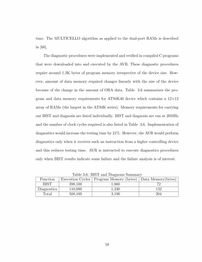
time. The MULTICELLO algorithm as applied to the dual-port RAMs is described
in [60].
The diagnostic procedures were implemented and verified in compiled C programs
that were downloaded into and executed by the AVR. These diagnostic procedures
require around 1.3K bytes of program memory irrespective of the device size. How-
ever, amount of data memory required changes linearly with the size of the device
because of the change in the amount of ORA data. Table 3.6 summarizes the pro-
gram and data memory requirements for AT94K40 device which contains a 12×12
array of RAMs (the largest in the AT94K series). Memory requirements for carrying
out BIST and diagnosis are listed individually. BIST and diagnosis are run at 20MHz
and the number of clock cycles required is also listed in Table 3.6. Implementation of
diagnostics would increase the testing time by 21%. However, the AVR would perform
diagnostics only when it receives such an instruction from a higher controlling device
and this reduces testing time. AVR is instructed to execute diagnostics procedures
only when BIST results indicate some failure and the failure analysis is of interest.
Table 3.6: BIST and Diagnosis SummaryFunction Execution Cycles Program Memory (bytes) Data Memory(bytes)
BIST 398,100 1,860 72Diagnostics 110,000 1,330 132
Total 508,100 3,190 204
58
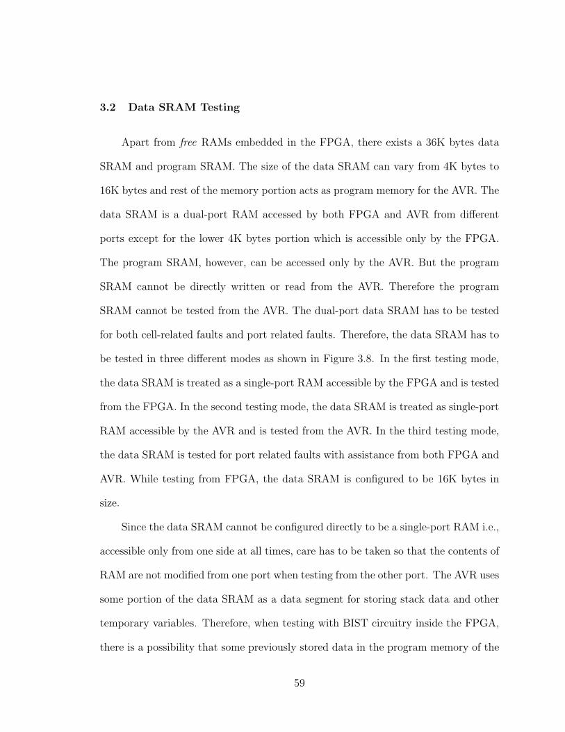
3.2 Data SRAM Testing
Apart from free RAMs embedded in the FPGA, there exists a 36K bytes data
SRAM and program SRAM. The size of the data SRAM can vary from 4K bytes to
16K bytes and rest of the memory portion acts as program memory for the AVR. The
data SRAM is a dual-port RAM accessed by both FPGA and AVR from different
ports except for the lower 4K bytes portion which is accessible only by the FPGA.
The program SRAM, however, can be accessed only by the AVR. But the program
SRAM cannot be directly written or read from the AVR. Therefore the program
SRAM cannot be tested from the AVR. The dual-port data SRAM has to be tested
for both cell-related faults and port related faults. Therefore, the data SRAM has to
be tested in three different modes as shown in Figure 3.8. In the first testing mode,
the data SRAM is treated as a single-port RAM accessible by the FPGA and is tested
from the FPGA. In the second testing mode, the data SRAM is treated as single-port
RAM accessible by the AVR and is tested from the AVR. In the third testing mode,
the data SRAM is tested for port related faults with assistance from both FPGA and
AVR. While testing from FPGA, the data SRAM is configured to be 16K bytes in
size.
Since the data SRAM cannot be configured directly to be a single-port RAM i.e.,
accessible only from one side at all times, care has to be taken so that the contents of
RAM are not modified from one port when testing from the other port. The AVR uses
some portion of the data SRAM as a data segment for storing stack data and other
temporary variables. Therefore, when testing with BIST circuitry inside the FPGA,
there is a possibility that some previously stored data in the program memory of the
59
AVR results in AVR stacking data in the data SRAM. To avoid failure results in such
a case, AVR has to be restricted from writing into the data SRAM. In first mode
of testing, this was achieved by having AVR execute an instruction which always
branches to the same location.
FPGA
data SRAM
AVR
data SRAM
AVR
data SRAM
FPGA
(a) (b) (c)
Figure 3.8: Three Configurations for Data SRAM testing (a) for Single-port Faultsfrom FPGA (b) for Single-port Faults from AVR (c) for Dual-port Faults from bothAVR and FPGA
The March LR with BDS is used to test data SRAM in the first mode of testing.
VHDL was used to implement March LR as a FSM and, when synthesized, 230 PLBs
are used for implementing the TPG in the FPGA and 16 PLBs are used for the ORA.
The ORA is configured as a scan chain for reading the BIST results. Diagnosis is
simple and is limited to indication of the faulty bit(s) of the RAM.
March LR with BDS is used for testing the 12K bytes portion of data SRAM
accessible from AVR. Since some portion of data SRAM is used by the AVR for
stacking data, two BIST configurations are required to completely test the data SRAM
60
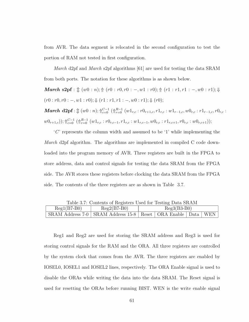
from AVR. The data segment is relocated in the second configuration to test the
portion of RAM not tested in first configuration.
March d2pf and March s2pf algorithms [61] are used for testing the data SRAM
from both ports. The notation for these algorithms is as shown below.
March s2pf : m (w0 : n);⇑ (r0 : r0, r0 : −, w1 : r0);⇑ (r1 : r1, r1 : −, w0 : r1);⇓
(r0 : r0, r0 : −, w1 : r0);⇓ (r1 : r1, r1 : −, w0 : r1);⇓ (r0);
March d2pf : m (w0 : n);⇑C−1c=0 (⇑R−1
r=0 (w1r,c : r0r+1,c, r1r,c : w1r−1,c, w0r,c : r1r−1,c, r0r,c :
w0r+1,c));⇑C−1c=0 (⇑R−1
r=0 (w1r,c : r0r,c−1, r1r,c : w1r,c−1, w0r,c : r1r,c+1, r0r,c : w0r,c+1));
‘C ’ represents the column width and assumed to be ‘1’ while implementing the
March d2pf algorithm. The algorithms are implemented in compiled C code down-
loaded into the program memory of AVR. Three registers are built in the FPGA to
store address, data and control signals for testing the data SRAM from the FPGA
side. The AVR stores these registers before clocking the data SRAM from the FPGA
side. The contents of the three registers are as shown in Table 3.7.
Table 3.7: Contents of Registers Used for Testing Data SRAMReg1(B7-B0) Reg2(B7-B0) Reg3(B3-B0)
SRAM Address 7-0 SRAM Address 15-8 Reset ORA Enable Data WEN
Reg1 and Reg2 are used for storing the SRAM address and Reg3 is used for
storing control signals for the RAM and the ORA. All three registers are controlled
by the system clock that comes from the AVR. The three registers are enabled by
IOSEL0, IOSEL1 and IOSEL2 lines, respectively. The ORA Enable signal is used to
disable the ORAs while writing the data into the data SRAM. The Reset signal is
used for resetting the ORAs before running BIST. WEN is the write enable signal
61

for the data SRAM. The Data bit of Reg3 indicates if data to be written into or
read from the data SRAM is either all 1’s or all 0’s. This data is compared by the
ORA with the data from the data SRAM during read operation. The ORA and the
data SRAM are clocked by the FPGAWE signal and IOSEL3 is used as clock enable
signal.
Because the AVR uses some portion of the data SRAM for stacking data, two
configurations are required to test the data SRAM in dual-port mode due to stack
relocation. A total of five configurations are required for completely testing the data
SRAM: three single-port tests and two dual-port tests. These five configurations are
reduced to three by combining two single-port tests with two dual-port tests. This
helps in reducing the testing time and also memory storage requirements.
3.3 Summary
Two approaches for testing the embedded memory cores were presented in this
chapter. The first approach aims at developing an FPGA independent BIST for em-
bedded memories. This is done by developing a parameterized VHDL code which
is portable and can used to test embedded memories in any FPGA with minimal
changes. However, for diagnosis, some support for placement control is needed from
the tools which synthesize the VHDL code. This approach was applied to test embed-
ded RAMs in Atmel’s FPGAs and SoCs. The portability of this approach is tested
by applying this approach to test embedded cores in Xilinx Virtex and Spartan series
FPGAs. The details of applying this approach to Xilinx devices and results of this
approach are discussed in Chapter 4.
62
The second approach aims at reducing the testing time. This approach, appli-
cable to SoCs, requires assistance from an embedded microcontroller. The partial
reconfiguration capability of the microcontroller can be used in combining different
BIST configurations. This avoids multiple downloads into the FPGA and reduces the
testing time significantly. Though this approach can be applied to other SoCs, some
development is required because of the changes in interfacing between microcontroller
and FPGA.
A summary of RAM BIST configurations and memory requirements for storing
BIST configurations are shown in Table 3.8 and Table 3.9 respectively. The single-
download method explained in this thesis improves both testing time and memory
requirements for storing BIST configurations by a factor of approximately 2.5 as
determined by running the tests on actual devices. As can be seen from Table 3.8,
by combining all configurations into one download, the download time decreases from
1500 ms to 600 ms. However, the time taken for running BIST and retrieving BIST
results increases from 311 us to 8.8 ms because concurrent execution inside the FPGA
is now replaced with sequential execution of AVR program code. This increase in
BIST running time ( 8.5ms) is very small compared to the decrease in download time
(900ms) and this results in significant improvement in total test-time.
All the above mentioned BIST configurations have been downloaded into Atmel
AT94K40 and AT94K10 SoCs and have been verified by injecting faults in various
resources of the FPGA.
Estimations of total test-time and memory storage requirements if the BIST
circuitry is algorithmically generated from the AVR without downloading into the
63

Table 3.8: Summary of RAM BIST Configurations for FPSLIC
Testingresource
Config
BISTexec.time(sec)
Dwldtime(ms)
Totaltesttime(ms)
TPGPLBs
ORAPLBs
MaxClkspeed(Hz)
Speed-
up
Free RAM Dual-port 147u 500 500.147 66 960 17.7M
testingSingle-portsync
124u 500 500.124 123 1152 12.3M 1
from FPGASingle-portasync
40u 500 500.04 18 1152 21.4M
Free RAMtestingfrom AVR
All modes 8.8m 600 608.8 14 1152 20M 2.46
Free RAMtestingwithoutdown-loadingintoFPGA
All modes 20m 180 200 14 1152 20M 7.5
Single-portfrom FPGA
32.7m 375 407.7 210 16 18.5M
Data SRAMSingle-port+dual-port
657m 375 1032 30 8 20M 1
Single-port+dual-portwith stackrelocation
95m 375 470 30 8 20M
FPGA are shown in bold in Table 3.8 and Table 3.9, respectively. Worst-case as-
sumptions for program size and partial reconfiguration time from the AVR result in
improvement of test-time by a factor of approximately 7.5 and improvement in mem-
ory requirements for storing BIST configurations by a factor of approximately 8 for
a 48×48(PLBs) device if a single compiled AVR code is downloaded. Generation of
BIST logic from AVR requires downloading compiled C code into program memory
64
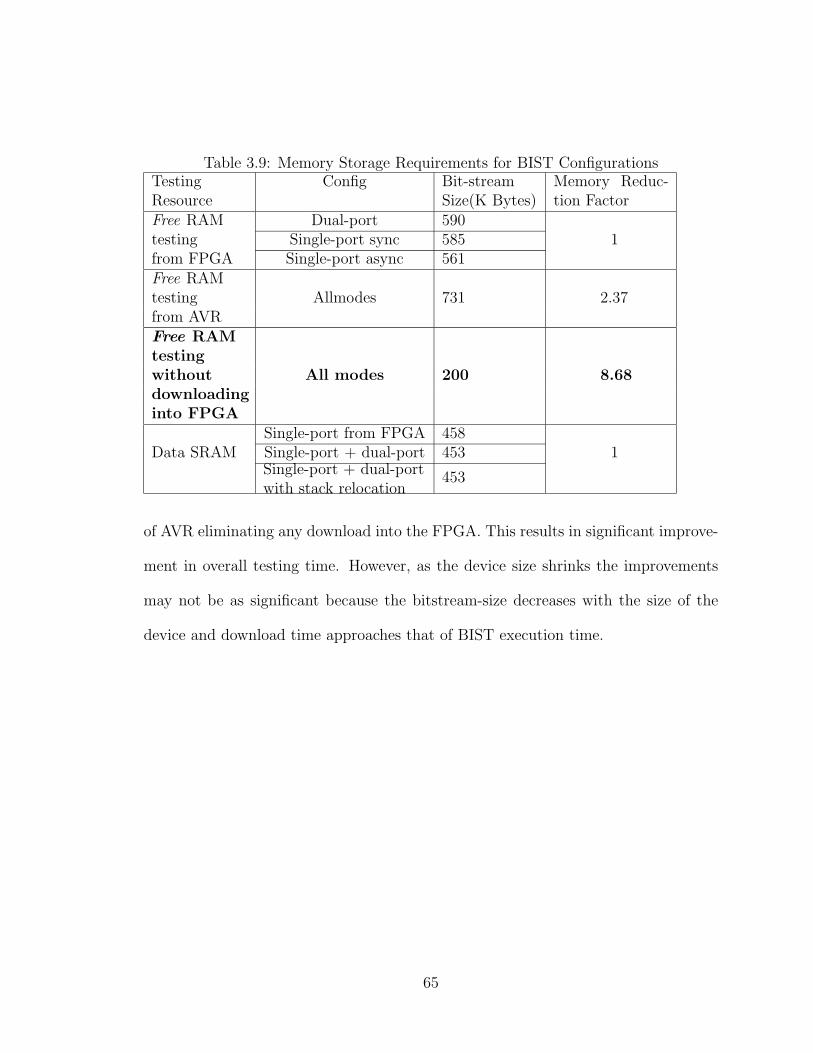
Table 3.9: Memory Storage Requirements for BIST ConfigurationsTestingResource
Config Bit-streamSize(K Bytes)
Memory Reduc-tion Factor
Free RAM Dual-port 590testing Single-port sync 585 1from FPGA Single-port async 561Free RAMtesting Allmodes 731 2.37from AVRFree RAMtestingwithout All modes 200 8.68downloadinginto FPGA
Data SRAMSingle-port from FPGA 458
1Single-port + dual-port 453Single-port + dual-portwith stack relocation
453
of AVR eliminating any download into the FPGA. This results in significant improve-
ment in overall testing time. However, as the device size shrinks the improvements
may not be as significant because the bitstream-size decreases with the size of the
device and download time approaches that of BIST execution time.
65
Chapter 4
Implementation of BIST on Xilinx FPGAs
BIST approaches for testing embedded block RAMs and distributed LUT RAMs
in Virtex and Spartan series FPGAs from Xilinx are discussed in this chapter. The
VHDL code originally developed for testing memory components in FPSLIC is used
for testing RAMs in Xilinx FPGAs with minimal changes. The impact of architectural
changes in Xilinx FPGAs on the BIST architecture and the changes needed in the
BIST implementation are also discussed.
4.1 Motivation
The basic BIST architecture used for PLBs in FPGAs is shown in Figure 2.14.
A similar BIST architecture is used for testing routing resources and memory com-
ponents in various families of FPGAs [19] [45] [60]. Though the BIST architecture is
independent of the FPGA, BIST configurations are architecture dependent and have
to be developed from scratch for different families of FPGAs. If BIST development for
one family of FPGAs can be reused, development time can be reduced significantly.
All FPGAs support logic implementation using a Hardware Description Language
(HDL) such as VHDL or Verilog. Since most HDLs are portable, BIST development
implemented for a given FPGA should be reusable in most of the other FPGAs. In
order to assess the flexibility and versatility of this approach, the VHDL-based BIST
developed for testing embedded RAMs in Atmel FPGAs is used for testing memory
components in Xilinx FPGAs. The architecture of Xilinx FPGAs is discussed in the
66

next section so as to compare with that of Atmel and discuss its impact on various
attributes of testing like total testing time, number of test configurations and the
BIST architecture.
4.2 PLB and Routing Architecture
Xilinx FPGAs adopt a coarse-grained architecture as opposed to the fine-grained
architecture adopted by the Atmel FPSLIC [62] [63] [64] [65] [66]. More logic can be
accommodated in a Xilinx PLB when compared to the Atmel PLB. PLBs in Spartan
and Virtex series FPGAs are made up of slices. Each slice typically contains two LUTs
and two storage elements along with other components. The basic architecture of a
slice is shown in Figure 4.1. Each slice in all the Xilinx FPGAs under consideration
for testing consists of two 4-input LUTs, two storage elements, fast carry look-ahead
chain and dedicated arithmetic logic gates. Multiplexers are used to handle larger
input logic functions by implementing Shannon’s expansion theorem. The LUTs can
also be configured to operate as a shift-register or a RAM, which form the distributed
memory in the FPGA. Each slice is capable of implementing a logic function of up
to 9 inputs [64].
Each PLB consists of two slices in Virtex I, Spartan II devices and four slices in
Spartan III, Virtex II and Virtex II Pro devices. Compared to Atmel PLBs, PLBs
in Xilinx devices are more complicated and capable of accommodating more logic.
Table 4.1 summarizes the minimum and maximum PLB array sizes of Xilinx family
FPGAs under consideration for testing.
67

LUT1
Shift Reg
RAM
LUT2
Shift Reg
RAM
Storage Element
Storage Element
Carry logic
Carry logic
Mux1
Mux2
Arithmetic Logic
Figure 4.1: Architecture of a Slice in Virtex and Spartan FPGAs [65]
The routing architecture of Xilinx devices is hierarchical and consists of long lines,
hex lines, double lines and local direct lines. Long lines span across the entire height
and width of the device [65] [64]. Hex lines connect to every third and sixth PLB away
in all four directions. Double lines connect to every first and second PLB away in all
four directions. PLBs access the above mentioned global routing resources through
a switch matrix. Local routing resources enable PLBs to connect to adjacent PLBs.
Local direct lines in Virtex and Spartan II FPGAs allow connections to horizontally
adjacent PLBs and in Virtex II and Virtex II Pro devices, direct lines can connect to
all surrounding 8 PLBs. Apart from these lines, there are internal lines to connect
LUTs in different slices of a given PLB [65] [64].
68

Table 4.1: PLB Array Size Bounds for Xilinx Family FPGAsFamily Min Size Max SizeVirtex I 16x24 64x96
Spartan II 8x12 28x42Spartan III 16x12 104x80Virtex II 8x8 112x104
Virtex II Pro 16x22 120x94
4.3 Embedded Block RAMs Architecture
In addition to the distributed memory of the LUT RAMs in PLBs, the Xilinx
FPGAs incorporate multiple large, dedicated RAMs called block RAMs [65] [64]. The
size of block RAMs varies with the device family. Block RAMs in Virtex I and Spartan
II are functionally identically identical and are 4K bits in size. They are arranged in
two columns at the rightmost and leftmost edges of the array and are 4 PLBs in height
as shown in Figure 4.2(a). Each block RAM contains two identical ports which can
be operated independently. They can be configured to operate in single-port mode
or in dual-port mode. Block RAMs are true dual-port RAMs, unlike free RAMs in
Atmel FPGAs. As a result, a different test algorithm has to be used. Block RAMs
are huge compared to free RAMs and this affects the testing time. Block RAMs in
Virtex I and Spartan II can operate in five different sizes (words x bits): 4096×1,
2048×2, 1024×4, 512×8, 256×16. This affects the number of configurations required
to completely test block RAMs, as will be discussed. Block RAMs can only operate
in synchronous modes.
Block RAMs in Virtex II, Spartan III and Virtex II Pro devices are functionally
identical and are 18K bits in size. However, the number of block RAMs and their
69

……
….
……
….
……
….
……
.
Block RAMs and multiplier blocks
……
.
PLBs
….
….
……
.
(a) (b) (c)
Figure 4.2: Organization of Block RAMs in (a) Virtex I and Spartan II FPGAs (b)Virtex II, Virtex II Pro and Spartan III FPGAs (c) Spartan III FPGAs
arrangement vary with the device in a particular family as shown in Figure 4.2(b) and
Figure 4.2(c). As a result, device characteristics have to be considered when placing
RAMs, as will be discussed. The 18K bits block RAMs operate in six different sizes
(words x size): 512×36, 1K×18, 2K×9, 4K×4, 8K×2 and 16K×1. For widths that are
not integral multiples of bytes, an additional parity bit is optionally provided for each
byte. All of these different modes of operation affect the number of configurations
required to completely test block RAMs, as will be discussed.
Three different write modes are provided in dual-port operation to maximize
throughput and efficiency of block RAMs [67]. The three modes are: WRITE FIRST,
READ FIRST and NO CHANGE. In WRITE FIRST mode, the input data is written
into the addressed RAM location and also simultaneously stored in the output data
latches and, if the other port tries to read the same location, the output data on
70

that port is unknown which means that the data can be either previously stored
data or data that is being currently written. In READ FIRST mode, data previously
present in the addressed RAM location is reflected on the output data lines while the
input data is being written into the addressed location and data previously stored is
reflected on the other port if it is trying to read the same location. In NO CHANGE
mode, the data on output data lines remain unchanged and, if the other port is trying
to read the same location, the output data on the port is unknown. The basic block
diagram of a block RAM is shown in Figure 4.3. Clock enable, set/reset, clock and
enable lines of each port can be independently configured to operate with any active
level(or edge in case of clock) as shown in Figure 4.3. Set/Reset signal, when asserted,
would initialize the data output latches synchronously to all 1s or all 0s. All these
features affect the number of BIST configurations and also the BIST architecture as
will be discussed.
4.4 Block RAM Testing
Block RAMs have to be tested in both single-port and dual-port modes. Initially,
the block RAM is configured in single-port mode to test for all cell-related faults.
Next, the block RAM is configured in dual-port mode to test for port related faults.
Since the block RAM can be configured to operate in different sizes, the block RAM
has to be tested in all possible sizes. For instance, since Virtex I and Spartan II devices
can operate in 5 different sizes, block RAMs are tested in single-port mode in all 5
sizes. BDS are used only with highest possible data width to detect the maximum
possible bridging faults among the data lines as well as CFs and NPSFs. BDS can
71

Enable
WENA
Set/ResetA
CLKA
EnableB
WENB
Set/ResetB
CLKB
Port A
Port B
AddessA [n-1 : 0]
AddessB [n-1 : 0]
DIA [m-1 : 0]
DIB [m-1 : 0]
DOA [m-1 : 0]
DOB [m-1 : 0]
Figure 4.3: Block Diagram of a Block RAM
be used in all configurations, but this would increase the total testing time apart
from increasing the complexity of the TPG. When testing in dual-port mode, block
RAMs are configured to operate with highest possible data width. One configuration
is sufficient since all the cell-related faults and configuration bits that set the data
width of the device have already been tested in single-port mode. The details of
the BIST architectures used and results of implementation are presented in the next
subsection.
72

4.4.1 Block RAM Testing in Single-port Mode
The BIST architecture used for testing block RAMs is as shown in Figure 4.4. A
single TPG is used for providing test patterns and control signals and the comparison
based-approach is used for the ORAs. The architecture is slightly modified from that
used for testing free RAMs which had less diagnostic resolution for the RAMs at the
edges. An extra column of ORAs are added to compare RAMs at the both edges.
This circular comparison was not possible for free RAMs due to limited logic and
routing resources.
TPG
ORA
RAM
Figure 4.4: BIST Architecture for Block RAMs Testing
Each port can be independently controlled to have different active levels for
write enable, set/reset, RAM enable and active clock edge signals as shown in Figure
4.3. Since five different configurations are required for completely testing single-
port modes, different active levels for control signals can be selected in different
configurations. Also WRITE FIRST, READ FIRST and NO CHANGE write-mode
73

options can also be selected during these five configurations. The reason for not
implementing expected data comparison as was done for Atmel free RAMs is to test
all write mode features in different configurations. Expected data generation requires
a separate TPG implementation for each of these write modes.
The Xilinx synthesis tool always selects port A when RAMs are configured in
single-port mode. In order to test both ports independently, block RAM is configured
as shown in Figure 4.5.
Port A
Port B
TPG
ENA
ENB
To ORA_A
To ORA_B
Set/Reset A
Set/Reset B
Figure 4.5: Block RAM Configuration for Testing both Ports in Single-port Mode
The block RAM is actually configured in dual-port mode and TPG provides
common test pattern signals for both ports except for RAM enable and set/reset
signals. Both the ports are enabled for only one clock cycle after BIST is started to
test the set/reset functionality of output latches. The TPG, which is implemented as
a state machine, enables only Port A during the first iteration of the march sequence
and enables Port B during the second iteration of the march sequence. Therefore,
74

except for one clock before the start of the first iteration, both ports are never enabled
at the same time and thus set/reset is never asserted high as shown in Figure 4.5.
The outputs from both the ports are compared with the data from identical ports of
two different RAMs by two different ORAs.
4.4.1.1 BIST Implementation
The entire BIST circuitry is designed using VHDL. The TPG is designed to
implement the March LR algorithm. BDS is used only when testing the RAM con-
figured to operate with largest possible data width. The TPG implemented in VHDL
is generated using RAMBISGEN tool. The algorithm used and its input file format
for generating VHDL code is listed in Appendix C.
The design of a single-bit ORA implemented in VHDL is as shown in Figure 4.6.
The design is identical to the one used for free RAMs in dual-port mode. One slice is
required to implement the single-bit ORA. A different ORA design can be used where
data from port A and data from port B can be compared as shown in Figure 4.8(a).
This reduces the number total number of ORAs required by a factor of 2 and can
be used in case of limited logic resources. However, the diagnostic resolution changes
from a single-port of a block RAM to a single block RAM.
The slice counts for implementing the TPG and the ORA for Virtex I and Spartan
II devices are shown in Table 4.2. PLB counts can be obtained by dividing the values
given in Table 4.2 by number of slices in the device. The total number of slices
required for implementing the BIST is greater than the sum of TPG slices and ORA
75

Data from RAM1
Data from RAM2
Slice
Shift DataShift Control Clk Reset
Shift Data to Next ORA
D Q
Figure 4.6: Design of a Single-bit ORA for Block RAM Testing
slices. This is because extra slices are required to buffer heavily loaded signals and
the number of extra slices required depends on the number of RAMs being tested.
Table 4.2: BIST PLB Count for Virtex I and Spartan IIFRAM BIST Algorithm TPG Slices ORA Slices
March LR w/o BDS 62March LR with BDS(16-bit) 110 N xDx2March LR with BDS(36-bit) 174
N = # of block RAMs, D = # of data bits
The Xilinx synthesis tool (ISE) allows placement of logic and RAMs to be con-
trolled via a constraint file and, hence, the VHDL-only approach was used for imple-
menting the BIST. The format for specifying the placement of RAMs is as follows:
LOC =RAMBn X# Y#.
X and Y represent the row and column coordinates of the RAM and the value
of n indicates the size of the memory and is device specific. For example, the INST
“RAM0” LOC = “RAMB16 X0 Y0” construct used in Virtex II and Virtex II Pro
76

FPGAs specifies that the placement tool places instance RAM0 of a 16K bits block
RAM at the bottommost left hand corner of the FPGA. The RAMB4 R# C# con-
struct is used in Virtex I and Spartan II FPGAs as the size of block RAMs is 4K bits
in these devices. Block RAM row and column designations are used instead of X and
Y coordinates in these devices.
The number of block RAMs and their arrangement varies with the device as
shown in Figure 4.2. In order to facilitate generation of the placement file for different
devices, a program to generate the constraint file is implemented in C language.
The same four BIST function I/O pins used for testing free RAMs are used for
testing block RAMs as shown in Table 4.3. In devices which have a JTAG interface
with access to the FPGA core, the boundary-scan interface can be used for download-
ing into FPGA configuration memory and also for running the BIST. The function of
Xilinx boundary-scan pins used as BIST I/O pins is shown in Table 4.3. The JTAG
interface allows defining the I/O interface for running BIST independent of the device
and package.
Table 4.3: Function of Xilinx JTAG pinsJTAG Pin FunctionDRCK1 ClkSEL2 ResetTDI Shift
TDO1 Scanout
77

4.4.1.2 Diagnosis
A modified version of the MULTICELLO algorithm, as explained in [68], is used
for performing diagnostics. This modified algorithm takes the circular comparison
of RAMs into account. Worst case scenarios wherein the modified MULTICELLO
algorithm is not able to find unique diagnosis is described in [69]. In order to obtain a
unique diagnosis in such cases, the pair-wise comparison of RAMs by the ORAs needs
to be changed by changing the location of the RAM in the constraint file. The code
has to be synthesized again to download and execute the new BIST configuration.
Then the diagnosis has to be reapplied taking the results of the previous diagnosis
into account.
4.4.2 Block RAM Testing in Dual-port Mode
The BIST architecture used is identical to the one used for single-port mode test-
ing of free RAMs shown in Figure 3.6. The TPG generates expected data assuming
that RAMs operate in write-first mode, which is the default mode. Since the different
write modes are tested in single-port mode, expected data comparison is feasible and
also diagnosis becomes simpler. The block RAMs are configured to operate with the
maximum data width and no BDS is used in this mode of testing. March s2pf and
March d2pf algorithms [61] used for testing data SRAM in FPSLIC are used for test-
ing block RAMs in dual-port mode. The two algorithms could be combined to form
a single configuration but this TPG becomes too large to fit in some smaller devices.
VHDL is used to implement the BIST and placement of RAMs is controlled
through a constraint file. The TPG and ORA slice counts are shown in Table 4.4.
78
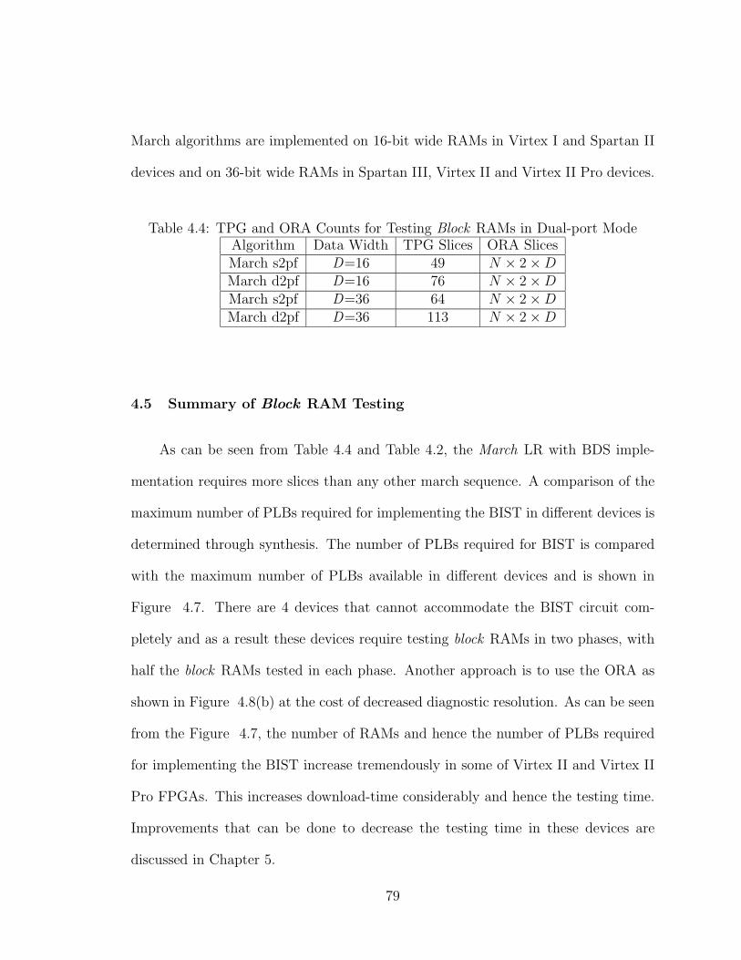
March algorithms are implemented on 16-bit wide RAMs in Virtex I and Spartan II
devices and on 36-bit wide RAMs in Spartan III, Virtex II and Virtex II Pro devices.
Table 4.4: TPG and ORA Counts for Testing Block RAMs in Dual-port ModeAlgorithm Data Width TPG Slices ORA SlicesMarch s2pf D=16 49 N × 2×DMarch d2pf D=16 76 N × 2×DMarch s2pf D=36 64 N × 2×DMarch d2pf D=36 113 N × 2×D
4.5 Summary of Block RAM Testing
As can be seen from Table 4.4 and Table 4.2, the March LR with BDS imple-
mentation requires more slices than any other march sequence. A comparison of the
maximum number of PLBs required for implementing the BIST in different devices is
determined through synthesis. The number of PLBs required for BIST is compared
with the maximum number of PLBs available in different devices and is shown in
Figure 4.7. There are 4 devices that cannot accommodate the BIST circuit com-
pletely and as a result these devices require testing block RAMs in two phases, with
half the block RAMs tested in each phase. Another approach is to use the ORA as
shown in Figure 4.8(b) at the cost of decreased diagnostic resolution. As can be seen
from the Figure 4.7, the number of RAMs and hence the number of PLBs required
for implementing the BIST increase tremendously in some of Virtex II and Virtex II
Pro FPGAs. This increases download-time considerably and hence the testing time.
Improvements that can be done to decrease the testing time in these devices are
discussed in Chapter 5.
79

All BIST configurations have been downloaded into Spartan II 2S50, Spartan II
2S200 and Virtex II Pro 2VP30 devices as shown in Figure 4.7 and were verified
using fault injection.
0
5
10
15
20
25
30
35
40
45
50
2S15
2S30
2S50
2S10
02S
150
2S20
0V
50V
100
V15
0V
200
V30
0V
400
V60
0V
800
V10
003S
503S
200
3S40
03S
1000
3S15
003S
2000
3S40
003S
5000
2V40
2V80
2V25
02V
500
2V10
002V
1500
2V20
002V
3000
2V40
002V
6000
2V80
002V
P2
2VP
42V
P7
2VP2
02V
PX
202V
P30
2VP4
02V
P50
2VP7
02V
PX
702V
P10
0
available in FPGAneeded for BIST
Slic
es (T
hous
ands
)
Devices with insufficient slices for BIST implementation
Devices used in this thesis
Figure 4.7: Programmable Logic Resources in Xilinx FPGAs
4.6 LUT RAM Testing
LUTs form distributed memory in Xilinx FPGAs. Each slice consists of two 4-
input LUTs (F-LUT and G-LUT), each of which can also function as a 16× 1 single-
port synchronous RAM. Both the LUTs in a slice can be combined to function as a
16× 2 single-port synchronous RAM, a 32× 1 single-port synchronous RAM or 16×
80

1 dual-port synchronous RAM. Theoretically, the maximum amount of distributed
memory is equal to 2× nslice × nplb × 16 bits, where nslice indicates number of slices
per PLB and nplb indicates number of PLBs in the device and a factor of 2 is due to
the fact that each slice consists of two LUTs.
Three configuration modes are required to completely test the LUT RAMs: 16×2
single-port mode, 32×1 single-port mode and 16×1 dual-port mode. All LUT RAMs
cannot be tested in parallel, as some LUTs are required for BIST logic (TPGs and
ORAs). Therefore, each of the three testing configurations requires two phases, where
the roles of the RUTs and the TPGs/ORAs are reversed in each phase.
4.6.1 BIST Implementation
The BIST architecture used in all three modes is identical to the one used for
PLBs as shown in Figure 2.14, with BUTs replaced by RUTs and two TPGs replaced
with a single TPG. The March Y algorithm used for testing asynchronous free RAMs
is used for testing in single-port modes and the DPR algorithm used for testing
free RAMs in dual-port mode is used for testing LUTs, as dual-port mode in the
LUT RAMs is not a true dual-port RAM. In fact the DPR algorithm was originally
developed for the LUT dual-port RAM mode in Xilinx FPGAs [19]. No BDS are
used in any of the modes. Comparison-based ORAs, as shown in Figure 4.8 (a), are
used for all three BIST configurations. Diagnostic resolution in all the configurations
is limited to a slice instead of a LUT RAM. The ORA design shown in Figure 4.8(b)
can also be used in any of the configurations since F and G LUTs are tested in parallel
81

RAM2 LUTG DataRAM1 LUT G Data
RAM2 LUTF DataRAM1 LUTF Data
Slice
Shift DataShift Control Clk Reset
Shift Data to Next ORA
D Q
Slice
Shift DataShift Control Clk Reset
Shift Data to Next ORA
D Q
RAM2 LUTG DataRAM1 LUT G Data
RAM2 LUTF DataRAM1 LUTF Data
(a)
(b)
Figure 4.8: ORA Designs Used for LUT RAM Testing
and the data that is read from these two LUTs is always identical. VHDL is used for
implementing the BIST and details of implementation are shown in Table 4.5.
All 3 LUT RAM BIST configurations have been downloaded into 2S50, 2S200
and V2P30 devices and verified using fault injection.
82
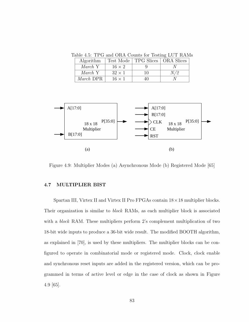
Table 4.5: TPG and ORA Counts for Testing LUT RAMsAlgorithm Test Mode TPG Slices ORA SlicesMarch Y 16× 2 9 NMarch Y 32× 1 10 N/2
March DPR 16× 1 40 N
18 x 18 Multiplier
A[17:0]B[17:0]
P[35:0]CLKCERST
18 x 18 Multiplier
A[17:0]
B[17:0]
P[35:0]
(a) (b)
Figure 4.9: Multiplier Modes (a) Asynchronous Mode (b) Registered Mode [65]
4.7 MULTIPLIER BIST
Spartan III, Virtex II and Virtex II Pro FPGAs contain 18×18 multiplier blocks.
Their organization is similar to block RAMs, as each multiplier block is associated
with a block RAM. These multipliers perform 2’s complement multiplication of two
18-bit wide inputs to produce a 36-bit wide result. The modified BOOTH algorithm,
as explained in [70], is used by these multipliers. The multiplier blocks can be con-
figured to operate in combinatorial mode or registered mode. Clock, clock enable
and synchronous reset inputs are added in the registered version, which can be pro-
grammed in terms of active level or edge in the case of clock as shown in Figure
4.9 [65].
83
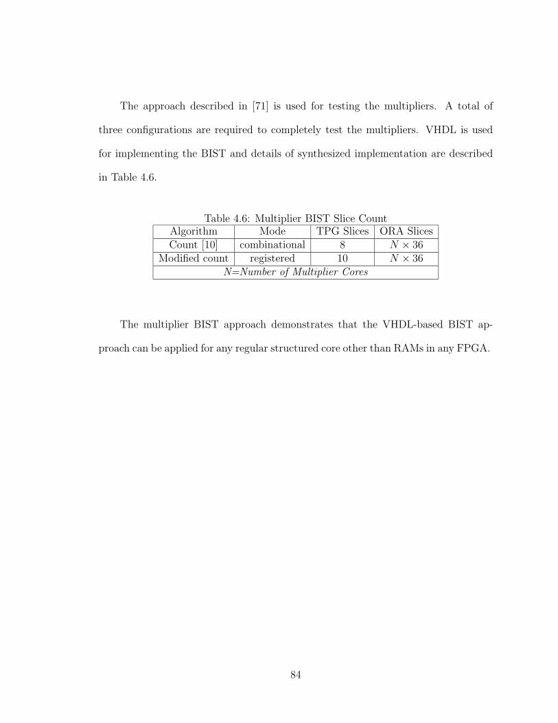
The approach described in [71] is used for testing the multipliers. A total of
three configurations are required to completely test the multipliers. VHDL is used
for implementing the BIST and details of synthesized implementation are described
in Table 4.6.
Table 4.6: Multiplier BIST Slice CountAlgorithm Mode TPG Slices ORA SlicesCount [10] combinational 8 N × 36
Modified count registered 10 N × 36N=Number of Multiplier Cores
The multiplier BIST approach demonstrates that the VHDL-based BIST ap-
proach can be applied for any regular structured core other than RAMs in any FPGA.
84

Chapter 5
Summary and Conclusions
BIST configurations for testing memory components in commercially available
FPGAs and SoCs are presented in this thesis. Two different approaches were followed
for developing BIST configurations to separately deal with two important features:
portability of BIST development and testing time. BIST configurations developed
were used to test memory components in AT40K series FPGAs and AT94K series
SoCs from Atmel and Spartan II, Spartan III, Virtex I, Virtex II series FPGAs and
Virtex II pro SoCs from Xilinx. A summary of the thesis, observations made during
BIST development, and suggestions for future research are discussed in this chapter.
5.1 Summary
The goal was to develop BIST configurations for testing free RAMs in AT40K
series FPGAs and AT94K series SOCs since they have embedded AT40K FPGA cores.
Initially VHDL was used to design the BIST circuitry. This approach was useful only
for pass/fail indication and not for diagnosis to indicate faulty RAMs due to lack of
support from the synthesis tool for control of placement of RAMs relative to their
associated ORAs. As a result, a combined VHDL-MGL approach was used to design
the BIST circuitry. Three BIST configurations were developed to completely test free
RAMs.
The embedded microcontroller (AVR) in AT94K series SoCs can access the em-
bedded FPGA core and can write into its configuration memory. This feature gave
85

rise to an alternate BIST approach for SoCs. The AVR was used to control the BIST
i.e., to start the BIST, retrieve the results after the BIST was completed and present
the results to a higher controlling device (PC) which performed diagnosis based on
BIST results. The same three BIST configurations were developed to test the free
RAMs from the AVR.
BIST circuitry implemented inside the FPGA can be made regular by moving
the irregular TPG function into the AVR, leaving only the ORAs and RAMs in the
FPGA. This gave rise to the possibility of combining the three BIST configurations
into one. This was possible because regular BIST structure inside the FPGA is similar
for all three configurations and can now easily be reconfigured by the AVR for the
next mode of testing. Diagnosis was also moved from PC to AVR and thus a single
configuration was developed which tests free RAMs completely and also performs
diagnosis.
A similar approach was used to test the embedded data SRAM shared by both
AVR and FPGA. Due to limitations imposed by the AVR architecture, three config-
urations were required to completely test the data SRAM.
The VHDL-only approach did not yield any benefits for Atmel FPGAs. However,
due to better synthesis tool support, the VHDL approach seemed worth experimenting
on Xilinx FPGAs. This approach yielded good results on Xilinx FPGAs by controlling
the placement of RAMs with respect to their associated ORAs. A portable VHDL
code was thus created to test embedded block RAMs and LUT RAMs in all families of
FPGAs from Xilinx. A total of 9 BIST configurations were developed for completely
testing block RAMs in all families of FPGAs from Xilinx. Another 3 configurations
86
were developed for testing LUT RAMs in all families of FPGAs from Xilinx. A
similar approach was used for testing embedded multipliers in some Xilinx FPGAs
and a total of 3 configurations were developed for testing them completely.
5.2 Observations
It was observed that the architecture of an FPGA has a significant impact on
BIST development. FPGAs using two different architectures were considered in this
thesis. Atmel FPGAs use fine-grained architecture as opposed to Xilinx FPGAs
which use coarse-grained architecture. In fine-grained FPGAs, it may not always
be possible to fit the entire BIST circuitry if synthesis tools are used for placement
and routing of entire design since heuristic algorithms used by FPGA synthesis tools
may not always come up with optimized placement and routing for the regular BIST
structure. This was noticed while developing BIST configurations for testing free
RAMs in single-port mode. Atmel’s design tool, called Figaro, could not fit the
entire design. This resulted in two configurations for completely testing free RAMs
in single-port synchronous mode, with half the RAMs tested in each configuration.
To avoid extra download, the placement and routing of the design was controlled
using MGL. Such a problem can occur with coarse-grained FPGAs as well when logic
or routing resources are used almost completely. Placement and routing problems
did not occur with Xilinx FPGAs when testing block RAMs. However, LUT RAM
testing caused placement and routing issues, as almost 100% of logic resources were
used. Routing issues were solved once placement of RUTs and ORAs were defined
with a constraint file.
87

TPG signals become heavily loaded, particularly when testing all the memory
components in a large FPGA with a single BIST configuration. The default fan-out
limit with the Xilinx synthesis tool is 15 and the tool will buffer the signals using
additional logic resources once the limit is exceeded. This prevented fitting the BIST
circuitry in some of the smaller FPGAs from Xilinx. This problem was solved by
increasing the user controlled fan-out limit to trade off speed of testing with number
of test configurations and thus the total testing time. Such a problem did not occur
with Atmel devices because the TPG signals are buffered as they pass through the
repeaters.
All Xilinx FPGAs support boundary-scan with facilities for access to the FPGA
core logic and this enabled usage of boundary-scan signals for downloading, running
and controlling the BIST. This provides a common interface for BIST independent of
the package being tested. Due to lack of access to the FPGA core by the boundary-
scan in Atmel devices, different I/O pins had to be used in different packages for
running BIST.
Atmel SoCs support writing into FPGA configuration memory but do not sup-
port reading of configuration memory or reading the contents of storage elements
in the device. As a result, ORAs were required to be configured as a scan chain to
shift out the results after running BIST. Read-back capability would save some testing
time and would also avoid the need for a scan chain. While the configuration memory
in Atmel devices is segmented into bytes, configuration memory in Xilinx FPGAs is
segmented into frames. The length of the frames varies with the device and typically
contains a few hundreds bits. Although Xilinx FPGAs have read-back capability, the
88
frame-level segmentation makes read-back complicated, as post processing of results
read back is required to extract the exact ORA data and, therefore, doesn’t reduce
testing significantly.
5.3 Future Research
To conclude the thesis, a few suggestions for improvements in the current BIST
approach and also some areas that can be explored are discussed.
Two kinds of approaches were used for output response analysis in this thesis:
comparison based approach and expected data comparison approach. It is better
to use the expected data comparison approach as the approach is more reliable and
makes diagnosis simpler as well. Comparison with adjacent elements detects all pos-
sible faults in the RAMs except for the case where all elements have equivalent faults
but fails to uniquely diagnose the results in cases where three or more adjacent el-
ements being compared have equivalent faults. Comparison with adjacent elements
was preferred over expected data comparison in some cases in this thesis as the latter
approach consumed more logic and routing resources and did not fit in some devices.
Virtex II Pro SoCs have embedded Power PC microprocessors similar to the
AVR in FPSLIC. The approach wherein the TPG was moved into the AVR and the
BIST was controlled by the AVR can be explored with Power PC in Virtex II Pro
SoCs. There is a possibility of this approach yielding more speed-up and memory
storage improvements in this device. Download time for the Virtex II Pro SoC is
much larger than that of FPSLIC because of larger configuration memory and also
the number of configurations for testing block RAMs is 9 as opposed to 3 for the free
89

RAMs in FPSLIC and these factors can result in better speed-up provided all block
RAM test configurations are combined into a single configuration executed by the
Power PC. The problem however is that the block RAMs form the program memory
for the Power PC.
With proper support from FPGA synthesis tools, the portable VHDL BIST
approach can also be experimented with logic blocks and routing in Xilinx FPGAs.
If a slice can be modeled using VHDL in such a way that the tool recognizes the model
as a slice, BIST development can be reduced significantly by following the approach
used for LUT RAM testing and logic BIST can be designed using VHDL alone and
by controlling the physical placement of logic blocks and ORAs.
90

Bibliography
[1] Arnaldo,B., “Systems on Chip: Evolutionary and Revolutionary Trends”, 3rdInternational Conference on Computer Architecture (ICCA’02), pp: 121-128,2002.
[2] J. Becker, “Configurable Systems-on-Chip (CSoC)”, Proc. IEEE Integrated Cir-cuits and Systems Design Symposium, pp: 379-384, 2002.
[3] M. Rabaey, “Experiences and Challenges in System Design”, Proc. IEEE Com-puter Society Workshop, pp: 2-4, 1998.
[4] J. Becker and M. Vorbach, “Architecture, Memory and Interface TechnologyIntegration of an Industrial/Academic Configurable System-on-Chip (CSoC)”,Proc. IEEE. Computer Society Annual Symposium, pp: 107-112, 2003.
[5] S. Knapp and D. Tavana, “Field Configurable System-On-Chip Device Architec-ture”, Proc. IEEE Custom Integrated Circuits Conference, pp: 155-158, 2000.
[6] K. Kawana, H. Keida, M. Sakamoto, K. Shibata and I.Moriyama, “An EfficientLogic Block Interconnect Architecture for User-Reprogrammable Gate Array”,Proc. IEEE Custom Integrated Circuits Conference, pp: 31.3/1-31.3/4, 1990.
[7] H. Verma, “Field Programmable Gate Arrays”, IEEE Potentials, Vol. 18, No.4, pp: 34-36, Oct - Nov, 1999.
[8] S.J.E Wilton, “Embedded Memory in FPGAs: Recent Research Results”, Proc.IEEE Pacific Rim Conference, pp: 292-296, 1999.
[9] S.J.E. Wilton, “Implementing Logic in FPGA Memory Arrays: HeterogeneousMemory Architectures”, Proc. IEEE Field-Programmable Technology, pp: 142-147, 2002.
[10] ,“International Technology Roadmap For Semiconductors (ITRS) 2000Update. Technical Report”, ITRS, 2000.
[11] V. Ratford, “Self-Repair Boosts Memory SoC Yields”, Integrated System De-sign, Sept 2001.
[12] A. Benso, S. Carlo, G. Natale, P. Prinetto, and M. Bodoni, “ProgrammableBuilt-in Self-Testing of Embedded RAM Clusters in System-on-Chip Architec-tures”, IEEE Communications Magazine, Vol. 41, No. 9, pp: 90-97, Sept 2003.
91
[13] B.G. Oomman, “A New Technology for System-on-Chip”, Electronics Engineer,April 2000.
[14] R. Chandramouli and S. Pateras, “Testing Systems on a Chip”, IEEE Spectrum,Vol. 33, No. 11, pp: 42-47, Nov 1996.
[15] V.D. Agrawal, R. Charles and K. Saluja, “A Tutorial on Built-in Self Test, Part1: Principles”, IEEE Design & Test of Computers, Vol. 10, No. 1, pp: 73-82,March 1993.
[16] H.J. Wunderlich, “Non-intrusive BIST for Systems-On-a-Chip”, Proc. IEEEInternational Test Conference, pp: 644-651, 2000.
[17] M. Abramovici , C.E. Stroud and M. Emmert, “Using Embedded FPGAs forSoC Yield Improvement”, Proc. Design Automation Conference, pp: 713-724,2002.
[18] C.E. Stroud, S. Konala, C. Ping and M. Abramovici, “Built-in Self-Test ofLogic Blocks in FPGAs (Finally, a Free Lunch: BIST Without Overhead!)”,Proc. VLSI Test Symposium, pp: 387- 392, 1996.
[19] C.E. Stroud, K.N. Leach, and T.A. Slaughter, “BIST for Xilinx 4000 and Spar-tan Series FPGAs: a Case Study”, Proc. IEEE International Test Conference,2003.
[20] S.M. Trimberger, “Field-Programmable Gate Array Technology”, Kluwer Pub-lishers, Norwell MA, 1994.
[21] G. Brebner, “Eccentric SoC Architectures as the Future Norm”, Proc. DigitalSystem Design, Euromicro Symposium, pp: 2-9,2003.
[22] S. Hauck, “The Roles of FPGA’s in Reprogrammable Systems” Proc. IEEE,Vol. 86, No. 4, pp: 615-638, April 1998.
[23] Y. Khalilollahi, “Switching Elements, the Key to FPGA Architecture”,WESCON Conference Record, pp: 682 - 687,1994.
[24] J. Rose, A. El Gamal and A. Sangiovanni-Vincentelli, “Architecture of Field-Programmable Gate Arrays”, Proc. IEEE, Vol. 81, No. 7, pp: 1013-1029, July1993.
[25] D.S. Brown, J.R. Francis, J. Rose and G.Z. Vranesic,“Field-Programmable Gate Arrays”, Kluwer Publishers, Norwell, MA,1992.
92

[26] J.V. Oldfield and R.C. Dorf, “Field-Programmable Gate Arrays:Reconfigurable Logic for Rapid Prototyping and Implementation of DigitalSystems”, John Wiley & Sons, New York, 1995.
[27] J. Rose, R.J. Francis, D. Lewis, and P. Chow, “Architecture of Field Pro-grammable Gate Arrays: The Effect of Logic Block Functionality on Area Ef-ficiency”, IEEE Journal of Solid-State Circuits, Vol. 25, No. 5, pp: 1217-1225,Oct 1990.
[28] , ”AT40K Series Field Programmable Gate Array”, Data Sheet, AtmelCorporation, 2003.
[29] , ”AT94K Series Field Programmable System Level Integrated Circuit”,Data Sheet, Atmel Corporation, 2003.
[30] R. Camarota and J. Rosenberg, “Cache Logic FPGAs for Building AdaptiveHardware”, FPGAs Technology and Applications, IEE Colloquium, pp: 1-3,1993.
[31] R. Rajsuman, “System-on-a-Chip: Design and Test”, Artech House, London,2000.
[32] S.J.E. Wilton, “Implementing Logic in FPGA Embedded Memory Arrays: Ar-chitectural Implications”, Proc. IEEE Custom Integrated Circuits Conference,pp: 269-272, 1998.
[33] Xilinx Corp., www.xilinx.com/products.
[34] S. Singh, S. Azmi, N. Agrawal, P. Phani, and A. Rout, “Architecture and De-sign of a High Performance SRAM for SOC Design”, Proc. Design AutomationConference, pp: 447-451, 2002.
[35] C.T. Huang, J.R Huang, C.F. Wu, C.W. Wu, and T.Y. Chang, “A Pro-grammable BIST Core for Embedded DRAM”, IEEE Design & Test of Com-puters, Vol. 16, No. 1, pp: 59-70, Jan - March 1999.
[36] T. Seceleanu, J. Plosila, and P. Lijeberg, “On-Chip Segmented Bus: a Self-Timed Approach”, Proc. IEEE, ASIC/SOC Conference, pp: 216-220, 2002.
[37] D. Bhatia, “Field Programmable Gate Arrays”, IEEE Potentials, Vol. 13, No.1, pp: 16-19, Feb 1994.
[38] E. Hall and G. Costakis, “Developing a Design Methodology for EmbeddedMemories”, Integrated System Design, January 2000.
93

[39] A.J. Van de Goor, “Testing Semiconductor Memories: Theory and Practice”,John Wiley & Sons, New York, 1991.
[40] A.J. Van de Goor, “An Overview of Deterministic Functional RAM Chip Test-ing”, ACM Computing Surveys, Vol. 22, No. 1, pp: 5-33, March 1990.
[41] A.J. Van de Goor, I. Tlili and S. Hamdioui, “Converting March Tests for Bit-Oriented Memories into Tests for Word-Oriented Memories,” Proc. IEEE In-ternational Workshop on Memory Technology Design and Testing, pp: 46-52,1998.
[42] M. Renovell and Y. Zorian, “Different Experiments in Test Generation for XilinxFPGAs”, Proc. International Test Conference, pp: 854-862, 2000.
[43] S.K. Lu, J.S. Shih and C.W. Wu, “Built-In Self-Test and Fault Diagnosis forLookup Table FPGAs”, Proc. IEEE Circuits and Systems, pp: 80-83, 2000.
[44] W.K. Huang, and F. Lombardi, “An Approach for Testing Programm-ble/Configurable Field Programmable Gate Arrays”, Proc. VLSI Test Sym-posium, pp: 450-455, 1996.
[45] C.E. Stroud, E. Lee, and M. Abramovici, ”BIST-Based Diagnostics of FPGALogic Blocks”, Proc. IEEE International Test Conference, pp: 539-547, 1997.
[46] W.K. Huang, F.J. Meyer, N. Park, and F. Lombardi, “Testing Memory Mod-ules in SRAM-Based Configurable FPGAs”, Proc. International Workshop onMemory Technology, Design and Testing, pp: 79-86, 1997.
[47] D. Das and N.A. Touba, “A Low Cost Approach for Detecting, Locating, andAvoiding Interconnect Faults in FPGA-Based Reconfigurable Systems”, Proc.International Conference on VLSI Design, pp: 266-269, 1999.
[48] M.B. Tahoori, “Application-Dependent Testing of FPGA Interconnects”, Proc.IEEE International Symposium on Defect and Fault Tolerance in VLSI Systems,pp: 409-416, 2003.
[49] C.E. Stroud, J. Nall, A. Taylor, M. Ford and L. Charnley, “A System for Auto-mated Generation of Built-In Self-Test for FPGAs”, Proc. International Con-ference on System Engineering, pp: 437-443, 2002.
[50] Y. Zorian , “System-Chip Test Strategies”, Proc. Design Automation Confer-ence, pp: 752-757, 1998.
[51] M.H. Tehranipour, S.M. Fakhraie, Z. Navabi and M.R. Movahedin, “A Low-Cost At-Speed BIST Architecture for Embedded Processor and SRAM Cores,”Journal of Electronic Testing: Theory and Applications, Vol. 20, No. 2, pp:155-168, April 2004.
94

[52] C. H. Tsai and C. Wu, “Processor-Programmable Memory BIST for Bus-Connected Embedded Memories”, Proc. Design Automation Conference, pp:325-330, 2001.
[53] A. Benso, S. Di Carlo, G. Di Natale, P. Prinetto and M. Lobetti Bodoni, “AProgrammable BIST Architecture for Clusters of Multiple-Port SRAMs”, Proc.IEEE International Test Conference, pp: 557-566, 2000.
[54] R. Rajsuman, “Testing a System-on-a-Chip with Embedded Microprocessor”,Proc. IEEE International Test Conference, pp: 499-508, 1999.
[55] F. Gharsalli, S. Meftali, F. Rousseau, and A.A. Jerraya, “Automatic Gener-ation of Embedded Memory Wrapper for Multiprocessor SoC”, Proc. DesignAutomation Conference, pp: 596-601, 2002.
[56] J.M. Harris, “Built-In Self Test Configurations for Field Programmable GateArrays Cores in Systems-on-Chip”, Masters Thesis, Auburn University, 2004.
[57] A. Van de Goor, G. Gaydadjiev, V.N. Jarmolik and V.G. Mikitjuk, “MarchLR: A Test for Realistic Linked Faults”, Proc. IEEE VLSI Test Symposium,pp: 272-280, 1996.
[58] C.E. Stroud, “AUSIM: Auburn University Simulator - Version L2.2”, Dept. ofElectrical & Computer Engineering, Auburn University, 2004.
[59] , ”Integrated Development System AT40K Macro Library Version 6.0”,Atmel Corporation, Oct. 1998.
[60] C.E. Stroud, S. Garimella and J. Sunwoo, “On-Chip BIST-Based Diagnosisof Embedded Programmable Logic Cores in System-on-Chip Devices”, Proc.International Conference on Computers and Their Applications,(pp: pending),2005.
[61] S. Hamdioui and A. Van de Goor, “Efficient Tests for Realistic Faults in Dual-Port SRAMs”, IEEE Transactions on Computers, Vol. 51, No. 5, pp: 460-473,May 2002.
[62] , “Virtex FPGAs”, Datasheet DS003, Xilinx Inc., 2004.
[63] , “Virtex II Platform FPGAs”, Datasheet DS031, Xilinx Inc., 2004.
[64] , “Spartan II Family FPGAs”, Datasheet DS001, Xilinx Inc., 2003.
[65] , “Virtex II Pro and Virtex II Pro X Platform FPGAs”, Datasheet DS083,Xilinx Inc., 2004.
95

[66] , “Spartan-3 FPGA Family”, Datasheet DS099, Xilinx Inc., 2004.
[67] , “Using Block RAM in Spartan-3 FPGAs”, Application note XAPP463,Xilinx Inc., 2003.
[68] M. Abramovici and C. Stroud, “BIST-Based Test and Diagnosis of FPGA LogicBlocks”, IEEE Trans. on VLSI Systems, Vol. 9, No. 1, pp: 159-172, Jan 2001.
[69] C. Stroud and S. Garimella, “Built-In Self-Test and Diagnosis of Multiple Em-bedded Cores in Generic SoCs”, to be published Proc. International Conferenceon Embedded Systems and Applications, 2005.
[70] O.L. Mac Sorley, “High speed arithmetic in binary computers”, Proc. IRE, Vol.49, No. 1, pp: 67-91, Jan 1961.
[71] D. Gizopoulos, A. Paschalis and Y. Zorian, “Effective Built-In Self-Test forBooth Multipliers”, IEEE Design & Test of Computers, Vol. 15, No. 3, pp:105-111, Sept 1998.
96

Appendices
97
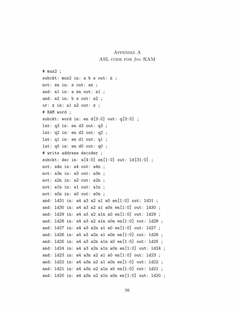
Appendix A
ASL code for free RAM
# mux2 ;
subckt: mux2 in: a b s out: z ;
not: sn in: s out: sn ;
and: a1 in: a sn out: a1 ;
and: a2 in: b s out: a2 ;
or: z in: a1 a2 out: z ;
# RAM word ;
subckt: word in: en d[3:0] out: q[3:0] ;
lat: q3 in: en d3 out: q3 ;
lat: q2 in: en d2 out: q2 ;
lat: q1 in: en d1 out: q1 ;
lat: q0 in: en d0 out: q0 ;
# write address decoder ;
subckt: dec in: a[4:0] en[1:0] out: ld[31:0] ;
not: a4n in: a4 out: a4n ;
not: a3n in: a3 out: a3n ;
not: a2n in: a2 out: a2n ;
not: a1n in: a1 out: a1n ;
not: a0n in: a0 out: a0n ;
and: ld31 in: a4 a3 a2 a1 a0 en[1:0] out: ld31 ;
and: ld30 in: a4 a3 a2 a1 a0n en[1:0] out: ld30 ;
and: ld29 in: a4 a3 a2 a1n a0 en[1:0] out: ld29 ;
and: ld28 in: a4 a3 a2 a1n a0n en[1:0] out: ld28 ;
and: ld27 in: a4 a3 a2n a1 a0 en[1:0] out: ld27 ;
and: ld26 in: a4 a3 a2n a1 a0n en[1:0] out: ld26 ;
and: ld25 in: a4 a3 a2n a1n a0 en[1:0] out: ld25 ;
and: ld24 in: a4 a3 a2n a1n a0n en[1:0] out: ld24 ;
and: ld23 in: a4 a3n a2 a1 a0 en[1:0] out: ld23 ;
and: ld22 in: a4 a3n a2 a1 a0n en[1:0] out: ld22 ;
and: ld21 in: a4 a3n a2 a1n a0 en[1:0] out: ld21 ;
and: ld20 in: a4 a3n a2 a1n a0n en[1:0] out: ld20 ;
98
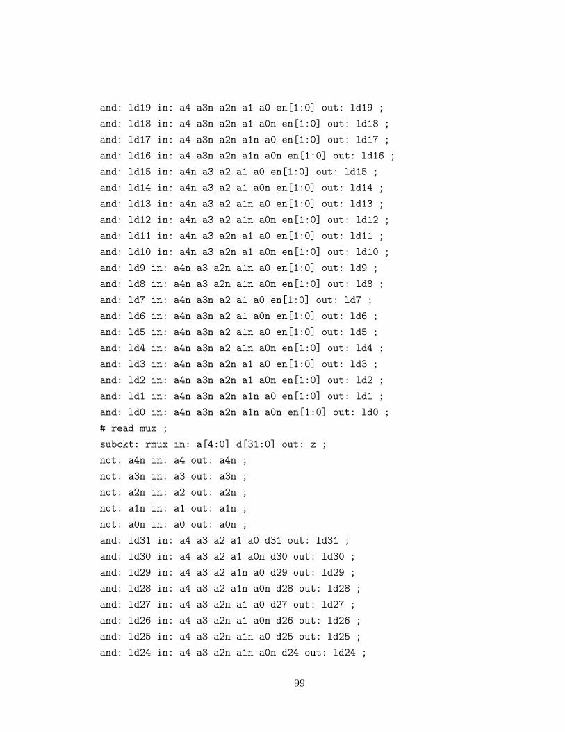
and: ld19 in: a4 a3n a2n a1 a0 en[1:0] out: ld19 ;
and: ld18 in: a4 a3n a2n a1 a0n en[1:0] out: ld18 ;
and: ld17 in: a4 a3n a2n a1n a0 en[1:0] out: ld17 ;
and: ld16 in: a4 a3n a2n a1n a0n en[1:0] out: ld16 ;
and: ld15 in: a4n a3 a2 a1 a0 en[1:0] out: ld15 ;
and: ld14 in: a4n a3 a2 a1 a0n en[1:0] out: ld14 ;
and: ld13 in: a4n a3 a2 a1n a0 en[1:0] out: ld13 ;
and: ld12 in: a4n a3 a2 a1n a0n en[1:0] out: ld12 ;
and: ld11 in: a4n a3 a2n a1 a0 en[1:0] out: ld11 ;
and: ld10 in: a4n a3 a2n a1 a0n en[1:0] out: ld10 ;
and: ld9 in: a4n a3 a2n a1n a0 en[1:0] out: ld9 ;
and: ld8 in: a4n a3 a2n a1n a0n en[1:0] out: ld8 ;
and: ld7 in: a4n a3n a2 a1 a0 en[1:0] out: ld7 ;
and: ld6 in: a4n a3n a2 a1 a0n en[1:0] out: ld6 ;
and: ld5 in: a4n a3n a2 a1n a0 en[1:0] out: ld5 ;
and: ld4 in: a4n a3n a2 a1n a0n en[1:0] out: ld4 ;
and: ld3 in: a4n a3n a2n a1 a0 en[1:0] out: ld3 ;
and: ld2 in: a4n a3n a2n a1 a0n en[1:0] out: ld2 ;
and: ld1 in: a4n a3n a2n a1n a0 en[1:0] out: ld1 ;
and: ld0 in: a4n a3n a2n a1n a0n en[1:0] out: ld0 ;
# read mux ;
subckt: rmux in: a[4:0] d[31:0] out: z ;
not: a4n in: a4 out: a4n ;
not: a3n in: a3 out: a3n ;
not: a2n in: a2 out: a2n ;
not: a1n in: a1 out: a1n ;
not: a0n in: a0 out: a0n ;
and: ld31 in: a4 a3 a2 a1 a0 d31 out: ld31 ;
and: ld30 in: a4 a3 a2 a1 a0n d30 out: ld30 ;
and: ld29 in: a4 a3 a2 a1n a0 d29 out: ld29 ;
and: ld28 in: a4 a3 a2 a1n a0n d28 out: ld28 ;
and: ld27 in: a4 a3 a2n a1 a0 d27 out: ld27 ;
and: ld26 in: a4 a3 a2n a1 a0n d26 out: ld26 ;
and: ld25 in: a4 a3 a2n a1n a0 d25 out: ld25 ;
and: ld24 in: a4 a3 a2n a1n a0n d24 out: ld24 ;
99

and: ld23 in: a4 a3n a2 a1 a0 d23 out: ld23 ;
and: ld22 in: a4 a3n a2 a1 a0n d22 out: ld22 ;
and: ld21 in: a4 a3n a2 a1n a0 d21 out: ld21 ;
and: ld20 in: a4 a3n a2 a1n a0n d20 out: ld20 ;
and: ld19 in: a4 a3n a2n a1 a0 d19 out: ld19 ;
and: ld18 in: a4 a3n a2n a1 a0n d18 out: ld18 ;
and: ld17 in: a4 a3n a2n a1n a0 d17 out: ld17 ;
and: ld16 in: a4 a3n a2n a1n a0n d16 out: ld16 ;
and: ld15 in: a4n a3 a2 a1 a0 d15 out: ld15 ;
and: ld14 in: a4n a3 a2 a1 a0n d14 out: ld14 ;
and: ld13 in: a4n a3 a2 a1n a0 d13 out: ld13 ;
and: ld12 in: a4n a3 a2 a1n a0n d12 out: ld12 ;
and: ld11 in: a4n a3 a2n a1 a0 d11 out: ld11 ;
and: ld10 in: a4n a3 a2n a1 a0n d10 out: ld10 ;
and: ld9 in: a4n a3 a2n a1n a0 d9 out: ld9 ;
and: ld8 in: a4n a3 a2n a1n a0n d8 out: ld8 ;
and: ld7 in: a4n a3n a2 a1 a0 d7 out: ld7 ;
and: ld6 in: a4n a3n a2 a1 a0n d6 out: ld6 ;
and: ld5 in: a4n a3n a2 a1n a0 d5 out: ld5 ;
and: ld4 in: a4n a3n a2 a1n a0n d4 out: ld4 ;
and: ld3 in: a4n a3n a2n a1 a0 d3 out: ld3 ;
and: ld2 in: a4n a3n a2n a1 a0n d2 out: ld2 ;
and: ld1 in: a4n a3n a2n a1n a0 d1 out: ld1 ;
and: ld0 in: a4n a3n a2n a1n a0n d0 out: ld0 ;
or: z in: ld[31:0] out: z ;
# complete RAM ;
ckt: fRAM
in: clk radd[4:0] wadd[4:0] wen di[3:0] oen
con: async dpr
out: dout[3:0] ;
# config bits (async=1 => asynchronous) (dpr=1 => dualport) ;
# RAM core ;
word: w0 in: ld0 din[3:0] out: w0d[3:0] ;
word: w1 in: ld1 din[3:0] out: w1d[3:0] ;
word: w2 in: ld2 din[3:0] out: w2d[3:0] ;
100

word: w3 in: ld3 din[3:0] out: w3d[3:0] ;
word: w4 in: ld4 din[3:0] out: w4d[3:0] ;
word: w5 in: ld5 din[3:0] out: w5d[3:0] ;
word: w6 in: ld6 din[3:0] out: w6d[3:0] ;
word: w7 in: ld7 din[3:0] out: w7d[3:0] ;
word: w8 in: ld8 din[3:0] out: w8d[3:0] ;
word: w9 in: ld9 din[3:0] out: w9d[3:0] ;
word: w10 in: ld10 din[3:0] out: w10d[3:0] ;
word: w11 in: ld11 din[3:0] out: w11d[3:0] ;
word: w12 in: ld12 din[3:0] out: w12d[3:0] ;
word: w13 in: ld13 din[3:0] out: w13d[3:0] ;
word: w14 in: ld14 din[3:0] out: w14d[3:0] ;
word: w15 in: ld15 din[3:0] out: w15d[3:0] ;
word: w16 in: ld16 din[3:0] out: w16d[3:0] ;
word: w17 in: ld17 din[3:0] out: w17d[3:0] ;
word: w18 in: ld18 din[3:0] out: w18d[3:0] ;
word: w19 in: ld19 din[3:0] out: w19d[3:0] ;
word: w20 in: ld20 din[3:0] out: w20d[3:0] ;
word: w21 in: ld21 din[3:0] out: w21d[3:0] ;
word: w22 in: ld22 din[3:0] out: w22d[3:0] ;
word: w23 in: ld23 din[3:0] out: w23d[3:0] ;
word: w24 in: ld24 din[3:0] out: w24d[3:0] ;
word: w25 in: ld25 din[3:0] out: w25d[3:0] ;
word: w26 in: ld26 din[3:0] out: w26d[3:0] ;
word: w27 in: ld27 din[3:0] out: w27d[3:0] ;
word: w28 in: ld28 din[3:0] out: w28d[3:0] ;
word: w29 in: ld29 din[3:0] out: w29d[3:0] ;
word: w30 in: ld30 din[3:0] out: w30d[3:0] ;
word: w31 in: ld31 din[3:0] out: w31d[3:0] ;
# input latches ;
not: we in: wen out: we ;
lat: wr in: men we out: wr ;
lat: wa0 in: men wadd0 out: wa0 ;
lat: wa1 in: men wadd1 out: wa1 ;
lat: wa2 in: men wadd2 out: wa2 ;
101
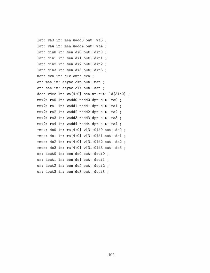
lat: wa3 in: men wadd3 out: wa3 ;
lat: wa4 in: men wadd4 out: wa4 ;
lat: din0 in: men di0 out: din0 ;
lat: din1 in: men di1 out: din1 ;
lat: din2 in: men di2 out: din2 ;
lat: din3 in: men di3 out: din3 ;
not: ckn in: clk out: ckn ;
or: men in: async ckn out: men ;
or: sen in: async clk out: sen ;
dec: wdec in: wa[4:0] sen wr out: ld[31:0] ;
mux2: ra0 in: wadd0 radd0 dpr out: ra0 ;
mux2: ra1 in: wadd1 radd1 dpr out: ra1 ;
mux2: ra2 in: wadd2 radd2 dpr out: ra2 ;
mux2: ra3 in: wadd3 radd3 dpr out: ra3 ;
mux2: ra4 in: wadd4 radd4 dpr out: ra4 ;
rmux: do0 in: ra[4:0] w[31:0]d0 out: do0 ;
rmux: do1 in: ra[4:0] w[31:0]d1 out: do1 ;
rmux: do2 in: ra[4:0] w[31:0]d2 out: do2 ;
rmux: do3 in: ra[4:0] w[31:0]d3 out: do3 ;
or: dout0 in: oen do0 out: dout0 ;
or: dout1 in: oen do1 out: dout1 ;
or: dout2 in: oen do2 out: dout2 ;
or: dout3 in: oen do3 out: dout3 ;
102
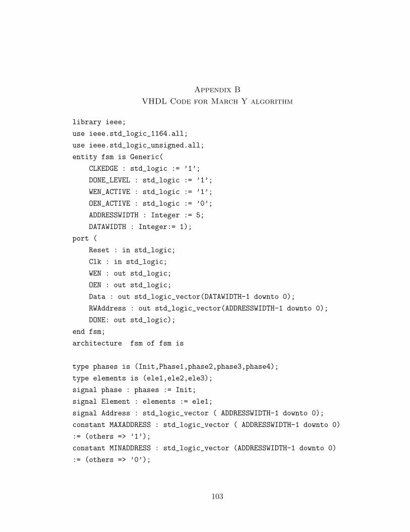
Appendix B
VHDL Code for March Y algorithm
library ieee;
use ieee.std_logic_1164.all;
use ieee.std_logic_unsigned.all;
entity fsm is Generic(
CLKEDGE : std_logic := ’1’;
DONE_LEVEL : std_logic := ’1’;
WEN_ACTIVE : std_logic := ’1’;
OEN_ACTIVE : std_logic := ’0’;
ADDRESSWIDTH : Integer := 5;
DATAWIDTH : Integer:= 1);
port (
Reset : in std_logic;
Clk : in std_logic;
WEN : out std_logic;
OEN : out std_logic;
Data : out std_logic_vector(DATAWIDTH-1 downto 0);
RWAddress : out std_logic_vector(ADDRESSWIDTH-1 downto 0);
DONE: out std_logic);
end fsm;
architecture fsm of fsm is
type phases is (Init,Phase1,phase2,phase3,phase4);
type elements is (ele1,ele2,ele3);
signal phase : phases := Init;
signal Element : elements := ele1;
signal Address : std_logic_vector ( ADDRESSWIDTH-1 downto 0);
constant MAXADDRESS : std_logic_vector ( ADDRESSWIDTH-1 downto 0)
:= (others => ’1’);
constant MINADDRESS : std_logic_vector (ADDRESSWIDTH-1 downto 0)
:= (others => ’0’);
103

begin
p0: Process( Reset, Clk )
begin
if ( Reset = ’1’ ) then
Address <= MAXADDRESS;
WEN <= WEN_ACTIVE;
OEN <= not(OEN_ACTIVE);
Data <= (others => ’0’);
Element <= ele1;
Phase <= Init;
DONE <= not(DONE_LEVEL);
elsif (Clk = CLKEDGE and Clk’Event) then
case Phase is
when Init =>
Address <= MAXADDRESS;
WEN <= WEN_ACTIVE;
OEN <= not(OEN_ACTIVE);
Data <= (others => ’0’);
Element <= ele1;
Phase <= Phase1;
when phase1 => -- D w 0
if ( Address /= MINADDRESS ) then
Address <= Address - ’1’;
WEN <= WEN_ACTIVE;
OEN <= not(OEN_ACTIVE);
Element <= ele1;
Data <= (others => ’0’);
else -- U r 0
Address <= MINADDRESS;
WEN <= not(WEN_ACTIVE);
OEN <= OEN_ACTIVE;
Data <= (others => ’0’);
Phase <= Phase2;
Element <= ele2;
end if;
104

when phase2 => -- U r 0 w 1 r 1
case Element is
when ele2 =>
WEN <= WEN_ACTIVE;
OEN <= not(OEN_ACTIVE);
Data <= (others => ’1’);
Element <= ele3;
when ele3 =>
WEN <= not(WEN_ACTIVE);
OEN <= OEN_ACTIVE;
Data <= (others => ’1’);
Element <= ele1;
when ele1 =>
if ( Address /= MAXADDRESS ) then
Address <= Address + ’1’;
WEN <= not(WEN_ACTIVE);
OEN <= OEN_ACTIVE;
Element <= ele2;
Data <= (others => ’0’);
else -- D r 1
Address <= MAXADDRESS;
WEN <= not(WEN_ACTIVE);
OEN <= OEN_ACTIVE;
Data <= (others => ’1’);
Phase <= Phase3;
Element <= ele2;
end if;
when others =>
end case;
when phase3 => -- D r 1 w 0 r 0
case Element is
when ele2 =>
WEN <= WEN_ACTIVE;
OEN <= not(OEN_ACTIVE);
Data <= (others => ’0’);
105

Element <= ele3;
when ele3 =>
WEN <= not(WEN_ACTIVE);
OEN <= OEN_ACTIVE;
Data <= (others => ’0’);
Element <= ele1;
when ele1 =>
if ( Address /= MINADDRESS ) then
Address <= Address - ’1’;
WEN <= not(WEN_ACTIVE);
OEN <= OEN_ACTIVE;
Element <= ele2;
Data <= (others => ’1’);
else -- U r 0
Address <= MINADDRESS;
WEN <= not(WEN_ACTIVE);
OEN <= OEN_ACTIVE;
Data <= (others => ’0’);
Phase <= Phase4;
Element <= ele1;
end if;
when others =>
end case;
when phase4 => -- U r 0
if ( Address /= MAXADDRESS ) then
Address <= Address + ’1’;
WEN <= not(WEN_ACTIVE);
OEN <= OEN_ACTIVE;
Element <= ele1;
Data <= (others => ’0’);
else -- D w 0
Address <= MAXADDRESS;
WEN <= WEN_ACTIVE;
OEN <= not(OEN_ACTIVE);
Data <= (others => ’0’);
106

Phase <= Phase1;
Done <= DONE_LEVEL;
Element <= ele1;
end if;
end case;
end if;
end process;
RWAddress <= Address;
end fsm ;
107

Appendix C
March LR Algorithm and its input file format for testing 16-bit wide
Block RAMs
C.1 March LR Algorithm with BDS for 16-bit Wide RAMs
m w0000000000000000
⇓ r0000000000000000, w1111111111111111
⇑ r1111111111111111, w0000000000000000, r0000000000000000,
r0000000000000000, w1111111111111111
⇑ r1111111111111111, w0000000000000000
⇑ r0000000000000000, w1111111111111111, r1111111111111111,
r1111111111111111, w0000000000000000
⇓ r0000000000000000, w0101010101010101, w1010101010101010,
r1010101010101010
⇑ r1010101010101010, w0101010101010101, r0101010101010101
⇓ r0101010101010101, w1100110011001100, w0011001100110011,
r0011001100110011
⇑ r0011001100110011, w1100110011001100, r1100110011001100
⇓ r1100110011001100, w0000111100001111, w1111000011110000,
r1111000011110000
⇑ r1111000011110000, w0000111100001111, r0000111100001111
⇓ r0000111100001111, w0000000011111111, w1111111100000000,
r1111111100000000
⇑ r1111111100000000, w0000000011111111, r0000000011111111
⇓ r0000000011111111
C.2 RAMBISTGEN Input File Format for Generating VHDL Code
u w 0000000000000000
d r 0000000000000000, w 1111111111111111
u r 1111111111111111, w 0000000000000000,r 0000000000000000,
r 0000000000000000 ,w 1111111111111111
u r 1111111111111111, w 0000000000000000
u r 0000000000000000, w 1111111111111111,r 1111111111111111,
108

r 1111111111111111, w 0000000000000000
d r 0000000000000000, w 0101010101010101,w 1010101010101010,
r 1010101010101010
u r 1010101010101010, w 0101010101010101,r 0101010101010101
d r 0101010101010101, w 1100110011001100,w 0011001100110011,
r 0011001100110011
u r 0011001100110011, w 1100110011001100,r 1100110011001100
d r 1100110011001100, w 0000111100001111,w 1111000011110000,
r 1111000011110000
u r 1111000011110000, w 0000111100001111,r 0000111100001111
d r 0000111100001111, w 0000000011111111,w 1111111100000000,
r 1111111100000000
u r 1111111100000000, w 0000000011111111,r 0000000011111111
d r 0000000011111111
109
Related Documents