BTEC-Electroni cs Chapter3: Small-signal Audio-frequency Amplifiers Slide - Slide - 1 3.0 Integrated circuit 3.1 Principles of operation (Quiescent Opera ting Point) 3.2 Choice of configuration 3.3 Determination of gain using a load li ne 3.4 Bias and stabilization 3.5 Voltage gain of BJT amplifier 3.6 Voltage gain of f.e.t. amplifier 3.7 Voltage, current and power amplifiers 3.8 Multi-stage amplifiers 3.9 Measurements on audio-frequency ampli fiers Chapter3: Small-signal Audio-frequency Amplifiers

BTEC-Electronics Chapter3: Small-signal Audio-frequency Amplifiers Slide - 1 3.0 Integrated circuit 3.1 Principles of operation ( Quiescent Operating Point)
Dec 22, 2015
Welcome message from author
This document is posted to help you gain knowledge. Please leave a comment to let me know what you think about it! Share it to your friends and learn new things together.
Transcript

BTEC-Electronics
Chapter3: Small-signal Audio-frequency Amplifiers
Slide - Slide - 11
3.0 Integrated circuit3.1 Principles of operation (Quiescent Operating Point)
3.2 Choice of configuration 3.3 Determination of gain using a load line3.4 Bias and stabilization3.5 Voltage gain of BJT amplifier3.6 Voltage gain of f.e.t. amplifier 3.7 Voltage, current and power amplifiers3.8 Multi-stage amplifiers 3.9 Measurements on audio-frequency amplifiers
Chapter3: Small-signal Audio-frequency Amplifiers
BTEC-Electronics
Chapter3: Small-signal Audio-frequency Amplifiers
Slide - Slide - 22

BTEC-Electronics
Chapter3: Small-signal Audio-frequency Amplifiers
Slide - Slide - 33

BTEC-Electronics
Chapter3: Small-signal Audio-frequency Amplifiers
Slide - Slide - 44
n-P-n bipolar transistor
n-P-n bipolar transistor with a buried layer

BTEC-Electronics
Chapter3: Small-signal Audio-frequency Amplifiers
Slide - Slide - 55
Integrated Diode

BTEC-Electronics
Chapter3: Small-signal Audio-frequency Amplifiers
Slide - Slide - 66
Integrated Resistor
l lR
Wd ld d

BTEC-Electronics
Chapter3: Small-signal Audio-frequency Amplifiers
Slide - Slide - 77
Integrated Capacitor

BTEC-Electronics
Chapter3: Small-signal Audio-frequency Amplifiers
Slide - Slide - 88
simple circuit shown in Fig.2.10a is to
be integrated.

BTEC-Electronics
Chapter3: Small-signal Audio-frequency Amplifiers
Slide - Slide - 99

BTEC-Electronics
Chapter3: Small-signal Audio-frequency Amplifiers
Slide - Slide - 1010

BTEC-Electronics
Chapter3: Small-signal Audio-frequency Amplifiers
Slide - Slide - 1111

BTEC-Electronics
Chapter3: Small-signal Audio-frequency Amplifiers
Slide - Slide - 1212
BTEC-Electronics
Chapter3: Small-signal Audio-frequency Amplifiers
Slide - Slide - 1313

BTEC-Electronics
Chapter3: Small-signal Audio-frequency Amplifiers
Slide - Slide - 1414

BTEC-Electronics
Chapter3: Small-signal Audio-frequency Amplifiers
Slide - Slide - 1515

BTEC-Electronics
Chapter3: Small-signal Audio-frequency Amplifiers
Slide - Slide - 1616
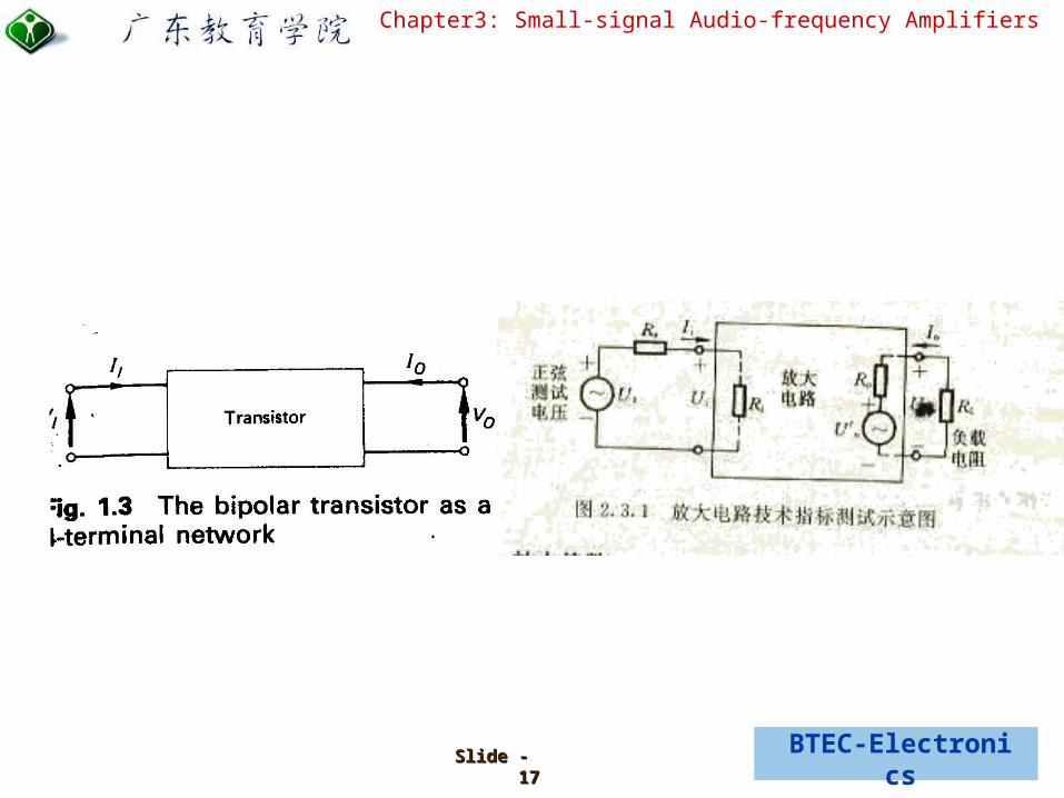
◆ Transistors and f.e.t.s may be used as amplifiers because their output currents can be controlled by an a.c. signal applied to their input terminals. ◆ A f.e.t. has such a high input impedance that its input current is negligible ; it can therefore give only a voltage gain. ◆ By suitable choice of collector current,and hence of input impedance,a transistor may be considered as either a current-operated device or a voltage-operated device. ◆ If the source impedance is much larger than the input impedance of the transistor,the transistor is current operated. If much smaller, it is voltage operate.
3.1 Principles of operation
BTEC-Electronics
Chapter3: Small-signal Audio-frequency Amplifiers
Slide - Slide - 1717

BTEC-Electronics
Chapter3: Small-signal Audio-frequency Amplifiers
Slide - Slide - 1818
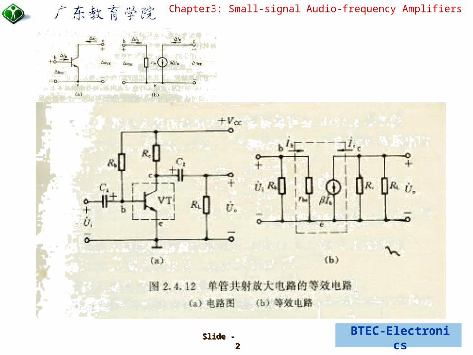
In the common-emitter connection:
input impedance:
cfe
B
Ih
I
BfeC IhI cm
BE
Ig
V
fe C BE BE
m B C B
h I V V
g I I I
imfe rgh
B
BEi I
Vr

BTEC-Electronics
Chapter3: Small-signal Audio-frequency Amplifiers
Slide - Slide - 1919
◆ The mutual characteristics of a f.e.t or a transistor always exhibit some non-linearity. If a suitable operating point is chosen and the amplitude of the input signal is limited, the operation of the circuit may be taken as linear without the introduction of undue error.
◆ The function of a small-signal amplifier is to supply a current or voltage to a load, the power output being unimportant. In a large-signal amplifier,on the other hand, the power output iS the important factor. ◆
◆
◆
3.1 Principles of operation
i
change in output currentcurrent gain A =
change in input current
v
change in output voltagevoltage gain A =
change in input voltagei L
IN
AR
R
2
p
change in output powerpower gain A =
change in input poweri L
i vIN
A RA A
R
BTEC-Electronics
Chapter3: Small-signal Audio-frequency Amplifiers
Slide - Slide - 2020
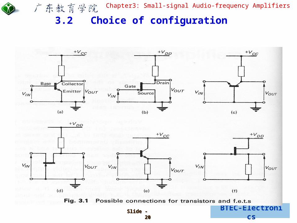
◆ The various ways in which a transistor or f.e.t.may be connected to provide a gain are shown in Fig.3.1.
3.2 Choice of configuration

BTEC-Electronics
Chapter3: Small-signal Audio-frequency Amplifiers
Slide - Slide - 2121

BTEC-Electronics
Chapter3: Small-signal Audio-frequency Amplifiers
Slide - Slide - 2222
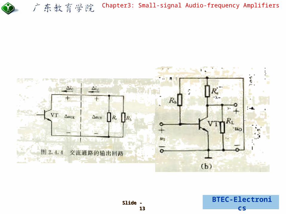
◆ The short-circuit a.c. current gain hfe of a transistor connected in the common-emitte
r configuration (Fig.3.3) is much greater than the short-circuit a.c. current gain of thesame transistor connected with common base, i.e. h
fe=h
fb/ (1- h
fb ). Resistance-capacita
nce coupling of the cascaded stages of an amplifier is possible and nowadays transformers are rarely used. Generally, common-emitter stages are biased, so that the transistor is current operated. Then the input impedance is in the region of 1000-2000Ω while the output impedance is some 10-30 kΩ.
3.2 Choice of configuration
Fig. 3.3 common-emitter amplifier

BTEC-Electronics
Chapter3: Small-signal Audio-frequency Amplifiers
Slide - Slide - 2323
◆ A transistor connected as a common-base amplifier (Fig. 3.2) has a short circuit a.c. current gain hfb less than unity (typically about 0.992), a low input
impedance of the order of 50Ω, and an output impedance of about 1 MΩ. Because the current gain is less than unity, common-base stages cannot be cascaded using resistance-capacitance coupling but transformer coupling can be used. Transformers, however, have the disadvantages of being relatively costly, bulky and heavy and having a limited frequency response, particularly the miniature types used in transistor circuits.
3.2 Choice of configuration
Fig. 3.2 common-base amplifier
BTEC-Electronics
Chapter3: Small-signal Audio-frequency Amplifiers
Slide - Slide - 2424
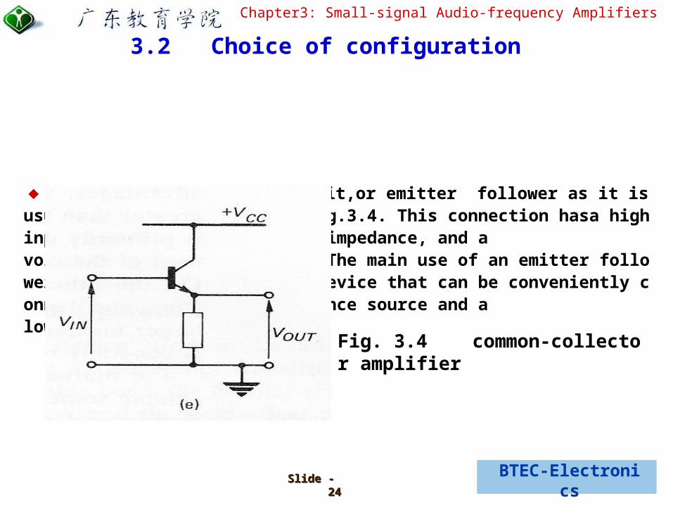
◆ The common-collector circuit,or emitter follower as it is usually called, is shown in Fig.3.4. This connection hasa high input impedance, a low output impedance, and a voltage gain less than unity. The main use of an emitter follower is as a power amplifying device that can be conveniently connected between a high-impedance source and alow-impedance load.
3.2 Choice of configuration
Fig. 3.4 common-collector amplifier

BTEC-Electronics
Chapter3: Small-signal Audio-frequency Amplifiers
Slide - Slide - 2525
◆ In the normal mode of operation (Fig.3.5), the source is common to the input and output circuits, the input signal is applied to the gate, and the output is taken frombetween drain and earth.This connection provides a large voltage gain and has a high input impedance.
3.2 Choice of configuration
Fig. 3.5 common-collector amplifier

BTEC-Electronics
Chapter3: Small-signal Audio-frequency Amplifiers
Slide - Slide - 2626
◆ Fig.3.6 shows the f.e.t. equivalent of the emitter follower, this is known as the source follower circuit. The follower circuit will be treated in greater detail in Chapter 4.
3.2 Choice of configuration
Fig. 3.5 common-collector amplifier

BTEC-Electronics
Chapter3: Small-signal Audio-frequency Amplifiers
Slide - Slide - 2727
(a) giving one of the required points.
(b) giving the second point
(c) If these two points are located on the characteristics and joined by a straight line,the load line for the particular load resistance and supply voltage is obtained.
3.3 Determination of gain using a load line
3.3.1 The relationship of output voltage and output current
CC CE C LV V I R
Let 0c DI I ;then CC CEV V
Let 0CC CEV V ;then CC C LV I R
Fig. 3.6 common-emmitter amplifier

BTEC-Electronics
Chapter3: Small-signal Audio-frequency Amplifiers
Slide - Slide - 2828
(a) giving one of the required points.
(b) giving the second point
3.3 Determination of gain using a load line
3.3.1 The relationship of output voltage and output current
Fig. 3.7 common-source amplifier
DD DS D LV V I R
Let 0c DI I ; DD DSV V
DD D LV I R

BTEC-Electronics
Chapter3: Small-signal Audio-frequency Amplifiers
Slide - Slide - 2929
3.3 Determination of gain using a load line
3.3.1 The relationship of output voltage and output current
Tab. 3.1 data of the common emmitter amplifier
example 3.1A transistor connected in the common-emitter configuration has the data
given in Table 3.1. Plot the output characteristics of the transistor and draw the load lines for collector load resistances of (a) 1000Ω and (b) 1800Ω.Use
the load lines to determine the steady (quiescent) collector current and voltage if the base bias current is 80μA and the collector supply Ic=0 Vce=Vcc=9V and is marked A in Fig.3.3.

BTEC-Electronics
Chapter3: Small-signal Audio-frequency Amplifiers
Slide - Slide - 3030
3.3 Determination of gain using a load line
3.3.2 Choice of Operating Point
Fig. 3.8 Choice of Operating Point
◆In practice, some non-linearity always exists, and to minimize signal distortion care must be taken to restrict operation to the most nearly linear part of the characteristic.
◆ For this a suitable operating point must be selected and the signal amplitude must be restricted.
BTEC-Electronics
Chapter3: Small-signal Audio-frequency Amplifiers
Slide - Slide - 3131
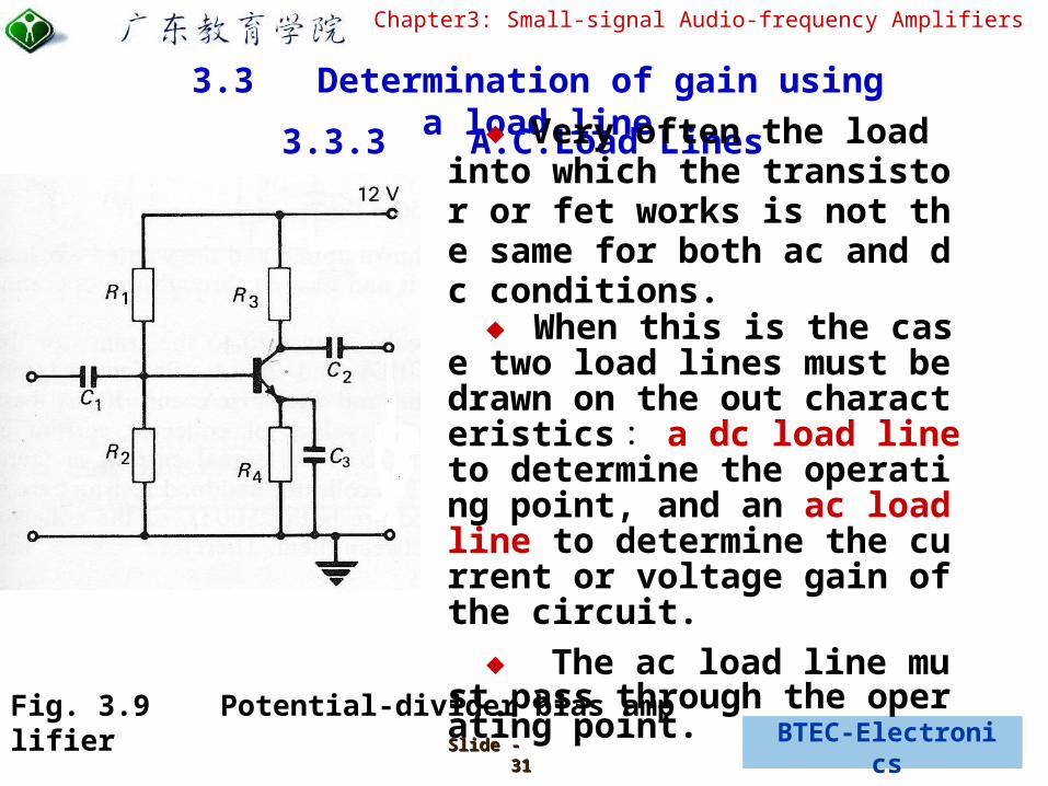
3.3 Determination of gain using a load line
3.3.3 A.C.Load Lines
Fig. 3.9 Potential-divider bias amplifier
◆ Very often the load into which the transistor or fet works is not the same for both ac and dc conditions.
◆ When this is the case two load lines must be drawn on the out characteristics : a dc load line to determine the operating point, and an ac load line to determine the current or voltage gain of the circuit.
◆ The ac load line must pass through the operating point.

BTEC-Electronics
Chapter3: Small-signal Audio-frequency Amplifiers
Slide - Slide - 3232
3.3 Determination of gain using a load line
3.3.3 A.C.Load Lines
Fig. 3.10 A.C.Load Lines

BTEC-Electronics
Chapter3: Small-signal Audio-frequency Amplifiers
Slide - Slide - 3333
3.3 Determination of gain using a load line
3.3.4 Current Gain of a Transistor Amplifier
Fig. 3.9 Potential-divider bias amplifier
◆ When an input signal is applied to a transistor amplifier, the signal current iS superimposed upon the bias current.
◆ suppose that the base bias current is IB2 and that an input signal current swings the base current between the values IB1 and IB3.
◆ The resulting values of collector current are found by projecting onto the collector-current axis from the in tersection of the a.c.load line and the curves f
or IB1 and IB3.
Fig. 3.11 Current Gain of a Transistor Amplifier

BTEC-Electronics
Chapter3: Small-signal Audio-frequency Amplifiers
Slide - Slide - 3434
3.3 Determination of gain using a load line
3.3.4 Current Gain of a Transistor Amplifier
Fig. 3.9 Potential-divider bias amplifier
Fig. 3.11 Current Gain of a Transistor Amplifier peak-to-peak collector current
peak-to-peak base currentiA
( ) ( )
3 1
C MAX C MIN
B B
I I
I I

BTEC-Electronics
Chapter3: Small-signal Audio-frequency Amplifiers
Slide - Slide - 3535
example 3.2The transistor used in the circuit has the
data given in Table. Plot the output characteristics of the transistor. Draw the dc load line and select a suitable operating point. Draw the ac load line and use it to find the alternating current that flows in the 2500Ω load when an input signal producing a base current swing of±15μA about the bias current is applied to the circuit. Assume all the capacitors have zero reactance at signal frequencies.
3.3.4 Current Gain of a Transistor Amplifier
Fig. 3.12 example 3.2
BTEC-Electronics
Chapter3: Small-signal Audio-frequency Amplifiers
Slide - Slide - 3636
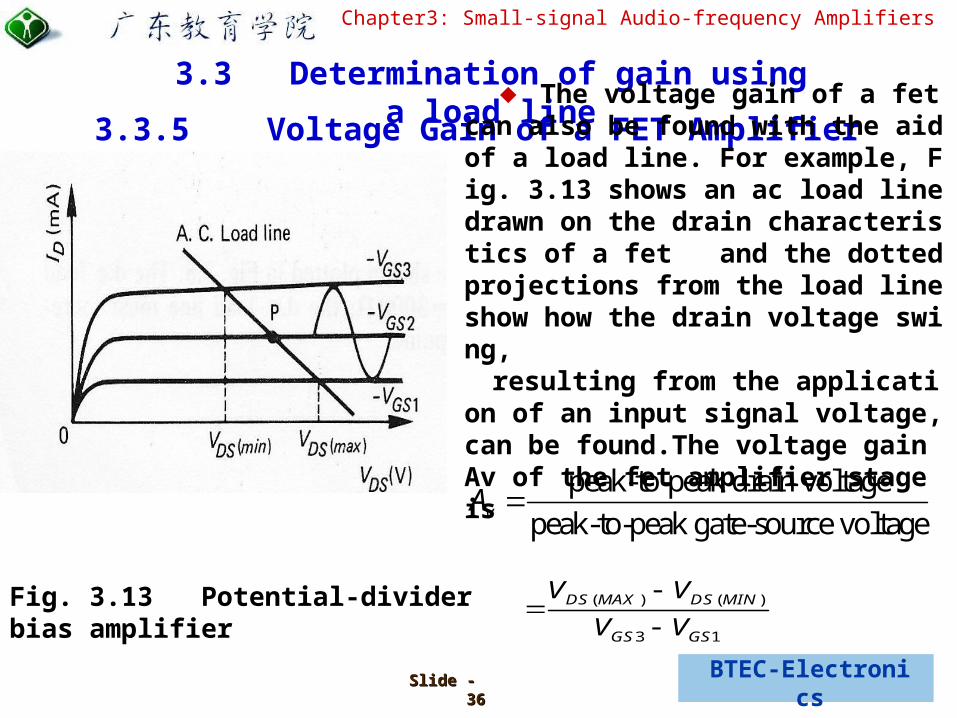
3.3 Determination of gain using a load line
3.3.5 Voltage Gain of a FET Amplifier
Fig. 3.13 Potential-divider bias amplifier
◆ The voltage gain of a fet can also be found with the aid of a load line. For example, Fig. 3.13 shows an ac load line drawn on the drain characteristics of a fet and the dotted projections from the load line show how the drain voltage swing,
resulting from the application of an input signal voltage, can be found.The voltage gain Av of the fet amplifier stage is
peak-to-peak drain voltage
peak-to-peak gate-source voltagevA
( ) ( )
3 1
DS MAX DS MIN
GS GS
V V
V V

BTEC-Electronics
Chapter3: Small-signal Audio-frequency Amplifiers
Slide - Slide - 3737
example 3.3Draw the d.c.load line and select a suitabl
eoperatin point. Draw the a.c.load line and
use it to find the voltage gain when a sinusoidal input signal of 0.3 V peak is applied.
Fig. 3.14 example 3.3
3.3.5 Voltage Gain of a FET Amplifier
BTEC-Electronics
Chapter3: Small-signal Audio-frequency Amplifiers
Slide - Slide - 3838
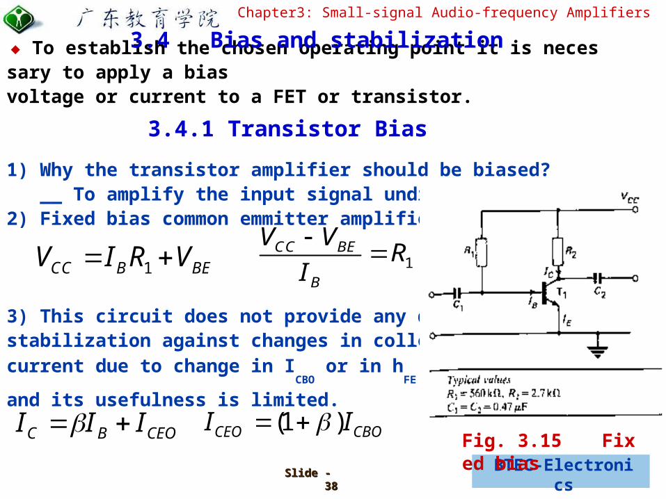
◆ To establish the chosen operating point it is necessary to apply a bias voltage or current to a FET or transistor.
1) Why the transistor amplifier should be biased? __ To amplify the input signal undistorted. 2) Fixed bias common emmitter amplifier.
3) This circuit does not provide any d.c. stabilization against changes in collector current due to change in I
CBO or in h
FE
and its usefulness is limited.
3.4 Bias and stabilization
3.4.1 Transistor Bias
1CC B BEV I R V 1CC BE
B
V VR
I
CBOCEO II )1( CEOBC III Fig. 3.15 Fixed bias

BTEC-Electronics
Chapter3: Small-signal Audio-frequency Amplifiers
Slide - Slide - 3939
EXAMPLE 3.4
The circuit shown in Fig 3.16 is designed for operation withtransistors having a nominal h
FE of 100. Calculate the collector
current. If the range of possible hFE
is from 50 to 160, calculate the collector
current flowing if a transistor having the maximum h
FE is used. Assume I
CBO=10nA and
VBE
=0.62V.
In the above example the effect of the increased collector current wouldbe to move the operating point along the d.c.load line,and this would lead to signal distortion unless the input signal level were reduced.
3.4.1 Transistor Bias
Fig. 3.16 example 3.4
Related Documents