UCC2626, UCC3626 SLUS318B – APRIL 1999 – REVISED JANUARY 2002 BRUSHLESS DC MOTOR CONTROLLER 1 www.ti.com FEATURES D Two-Quadrant and Four-Quadrant Operation D Integrated Absolute Value Current Amplifier D Pulse-by-Pulse and Average Current Sensing D Accurate, Variable Duty-Cycle Tachometer Output D Trimmed Precision Reference D Precision Oscillator D Direction Output DESCRIPTION The UCC3626 motor controller device combines many of the functions required to design a high-performance, two- or four-quadrant, three- phase, brushless dc motor controller into one package. Rotor position inputs are decoded to provide six outputs that control an external power stage. A precision triangle oscillator and latched comparator provide PWM motor control in either voltage- or current-mode configurations. The oscillator is easily synchronized to an external master clock source via the SYNCH input. Additionally, a QUAD select input configures the chip to modulate either the low-side switches only, or both upper and lower switches, allowing the user to minimize switching losses in less demanding two-quadrant applications. The device includes a differential current-sense amplifier and absolute-value circuit which provide an accurate reconstruction of motor current, useful for pulse-by-pulse overcurrent protection, as well as closing a current control loop. A precision tachometer is also provided for implementing closed-loop speed control. The TACH_OUT signal is a variable duty-cycle, frequency output, which can be used directly for digital control or filtered to provide an analog feedback signal. Other features include COAST, BRAKE, and DIR_IN commands, along with a direction output, DIR_OUT. PRODUCTION DATA information is current as of publication date. Products conform to specifications per the terms of Texas Instruments standard warranty. Production processing does not necessarily include testing of all parameters. Copyright 2002, Texas Instruments Incorporated

Welcome message from author
This document is posted to help you gain knowledge. Please leave a comment to let me know what you think about it! Share it to your friends and learn new things together.
Transcript

SLUS318B – APRIL 1999 – REVISED JANUARY 2002
1www.ti.com
FEATURES Two-Quadrant and Four-Quadrant Operation
Integrated Absolute Value Current Amplifier
Pulse-by-Pulse and Average Current Sensing
Accurate, Variable Duty-Cycle TachometerOutput
Trimmed Precision Reference
Precision Oscillator
Direction Output
DESCRIPTION
The UCC3626 motor controller device combinesmany of the functions required to design ahigh-performance, two- or four-quadrant, three-phase, brushless dc motor controller into onepackage. Rotor position inputs are decoded toprovide six outputs that control an external powerstage. A precision triangle oscillator and latchedcomparator provide PWM motor control in either
voltage- or current-mode configurations. Theoscillator is easily synchronized to an externalmaster clock source via the SYNCH input.Additionally, a QUAD select input configures thechip to modulate either the low-side switches only,or both upper and lower switches, allowing theuser to minimize switching losses in lessdemanding two-quadrant applications.
The device includes a differential current-senseamplifier and absolute-value circuit which providean accurate reconstruction of motor current,useful for pulse-by-pulse overcurrent protection,as well as closing a current control loop. Aprecision tachometer is also provided forimplementing closed-loop speed control. TheTACH_OUT signal is a variable duty-cycle,frequency output, which can be used directly fordigital control or filtered to provide an analogfeedback signal. Other features include COAST,BRAKE, and DIR_IN commands, along with adirection output, DIR_OUT.
! " #$ %!&% "! "! '! ! !( !%% )*& % "!+ %! !!$* $ %!!+ $$ "!!&
Copyright 2002, Texas Instruments Incorporated
SLUS318B – APRIL 1999 – REVISED JANUARY 2002
2 www.ti.com
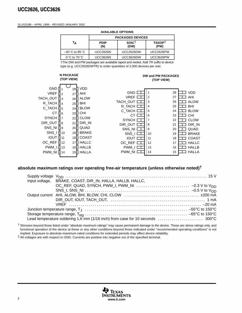
AVAILABLE OPTIONS
PACKAGED DEVICES
TA PDIP(N)
SOIC
(DW)TSSOP
(PW)
–40C to 85C UCC2626N UCC2626DW UCC2626PW
0C to 70C UCC3626N UCC3626DW UCC3626PW
The DW and PW packages are available taped and reeled. Add TR suffix to devicetype (e.g. UCC2626DWTR) to order quantities of 2,000 devices per reel.
1
2
3
4
5
6
7
8
9
10
11
12
13
14
28
27
26
25
24
23
22
21
20
19
18
17
16
15
GNDVREF
TACH_OUTR_TACHC_TACH
CTSYNCH
DIR_OUTSNS_NI
SNS_IIOUT
OC_REFPWM_I
PWM_NI
VDDAHIALOWBHIBLOWCHICLOWDIR_INQUADBRAKECOASTHALLCHALLBHALLA
N PACKAGE(TOP VIEW)
1
2
3
4
5
6
78
9
10
11
12
13
14
28
27
26
25
24
23
2221
20
19
18
17
16
15
GNDVREF
TACH_OUTR_TACHC_TACH
CTSYNCH
DIR_OUTSNS_NI
SNS_IIOUT
OC_REFPWM_I
PWM_NI
VDDAHIALOWBHIBLOWCHICLOWDIR_INQUADBRAKECOASTHALLCHALLBHALLA
DW and PW PACKAGES(TOP VIEW)
absolute maximum ratings over operating free-air temperature (unless otherwise noted)†
Supply voltage VDD 15 V. . . . . . . . . . . . . . . . . . . . . . . . . . . . . . . . . . . . . . . . . . . . . . . . . . . . . . . . . . . . . . . . . . . . . . . . Input voltage, BRAKE, COAST, DIR_IN, HALLA, HALLB, HALLC,
OC_REF, QUAD, SYNCH, PWM_I, PWM_NI –0.3 V to VDD. . . . . . . . . . . . . . . . . . . . . . . . . . . SNS_I, SNS_NI –0.5 V to VDD. . . . . . . . . . . . . . . . . . . . . . . . . . . . . . . . . . . . . . . . . . . . . . . . . . . . .
Output current AHI, ALOW, BHI, BLOW, CHI, CLOW ±200 mA. . . . . . . . . . . . . . . . . . . . . . . . . . . . . . . . . . . . . . DIR_OUT, IOUT, TACH_OUT, 1 mA. . . . . . . . . . . . . . . . . . . . . . . . . . . . . . . . . . . . . . . . . . . . . . . . VREF –20 mA. . . . . . . . . . . . . . . . . . . . . . . . . . . . . . . . . . . . . . . . . . . . . . . . . . . . . . . . . . . . . . . . . . .
Junction temperature range, TJ –55°C to 150°C. . . . . . . . . . . . . . . . . . . . . . . . . . . . . . . . . . . . . . . . . . . . . . . . . . . . Storage temperature range, Tstg –65°C to 150°C. . . . . . . . . . . . . . . . . . . . . . . . . . . . . . . . . . . . . . . . . . . . . . . . . . . . Lead temperature soldering 1,6 mm (1/16 inch) from case for 10 seconds 300°C. . . . . . . . . . . . . . . . . . . . . . .
† Stresses beyond those listed under “absolute maximum ratings” may cause permanent damage to the device. These are stress ratings only, andfunctional operation of the device at these or any other conditions beyond those indicated under “recommended operating conditions” is notimplied. Exposure to absolute-maximum-rated conditions for extended periods may affect device reliability.
‡ All voltages are with respect to GND. Currents are positive into negative out of the specified terminal.

SLUS318B – APRIL 1999 – REVISED JANUARY 2002
3www.ti.com
block diagram
UDG–97173
17HALLC
8DIR_OUT
14PWM_NI
13PWM_I
16HALLB
SYNCH
11
OC_REF
9
SNS_I
3
4
1
5
22 CLOW
C_TACH
R_TACH
TACH_OUT
GND
2 VREF
27 AHI
25 BHI
23 CHI
26 ALOW
10
SNS_NI
IOUT
7
6
12
CT
18COAST
21DIR_IN
15HALLA
19BRAKE
20QUAD
SENSE AMPLIFIER
OVERCURRENTCOMPARATOR
OSCILLATOR
DIRECTIONDETECTOR EDGE
DETECTOR
28 VDD
ONESHOT
5 VOLTREFERENCE
S
R
PWM LOGIC
24 BLOW
1.75V
DIRECTIONSELECT
HALLDECODER
PWMCOMPARATOR
X5
S
R
RxC
Q
Q
Q
Q

SLUS318B – APRIL 1999 – REVISED JANUARY 2002
4 www.ti.com
electrical characteristics over recommended operating conditions, VCC = 12 V; CT = 1 nF, R_TACH = 250 kΩ, C_TACH = 100 pF, TA = TJ, TA = –40°C to 85°C for the UCC2626, and 0°C to 70°Cfor the UCC3626 (unless otherwise noted)
overallPARAMETER TEST CONDITIONS MIN TYP MAX UNIT
Supply current Outputs not switching 1 3 5 mA
undervoltage lockoutPARAMETER TEST CONDITIONS MIN TYP MAX UNIT
Start threshold 9.0 10.5 11.0 V
UVLO hysteresis 0.35 0.40 0.50 V
5-V referencePARAMETER TEST CONDITIONS MIN TYP MAX UNIT
Output voltage IVREF = –2 mA 4.9 5 5.1 V
Line regulation voltage 11 V < VCC < 14.5 V 10 mV
Load regulation voltage –1 mA > IVREF > –5 mA 10 mV
Short circuit current 40 120 240 mA
coast input comparatorPARAMETER TEST CONDITIONS MIN TYP MAX UNIT
Threshold voltage 1.60 1.75 2.00 V
Hysteresis 0.04 0.10 0.16 V
current sense amplifierPARAMETER TEST CONDITIONS MIN TYP MAX UNIT
Input offset voltage VCM = 0 V 8 mV
Input bias current VCM = 0 V 5 10 15 µA
Gain VCM = 0 V 4.85 5.00 5.15 V/V
PSRR 11 V < VCC < 14.5 V 60 dB
High-level output voltage IIOUT= –100 µA 6.3 V
Low-level output voltage IIOUT = 100 µA 70 mV
Output source currentUCC3626 VIOUT = 2 V 500 µA
Output source currentUCC2626 VIOUT = 2 V 300 µA
pwm comparatorPARAMETER TEST CONDITIONS MIN TYP MAX UNIT
Input common mode range 2.0 8.0 V
Propagation delay time 75 150 ns
overcurrent comparatorPARAMETER TEST CONDITIONS MIN TYP MAX UNIT
Input common mode range 0.0 5.0 V
Propagation delay time 50 175 250 ns
logic inputsPARAMETER TEST CONDITIONS MIN TYP MAX UNIT
High-level logic input voltage QUAD, BRAKE, DIR, SYNCH 3.6 V
Low-level logic input voltage QUAD, BRAKE, DIR, SYNCH 1.4 V

SLUS318B – APRIL 1999 – REVISED JANUARY 2002
5www.ti.com
electrical characteristics over recommended operating conditions, VCC = 12 V; CT = 1 nF, R_TACH = 250 kΩ, C_TACH = 100 pF, TA = TJ, TA = –40°C to 85°C for the UCC2626, and 0°C to 70°Cfor the UCC3626 (unless otherwise noted)
hall buffer inputsPARAMETER TEST CONDITIONS MIN TYP MAX UNIT
High-level input voltage HALLA, HALLB, HALLC 1.7 1.9 2.1 V
Hysteresis HALLA, HALLB, HALLC 0.6 1.0 V
Input current 0V < VIN < 5 V –25 µA
oscillatorPARAMETER TEST CONDITIONS MIN TYP MAX UNIT
Frequency RTACH = 250 kΩ, CT = 1nF 9.0 10.0 11.0 kHz
Frequency change with voltage 12 V < VCC < 14.5 V 3%
CT peak voltage 7.25 7.5 7.75 V
CT peak-to-valley voltage 4.75 5.0 5.25 V
SYNCH pin minimum pulse width 500 ns
tachometerPARAMETER TEST CONDITIONS MIN TYP MAX UNIT
High-level output voltage/VREF IOUT = –10 µA 99% 100%
Low-level output voltage IOUT = 10 µA 0 20 mV
High-level on-resistance IOUT = –100 µA 1 1.5 kΩ
Low-level on-resistance IOUT = 100 µA 1 1.5 kΩ
High-level ramp threshold voltage 2.5 V
Ramp voltage 2.375 2.500 2.625 V
CTACH charge current RTACH = 49.9 kΩ 48 51 53 µA
On time accuracyUCC3626 See Note 1 –3% 3%
On-time accuracyUCC2626 See Note 1 –4% 3%
direction outputPARAMETER TEST CONDITIONS MIN TYP MAX UNIT
High-level output voltage IOUT = –100 µA 4.5 5.2 V
Low-level output voltage IOUT = 100 µA 0 0.5 V
outputPARAMETER TEST CONDITIONS MIN TYP MAX UNIT
Maximum duty cycle 100%
Lo le el o tp t oltageIOUT = 2 mA 0.0 0.1 0.5 V
Low-level output voltageIOUT = 100 µA 0.0 0.1 V
High level output voltageIOUT = –2 mA 4.0 4.8 5.2 V
High-level output voltageIOUT = –100 µA 4.7 5.2 V
Rise and fall time CI = 10 pF 100 ns
NOTE 1: tON is calculated using the formula tON CTACH VHI VLO
ICHARGE

SLUS318B – APRIL 1999 – REVISED JANUARY 2002
6 www.ti.com
pin descriptions
AHI, BHI, CHI: Digital outputs used to control the high-side switches in a three-phase inverter. For specificdecoding information reference Table I.
ALOW, BLOW, CLOW: Digital outputs used to control the low-side switches in a three-phase inverter. Forspecific decoding information reference Table I.
BRAKE: BRAKE is a digital input which causes the device to enter brake mode. In brake mode all three high-side outputs (AHI, BHI & CHI) are turned off, while all three lowside outputs (ALOW, BLOW, CLOW) are turnedon. During brake mode the tachometer output remains operational. The only conditions that can inhibit thelow-side commands during brake are UVLO, exceeding peak current, the output of the PWM comparator, orthe COAST command.
COAST: The COAST input consists of a hysteretic comparator which disables the outputs. The input is usefulin implementing an overvoltage bus clamp in four-quadrant applications. The outputs are disabled when theinput is above 1.75 V.
CT: This pin is used in conjunction with the R_TACH pin to set the frequency of the oscillator. A timing capacitoris normally connected between this point and ground and is alternately charged and discharged between 2.5 Vand 7.5 V.
C_TACH: A timing capacitor is connected between this pin and ground to set the width of the TACH_OUT pulse.The capacitor is charged with a current set by the resistor on pin R_TACH .
DIR_IN: DIR_IN is a digital input which determines the order in which the HALLA, HALLB, and HALLC inputsare decoded. For specific decode information reference Table I.
DIR_OUT: DIR_OUT represents the actual direction of the rotor as decoded from the HALLA, HALLB, andHALLC inputs. For any valid combination of HALLA, HALLB, and HALLC inputs there are two valid transitions;one of which translates to a clockwise rotation and another which translates to a counterclockwise rotation. Thepolarity of DIR_OUT is the same as DIR_IN while motoring, (i.e. sequencing from top to bottom in Table 1.)
GND: GND is the reference ground for all functions of the part. Bypass and timing capacitors should beterminated as close as possible to this point.
HALLA, HALLB, HALLC: These three inputs are designed to accept rotor position information positioned 120°apart. For specific decode information reference Table I. These inputs should be externally pulled up to VREFor another appropriate external supply.
IOUT: IOUT represents the output of the current sense and absolute value amplifiers. The output signalappearing is a representation of the following expression:
IOUT ABSISNS_I ISNS_NI 5
This output can be used to close a current control loop as well as provide additional filtering of the current sensesignal.
OC_REF: OC_REF is an analog input which sets the trip voltage of the overcurrent comparator. The sense inputof the comparator is internally connected to the output of the current sense amplifier and absolute value circuit.
PWM_NI: PWM_NI is the noninverting input to the PWM comparator.
PWM_I: PWM_I is the inverting input to the PWM comparator.
QUAD: The QUAD input selects between two-quadrant operation (QUAD = 0) and four-quadrant operation(QUAD = 1) . When in two-quadrant mode, only the low-side devices are effected by the output of the PWMcomparator. In four-quadrant mode both high- and low-side devices are controlled by the PWM comparator.

SLUS318B – APRIL 1999 – REVISED JANUARY 2002
7www.ti.com
pin descriptions
SYNCH: The SYNCH input is used to synchronize the PWM oscillator with an external digital clock. When usingthe SYNCH feature, a resistor equal to R_TACH must be placed in parallel with CT. When not using the SYNCHfeature, SYNCH must be grounded.
SNS_NI, SNS_I: These inputs are the noninverting and inverting inputs to the current sense amplifier,respectively. The integrated amplifier is configured for a gain of five. An absolute value function is alsoincorporated into the output in order to provide a representation of actual motor current when operating infour-quadrant mode.
TACH_OUT: TACH_OUT is the output of a monostable triggered by a change in the commutation state, thusproviding a variable duty cycle, frequency output. The on time of the monostable is set by the timing capacitorconnected to C_TACH. The monostable is capable of being retriggered if a commutation occurs during itson-time.
R_TACH: A resistor connected between R_TACH and ground programs the current for both the oscillator andtachometer.
VDD: VDD is the input supply connection for this device. Undervoltage lockout keeps the outputs off for inputsbelow 10.5 V. The input should be bypassed with a 0.1-µF ceramic capacitor, minimum.
VREF: VREF is a 5-V, 2% trimmed reference output with 5 mA of maximum available output current. This pinshould be bypassed to ground with a ceramic capacitor with a value of at least 0.1 µF.
APPLICATION INFORMATION
Table 1 provides the decode logic for the six outputs, AHI, BHI, CHI, ALOW, BLOW, and CLOW as a functionof the BRAKE, COAST, DIR_IN, HALLA, HALLB, and HALLC inputs.
Table 1. Commutation Truth Table
BRAKE COAST DIR_INHALL
INPUTSHIGH-SIDEOUTPUTS
LOW-SIDEOUTPUTSBRAKE COAST DIR_IN
A B C A B C A B C
0 0 1 1 0 1 1 0 0 0 1 0
0 0 1 1 0 0 1 0 0 0 0 1
0 0 1 1 1 0 0 1 0 0 0 1
0 0 1 0 1 0 0 1 0 1 0 0
0 0 1 0 1 1 0 0 1 1 0 0
0 0 1 0 0 1 0 0 1 0 1 0
0 0 0 1 0 1 0 1 0 1 0 0
0 0 0 0 0 1 0 1 0 0 0 1
0 0 0 0 1 1 1 0 0 0 0 1
0 0 0 0 1 0 1 0 0 0 1 0
0 0 0 1 1 0 0 0 1 0 1 0
0 0 0 1 0 0 0 0 1 1 0 0
X 1 X X X X 0 0 0 0 0 0
1 0 X X X X 0 0 0 1 1 1
0 0 X 1 1 1 0 0 0 0 0 0
0 0 X 0 0 0 0 0 0 0 0 0
SLUS318B – APRIL 1999 – REVISED JANUARY 2002
8 www.ti.com
APPLICATION INFORMATION
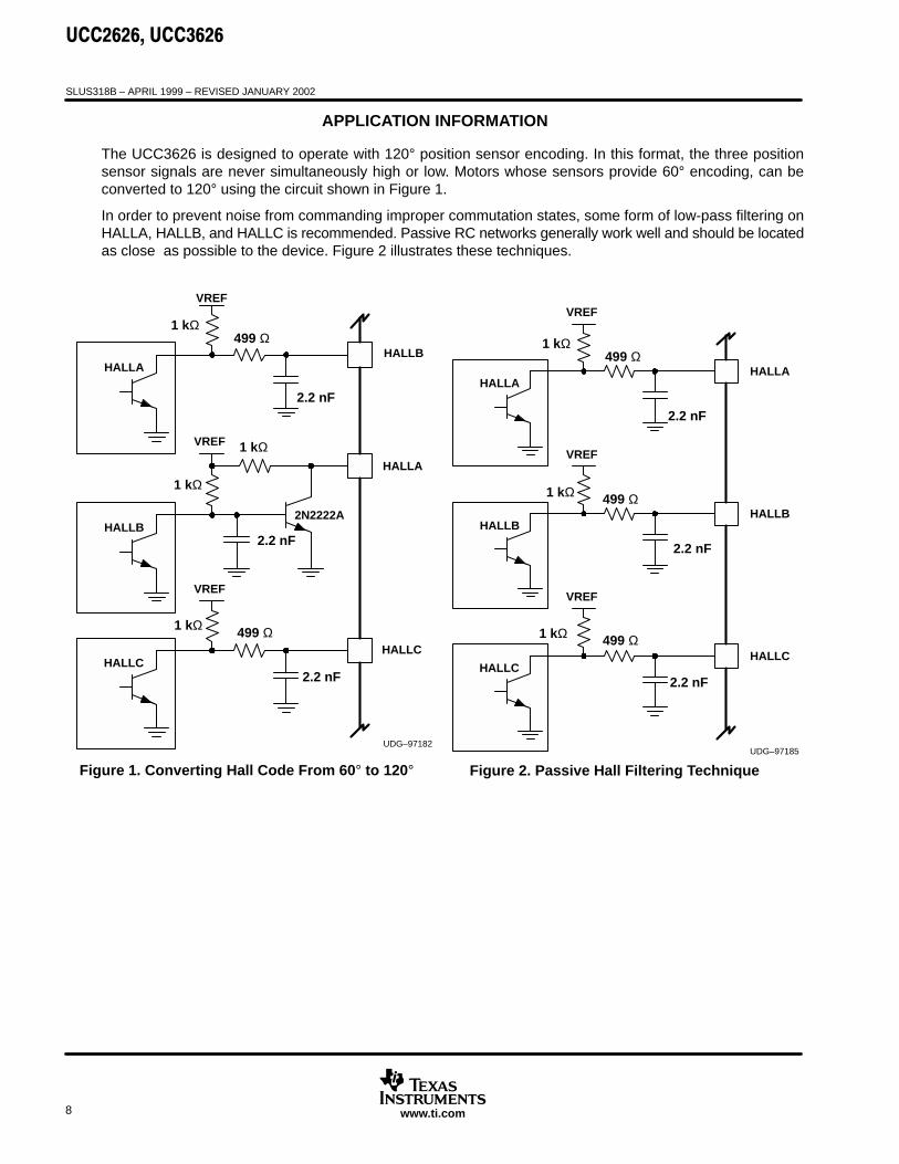
The UCC3626 is designed to operate with 120° position sensor encoding. In this format, the three positionsensor signals are never simultaneously high or low. Motors whose sensors provide 60° encoding, can beconverted to 120° using the circuit shown in Figure 1.
In order to prevent noise from commanding improper commutation states, some form of low-pass filtering onHALLA, HALLB, and HALLC is recommended. Passive RC networks generally work well and should be locatedas close as possible to the device. Figure 2 illustrates these techniques.
HALLA
HALLB
HALLC
VREF
2N2222A
HALLA
HALLB
VREF
HALLC
1 kΩ499 Ω
1 kΩ
1 kΩ
499 Ω1 kΩ
2.2 nF
2.2 nF
2.2 nF
UDG–97182
Figure 1. Converting Hall Code From 60° to 120°
VREF
HALLA
HALLB
HALLC
VREF
HALLA
HALLB
VREF
HALLC
VREF
1 kΩ499 Ω
499 Ω1 kΩ
499 Ω1 kΩ
2.2 nF
2.2 nF
2.2 nF
UDG–97185
Figure 2. Passive Hall Filtering Technique

SLUS318B – APRIL 1999 – REVISED JANUARY 2002
9www.ti.com
APPLICATION INFORMATION
configuring the oscillator
The UCC3626 oscillator is designed to operate at frequencies up to 250 kHz and provide a triangle waveformon CT with a peak-to-peak amplitude of 5 V for improved noise immunity. The current used to program CT isderived from the R_TACH resistor according to the following equation:
IOSC 25R_TACH
Amps
The oscillator frequency is set by R_TACH and CT according to the following relationship:
fOSC 2.5R_TACH CT
Hz
Timing resistor values should be between 25 kΩ and 500 kΩ, while capacitor values should be between 100 pFand 1 µF. Figure 3 provides a graph of oscillator frequency for various combinations of timing components. Aswith any high-frequency oscillator, timing components should be located as close as possible to the device pinswhen laying out the printed-circuit board. It is also important to reference the timing capacitor directly to theground pin on the UCC3626 rather than daisy chaining it to another trace or the ground plane. This techniqueprevents switching current spikes in the local ground from causing jitter in the oscillator.
synchronizing the oscillator
A common system specification is to have all oscillators synchronized to a master clock. The UCC3626 providesa SYNCH input for this purpose. The SYNCH input is designed to interface with a digital clock pulse generatedby the master oscillator. A positive-going edge on this input causes the UCC3626 oscillator to begin discharging.In order for the slave oscillator to function properly, it must be programmed for a frequency slightly lower thanthat of the master. Also, a resistor equal to R_TACH must be placed in parallel with CT. Figure 4 illustrates thewaveforms for a slave oscillator programmed to 20 kHz with a master frequency of 30 kHz. The SYNCH pinmust be grounded when not used.
Figure 3
1.E+03
1.E+04
1.E+05
1.E+06
1.E–10 1.E–09 1.E–08 1.E–07
R_TACH = 25 kΩ
R_TACH = 100 kΩ
R_TACH = 500 kΩ
R_TACH = 250 kΩ
CT – Oscillator Timing Capacitance – F
f OS
C –
PW
M F
req
uen
cy –
Hz
OSCILLATOR FREQUENCYvs
TIMING CAPACITANCE
(1)
(2)

SLUS318B – APRIL 1999 – REVISED JANUARY 2002
10 www.ti.com
APPLICATION INFORMATION
programming the tachometer
The UCC3626 tachometer consists of a precision 5-V monostable, triggered by either a rising or falling edgeon any of the three Hall inputs, HALLA, HALLB, and HALLC. The resulting TACH_OUT waveform is a variableduty-cycle square wave whose frequency is proportional to motor speed, as given by:
TACH_OUT V P20
Hz
where P is the number of motor pole pairs and V is motor velocity in RPM.
The on time of the monostable is programmed via timing resistor R_TACH and capacitor C_TACH accordingto the following equation:
tON R_TACH C_TACH sec
Figure 5 provides a graph of on times for various combinations of R_TACH and C_TACH. On time is typicallyset to a value less than the minimum TACH_OUT period as given by:
tPERIOD (min) 20
VMAX Psec
where P is the number of motor pole pairs and V is motor velocity in RPM.
SYNCH
CT
WITHOUT SYNCH
WITH SYNCH
Figure 4. Oscillator Waveforms Figure 5
1.E–06
1.E–05
1.E–04
1.E–03
1.E–02
1.E–01
1.E+00
1.E–10 1.E–09 1.E–08 1.E–07 1.E–06
R_TACH = 250 kΩ
R_TACH = 25 kΩ
R_TACH = 100 kΩ
R_TACH = 500 kΩ
t ON
– T
ach
om
eter
On
–Tim
e –
s
C_TACH – Tachometer Timing Capacitance – F
TACHOMETER ON-TIMEvs
TIMING CAPACITANCE
(3)
(4)
(5)

SLUS318B – APRIL 1999 – REVISED JANUARY 2002
11www.ti.com
APPLICATION INFORMATION
The TACH_OUT signal can be used to close a digital velocity loop using a microcontroller, as shown in Figure 6,or directly low-pass filtered in an analog implementation, Figure 7.
UDG–97188
5
4
14
R_TACH
C_TACH
PWM_NI
PWM_I13
TACH_OUT3
6 CT
UCC3626
VOUT
AD558
VCE
VCS
IC1
PC0
MC68HC11
PB0–PB7 DB0–DB7
VOUTSENSE
VOUTSELECT
Figure 6. Digital Velocity Loop Implementation Using MC68HC11
two quadrant vs four quadrant control
Figure 8 illustrates the four possible quadrants of operation for a motor. Two-quadrant control refers to a systemin which operation is limited to quadrants I and III (where torque and velocity are in the same direction). Witha two-quadrant brushless dc amplifier, there are no provisions other than friction to decelerate the load, limitingthe approach to less demanding applications. Four-quadrant controllers, on the other hand, provide controlledoperation in all quadrants, including II and IV, where torque and rotation are of opposite direction.
2
5
4
14
VREF
R_TACH
C_TACH
PWM_NI
PWM_I13
TACH_OUT3
6 CT
+
–
UCC3626
Figure 7. Simple Analog Velocity Loop
UDG–97189
I
IVIII
II
VELOCITYCW
CCW
TORQUECWCCW
UDG–01118
Figure 8. Four Quadrants of Operation
SLUS318B – APRIL 1999 – REVISED JANUARY 2002
12 www.ti.com
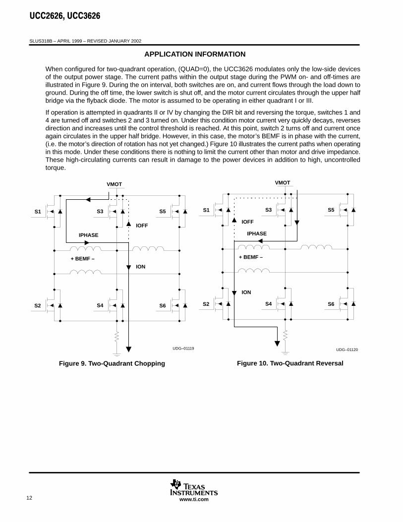
APPLICATION INFORMATION
When configured for two-quadrant operation, (QUAD=0), the UCC3626 modulates only the low-side devicesof the output power stage. The current paths within the output stage during the PWM on- and off-times areillustrated in Figure 9. During the on interval, both switches are on, and current flows through the load down toground. During the off time, the lower switch is shut off, and the motor current circulates through the upper halfbridge via the flyback diode. The motor is assumed to be operating in either quadrant I or III.
If operation is attempted in quadrants II or IV by changing the DIR bit and reversing the torque, switches 1 and4 are turned off and switches 2 and 3 turned on. Under this condition motor current very quickly decays, reversesdirection and increases until the control threshold is reached. At this point, switch 2 turns off and current onceagain circulates in the upper half bridge. However, in this case, the motor’s BEMF is in phase with the current,(i.e. the motor’s direction of rotation has not yet changed.) Figure 10 illustrates the current paths when operatingin this mode. Under these conditions there is nothing to limit the current other than motor and drive impedance.These high-circulating currents can result in damage to the power devices in addition to high, uncontrolledtorque.
Figure 9. Two-Quadrant Chopping
IPHASE
+ BEMF –
VMOT
IOFF
ION
S1 S3 S5
S2 S4 S6
UDG–01119
Figure 10. Two-Quadrant Reversal
IPHASE
+ BEMF –
VMOT
IOFF
ION
S1 S3 S5
S2 S4 S6
UDG–01120

SLUS318B – APRIL 1999 – REVISED JANUARY 2002
13www.ti.com
APPLICATION INFORMATION
By pulse width modulating both the upper and lower power devices (QUAD=1), motor current always decaysduring the PWM off time, eliminating any uncontrolled circulating currents. In addition, current always flowsthrough the current sense resistor, providing a suitable feedback signal. Figure 11 illustrates the current pathsduring a four-quadrant torque reversal. Motor drive waveforms for both two- and four-quadrant operation areillustrated in Figure 12.
UDG–01121
IPHASE
+ BEMF –
VMOT
IOFF
ION
S1 S3 S5
S2 S4 S6
Figure 11. Four-Quadrant Reversal

SLUS318B – APRIL 1999 – REVISED JANUARY 2002
14 www.ti.com
APPLICATION INFORMATION
UDG–97190
0 60 120 180 240 300 360 420 480 540 600 660 720
ROTOR POSITION IN ELECTRICAL DEGREES
Code 101 100 110 010 011 001 101 100 110 010 011 001
H1
H2
H3
AHI
BHI
CHI
ALO
BLO
CLO
+
0
–
A
+
0
–
B
+
0
–
C
MOTORPHASE
CURRENTSQUAD=0
LOW SIDEOUTPUTS
QUAD=0
HIGH SIDEOUTPUTS
QUAD=0
SENSORINPUTS
AHI
BHI
CHI
ALO
BLO
CLO
+
0
–
A
+
0
–
B
+
0
–
C
MOTORPHASE
CURRENTSQUAD=1
LOW SIDEOUTPUTS
QUAD=1
HIGH SIDEOUTPUTS
QUAD=1
100% Duty Cycle PWM 50% Duty Cycle PWM
Figure 12. Motor Drive and Current Waveforms for Two-Quadrant (QUAD=0) and Four-Quadrant (QUAD=1) Operation

SLUS318B – APRIL 1999 – REVISED JANUARY 2002
15www.ti.com
APPLICATION INFORMATION
power stage design considerations
The flexible architecture of the UCC3626 requires the user to pay close attention to the design of the poweroutput stage. Two- and four-quadrant applications not requiring the brake function are able to use the powerstage approach illustrated in Figure 13a. In many cases the body diode of the MOSFET can be used to reduceparts count and cost. If efficiency is a key requirement, Schottky diodes can be used in parallel with the switches.
UDG–97190
(b) (c)
TOMOTOR
VMOT
CURRENTSENSE
TOMOTOR
VMOT
CURRENTSENSE
TOMOT
VMOT
CURRENTSENSE
(a) UDG–01122
TWO FOUR SAFE POWERCURRENT SENSE
TWOQUADRANT
FOURQUADRANT
SAFEBRAKING
POWERREVERSAL PULSE-BY-
PULSE AVERAGE
(a) YES YES NO Four-Quad Only YES YES
(b) YES NO YES No YES NO
(c) YES YES YES Four-Quad Only YES YES
Figure 13. Power Stage Topologies
If the system requires a braking function, diodes must be added in series with the lower power devices and thelower flyback diodes must be returned to ground, as pictured in Figure 13b, and 13c. This requirement preventsbrake currents from circulating in the lower half bridge and bypassing the sense resistor. In addition, thecombination of braking and four-quadrant control necessitates an additional resistor in the diode path to sensecurrent during the PWM off time as illustrated in Figure 13c.
SLUS318B – APRIL 1999 – REVISED JANUARY 2002
16 www.ti.com
APPLICATION INFORMATION
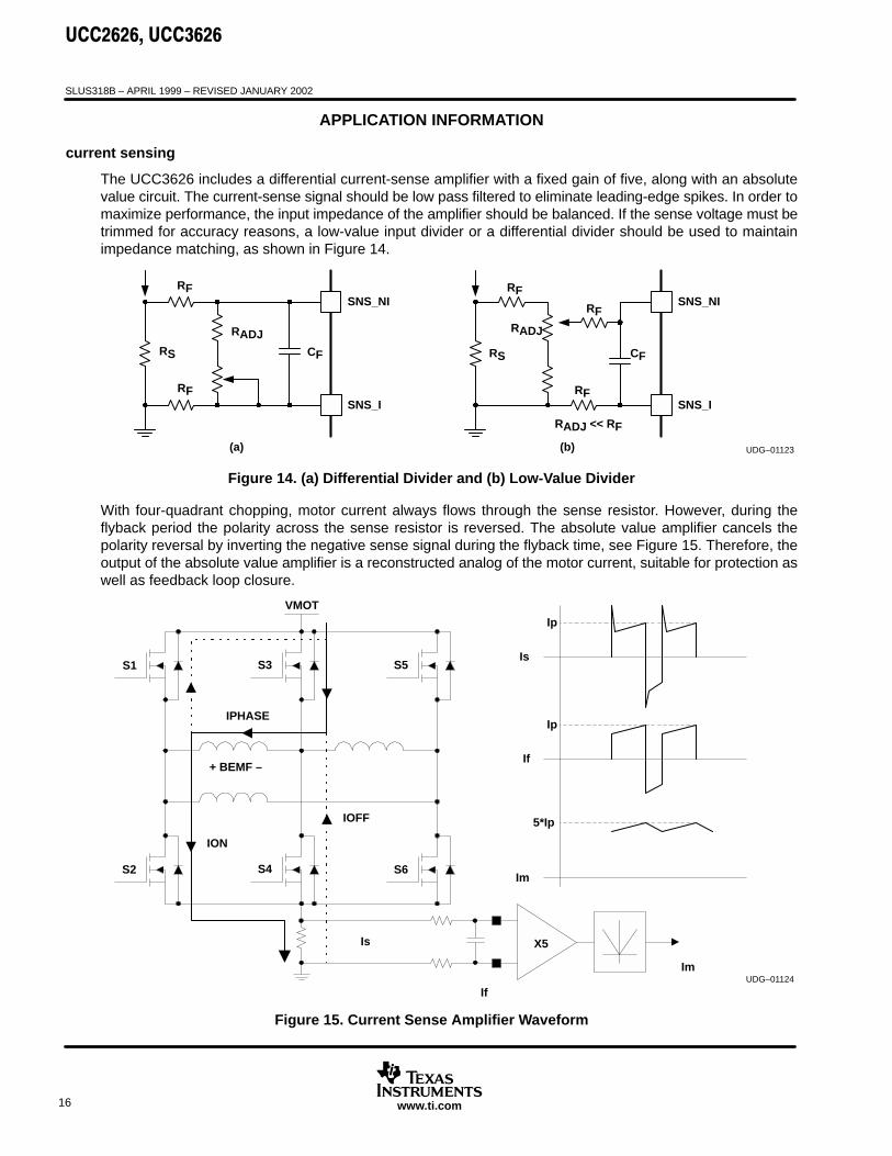
current sensing
The UCC3626 includes a differential current-sense amplifier with a fixed gain of five, along with an absolutevalue circuit. The current-sense signal should be low pass filtered to eliminate leading-edge spikes. In order tomaximize performance, the input impedance of the amplifier should be balanced. If the sense voltage must betrimmed for accuracy reasons, a low-value input divider or a differential divider should be used to maintainimpedance matching, as shown in Figure 14.
UDG–01123
RF
RADJ
RF
RS CF
RF
RADJ
RF
RS CF
SNS_NI
SNS_I
(a)
SNS_NI
SNS_I
(b)
RF
RADJ << RF
Figure 14. (a) Differential Divider and (b) Low-Value Divider
With four-quadrant chopping, motor current always flows through the sense resistor. However, during theflyback period the polarity across the sense resistor is reversed. The absolute value amplifier cancels thepolarity reversal by inverting the negative sense signal during the flyback time, see Figure 15. Therefore, theoutput of the absolute value amplifier is a reconstructed analog of the motor current, suitable for protection aswell as feedback loop closure.
UDG–01124
IPHASE
+ BEMF –
VMOT
IOFF
ION
S1 S3 S5
S2 S4 S6
X5Is
If
Im
Is
If
Im
Ip
Ip
5*Ip
Figure 15. Current Sense Amplifier Waveform

SLUS318B – APRIL 1999 – REVISED JANUARY 2002
17www.ti.com
APPLICATION INFORMATION
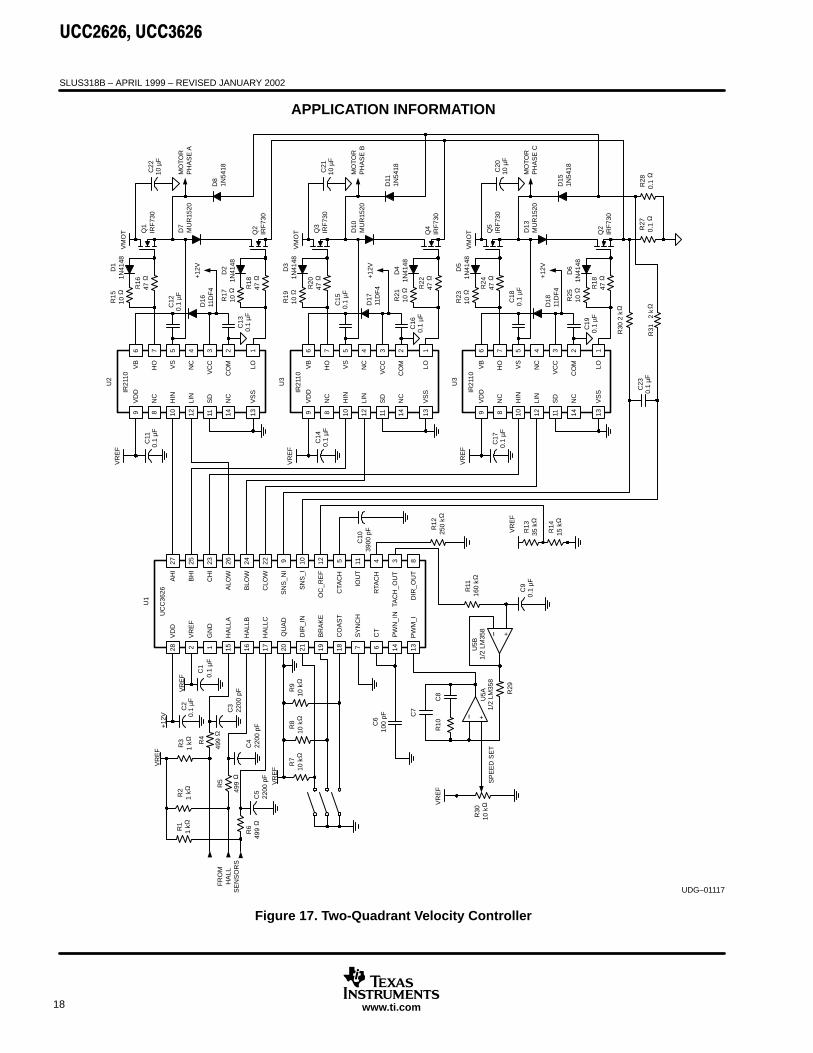
Figure 17 illustrates a simple 175-V, 2-A, two-quadrant velocity controller using the UCC3626. The power stageis designed to operate with a rectified off-line supply using IR2210s to provide the interface between the lowvoltage control signals and the power MOSFETs. The power topology illustrated in Figure 13c is implementedin order to provide braking capability.
UDG–99061
11 IOUT
+
–13 PWM_I
CURRENTERRORAMPLIFIER
+
–U6
+
–
SIGN/MAGNITUDE CONVERTER
21 DIRU7
CURRENT SIGN
3 TACH_OUT+
–U2
TACHOMETERFILTER
2N70028 DIR_OUT
+
–U3
BIPOLARTACH GAIN
+
–U1
CURRENTMAGNITUDE
U5
U8
10 kΩ 10 kΩ 10 kΩ 10 kΩ
10 kΩ
10 kΩ
4.99 kΩ 4.99 kΩ
10 kΩ
VELOCITYCOMMAND
± 5 V
Figure 16. Four-Quadrant Control Loop
The controller’s speed command is set by potentiometer R30, while the speed feedback signal is obtained bylow-pass filtering and buffering the TACH_OUT signal using R11 and C9. Small signal compensation of thevelocity control loop is provided by amplifier U5A, whose output is used to control the PWM duty cycle. Theintegrating capacitor, C8, places a pole at 0 Hz and a zero in conjunction with R10. This zero can be used tocancel the low-frequency motor pole and to cross the loop-over with a –20 dB gain response.
Four-quadrant applications require the control of motor current. Figure 16 illustrates a sign/magnitude currentcontrol loop within an outer bipolar velocity loop using the UCC3626. U1 serves as the velocity loop erroramplifier and accepts a ± 5-V command signal. Velocity feedback is provided by low-pass filtering and scalingthe TACH_OUT signal using U2. The direction output switch, DIR_OUT, and U3 set the polarity of thetachometer gain according to the direction of rotation. The output of the velocity error amplifier, U1, is thenconverted to sign/magnitude form using U5 and U6. The sign portion is used to drive the DIR input while themagnitude commands the current error amplifier, U8. Current feedback is provided by the internal current senseamplifier via the IOUT pin.
SLUS318B – APRIL 1999 – REVISED JANUARY 2002
18 www.ti.com
APPLICATION INFORMATION
UDG–01117
9 8 10 12 11 14 13
6 7 5 4 3 12
VD
D
NC
HIN
LIN
SD
NC
VS
S
VB
HO VS
NC
VC
C
LO
CO
M
U2
IR21
10
D16
11D
F4 R
1847
Ω
R17
10Ω
D2
1N41
48
D7
MU
R15
20+
12V
D1
1N41
48R
1510
Ω
R16
47Ω
D8
1N54
18
Q2
IRF
730
MO
TOR
PH
AS
E A
VM
OT
VR
EF
Q1
IRF
730
28 2 1 15 16 17 20
27 25 23 26 24 922
VD
D
VR
EF
GN
D
HA
LLA
HA
LLB
HA
LLC
QU
AD
AH
I
BH
I
CH
I
ALO
W
BLO
W
SN
S_N
I
CLO
W
U1
UC
C36
26
10 11 8512
SN
S_I
IOU
T
DIR
_OU
T
CTA
CH
OC
_RE
F
34
TAC
H_O
UT
RTA
CH
21 19 18 67 1314
DIR
_IN
BR
AK
E
CO
AS
T
SY
NC
H
CT
PW
N_I
N
PW
M_I
9 8 10 12 11 14 13
6 7 5 4 3 12
VD
D
NC
HIN
LIN
SD
NC
VS
S
VB
HO VS
NC
VC
C
LO
CO
M
U3
IR21
10
D17
11D
F4 R
2247
Ω
R21
10Ω
D4
1N41
48
D10
MU
R15
20+
12V
D3
1N41
48R
1910
Ω
R20
47Ω
D11
1N54
18
Q4
IRF
730
MO
TOR
PH
AS
E B
VM
OT
VR
EF
Q3
IRF
730
9 8 10 12 11 14 13
6 7 5 4 3 12
VD
D
NC
HIN
LIN
SD
NC
VS
S
VB
HO VS
NC
VC
C
LO
CO
M
U3
IR21
10
D18
11D
F4 R
1847
Ω
R25
10Ω
D6
1N41
48
D13
MU
R15
20+
12V
D5
1N41
48R
2310
Ω
R24
47Ω
D15
1N54
18
Q2
IRF
730
MO
TOR
PH
AS
E C
VM
OT
VR
EF
Q5
IRF
730
R30
2 k
Ω
R31
2
kΩ
R13
35 k
Ω
VR
EF
R14
15 k
Ω
R12
250
kΩ
C10
3900
pF
R11
160
kΩ
+
U5B
1/2
LM35
8
R29
+
R10
C8
C7
C6
100
pF
R9
10 k
ΩR
810
kΩ
R7
10 k
Ω
VR
EF
C5
2200
pF
C4
2200
pF
C3
2200
pF
C1
VR
EF
+12
V
C2
SP
EE
D S
ET
R30
10 k
ΩVR
EF
R6
499
Ω
R5
499
Ω
R2
1 kΩ
R4
499
Ω
R3
1 kΩ
VR
EF
R1
1 kΩ
FR
OM
HA
LLS
EN
SO
RS
R27
0.1
ΩR
280.
1Ω
0.1
µF
0.1
µF
C11
0.1
µF
C17
0.1
µF
C14
0.1
µF
C23
0.1
µF
C9
0.1
µF
C13
0.1
µF
C12
0.1
µF
C22
10 µ
F
C21
10 µ
FC
150.
1 µF
C16
0.1
µF
C20
10 µ
FC
180.
1 µF
C19
0.1
µF
U5A
1/2
LM35
8
Figure 17. Two-Quadrant Velocity Controller

PACKAGE OPTION ADDENDUM
www.ti.com 15-Oct-2015
Addendum-Page 1
PACKAGING INFORMATION
Orderable Device Status(1)
Package Type PackageDrawing
Pins PackageQty
Eco Plan(2)
Lead/Ball Finish(6)
MSL Peak Temp(3)
Op Temp (°C) Device Marking(4/5)
Samples
UCC2626DW ACTIVE SOIC DW 28 20 Green (RoHS& no Sb/Br)
CU NIPDAU Level-2-260C-1 YEAR -40 to 85 UCC2626DW
UCC2626DWG4 ACTIVE SOIC DW 28 20 Green (RoHS& no Sb/Br)
CU NIPDAU Level-2-260C-1 YEAR -40 to 85 UCC2626DW
UCC2626PW ACTIVE TSSOP PW 28 50 Green (RoHS& no Sb/Br)
CU NIPDAU Level-2-260C-1 YEAR -40 to 85 UCC2626PW
UCC2626PWG4 ACTIVE TSSOP PW 28 50 Green (RoHS& no Sb/Br)
CU NIPDAU Level-2-260C-1 YEAR -40 to 85 UCC2626PW
UCC3626DW ACTIVE SOIC DW 28 20 Green (RoHS& no Sb/Br)
CU NIPDAU Level-2-260C-1 YEAR 0 to 70 UCC3626DW
UCC3626DWTR ACTIVE SOIC DW 28 1000 Green (RoHS& no Sb/Br)
CU NIPDAU Level-2-260C-1 YEAR 0 to 70 UCC3626DW
UCC3626DWTRG4 ACTIVE SOIC DW 28 1000 Green (RoHS& no Sb/Br)
CU NIPDAU Level-2-260C-1 YEAR 0 to 70 UCC3626DW
UCC3626PW ACTIVE TSSOP PW 28 50 Green (RoHS& no Sb/Br)
CU NIPDAU Level-2-260C-1 YEAR 0 to 70 UCC3626PW
UCC3626PWG4 ACTIVE TSSOP PW 28 50 Green (RoHS& no Sb/Br)
CU NIPDAU Level-2-260C-1 YEAR 0 to 70 UCC3626PW
(1) The marketing status values are defined as follows:ACTIVE: Product device recommended for new designs.LIFEBUY: TI has announced that the device will be discontinued, and a lifetime-buy period is in effect.NRND: Not recommended for new designs. Device is in production to support existing customers, but TI does not recommend using this part in a new design.PREVIEW: Device has been announced but is not in production. Samples may or may not be available.OBSOLETE: TI has discontinued the production of the device.
(2) Eco Plan - The planned eco-friendly classification: Pb-Free (RoHS), Pb-Free (RoHS Exempt), or Green (RoHS & no Sb/Br) - please check http://www.ti.com/productcontent for the latest availabilityinformation and additional product content details.TBD: The Pb-Free/Green conversion plan has not been defined.Pb-Free (RoHS): TI's terms "Lead-Free" or "Pb-Free" mean semiconductor products that are compatible with the current RoHS requirements for all 6 substances, including the requirement thatlead not exceed 0.1% by weight in homogeneous materials. Where designed to be soldered at high temperatures, TI Pb-Free products are suitable for use in specified lead-free processes.Pb-Free (RoHS Exempt): This component has a RoHS exemption for either 1) lead-based flip-chip solder bumps used between the die and package, or 2) lead-based die adhesive used betweenthe die and leadframe. The component is otherwise considered Pb-Free (RoHS compatible) as defined above.Green (RoHS & no Sb/Br): TI defines "Green" to mean Pb-Free (RoHS compatible), and free of Bromine (Br) and Antimony (Sb) based flame retardants (Br or Sb do not exceed 0.1% by weightin homogeneous material)

PACKAGE OPTION ADDENDUM
www.ti.com 15-Oct-2015
Addendum-Page 2
(3) MSL, Peak Temp. - The Moisture Sensitivity Level rating according to the JEDEC industry standard classifications, and peak solder temperature.
(4) There may be additional marking, which relates to the logo, the lot trace code information, or the environmental category on the device.
(5) Multiple Device Markings will be inside parentheses. Only one Device Marking contained in parentheses and separated by a "~" will appear on a device. If a line is indented then it is a continuationof the previous line and the two combined represent the entire Device Marking for that device.
(6) Lead/Ball Finish - Orderable Devices may have multiple material finish options. Finish options are separated by a vertical ruled line. Lead/Ball Finish values may wrap to two lines if the finishvalue exceeds the maximum column width.
Important Information and Disclaimer:The information provided on this page represents TI's knowledge and belief as of the date that it is provided. TI bases its knowledge and belief on informationprovided by third parties, and makes no representation or warranty as to the accuracy of such information. Efforts are underway to better integrate information from third parties. TI has taken andcontinues to take reasonable steps to provide representative and accurate information but may not have conducted destructive testing or chemical analysis on incoming materials and chemicals.TI and TI suppliers consider certain information to be proprietary, and thus CAS numbers and other limited information may not be available for release.
In no event shall TI's liability arising out of such information exceed the total purchase price of the TI part(s) at issue in this document sold by TI to Customer on an annual basis.
TAPE AND REEL INFORMATION
*All dimensions are nominal
Device PackageType
PackageDrawing
Pins SPQ ReelDiameter
(mm)
ReelWidth
W1 (mm)
A0(mm)
B0(mm)
K0(mm)
P1(mm)
W(mm)
Pin1Quadrant
UCC3626DWTR SOIC DW 28 1000 330.0 32.4 11.35 18.67 3.1 16.0 32.0 Q1
PACKAGE MATERIALS INFORMATION
www.ti.com 14-Jul-2012
Pack Materials-Page 1

*All dimensions are nominal
Device Package Type Package Drawing Pins SPQ Length (mm) Width (mm) Height (mm)
UCC3626DWTR SOIC DW 28 1000 367.0 367.0 55.0
PACKAGE MATERIALS INFORMATION
www.ti.com 14-Jul-2012
Pack Materials-Page 2

IMPORTANT NOTICE
Texas Instruments Incorporated and its subsidiaries (TI) reserve the right to make corrections, enhancements, improvements and otherchanges to its semiconductor products and services per JESD46, latest issue, and to discontinue any product or service per JESD48, latestissue. Buyers should obtain the latest relevant information before placing orders and should verify that such information is current andcomplete. All semiconductor products (also referred to herein as “components”) are sold subject to TI’s terms and conditions of salesupplied at the time of order acknowledgment.TI warrants performance of its components to the specifications applicable at the time of sale, in accordance with the warranty in TI’s termsand conditions of sale of semiconductor products. Testing and other quality control techniques are used to the extent TI deems necessaryto support this warranty. Except where mandated by applicable law, testing of all parameters of each component is not necessarilyperformed.TI assumes no liability for applications assistance or the design of Buyers’ products. Buyers are responsible for their products andapplications using TI components. To minimize the risks associated with Buyers’ products and applications, Buyers should provideadequate design and operating safeguards.TI does not warrant or represent that any license, either express or implied, is granted under any patent right, copyright, mask work right, orother intellectual property right relating to any combination, machine, or process in which TI components or services are used. Informationpublished by TI regarding third-party products or services does not constitute a license to use such products or services or a warranty orendorsement thereof. Use of such information may require a license from a third party under the patents or other intellectual property of thethird party, or a license from TI under the patents or other intellectual property of TI.Reproduction of significant portions of TI information in TI data books or data sheets is permissible only if reproduction is without alterationand is accompanied by all associated warranties, conditions, limitations, and notices. TI is not responsible or liable for such altereddocumentation. Information of third parties may be subject to additional restrictions.Resale of TI components or services with statements different from or beyond the parameters stated by TI for that component or servicevoids all express and any implied warranties for the associated TI component or service and is an unfair and deceptive business practice.TI is not responsible or liable for any such statements.Buyer acknowledges and agrees that it is solely responsible for compliance with all legal, regulatory and safety-related requirementsconcerning its products, and any use of TI components in its applications, notwithstanding any applications-related information or supportthat may be provided by TI. Buyer represents and agrees that it has all the necessary expertise to create and implement safeguards whichanticipate dangerous consequences of failures, monitor failures and their consequences, lessen the likelihood of failures that might causeharm and take appropriate remedial actions. Buyer will fully indemnify TI and its representatives against any damages arising out of the useof any TI components in safety-critical applications.In some cases, TI components may be promoted specifically to facilitate safety-related applications. With such components, TI’s goal is tohelp enable customers to design and create their own end-product solutions that meet applicable functional safety standards andrequirements. Nonetheless, such components are subject to these terms.No TI components are authorized for use in FDA Class III (or similar life-critical medical equipment) unless authorized officers of the partieshave executed a special agreement specifically governing such use.Only those TI components which TI has specifically designated as military grade or “enhanced plastic” are designed and intended for use inmilitary/aerospace applications or environments. Buyer acknowledges and agrees that any military or aerospace use of TI componentswhich have not been so designated is solely at the Buyer's risk, and that Buyer is solely responsible for compliance with all legal andregulatory requirements in connection with such use.TI has specifically designated certain components as meeting ISO/TS16949 requirements, mainly for automotive use. In any case of use ofnon-designated products, TI will not be responsible for any failure to meet ISO/TS16949.
Products ApplicationsAudio www.ti.com/audio Automotive and Transportation www.ti.com/automotiveAmplifiers amplifier.ti.com Communications and Telecom www.ti.com/communicationsData Converters dataconverter.ti.com Computers and Peripherals www.ti.com/computersDLP® Products www.dlp.com Consumer Electronics www.ti.com/consumer-appsDSP dsp.ti.com Energy and Lighting www.ti.com/energyClocks and Timers www.ti.com/clocks Industrial www.ti.com/industrialInterface interface.ti.com Medical www.ti.com/medicalLogic logic.ti.com Security www.ti.com/securityPower Mgmt power.ti.com Space, Avionics and Defense www.ti.com/space-avionics-defenseMicrocontrollers microcontroller.ti.com Video and Imaging www.ti.com/videoRFID www.ti-rfid.comOMAP Applications Processors www.ti.com/omap TI E2E Community e2e.ti.comWireless Connectivity www.ti.com/wirelessconnectivity
Mailing Address: Texas Instruments, Post Office Box 655303, Dallas, Texas 75265Copyright © 2015, Texas Instruments Incorporated
Related Documents


