Brokerage Event (27-28 January 2005, Moscow, Russia) Institute Problem Microelectronics Technology and High Purity Materials Russian Academy of Science (IMT RAS) Chernogolovka, Moscow district, Institutskaya street 6, Lab. Nuclear Research and Lab. X-ray Optics, RUSSIA 142432 Phone: +7 (095) 962-80-74 Fax: +7 (09652) 4-42-25 E-mail: [email protected] WWW: www.ipmt-hpm.ac.ru Elaboration of devices for nanosize X-ray beam formation on base of planar X-ray waveguide-resonators Brokerage Event (27-28 January 2005, Moscow, Russia) V.K. Egorov E.V. Egorov

Brokerage Event (27-28 January 2005, Moscow, Russia) Institute Problem Microelectronics Technology and High Purity Materials Russian Academy of Science.
Jan 02, 2016
Welcome message from author
This document is posted to help you gain knowledge. Please leave a comment to let me know what you think about it! Share it to your friends and learn new things together.
Transcript

Brokerage Event (27-28 January 2005, Moscow, Russia)
Institute Problem Microelectronics Technology and High Purity Materials Russian Academy of Science (IMT RAS)
Chernogolovka, Moscow district, Institutskaya street 6, Lab. Nuclear Research and Lab. X-ray Optics, RUSSIA 142432
Phone: +7 (095) 962-80-74 Fax: +7 (09652) 4-42-25E-mail: [email protected] WWW: www.ipmt-hpm.ac.ru
Elaboration of devices for nanosize X-ray beam formation on base of planar X-ray waveguide-resonators
Brokerage Event (27-28 January 2005, Moscow, Russia)
V.K. Egorov E.V. Egorov
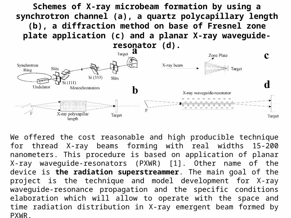
Schemes of X-ray microbeam formation by using a synchrotron channel (a), a quartz polycapillary length (b), a diffraction method on base of Fresnel zone plate application (c) and a planar X-ray waveguide-resonator (d).
We offered the cost reasonable and high producible technique for thread X-ray beams forming with real widths 15-200 nanometers. This procedure is based on application of planar X-ray waveguide-resonators (PXWR) [1]. Other name of the device is the radiation superstreammer. The main goal of the project is the technique and model development for X-ray waveguide-resonance propagation and the specific conditions elaboration which will allow to operate with the space and time radiation distribution in X-ray emergent beam formed by PXWR.[1] V.K. Egorov, E.V. Egorov // Spectrochimica Acta. 2004. Part B59. P. 1049-1069.

Waveguide-resonator as the former of initial X-ray beam for X-ray diffractometry
Positioning the PXWR cell on the conventional X-ray goniometer.
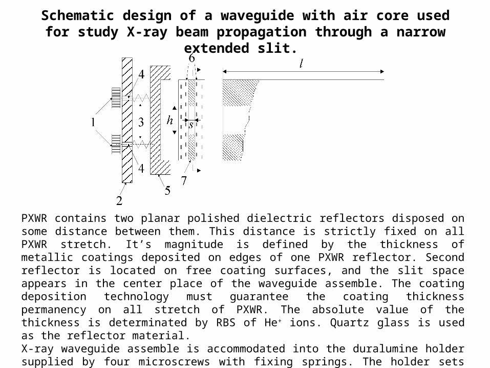
Schematic design of a waveguide with air core used for study X-ray beam propagation through a narrow extended slit.
PXWR contains two planar polished dielectric reflectors disposed on some distance between them. This distance is strictly fixed on all PXWR stretch. It’s magnitude is defined by the thickness of metallic coatings deposited on edges of one PXWR reflector. Second reflector is located on free coating surfaces, and the slit space appears in the center place of the waveguide assemble. The coating deposition technology must guarantee the coating thickness permanency on all stretch of PXWR. The absolute value of the thickness is determinated by RBS of He+ ions. Quartz glass is used as the reflector material.X-ray waveguide assemble is accommodated into the duralumine holder supplied by four microscrews with fixing springs. The holder sets up on the standard X-ray diffractometer instead of the conventional slit-cut former. The holder position is characterized by one translational and two angular degrees of freedom.
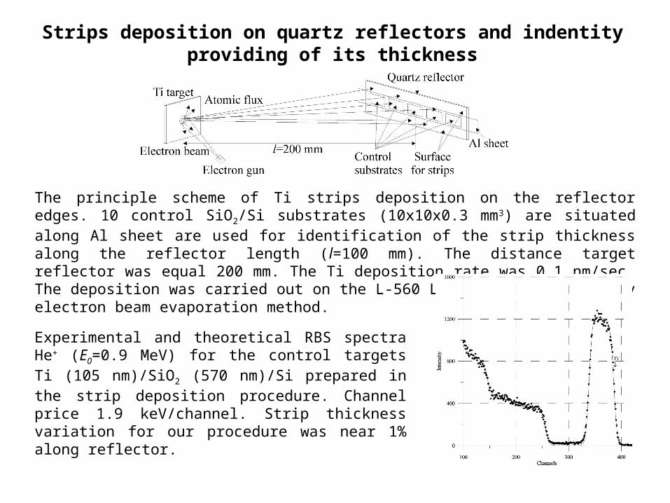
Strips deposition on quartz reflectors and indentity providing of its thickness
The principle scheme of Ti strips deposition on the reflector edges. 10 control SiO2/Si substrates (10x10x0.3 mm3) are situated along Al sheet are used for identification of the strip thickness along the reflector length (l=100 mm). The distance target reflector was equal 200 mm. The Ti deposition rate was 0.1 nm/sec. The deposition was carried out on the L-560 Leybold AG apparatus by electron beam evaporation method.
Experimental and theoretical RBS spectra He+ (E0=0.9 MeV) for the control targets Ti (105 nm)/SiO2 (570 nm)/Si prepared in the strip deposition procedure. Channel price 1.9 keV/channel. Strip thickness variation for our procedure was near 1% along reflector.

Geometry measurement and X-ray distribution in beam after waveguide-resonator
Geometry of PXWR testing on X-ray goniometer. Radiation distribution beam formed by waveguide-resonator with and without attenuator (A). Source X-ray tube (Fe), U=20 keV, I=10 mA. S1=0.1 mm, SW=120 nm.
Capture angle is equal to divergence angle of emergent beam. Attenuation factor KA900.
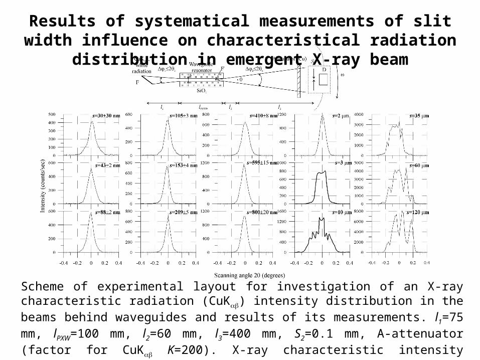
Scheme of experimental layout for investigation of an X-ray characteristic radiation (CuK) intensity distribution in the beams behind waveguides and results of its measurements. l1=75 mm, lPXW=100 mm, l2=60 mm, l3=400 mm, S2=0.1 mm, A-attenuator (factor for CuK K=200). X-ray characteristic intensity distributions collected at the tube (Cu) regime U=20 keV, I=10 mA (b) in beams behind PXWs with different slit widths.
Results of systematical measurements of slit width influence on characteristical radiation distribution in emergent X-ray beam
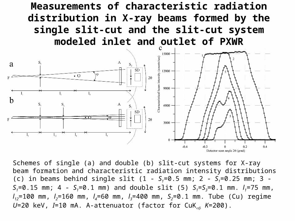
Measurements of characteristic radiation distribution in X-ray beams formed by the single slit-cut and the slit-cut system
modeled inlet and outlet of PXWR
Schemes of single (a) and double (b) slit-cut systems for X-ray beam formation and characteristic radiation intensity distributions (c) in beams behind single slit (1 - S1=0.5 mm; 2 - S1=0.25 mm; 3 - S1=0.15 mm; 4 - S1=0.1 mm) and double slit (5) S1=S3=0.1 mm. l1=75 mm, l12=100 mm, l2=160 mm, l4=60 mm, l3=400 mm, S2=0.1 mm. Tube (Cu) regime U=20 keV, I=10 mA. A-attenuator (factor for CuK K=200).
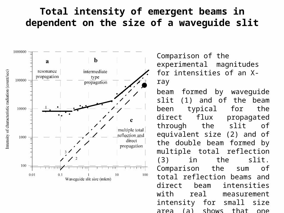
Total intensity of emergent beams in dependent on the size of a waveguide slit
Comparison of the experimental magnitudes for intensities of an X-ray
beam formed by waveguide slit (1) and of the beam been typical for the direct flux propagated through the slit of equivalent size (2) and of the double beam formed by multiple total reflection (3) in the slit. Comparison the sum of total reflection beams and direct beam intensities with real measurement intensity for small size area (a) shows that one must prepose new type of mechanism propagation - resonance manner one.
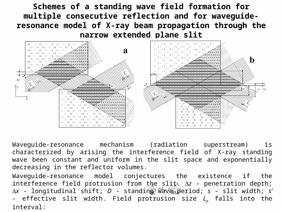
Schemes of a standing wave field formation for multiple consecutive reflection and for waveguide-resonance model of X-ray beam propagation
through the narrow extended plane slit
Waveguide-resonance mechanism (radiation superstream) is characterized by arising the interference field of X-ray standing wave been constant and uniform in the slit space and exponentially decreasing in the reflector volumes.
Waveguide-resonance model conjectures the existence if the interference field protrusion from the slit. z - penetration depth; x - longitudinal shift; D - standing wave period; s - slit width; s’ - effective slit width. Field protrusion size Lp falls into the interval:
2
3
2 82
pc
L
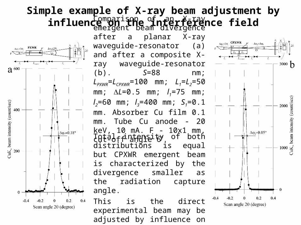
Comparison of an X-ray emergent beam divergence after a planar X-ray waveguide-resonator (a) and after a composite X-ray waveguide-resonator (b). S=88 nm; LPXWR=LCPXWR=100 mm; L1=L2=50 mm; L=0.5 mm; l1=75 mm; l2=60 mm; l3=400 mm; S1=0.1 mm. Absorber Cu film 0.1 mm. Tube Cu anode - 20 keV, 10 mA. F - 10x1 mm, cut-off angle 6.Total intensity of both distributions is equal but CPXWR emergent beam is characterized by the divergence smaller as the radiation capture angle.
This is the direct experimental beam may be adjusted by influence on the interference field of the X-ray standing wave in the PXWR slit.
Simple example of X-ray beam adjustment by influence on the interference field
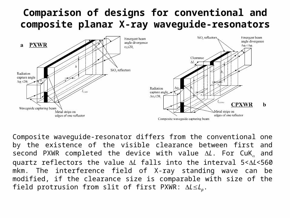
Comparison of designs for conventional and composite planar X-ray waveguide-resonators
Composite waveguide-resonator differs from the conventional one by the existence of the visible clearance between first and second PXWR completed the device with value L. For CuK and quartz reflectors the value L falls into the interval 5<L<560 mkm. The interference field of X-ray standing wave can be modified, if the clearance size is comparable with size of the field protrusion from slit of first PXWR: LLp.
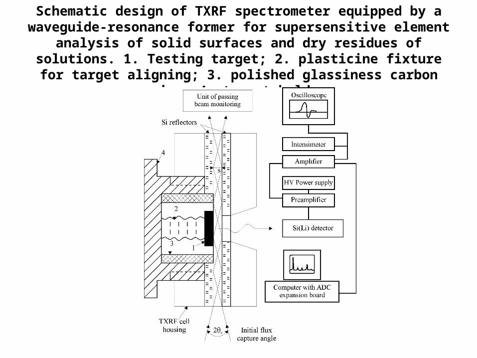
Schematic design of TXRF spectrometer equipped by a waveguide-resonance former for supersensitive element analysis of solid surfaces and dry residues of solutions. 1. Testing target; 2. plasticine fixture for target
aligning; 3. polished glassiness carbon ring; 4. target holder
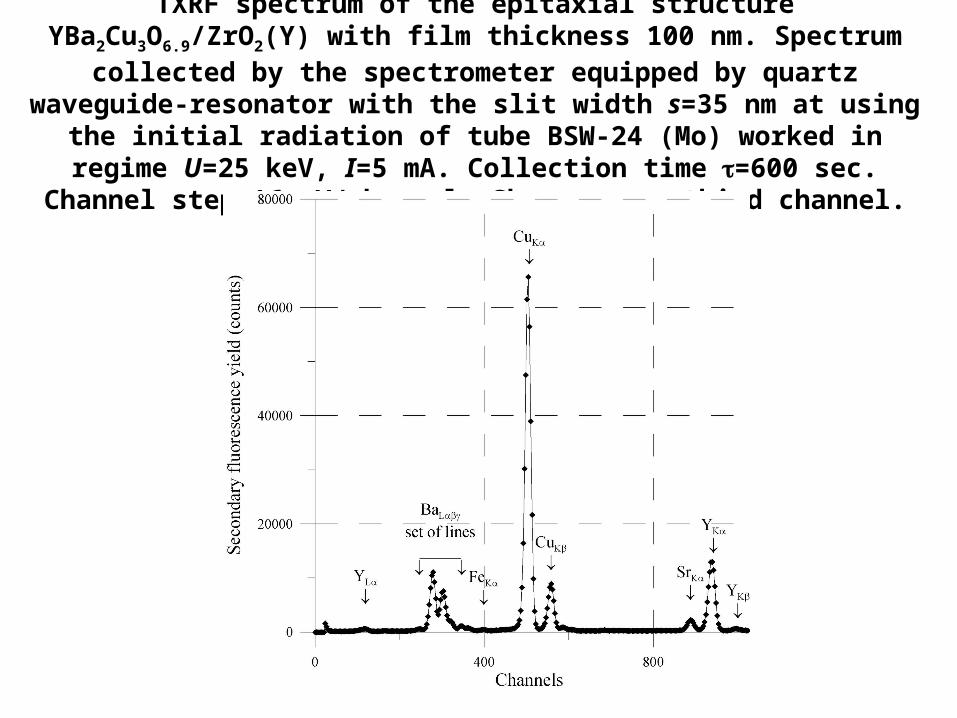
TXRF spectrum of the epitaxial structure YBa2Cu3O6.9/ZrO2(Y) with film thickness 100 nm. Spectrum collected by the spectrometer equipped by quartz waveguide-resonator with the slit width s=35 nm at using the initial radiation of tube BSW-24 (Mo) worked in regime U=25 keV, I=5 mA. Collection time
=600 sec. Channel step 16 eV/channel. Shown every third channel.
Related Documents