4.1 ASynchronous Sequential Circuits ASYNCHRONOUS SEQUENTIAL CIRCUITS UNIT 4 Analysis of asynchronous sequential machines, state assignment, asynchronous design problem 4.1 INTRODUCTION A sequential circuit is specified by a time sequence of inputs, outputs and internal states. In synchronous sequential circuits, the output changes whenever a clock pulse is applied. The memory elements are clocked flip-flops. Asynchronous sequential circuits do not use clock pulses. The memory elements in asynchronous sequential circuits are either unclocked flip-flops (Latches) or time-delay elements. S.No Synchronous sequential circuits Asynchronous sequential circuits 1 Memory elements are clocked flip- flops Memory elements are either unclocked flip-flops or time delay elements. 2 The change in input signals can affect memory element upon activation of clock signal. The change in input signals can affect memory element at any instant of time. 3 The maximum operating speed of clock depends on time delays involved. Therefore synchronous circuits can operate slower than asynchronous. Because of the absence of clock, it can operate faster than synchronous circuits. 4 Easier to design More difficult to design

Welcome message from author
This document is posted to help you gain knowledge. Please leave a comment to let me know what you think about it! Share it to your friends and learn new things together.
Transcript

4.1 ASynchronous Sequential Circuits
ASYNCHRONOUS SEQUENTIAL CIRCUITS
UNIT 4
Analysis of asynchronous sequential machines, state assignment, asynchronous design problem
4.1 INTRODUCTION
A sequential circuit is specified by a time sequence of inputs, outputs and
internal states. In synchronous sequential circuits, the output changes whenever a
clock pulse is applied. The memory elements are clocked flip-flops.
Asynchronous sequential circuits do not use clock pulses. The memory
elements in asynchronous sequential circuits are either unclocked flip-flops (Latches)
or time-delay elements.
S.No Synchronous sequential circuits Asynchronous sequential circuits
1
Memory elements are clocked flip-
flops
Memory elements are either
unclocked flip-flops or time delay
elements.
2
The change in input signals can
affect memory element upon
activation of clock signal.
The change in input signals can
affect memory element at any
instant of time.
3
The maximum operating speed of
clock depends on time delays
involved. Therefore synchronous
circuits can operate slower than
asynchronous.
Because of the absence of clock, it
can operate faster than synchronous
circuits.
4 Easier to design More difficult to design

4.2 ASynchronous Sequential Circuits
Block diagram of Asynchronous sequential circuits
The block diagram of asynchronous sequential circuit is shown above. It
consists of a combinational circuit and delay elements connected to form feedback
loops. There are ‘n’ input variables, ‘m’ output variables, and ‘k’ internal states.
The delay elements provide short term memory for the sequential circuit. The
present-state and next-state variables in asynchronous sequential circuits are called
secondary variables and excitation variables, respectively.
When an input variable changes in value, the ‘y’ secondary variable does not
change instantaneously. It takes a certain amount of time for the signal to propagate
from the input terminals through the combinational circuit to the ‘Y’ excitation
variables where the new values are generated for the next state. These values
propagate through the delay elements and become the new present state for the
secondary variables.
In steady-state condition, excitation and secondary variables are same, but
during transition they are different.
To ensure proper operation, it is necessary for asynchronous sequential
circuits to attain a stable state before the input is changed to a new value. Because of
unequal delays in wires and combinational circuits, it is impossible to have two or

4.3 ASynchronous Sequential Circuits
more input variable change at exactly same instant. Therefore, simultaneous changes
of two or more input variables are avoided.
Only one input variable is allowed to change at any one time and the time
between input changes is kept longer than the time it takes the circuit to reach stable
state.
Types:
According to how input variables are to be considered, there are two types
Fundamental mode circuit
Pulse mode circuit.
Fundamental mode circuit assumes that:
The input variables change only when the circuit is stable.
Only one input variable can change at a given time.
Inputs are levels (0, 1) and not pulses.
Pulse mode circuit assumes that:
The input variables are pulses (True, False) instead of levels.
The width of the pulses is long enough for the circuit to respond to the input.
The pulse width must not be so long that it is still present after the new state
is reached.
4.2 Analysis of Fundamental Mode Circuits
The analysis of asynchronous sequential circuits consists of obtaining a table
or a diagram that describes the sequence of internal states and outputs as a function
of changes in the input variables.
4.4 ASynchronous Sequential Circuits
4.2.1 Analysis procedure
The procedure for obtaining a transition table from the given circuit diagram
is as follows.
1. Determine all feedback loops in the circuit.
2. Designate the output of each feedback loop with variable Y1 and its
corresponding inputs y1, y2,….yk, where k is the number of feedback loops in
the circuit.
3. Derive the Boolean functions of all Y’s as a function of the external inputs and
the y’s.
4. Plot each Y function in a map, using y variables for the rows and the external
inputs for the columns.
5. Combine all the maps into one table showing the value of Y= Y1, Y2,….Yk
inside each square.
6. Circle all stable states where Y=y. The resulting map is the transition table.
4.2.2 Problems
1. An asynchronous sequential circuit is described by the following excitation and
output function,
Y= x1x2+ (x1+x2) y
Z= Y
a) Draw the logic diagram of the circuit.
b) Derive the transition table, flow table and output map.
c) Describe the behavior of the circuit.
Soln:
i) The logic diagram is shown as,
Logic diagram

4.5 ASynchronous Sequential Circuits
ii)
y x1 x2 x1x2 (x1+x2)y Y= x1x2+ (x1+x2)y Z= Y
0
0
0
0
0
0
1
1
0
1
0
1
0
0
0
1
0
0
0
0
0
0
0
1
0
0
0
1
1
1
1
1
0
0
1
1
0
1
0
1
0
0
0
1
0
1
1
1
0
1
1
1
0
1
1
1
Transition table:
Output map:
Output is mapped for all stable states. For unstable states output is mapped
unspecified.
Flow table:
Assign a= 0; b= 1
iii)
The circuit gives carry output of the full adder circuit.

4.6 ASynchronous Sequential Circuits
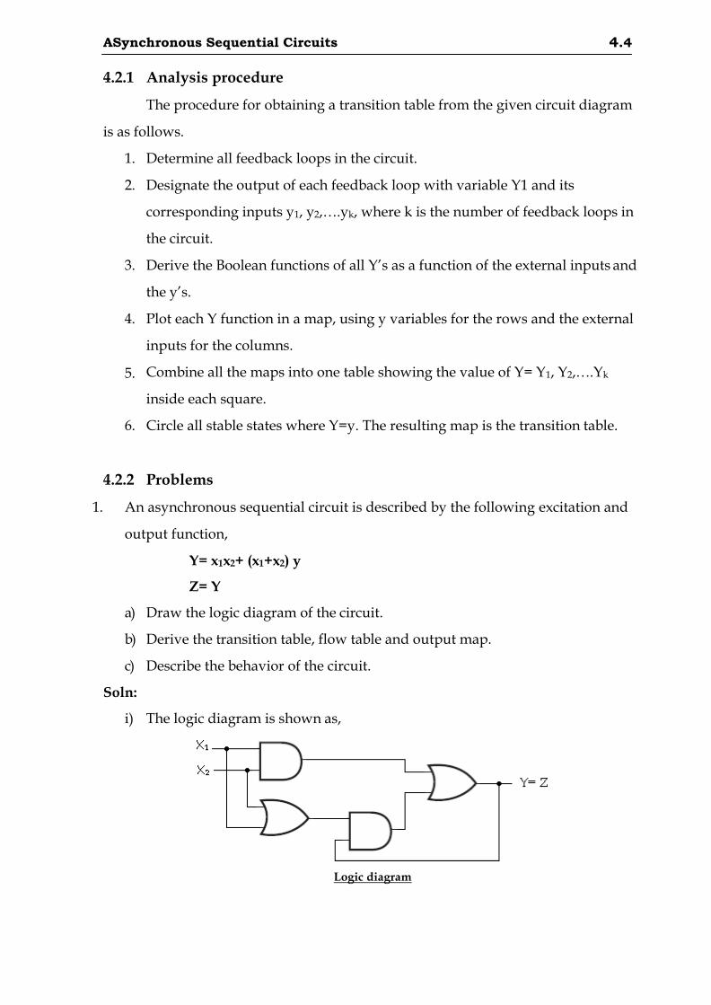
2. Design an asynchronous sequential circuit that has two internal states and one
output. The excitation and output function describing the circuit are as follows:
Y1= x1x2+ x1y2+ x2y1
Y2= x2+ x1y1y2+ x1y1
Z= x2+ y1.
a) Draw the logic diagram of the circuit.
b) Derive the transition table, output map and flow table.
Soln:
i) The logic diagram is shown as,
Logic Diagram
ii)
y1
y2
x1
x2
x1x
2
x1y
2
x2y
1
x1y
1y
2
x1y
1
Y1
Y2
Z=
x2+
y1
0
0
0
0
0
0
0
0
0
0
1
1
0
1
0
1
0
0
0
1
0
0
0
0
0
0
0
0
0
0
0
0
0
0
0
0
0
0
0
1
0
1
0
1
0
1
0
1
4.7 ASynchronous Sequential Circuits
0
0
0
0
1
1
1
1
0
0
1
1
0
1
0
1
0
0
0
1
0
0
1
1
0
0
0
0
0
0
0
0
0
0
0
0
0
0
1
1
0
1
0
1
0
1
0
1
1
1
1
1
0
0
0
0
0
0
1
1
0
1
0
1
0
0
0
1
0
0
0
0
0
1
0
1
0
0
0
0
0
0
1
1
0
1
0
1
0
1
1
1
1
1
1
1
1
1
1
1
1
1
1
1
0
0
1
1
0
1
0
1
0
0
0
1
0
0
1
1
0
1
0
1
0
0
1
1
0
0
1
1
0
1
1
1
0
1
1
1
1
1
1
1
Transition table and Output map
Transition table Output map

4.8 ASynchronous Sequential Circuits
Primitive Flow table
3. An asynchronous sequential circuit is described by the excitation and output
functions,
Y= x1x2’+ (x1+x2’) y
Z= Y
a) Draw the logic diagram of the circuit.
b) Derive the transition table, output map and flow table.
Soln:
Logic diagram
ii)
y x1 x2 x2’ x1x2’ (x1+x2’)y Y= x1x2’+ (x1+x2’)y Z= Y
0
0
0
0
0
0
1
1
0
1
0
1
1
0
1
0
0
0
1
0
0
0
0
0
0
0
1
0
0
0
1
0
1
1
1
1
0
0
1
1
0
1
0
1
1
0
1
0
0
0
1
0
1
0
1
1
1
0
1
1
1
0
1
1

4.9 ASynchronous Sequential Circuits
Transition table:
Output map:
Transition Table
Output is mapped for all stable states. For unstable states output is mapped
unspecified.
Output map
Flow table:
Assign a= 0; b= 1
4. An asynchronous sequential circuit is described by the excitation and output
functions, B= (A1’B2) b+ (A1+B2) C= B
a) Draw the logic diagram of the circuit.
b) Derive the transition table, output map and flow table.
Soln:
Logic Diagram
ii)

4.10 ASynchronous Sequential Circuits
b A1 B2 A1’ (A1’B2)b A1+B2 B= (A1’B2) b+ (A1+B2) C= B
0
0
0
0
0
0
1
1
0
1
0
1
1
1
0
0
0
0
0
0
0
1
1
1
0
1
1
1
0
1
1
1
1
1
1
1
0
0
1
1
0
1
0
1
1
1
0
0
0
1
0
0
0
1
1
1
0
1
1
1
0
1
1
1
Transition table
Output map
Output is mapped for all stable states.
Flow table
Assign a= 0; b= 1

4.11 ASynchronous Sequential Circuits
5. An asynchronous sequential circuit is described by the excitation and output
functions,
X= (Y1Z1’W2) x + (Y1’Z1W2’)
S=X’
a) Draw the logic diagram of the circuit
b) Derive the translation table and output map
Soln:
x
W2
W2’
Y1
Y1’
Z1
Z1’
(Y1Z
1’W
2)
x
Y1’Z
1W
2’
X
S=
X’
0
0
0
0
0
0
0
0
1
1
1
1
0
0
1
1
1
1
0
0
0
1
0
1
1
0
1
0
0
0
0
0
0
1
0
0
0
1
0
0
1
0
1
1
0
0
0
0
1
1
1
1
0
0
0
0
0
0
1
1
1
1
0
0
0
1
0
1
1
0
1
0
0
0
0
0
0
0
0
0
0
0
0
0
1
1
1
1
1
1
1
1
0
0
0
0
1
1
1
1
0
0
1
1
1
1
0
0
0
1
0
1
1
0
1
0
0
0
0
0
0
1
0
0
0
1
0
0
1
0
1
1

4.12 ASynchronous Sequential Circuits
1
1
1
1
1
1
1
1
0
0
0
0
0
0
1
1
1
1
0
0
0
1
0
1
1
0
1
0
0
0
1
0
0
0
0
0
0
0
1
0
1
1
0
1
Transition table and Output map:
Transition table Output map
4.3 Analysis of Pulse Mode Circuits
Pulse mode asynchronous sequential circuits rely on the input pulses rather
than levels. They allow only one input variable to change at a time. They can be
implemented by employing a SR latch.
The procedure for analyzing an asynchronous sequential circuit with SR
latches can be summarized as follows:

4.13 ASynchronous Sequential Circuits
1. Label each latch output with Yi and its external feedback path (if any) with yi
for
i = 1,2 ,..,, k.
2. Derive the Boolean functions for the Si and Ri inputs in each latch.
3. Check whether SR = 0 for each NOR latch or whether S'R' = 0 for each NAND
latch. If either of these condition is not satisfied, there is a possibility that the
circuit may not operate properly.
4. Evaluate Y = S + R’y for each NOR latch or Y = S' + Ry for each NAND latch.
5. Construct a map with the y’s representing the rows and the x inputs
representing the columns.
6. Plot the value of Y= Y1Y2 ……Yk in the map.
7. Circle all stable states such that Y = y. The resulting map is the transition
table.
The analysis of a circuit with latches will be demonstrated by means of the below
example.
1. Derive the transition table for the pulse mode asynchronous sequential circuit
shown below.
Example of a circuit with SR latches

4.14 ASynchronous Sequential Circuits
Soln:
There are two inputs x1 and x2 and two external feedback loops giving rise to
the secondary variables y1 and y2.
Step 1:
The Boolean functions for the S and R inputs in each latch are:
S1= x1y2 S2= x1x2
R1= x1’x2’ R2= x2’y1
Step 2:
Check whether the conditions SR= 0 is satisfied to ensure proper operation of the
circuit.
S1R1= x1y2 x1’x2’ = 0
S2R2= x1x2 x2’y1 = 0
The result is 0 because x1x1’ = x2x2’ = 0
Step 3:
Evaluate Y1 and Y2. The excitation functions are derived from the relation Y= S+ R’y.
Y1= S1+ R1’y1 = x1y2 +(x1’x2’)’ y1
= x1y2 +(x1+ x2) y1 = x1y2 +x1y1+ x2y1
Y2= S2+ R2’y2 = x1x2+ (x2’y1)’y2
= x1x2+ (x2+ y1’) y2 = x1x2+ x2y2+ y1’y2
y1 y2 x1 x2 x1y2 x1y1 x2y1 x1x2 x2y2 y1’y2 Y1 Y2
0
0
0
0
0
0
0
0
0
0
1
1
0
1
0
1
0
0
0
0
0
0
0
0
0
0
0
0
0
0
0
1
0
0
0
0
0
0
0
0
0
0
0
0
0
0
0
1
0
0
0
0
1
1
1
1
0
0
1
1
0
1
0
1
0
0
1
1
0
0
0
0
0
0
0
0
0
0
0
1
0
1
0
1
1
1
1
1
0
0
1
1
1
1
1
1
1
1
0
0
0
0
0
1
0
0
0
0
0
1
0
0
0
0
0
0
0
1
0
0

4.15 ASynchronous Sequential Circuits
1
1
0
0
1
1
0
1
0
0
1
1
0
1
0
1
0
0
0
0
1
1
0
1
1
1
1
1
1
1
1
1
0
0
1
1
0
1
0
1
0
0
1
1
0
0
1
1
0
1
0
1
0
0
0
1
0
1
0
1
0
0
0
0
0
1
1
1
0
1
0
1
Step 4:
Step 5:
Maps for Y1 and Y2.
Transition table

4.16 ASynchronous Sequential Circuits
4.4 RACES:
A race condition is said to exist in an asynchronous sequential circuit when
two or more binary state variables change value in response to a change in an input
variable.
Races are classified as:
i. Non-critical races
ii. Critical races.
Non-critical races:
If the final stable state that the circuit reaches does not depend on the order in
which the state variables change, the race is called a non-critical race.
If a circuit, whose transition table (a) starts with the total stable state y1y2x=
000 and then change the input from 0 to 1. The state variables must then change from
00 to 11, which define a race condition.
The possible transitions are:
00 11
00 01 11
00 10 11
In all cases, the final state is the same, which results in a non-critical condition. In (a),
the final state is (y1y2x= 111), and in (b), it is (y1y2x= 011).
Examples of Non-critical Races

4.17 ASynchronous Sequential Circuits
Critical races:
A race becomes critical if the correct next state is not reached during a state
transition. If it is possible to end up in two or more different stable states, depending
on the order in which the state variables change, then it is a critical race. For proper
operation, critical races must be avoided.
The below transition table illustrates critical race condition. The transition
table (a) starts in stable state (y1y2x= 000), and then change the input from 0 to 1. The
state variables must then change from 00 to 11. If they change simultaneously, the
final total stable state is 111. In the transition table (a), if, because of unequal
propagation delay, Y2 changes to 1 before Y1 does, then the circuit goes to the total
stable state 011 and remains there. If, however, Y1 changes first, the internal state
becomes 10 and the circuit will remain in the stable total state 101.
Hence, the race is critical because the circuit goes to different stable states,
depending on the order in which the state variables change.
Examples of Critical Races
4.5 CYCLES
Races can be avoided by directing the circuit through intermediate unstable
states with a unique state-variable change. When a circuit goes through a unique
sequence of unstable states, it is said to have a cycle.

4.18 ASynchronous Sequential Circuits
Again, we start with y1y2 = 00 and change the input from 0 to 1. The transition
table (a) gives a unique sequence that terminates in a total stable state 101. The table
in (b) shows that even though the state variables change from 00 to 11, the cycle
provides a unique transition from 00 to 01 and then to 11, Care must be taken when
using a cycle that terminates with a stable state. If a cycle does not terminate with a
stable state, the circuit will keep going from one unstable state to another, making
the entire circuit unstable. This is demonstrated in the transition table (c).
Debounce Circuit:
Examples of Cycles
Input binary information in binary information can be generated manually be
means of mechanical switches. One position of the switch provides a voltage
equivalent to logic 1, and the other position provides a second voltage equivalent to
logic 0. Mechanical switches are also used to start, stop, or reset the digital system. A
common characteristic of a mechanical switch is that when the arm is thrown from
one position to the other the switch contact vibrates or bounces several times before
coming to a final rest. In a typical switch, the contact bounce may take several
milliseconds to die out, causing the signal to oscillate between 1 and 0 because the
switch contact is vibrating.
A debounce circuit is a circuit which removes the series of pulses that result
from a contact bounce and produces a single smooth transition of the binary signal
from 0 to 1 or from 1 to 0. One such circuit consists of a single-pole, double-throw
switch connected to an SR latch, as shown below. The center contact is connected to

4.19 ASynchronous Sequential Circuits
ground that provides a signal equivalent to logic 0. When one of the two contacts, A
or B, is not connected to ground through the switch, it behaves like a logic-1 signal.
When the switch is thrown from position A to position B and back, the outputs of the
latch produce a single pulse as shown, negative for Q and positive for Q'. The switch
is usually a push button whose contact rests in position A. When the pushbutton is
depressed, it goes to position B and when released, it returns to position A.
Debounce Circuit
The operation of the debounce circuit is as follows: When the switch resets in
position A, we have the condition S = 0, R = 1 and Q = 1, Q' = 0. When the switch is
moved to position B, the ground connection causes R to go to 0, while S becomes a 1
because contact A is open. This condition in turn causes output Q to go to 0 and Q' to
go to 1. After the switch makes an initial contact with B, it bounces several times. The
output of the latch will be unaffected by the contact bounce because Q' remains 1
(and Q remains 0) whether R is equal to 0 (contact with ground) or equal to 1 (no
contact with ground). When the switch returns to position A, S becomes 0 and Q
returns to 1. The output again will exhibit a smooth transition, even if there is a
contact bounce in position A.

4.20 ASynchronous Sequential Circuits
4.6 DESIGN OF FUNDAMENTAL MODE SEQUENTIAL CIRCUITS
The design of an asynchronous sequential circuit starts from the statement of
the problem and concludes in a logic diagram. There are a number of design steps
that must be carried out in order to minimize the circuit complexity and to produce a
stable circuit without critical races.
The design steps are as follows:
1. State the design specifications.
2. Obtain a primitive flow table from the given design specifications.
3. Reduce the flow table by merging rows in the primitive flow table.
4. Assign binary state variables to each row of the reduced flow table to obtain
the transition table. The procedure of state assignment eliminates any possible
critical races.
5. Assign output values to the dashes associated with the unstable states to
obtain the output maps.
6. Simplify the Boolean functions of the excitation and output variables and
draw the logic diagram.
1. Design a gated latch circuit with inputs, G (gate) and D (data), and one output, Q.
Binary information present at the D input is transferred to the Q output when G
is equal to 1. The Q output will follow the D input as long as G= 1. When G goes
to 0, the information that was present at the D input at the time of transition
occurred is retained at the Q output. The gated latch is a memory element that
accepts the value of D when G= 1 and retains this value after G goes to 0, a
change in D does not change the value of the output Q.
Soln:
Step 1:
From the design specifications, we know that Q= 0 if DG= 01
and Q= 1 if DG= 11
because D must be equal to Q when G= 1.
When G goes to 0, the output depends on the last value of D. Thus, if the
transition is from 01 to 00 to 10, then Q must remain 0 because D is 0 at the time of
the transition from 1 to 0 in G.

4.21 ASynchronous Sequential Circuits
If the transition of DG is from 11 to 10 to 00, then Q must remain 1. This
information results in six different total states, as shown in the table.
State Inputs Output
Comments D G Q
a 0 1 0 D= Q because G= 1
b 1 1 1 D= Q because G= 1
c 0 0 0 After state a or d
d 1 0 0 After state c
e 1 0 1 After state b or f
f 0 0 1 After state e
Step 2: A primitive flow is a flow table with only one stable total state in each
row. It has one row for each state and one column for each input combination.
Step 3:
Primitive flow table
The primitive flow table has only stable state in each row. The table can be
reduced to a smaller number of rows if two or more stable states are placed in the
same row of the flow table. The grouping of stable states from separate rows into
one common row is called merging.

4.22 ASynchronous Sequential Circuits
States that are candidates for merging
Thus, the three rows a, c, and d can be merged into one row. The second row
of the reduced table results from the merging of rows b, e, and f of the primitive flow
table.
Reduced table- 1
The states c & d are replaced by state a, and states e & f are replaced by state b
Step 4:
Reduced table- 2
Assign distinct binary value to each state. This assignment converts the flow
table into a transition table. A binary state assignment must be made to ensure that
the circuit will be free of critical races.
Assign 0 to state a, and 1 to state b in the reduced state table.
Transition table and output map

4.23 ASynchronous Sequential Circuits
Step 5:
Gated-Latch Logic diagram
The diagram can be implemented also by means of an SR latch. Obtain the
Boolean function for S and R inputs.
y Y S R
0 0 1 1
0 1 0 1
0 1 0 x
x 0
1 0
SR Latch excitation table
From the information given in the transition table and from the latch
excitation table conditions, we can obtain the maps for the S and R inputs of the
latch.
Maps for S and R
The logic diagram consists of an SR latch using NOR latch and the gates
required to implement the S and R Boolean functions. With a NAND latch, we must
use the complemented values for S and R.
S’ = (DG)’ and R’ = (D’G)’

4.24 ASynchronous Sequential Circuits
Logic diagram with NOR latch Logic diagram with NAND latch
2. Design a negative-edge triggered T flip-flop. The circuit has two inputs, T
(toggle) and G (clock), and one output, Q. the output state is complemented if T=
1 and the clock changes from 1 to 0 (negative-edge triggering). Otherwise, under
any other input condition, the output Q remains unchanged.
Step 1:
Starting with the input condition TC= 11 and assign it to a. The circuit goes to
state b and output Q complements from 0 to 1 when C changes from 1 to 0 while T
remains a 1.
Another change in the output occurs when the circuit changes from state c to
state d. In this case, T=1, C changes from 1 to 0, and the output Q complements from
1 to 0. The other four states in the table do not change the output, because T is equal
to 0. If Q is initially 0, it stays at 0, and if initially at 1, it stays at 1 even though the
clock input changes.
State Inputs Output
Comments T G Q
a 1 1 0 Initial output is 0
b 1 0 1 After state a
c 1 1 1 Initial output is 1
d 1 0 0 After state c
e 0 0 0 After state d or f
f 0 1 0 After state e or a
g 0 0 1 After state b or h
h 0 1 1 After state g or c Specifications of total states

4.25 ASynchronous Sequential Circuits
Step 2: Merging of the flow table
The information for the primitive flow table can be obtained directly from the
condition listed in the above table. We first fill in one square in each row belonging
to stable state in that row as listed in the table.
Then we enter dashes in those squares whose input differs by two variables
from the input corresponding to the stable state.
The unstable conditions are then determined by utilizing the information
listed under the comments in the above table.
Step 3: Compatible pairs
Primitive flow table
The rows in the primitive flow table are merged by first obtaining all
compatible pairs of states. This is done by means of the implication table.

4.26 ASynchronous Sequential Circuits
Implication table
The implication table is used to find the compatible states. The only difference
is that when comparing rows, we are at liberty to adjust the dashes to fit any desired
condition. The two states are compatible if in every column of the corresponding
rows in the primitive flow table, there are identical or compatible pairs and if there is
no conflict in the output values.
A check mark ( ) designates a square whose pair of states is compatible.
Those states that are not compatible are marked with a cross (x). The remaining
squares are recorded with the implied pairs that need further investigation.
The squares that contain the check marks define the compatible pairs:
(a, f) (b, g) (b, h) (c, h) (d, e) (d, f) (e, f) (g, h)
Step 4: Maximal compatibles
Having found all the compatible pairs, the next step is to find larger set of
states that are compatible. The maximal compatible is a group of compatibles that
contain all the possible combinations of compatible states. The maximal compatible
can be obtained from a merger diagram.

4.27 ASynchronous Sequential Circuits
The merger diagram is a graph in which each state is represented by a dot
placed along the circumference of a circle. Lines are drawn between any two
corresponding dots that form a compatible pair. All possible compatibles can be
obtained from the merger diagram by observing the geometrical patterns in which
states are connected to each other.
A line represents a compatible pair
A triangle constitutes a compatible with three states
An n-state compatible is represented in the merger diagram by an n-sided
polygon with all its diagonals connected.
Merger Diagram
The merger diagram is obtained from the list of compatible pairs derived
from the implication table. There are eight straight lines connecting the dots, one for
each compatible pair. The lines form a geometrical pattern consisting of two
triangles connecting (b, g, h) & (d, e, f) and two lines (a, f) & (c, h). The maximal
compatibles are:
(a, f) (b, g, h) (c, h) (d, e, f)
Reduced Flow table

4.28 ASynchronous Sequential Circuits
The reduced flow table is drawn. The compatible states are merged into one
row that retains the original letter symbols of the states. The four compatible set of
states are used to merge the flow table into four rows.
Final Reduced Flow table
Here we assign a common letter symbol to all the stable states in each merged
row. Thus, the symbol f is replaced by a; g & h are replaced by b, and similarly for
the other two rows.
Step 5: State Assignment and Transition table
Find the race-free binary assignment for the four stable states in the reduced
flow table. Assign a= 00, b= 01, c= 11 and d= 10.
Substituting the binary assignment into the reduced flow table, the transition
table is obtained. The output map is obtained from the reduced flow table.
Transition Table and Output Map
Transition table Output map Q= y2

4.29 ASynchronous Sequential Circuits
Logic Diagram:
Maps for Latch Inputs

4.30 ASynchronous Sequential Circuits
3. Develop a state diagram and primitive flow table for a logic system that has two
inputs, X and Y, and a single output X, which is to behave in the following
manner. Initially, both inputs and output are equal to 0. Whenever X= 1 and Y=
0, the Z becomes 1 and whenever X= 0 and Y= 1, the Z becomes 0. When inputs
are zero, i.e. X= Y= 0 or inputs are one, i.e. X= Y= 1, the output Z does not
change; it remains in the previous state. The logic system has edge triggered
inputs without having a clock. The logic system changes state on the rising edges
of the two inputs. Static input values are not to have any effect in changing the Z
output.
Soln:
The conditions given are,
Initially both inputs X and Y are 0.
When X= 1, Y= 0; Z= 1
When X= 0, Y= 1; Z= 0
When X= Y= 0 or X= Y= 1, then Z does not change, it remains in the previous
state.
Step 1:
The above state transitions are represented in the state diagram as,
State diagram

4.31 ASynchronous Sequential Circuits
Step 2:
A primitive flow table is constructed from the state diagram. The primitive
flow table has one row for each state and one column for each input combination.
Only one stable state exists for each row in the table. The stable state can be easily
identified from the state diagram. For example, state A is stable with output 0 when
inputs are 00, state C is stable with output 1 when inputs are 10 and so on.
We know that both inputs are not allowed to change simultaneously, so we
can enter dash marks in each row that differs in two or more variables from the
input variables associated with the stable state. For example, the first row in the flow
table shows a stable state with an input of 00. Since only one input can change at any
given time, it can change to 01 or 10, but not to 11. Therefore we can enter two
dashes in the 11 column of row A.
The remaining places in the primitive flow table can be filled by observing
state diagram. For example, state B is the next state for present state A when input
combination is 01; similarly state C is the next state for present state A when input
combination is 10.
Step 3:
Primitive flow table
The rows in the primitive flow table are merged by first obtaining all
compatible pairs of states. This is done by means of the implication table.
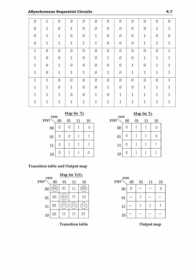
4.32 ASynchronous Sequential Circuits
The squares that contain the check marks ( ) define the compatible pairs:
(A, B) (A, D) (A, F) (B, D) (C, E) (C, F) (D, E) (E, F)
Step 4:
The merger diagram is obtained from the list of compatible pairs derived
from the implication table. There are eight straight lines connecting the dots, one for
each compatible pair. The lines form a geometrical pattern consisting of two
triangles connecting (A, B, D) & (C, E, F) and two lines (A, F) & (D, E). The maximal
compatibles are:
(A, B, D) (C, E, F) (A, F) (D, E)
Closed covering condition:
Merger diagram
The condition that must be satisfied for merging rows is that the set of chosen
compatibles must cover all the states and must be closed. The set will cover all the
states if it includes all the states of the original state table. The closure condition is

4.33 ASynchronous Sequential Circuits
satisfied if there are no implied states or if the implied states are included within the
set. A closed set of compatibles that covers all the states is called a closed covering.
If we remove (A, F) and (D, E), we are left with a set of two compatibles:
(A, B, D) (C, E, F)
All six states from the primitive flow table are included in this set. Thus, the set
satisfies the covering condition.
The reduced flow table is drawn as below.
Reduced flow table
Here we assign a common letter symbol to all the stable states in each merged
row. Thus, the symbol B & D is replaced by A; E & F are replaced by C.
Step 5:
Find the race-free binary assignment for the four stable states in the reduced
flow table. Assign A= 0 and C= 1
Substituting the binary assignment into the reduced flow table, the transition
table is obtained. The output map is obtained from the reduced flow table.
Transition table and output map

4.34 ASynchronous Sequential Circuits
Step 6:
Gated-Latch Logic diagram
4. Design a circuit with inputs X and Y to give an output Z= 1 when XY= 11 but
only if X becomes 1 before Y, by drawing total state diagram, primitive flow table
and output map in which transient state is included.
Soln:
Step 1:
The state diagram can be drawn as,
State table
Step 2:
A primitive flow table is constructed from the state table as,

4.35 ASynchronous Sequential Circuits
Primitive flow table
Step 3:
The rows in the primitive flow table are merged by first obtaining all
compatible pairs of states. This is done by means of the implication table.
Implication table
The squares that contain the check marks ( ) define the compatible pairs:
(A, B) (A, C) (A, D) (A, E) (B, D) (C, E)
Step 4:
The merger diagram is obtained from the list of compatible pairs derived
from the implication table. There are six straight lines connecting the dots, one for
each compatible pair. The lines form a geometrical pattern consisting of one triangle
connecting (A, B, D) & a line (C, E). The maximal compatibles are:
(A, B, D) (C, E)
4.36 ASynchronous Sequential Circuits
Merger diagram
The reduced flow table is drawn as below.
Reduced flow table
Here we assign a common letter symbol to all the stable states in each merged
row. Thus, the symbol B & D is replaced by A; E is replaced by C.
Transition table
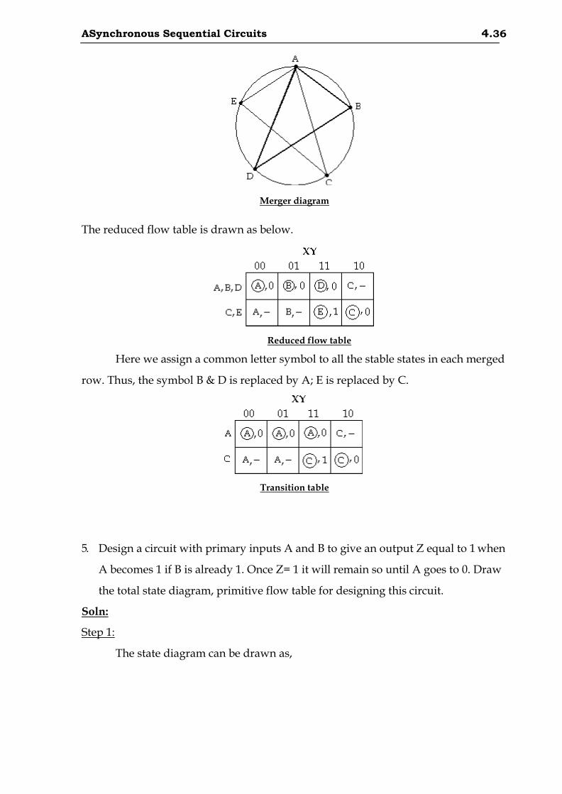
5. Design a circuit with primary inputs A and B to give an output Z equal to 1 when
A becomes 1 if B is already 1. Once Z= 1 it will remain so until A goes to 0. Draw
the total state diagram, primitive flow table for designing this circuit.
Soln:
Step 1:
The state diagram can be drawn as,
4.37 ASynchronous Sequential Circuits
Step 2:
State diagram
A primitive flow table is constructed from the state table as,
Primitive flow table
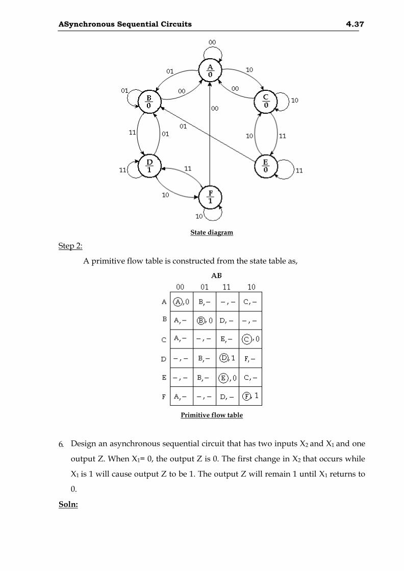
6. Design an asynchronous sequential circuit that has two inputs X2 and X1 and one
output Z. When X1= 0, the output Z is 0. The first change in X2 that occurs while
X1 is 1 will cause output Z to be 1. The output Z will remain 1 until X1 returns to
0.
Soln:

4.38 ASynchronous Sequential Circuits
Step 1:
Step 2:
Step 3:
The state diagram can be drawn as,
State diagram
A primitive flow table is constructed from the state table as,
Primitive flow table
The rows in the primitive flow table are merged by obtaining all compatible
pairs of states. This is done by means of the implication table.

4.39 ASynchronous Sequential Circuits
Implication table
The squares that contain the check marks ( ) define the compatible pairs:
(A, B) (A, C) (C, E) (D, F)
Step 4:
The merger diagram is obtained from the list of compatible pairs derived
from the implication table. There are four straight lines connecting the dots, one for
each compatible pair. It consists of four lines (A, B), (A, C), (C, E) and (D, F).
The maximal compatibles are:
Merger diagram
(A, B) (C, E) (D, F)
This set of maximal compatible covers all the original states resulting in the reduced
flow table.
The reduced flow table is drawn as below.

4.40 ASynchronous Sequential Circuits
Flow table
Here we assign a common letter symbol to all the stable states in each merged
row. Thus, the symbol B is replaced by A; E is replaced by C and F is replaced by D.
Step 5:
Reduced Flow table
Find the race-free binary assignment for the four stable states in the reduced
flow table. Assign A= S0, C= S1 and D= S2.
Now, if we assign S0= 00, S1 = 01 and S2 = 10, then we need one more state S3=
11 to prevent critical race during transition of S0 S1 or S2 S1. By introducing S3
the transitions S1 S2 and S2 S1 are routed through S4.
Thus after state assignment the flow table can be given as,

4.41 ASynchronous Sequential Circuits
Flow table with state assignment
Substituting the binary assignment into the reduced flow table, the transition
table is obtained. The output map is obtained from the reduced flow table.
K- Map simplification:

4.42 ASynchronous Sequential Circuits
Logic Diagram:
7. Obtain a primitive flow table for a circuit with two inputs x1 and x2 and two
outputs z1 and z2 that satisfies the following four conditions.
i. When x1x2 = 00, output z1z2 = 00.
ii. When x1= 1 and x2 changes from 0 to 1, the output z1z2 = 01.
iii. When x2= 1 and x1 changes from 0 to 1, the output z1z2 = 10.
iv. Otherwise the output does not change.
Soln:
The state diagram can be drawn as,
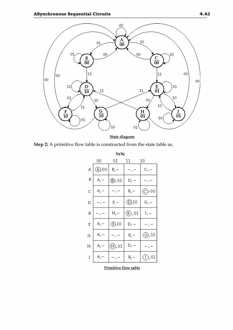
4.43 ASynchronous Sequential Circuits
State diagram
Step 2: A primitive flow table is constructed from the state table as,
Primitive flow table

4.44 ASynchronous Sequential Circuits
4.7 HAZARDS
Hazards are unwanted switching transients that may appear at the output of
a circuit because different paths exhibit different propagation delays.
Hazards occur in combinational circuits, where they may cause a temporary
false-output value. When this condition occurs in asynchronous sequential circuits, it
may result in a transition to a wrong stable state.
Hazards in Combinational Circuits:
A hazard is a condition where a single variable change produces a
momentary output change when no output change should occur.
Types of Hazards:
Static hazard
Dynamic hazard
4.7.1 Static Hazard
In digital systems, there are only two possible outputs, a ‘0’ or a ‘1’. The
hazard may produce a wrong ‘0’ or a wrong ‘1’. Based on these observations, there
are three types,
Static- 0 hazard,
Static- 1 hazard,
Static- 0 hazard:
When the output of the circuit is to remain at 0, and a momentary 1 output is
possible during the transmission between the two inputs, then the hazard is called a
static 0-hazard.
Static- 1 hazard:
When the output of the circuit is to remain at 1, and a momentary 0 output is
possible during the transmission between the two inputs, then the hazard is called a
static 1-hazard.

4.45 ASynchronous Sequential Circuits
The below circuit demonstrates the occurrence of a static 1-hazard. Assume
that all three inputs are initially equal to 1 i.e., X1X2X3= 111. This causes the output of
the gate 1 to be 1, that of gate 2 to be 0, and the output of the circuit to be equal to 1.
Now consider a change of X2 from 1 to 0 i.e., X1X2X3= 101. The output of gate 1
changes to 0 and that of gate 2 changes to 1, leaving the output at 1. The output may
momentarily go to 0 if the propagation delay through the inverter is taken into
consideration.
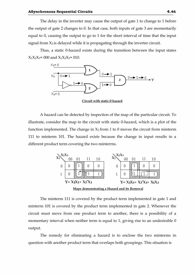
The delay in the inverter may cause the output of gate 1 to change to 0 before
the output of gate 2 changes to 1. In that case, both inputs of gate 3 are momentarily
equal to 0, causing the output to go to 0 for the short interval of time that the input
signal from X2 is delayed while it is propagating through the inverter circuit.
Thus, a static 1-hazard exists during the transition between the input states
X1X2X3= 111 and X1X2X3= 101.
Circuit with static-1 hazard
Now consider the below network, and assume that the inverter has an
appreciably greater propagation delay time than the other gates. In this case there is
a static 0-hazard in the transition between the input states X1X2X3= 000 and X1X2X3=
010 since it is possible for a logic-1 signal to appear at both input terminals of the
AND gate for a short duration.
4.46 ASynchronous Sequential Circuits
The delay in the inverter may cause the output of gate 1 to change to 1 before
the output of gate 2 changes to 0. In that case, both inputs of gate 3 are momentarily
equal to 0, causing the output to go to 1 for the short interval of time that the input
signal from X2 is delayed while it is propagating through the inverter circuit.
Thus, a static 0-hazard exists during the transition between the input states
X1X2X3= 000 and X1X2X3= 010.
Circuit with static-0 hazard
A hazard can be detected by inspection of the map of the particular circuit. To
illustrate, consider the map in the circuit with static 0-hazard, which is a plot of the
function implemented. The change in X2 from 1 to 0 moves the circuit from minterm
111 to minterm 101. The hazard exists because the change in input results in a
different product term covering the two minterrns.
Maps demonstrating a Hazard and its Removal
The minterm 111 is covered by the product term implemented in gate 1 and
minterm 101 is covered by the product term implemented in gate 2. Whenever the
circuit must move from one product term to another, there is a possibility of a
momentary interval when neither term is equal to 1, giving rise to an undesirable 0
output.
The remedy for eliminating a hazard is to enclose the two minterms in
question with another product term that overlaps both groupings. This situation is

4.47 ASynchronous Sequential Circuits
shown in the map above, where the two terms that causes the hazard are combined
into one product term. The hazard- free circuit obtained by this combinational is
shown below.
Hazard-free Circuit
The extra gate in the circuit generates the product term X1X4. The hazards in
combinational circuits can be removed by covering any two minterms that may
produce a hazard with a product term common to both. The removal of hazards
requires the addition of redundant gates to the circuit.
4.7.2 Dynamic Hazard
A dynamic hazard is defined as a transient change occurring three or more
times at an output terminal of a logic network when the output is supposed to
change only once during a transition between two input states differing in the value
of one variable.
Now consider the input states X1X2X3= 000 and X1X2X3= 100. For the first
input state, the steady state output is 0; while for the second input state, the steady
state output is 1. To facilitate the discussion of the transient behavior of this network,
assume there are no propagation delays through gates G3 and G5 and that the
propagation delays of the other three gates are such that G1 can switch faster than G2
and G2 can switch faster than G4.

4.48 ASynchronous Sequential Circuits
Circuit with Dynamic hazard
When X1 changes from 0 to 1, the change propagates through gate G1 before
gate G2 with the net effect that the inputs to gate G3 are simultaneously 1 and the
network output changes from 0 to 1. Then, when X1 change propagates through gate
G2, the lower input to gate G3 becomes 0 and the network output changes back to 0.
Finally, when the X1= 1 signal propagates through gate G4, the lower input to
gate G5 becomes 1 and the network output again changes to 1. It is therefore seen
that during the change of X1 variable from 0 to 1 the output undergoes the sequence,
0 1 0 1, which results in three changes when it should have undergone
only a single change.
4.7.3 Essential Hazard
An essential hazard is caused by unequal delays along two or more paths that
originate from the same input. An excessive delay through an inverter circuit in
comparison to the delay associated with the feedback path may cause such a hazard.
Essential hazards elimination:
Essential hazards can be eliminated by adjusting the amount of delays in the
affected path. To avoid essential hazards, each feedback loop must be handled with
individual care to ensure that the delay in the feedback path is long enough
compared with delays of other signals that originate from the input terminals.

4.49 ASynchronous Sequential Circuits
4.8 Design Of Hazard Free Circuits
1. Design a hazard-free circuit to implement the following function.
F (A, B, C, D) = ∑m (1, 3, 6, 7, 13, 15)
Soln:
a) K-map Implementation and grouping
F=A’B’D+ A’BC+ ABD
b) Hazard- free realization
The first additional product term A’CD, overlapping two groups (group 1 &
2) and the second additional product term, BCD, overlapping the two groups
(group 2 & 3).
F=A’B’D+ A’BC+ ABD+ A’CD+ BCD
2. Design a hazard-free circuit to implement the following function.
F (A, B, C, D) = ∑m (0, 2, 6, 7, 8, 10, 12).
Soln:
a) K-map Implementation and grouping
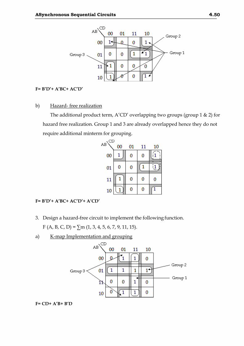
4.50 ASynchronous Sequential Circuits
F= B’D’+ A’BC+ AC’D’
b) Hazard- free realization
The additional product term, A’CD’ overlapping two groups (group 1 & 2) for
hazard free realization. Group 1 and 3 are already overlapped hence they do not
require additional minterm for grouping.
F= B’D’+ A’BC+ AC’D’+ A’CD’
3. Design a hazard-free circuit to implement the following function.
F (A, B, C, D) = ∑m (1, 3, 4, 5, 6, 7, 9, 11, 15).
a) K-map Implementation and grouping
F= CD+ A’B+ B’D

4.51 ASynchronous Sequential Circuits
b) Hazard- free realization
The additional product term, A’D overlapping two groups (group 2 & 3) for
hazard free realization. Group 1 and 2 are already overlapped hence they do not
require additional minterm for grouping.
F= CD+ A’B+ B’D+ A’D
4. Design a hazard-free circuit to implement the following function.
F (A, B, C, D) = ∑m (0, 2, 4, 5, 6, 7, 8, 10, 11, 15).
Soln:
a) K-map Implementation and grouping
F= B’D’+ A’B+ ACD
b) Hazard- free realization

4.52 ASynchronous Sequential Circuits
F= B’D’+ A’B+ ACD+ A’C’D’+ BCD+ AB’C
5. Design a hazard-free circuit to implement the following function.
F (A, B, C, D) = ∑m (0, 1, 5, 6, 7, 9, 11).
a) K-map Implementation and grouping
F= AB’D+ A’BC+ A’BD+ A’B’C’
b ) Hazard- free realization:
F= AB’D+ A’BC+ A’BD+ A’B’C’+ A’C’D+ B’C’D
Related Documents