Bonding configuration and density of defects of SiOxHy thin films deposited by the electron cyclotron resonance plasma method E. San Andrés, A. del Prado, I. Mártil, G. González-Díaz, D. Bravo et al. Citation: J. Appl. Phys. 94, 7462 (2003); doi: 10.1063/1.1626798 View online: http://dx.doi.org/10.1063/1.1626798 View Table of Contents: http://jap.aip.org/resource/1/JAPIAU/v94/i12 Published by the AIP Publishing LLC. Additional information on J. Appl. Phys. Journal Homepage: http://jap.aip.org/ Journal Information: http://jap.aip.org/about/about_the_journal Top downloads: http://jap.aip.org/features/most_downloaded Information for Authors: http://jap.aip.org/authors Downloaded 03 Oct 2013 to 202.116.1.148. This article is copyrighted as indicated in the abstract. Reuse of AIP content is subject to the terms at: http://jap.aip.org/about/rights_and_permissions

Welcome message from author
This document is posted to help you gain knowledge. Please leave a comment to let me know what you think about it! Share it to your friends and learn new things together.
Transcript
Bonding configuration and density of defects of SiOxHy thin films depositedby the electron cyclotron resonance plasma methodE. San Andrés, A. del Prado, I. Mártil, G. González-Díaz, D. Bravo et al. Citation: J. Appl. Phys. 94, 7462 (2003); doi: 10.1063/1.1626798 View online: http://dx.doi.org/10.1063/1.1626798 View Table of Contents: http://jap.aip.org/resource/1/JAPIAU/v94/i12 Published by the AIP Publishing LLC. Additional information on J. Appl. Phys.Journal Homepage: http://jap.aip.org/ Journal Information: http://jap.aip.org/about/about_the_journal Top downloads: http://jap.aip.org/features/most_downloaded Information for Authors: http://jap.aip.org/authors
Downloaded 03 Oct 2013 to 202.116.1.148. This article is copyrighted as indicated in the abstract. Reuse of AIP content is subject to the terms at: http://jap.aip.org/about/rights_and_permissions
JOURNAL OF APPLIED PHYSICS VOLUME 94, NUMBER 12 15 DECEMBER 2003
Bonding configuration and density of defects of SiO xHy thin filmsdeposited by the electron cyclotron resonance plasma method
E. San Andres, A. del Prado, I. Martil,a) and G. Gonzalez-DıazDepartamento de Fı´sica Aplicada III, Facultad Ciencias Fı´sicas, Universidad Complutense,E-28040 Madrid, Spain
D. Bravo and F. J. LopezDepartamento de Fı´sica de Materiales, Facultad de Ciencias, C IV, Universidad Auto´noma de Madrid,E-28049 Madrid, Spain
M. FernandezInstituto de Ciencia de los Materiales, C. S. I. C., E-28049 Cantoblanco, Spain
W. Bohne, J. Rohrich, B. Selle, and I. SieberHahn-Meitner-Institut Berlin, Glienicker Strasse 100, D-14109 Berlin, Germany
~Received 14 May 2003; accepted 22 September 2003!
The composition, bonding configuration, hydrogen content, and paramagnetic defects of SiOxHy
thin films were studied. Films were deposited by the electron cyclotron resonance plasma method atroom temperature using SiH4 and O2 as precursor gases. The film composition was measured byheavy ion elastic recoil detection analysis and energy dispersive x-ray spectroscopy. Suboxide filmswith compositions ranging from SiO2 to SiH0.38 were obtained. Infrared spectroscopy showed thepresence of different Si–O and Si–H vibration modes. The usual estimation of the oxygen to siliconratio by the wave number of the Si–O–Si stretching band was not accurate for films far fromstoichiometry. These off-stoichiometric films also showed a broader Si–O–Sistretching peak thanthe stoichiometric ones, indicating a higher bonding disorder. The position of the Si–O–Sibendingand rocking modes did not depend on the film composition. On the other hand, the peak position ofthe Si–H modes were found strongly dependent on the Si environment. By single-wavelengthellipsometry atl5632.8 nm the refractive indexn was found to range between 1.45 (SiO2) and2.04 (SiO0.06H0.36). Electron spin resonance measurements showed that stoichiometric filmspresented the well knownE8 center ("Si[O3) with concentrations in the 1016– 1017 cm23 range,while for Si-rich films (x!1) the Si dangling bond center (SiDB , "Si[Si3) was the only detectabledefect, with concentrations in the 1018– 1019 cm23 range. In near-stoichiometric films bothE8 andSiDB centers were found. ©2003 American Institute of Physics.@DOI: 10.1063/1.1626798#
gt
O
b-deraefi
n-leol
S-
in
ial
ofateunit
be
h a
OXs, sos.
u-ers,neti-
ndma
I. INTRODUCTION
Si-rich SiOx films ~SROX! have a wide and increasininterest in the field of Si-based device technology dueseveral reasons:
~i! SROX layers are always present at the Si/Si2
interface1 even on thermally grown SiO22 and also on many
high-K dielectric/Si interfaces.3 The presence of these suoxide layers and their characteristics are strongly depenon surface preparation, deposition process, annealing paeters, etc. These suboxides may generate interface dstates which limit the dielectric performance when usedMOS structures.1
~ii ! Recently SROX films have found application in novolatile memory devices, where the use of a stack of dietrics SROX/SiO2 reduces the erasing time and the threshvoltage.4–6
~iii ! Annealed SROX films show the presence ofnanocrystals~nc-Si!.7 Much work is being done on the electroluminescence properties of these nc-Si embedded
a!Author to whom correspondence should be addressed; [email protected]
7460021-8979/2003/94(12)/7462/8/$20.00
Downloaded 03 Oct 2013 to 202.116.1.148. This article is copyrighted as indicated in the abstract.
o
ntm-ectn
c-d
i
a
SiO2 matrix.8,9 This is an interesting issue due to its potentoptoelectronic applications.
~iv! By now, to increase the electrical performanceMOSFET devices there is a constant reduction in glengths. Therefore, higher values of the capacitance perarea of the gate dielectric@Cdiel5(«)/tdiel , where« is thedielectric permittivity andtdiel is the dielectric thickness# arenecessary. With thermally grown silicon dioxide (SiO2) asgate insulator a gate oxide thickness of 2–3 nm willneeded. The problem of using such a thin SiO2 film is theoccurrence of high gate leakage currents. SROX films, withigher permittivity value, between 3.8 (SiO2)10 and 11.9~Si!,11 allow gates thicker than those made of SiO2 with thesame capacitance per unit area. But the problem with SRis its decreasing band gap when the Si content increasethe advantage in permittivity may be lost by gate leakage
Some physical characteristics of SROX films that inflence device performance and reliability are, among oththe high hydrogen content and the presence of paramagcally active defects~e.g., dangling bonds!.12 The hydrogen isbonded in different configurations (Si5H2, SinO32n
[Si–H, etc.!13 depending on the film deposition process ail:
2 © 2003 American Institute of Physics
Reuse of AIP content is subject to the terms at: http://jap.aip.org/about/rights_and_permissions
re
she
in
Xinhith
,
mmg
edron-
tioitiemm
tly
tes
ragporeio
e
h
ete
sy
w
th
tanteitionthetak
as
ex-
en-dexoil
y-
a
srea-
w asa-daythecon-
posi-
hictorndby
inceents
I-
ual
esal
ub-ig-sain
the
uree
7463J. Appl. Phys., Vol. 94, No. 12, 15 December 2003 San Andres et al.
on the suboxide composition. The bonded hydrogen andconfiguration can be detected by Fourier transform infraspectroscopy~FTIR!.14 The dangling bonds~usually para-magnetic! play a key role in the device performance.15 De-pending on the film composition, the dominant defect hadifferent microscopic structure, changing its type from twell knownE8 center ("Si[O3) in stoichiometric SiO2 filmsto the Si-dangling bond defect ("Si[Si3 , in the followingSiDB) in SROX films far from the stoichiometry.16 The studyof defects in SROX films is scarce and few articles dealwith this problem can be found in the literature.12,17
There are many different techniques to grow SROfilms.12,18–20A desirable objective is a low thermal budgetthe growing process. Not all deposition processes fulfill trequirement. Low thermal budget is desirable because ifgate growth process takes place at high temperaturespreceding processes~mainly the implantations! may sufferfrom degradation, resulting in nonfunctional devices. Plasprocesses are able to deposit thin dielectric films at low teperatures in short times, so much effort has been made tofilms with device characteristics from plasma-excitgases.13,21–23This plasma can be generated by different pcedures; among them the electron cyclotron resonaplasma method~in the following ECR! shows various advantages:
~i! It is a remote plasma system due to the separabetween the plasma generation zone and the deposchamber. Then, only neutral atoms and radicals are ablreach the substrate surface. As a consequence any dawhich could be generated by ion bombardment or plasirradiation is significantly reduced.24
~ii ! The degree of activation of species is significansuperior in ECR plasmas than in other plasma methods.25
~iii ! With the ECR plasma method, high quality gadielectrics can be deposited at low deposition temperature26
achieving the objective of the low thermal budget.The aim of this article is to analyze the bonding structu
of SROX films and the type and concentration of paramnetic defects present as a function of the actual film comsition. The analyzed films were deposited at room tempeture by the ECR method. The deposition parameters wadjusted to scan the range of compositions from stoichmetric SiO2 to SiHy .
II. EXPERIMENT
Several series of films were deposited onto a simplifiRadio Corporation of America~RCA! cleaned high-resistivity ~80 V cm! Si~111! substrates polished on botsides. The substrates had dimensions of 131 cm2. The depo-sition processes were carried out at a base pressur631027 mbar in a homemade chamber attached to an As4500 ECR reactor. Further details about the depositiontem are given elsewhere.27 High purity SiH4 and O2 wereused as precursor gases. Films of several compositionsobtained depending on the gas flow ratio, that we definethis article in the same way as Bulkinet al.,18 i.e., asRb5@SiH4#/(@SiH4#1@O2#). In this study,Rb . was varied be-tween 0.2 and 1. For all depositions, the total gas flow,
Downloaded 03 Oct 2013 to 202.116.1.148. This article is copyrighted as indicated in the abstract.
itsd
a
g
se
the
a-et
-ce
nontoagea
,
e--
a-re-
d
ofxs-
erein
e
total pressure and the microwave power were kept consat 10.5 sccm, 9.331024 mbar, and 100 W, respectively. Thsubstrates were not intentionally heated and the depostemperature was in the 50– 60 °C range. The thickness ofdeposited films was about 250 nm, measured with a Dekprofilometer. Low values ofRb ~below 0.4! resulted in sto-ichiometric, almost hydrogen-free SiO2 films, while highervalues~in the 0.6–0.9 range! yielded off-stoichiometric filmswith high hydrogen content. These films will be referredSiOxHy ~with x the oxygen to silicon ratio of the films andythe hydrogen to silicon ratio!. At Rb51 no O2 was intro-duced into the deposition chamber. These films did nothibit oxygen incorporation and will be referred to as SiHy .
The composition, the bonding configuration, the conctration of paramagnetic defects as well as the refractive inof films were obtained by means of heavy ion elastic recdetection analysis~HI-ERDA! and energy dispersive x-raspectroscopy~EDX!, Fourier transform infrared spectroscopy ~FTIR!, electron spin resonance~ESR!, and ellipsomet-ric measurements, respectively.
The HI-ERDA measurements were carried out withmass and energy dispersive time-of-flight~ToF! setup.28 Theions used as projectiles were 230 MeV129Xe ions providedby the ion beam facility~ISL! of the Hahn-Meitner-Institut inBerlin. The detection system with a solid angle of 0.4 mand the use of a large detection angle of 60° provided rsonable measuring statistics, even at ion fluences as lo1012 ions cm22. The number of incident particles was mesured with an accuracy of 2% using a ‘‘transmission Faracup.’’ 29 Some samples showed hydrogen loss duringmeasuring process. To obtain the zero dose hydrogencentration, an effusion model, previously described,30 wasused. These measurements provided the absolute comtion of the samples, i.e., thex and y values of the SiOxHy
formula, without the need of calibration samples.EDX measurements were performed with a Hitac
S-4100 scanning microscope attached to a Si-Q-DetePioneer of NORAN. The acceleration voltage was 5 keV athe takeoff angle was 30°. The correction was calculatedthe Proza method.31 A certified SiO2 stoichiometric layer de-posited by LPCVD was used as a calibration standard. SEDX was not able to detect hydrogen, these measuremprovided only information on thex value. Thex values ob-tained by EDX were very similar to those obtained by HERDA. In the following the averaged value ofx measured byEDX and measured by HI-ERDA will be used as the actoxygen to silicon ratio of the films.
FTIR characterizations were done in th400– 4000 cm21 range with a Nicolet Magna-IR 750 serieII spectrometer working in the transmission mode at normincidence. The spectrum of the film was obtained by stracting the spectrum of a bare-Si sample from the total snal (substrate1deposited film). Additionally, the baselineof the resulting spectra were corrected and, thus, the mcharacteristics were measured. Following articles ofNorth Carolina State University group,13,32 the peak positionof the main Si–O–Sistretching band can be used to measthe oxygen to silicon ratio of the films. We will compar
Reuse of AIP content is subject to the terms at: http://jap.aip.org/about/rights_and_permissions
rel isr tfivthTa
tn
-
e-
ndtenaThu
.ll f
entSU
g
its
er
of
dlo-
i
7464 J. Appl. Phys., Vol. 94, No. 12, 15 December 2003 San Andres et al.
these results with the actualx value obtained by HI-ERDAand by EDX.
ESR characterization was performed at room tempeture with a Bruker ESP 300E spectrometer operating in thband at a microwave power of 0.5 mW. This signal levelow enough to prevent the saturation of the signal. In ordeenhance the ESR signal each film used was cut intopieces of 0.231 cm. These five pieces were stacked, soeffective thickness of each sample was about 1250 nm.density of paramagnetic centers was quantified by compson with the signal of a calibrated weak pitch standard.26
Thinner samples~80 nm thick! were characterized byellipsometry to obtain the refractive indexn of the SiOxHy
films. These measurements were performed with a GaerL116B ellipsometer operated atl5632.8 nm.
III. RESULTS
A. Structural characterization
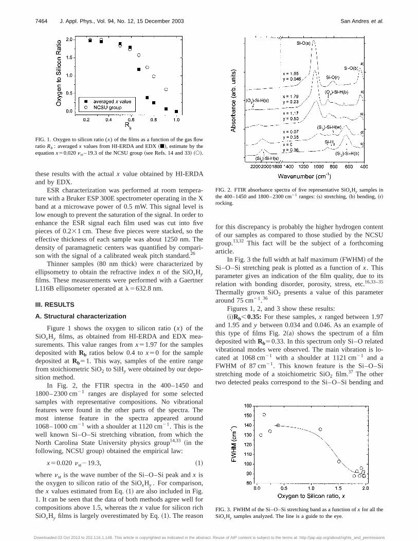
Figure 1 shows the oxygen to silicon ratio (x) of theSiOxHy films, as obtained from HI-ERDA and EDX measurements. This value ranges fromx51.97 for the samplesdeposited withRb ratios below 0.4 tox50 for the sampledeposited atRb51. This way, samples of the entire rangfrom stoichiometric SiO2 to SiHy were obtained by our deposition method.
In Fig. 2, the FTIR spectra in the 400–1450 a1800– 2300 cm21 ranges are displayed for some selecsamples with representative compositions. No vibratiofeatures were found in the other parts of the spectra.most intense feature in the spectra appeared aro1068– 1000 cm21 with a shoulder at 1120 cm21. This is thewell known Si–O–Si stretching vibration, from which theNorth Carolina State University physics group14,33 ~in thefollowing, NCSU group! obtained the empirical law:
x50.020nst219.3, ~1!
wherenst is the wave number of the Si–O–Sipeak andx isthe oxygen to silicon ratio of the SiOxHy . For comparison,thex values estimated from Eq.~1! are also included in Fig1. It can be seen that the data of both methods agree wecompositions above 1.5, whereas thex value for silicon richSiOxHy films is largely overestimated by Eq.~1!. The reason
FIG. 1. Oxygen to silicon ratio (x) of the films as a function of the gas flowratio Rb : averagedx values from HI-ERDA and EDX~j!, estimate by theequationx50.020nst– 19.3 of the NCSU group~see Refs. 14 and 33! ~s!.
Downloaded 03 Oct 2013 to 202.116.1.148. This article is copyrighted as indicated in the abstract.
a-X
oeeheri-
er
dle
nd
or
for this discrepancy is probably the higher hydrogen contof our samples as compared to those studied by the NCgroup.13,32 This fact will be the subject of a forthcominarticle.
In Fig. 3 the full width at half maximum~FWHM! of theSi–O–Sistretching peak is plotted as a function ofx. Thisparameter gives an indication of the film quality, due torelation with bonding disorder, porosity, stress, etc.16,33–35
Thermally grown SiO2 presents a value of this parametaround 75 cm21.36
Figures 1, 2, and 3 show these results:~i!Rb,0.35: For these samples,x ranged between 1.97
and 1.95 andy between 0.034 and 0.046. As an examplethis type of films Fig. 2~a! shows the spectrum of a filmdeposited withRb50.33. In this spectrum only Si–O relatevibrational modes were observed. The main vibration iscated at 1068 cm21 with a shoulder at 1121 cm21 and aFWHM of 87 cm21. This known feature is the Si–O–Sstretching mode of a stoichiometric SiO2 film.37 The othertwo detected peaks correspond to the Si–O–Sibending and
FIG. 2. FTIR absorbance spectra of five representative SiOxHy samples inthe 400–1450 and 1800– 2300 cm21 ranges:~s! stretching,~b! bending,~r!rocking.
FIG. 3. FWHM of the Si–O–Sistretching band as a function ofx for all theSiOxHy samples analyzed. The line is a guide to the eye.
Reuse of AIP content is subject to the terms at: http://jap.aip.org/about/rights_and_permissions
m
u
odpecStrcehand
e
le
utrics
mi-
du
dteSitndo
n
Hnd:t
g
ndis
t
re
beles
atUing
same
co-the
.andthe
f aSi
ion
100,
t ofns-
ea-es:
ssenty,es.es
7465J. Appl. Phys., Vol. 94, No. 12, 15 December 2003 San Andres et al.
rocking vibrations, located at 815 and 455 cm21, respec-tively. The FTIR spectra of these samples have the sacharacteristics as the spectrum of a high quality SiO2 film.1
The HI-ERDA results showed that there was a small amoof hydrogen~about 1.2 at. %!. This hydrogen could not beobserved in the FTIR spectra due to the detection limitthis technique (;2%). If it is assumed that each Si, O, anH atom has 4, 2, and 1 unpaired valence electrons, restively, then the number of electrons of each species thatform a bond can be found. H atoms are only bonded tosince no O–H modes were found. The remaining concention of nonsaturated Si electrons is the same as the contration of unpaired O electrons. This way it is deduced tonly Si–H and Si–O bonds are present, and no Si–Si boThus, the film can be considered as stoichiometric SiO2 witha small H incorporation. In the following these films will breferred to as stoichiometric samples.
~ii ! 0.35,Rb,0.6: For these samplesx ranged between1.89 and 1.79 andy between 0.25 and 0.23. As an exampFig. 2~b! shows the spectrum of a sample deposited atRb50.59. The Si–O–Si related vibrations were present, btheir characteristics differed from those of stoichiometSiO2 : while the FWHM of the stretching vibration waaround 90 cm21 ~indicating a low bonding disorder38! thewave number of the Si–O–Si stretching peak shifted from1064 to 1045 cm21 whenRb varied from 0.35 to 0.60. TheSi–O–Si rocking and bending peaks appeared at the sawave number as for a SiO2 sample. In these films two addtional peaks were detected: a small feature at 2269 cm21 anda more intense one at 880 cm21. These two peaks are relateto bonded H, and will be discussed later on. Previous resobtained for rapid-thermally annealed SiOxHy films33
showed that there was a significant amount of nonbondeincorporated in these films. Once more, it is deduced thaatoms are only bonded to Si, since no O–H modes wfound. HI-ERDA showed that there were more remainingelectrons~nonbonded to H! than O valence electrons, socan be concluded that Si–Si bonding and Si dangling boare more favorable. The films deposited within this rangeRb will be referred to as near-stoichiometric samples.
~iii ! 0.6,Rb,1: For these samples,x ranged from 1.17(Rb50.65) to 0.07 (Rb50.9). At the same timey changedfrom 0.50 to 0.38. Two spectra of these samples are showFigs. 2~c!–2~d!. The wave number of the Si–O–Sistretchingpeak shifted from 1045 cm21 to 1013 cm21. The intensity ofall Si–O–Sirelated peaks decreased whenx decreased. Therocking as well as the bending modes vanished forx valuesbelow 1.1. Figure 3 shows that in this range ofRb theFWHM of the Si–O–Si stretching peak increased from90 cm21 ~near-stoichiometric value! to about 140 cm21 (x,1.3). This result indicated that the increasing Si andcontent of the films promoted a significant increase in boing disorder.39 There were also two hydrogen related peaksfeature at around 2100 cm21, and a more intense one a640 cm21, which will be discussed later on. In the followinthese films will be called off-stoichiometric SiOxHy .
~iv! Rb51: In this sample no oxygen was detected aits y value is 0.36. The FTIR spectrum features of thsample is shown in Fig. 2~e!. As expected, this film did no
Downloaded 03 Oct 2013 to 202.116.1.148. This article is copyrighted as indicated in the abstract.
e
nt
f
c-ani,a-n-ts.
,
e
lts
HHrei
sf
in
-a
show any Si–O–Sirelated peaks and only Si–H peaks wefound. In the following this film will be named SiH0.36.
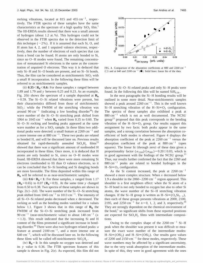
In the next paragraphs the Si–H bonding results willoutlined in some more detail. Near-stoichiometric sampshowed a peak around 2260 cm21. This is the well knownSi–H stretching vibration of the H–Si[O3 configuration.The spectra of these samples also exhibited a peak880 cm21 which is not as well documented. The NCSgroup13 proposed that this peak corresponds to the bendvibration of the H–Si[O3 group. Our results support thiassignment by two facts: both peaks appear in the ssamples, and a strong correlation between the absorptionefficient of both modes is observed. Figure 4 displaysabsorption coefficient of the peak at 2260 cm21 versus theabsorption coefficient of the peak at 880 cm21 ~opensquares!. The linear fit~through zero! of these data gives aproportionality factor (a2260)/(a880)50.2060.03, which isin good agreement with the findings of the NCSU group13
Thus, our results further confirmed the fact that the 2260880 cm21 peaks are related to bonded hydrogen inH–Si[O3 configuration.
As the Si content increased, the peak at 2260 cm21
showed a more complex structure. Whenx decreased below1.9 a shoulder in the 2060– 2200 cm21 region appeared. Thisshoulder is a first neighbors effect: when the Si atom oSi–H bond is not only bonded to oxygen but also to otheratoms, the wave number of the Si–H stretching vibratchanges. If the Si–H group is written as H–Si[(OnSi32n),then each of these groups presents vibrations at 2000, 22195, and 2250 cm21 for n50, 1, 2, and 3, respectively.39
They are strongly dependent on the chemical environmenthe bond,1 so significant shifts from these reported positioare expected for SiOxHy films with intermediate compositions.
Owing to the complex shape of the 2260 cm21 Si–Hpeak when the shoulder was present it was difficult to msure the exact wave number of the intermediate modH–Si[(OSi2) and H–Si[(OSi2). Our results gave valueof 2200 and 2150 cm21 for these modes, respectively. Thewave numbers may be affected by a significant uncertaidue to the very weak absorption of the intermediate modIn spite of this, they were in good agreement with the on
FIG. 4. Comparison of the absorption coefficients at 880 and 2260 cm21
~h! and at 640 and 2100 cm21 ~d!. Solid lines: linear fits of the data.
Reuse of AIP content is subject to the terms at: http://jap.aip.org/about/rights_and_permissions
io
-
sea
ahtoa-nakio
aln
aee
-e
e
a
thto
ofo
inexli-
tivetypes
aec
de-n-
-
ns:
7466 J. Appl. Phys., Vol. 94, No. 12, 15 December 2003 San Andres et al.
calculated by the NCSU group1 for intermediate SiOxHy
compositions.The other peak observed in the high wave number reg
was a mode at 2150– 2050 cm21 ~see Fig. 2!. It correspondsto the H–Si[Si3 stretching vibration in a suboxide environment. This peak became detectable forx values below 1.6.With increasing Si content this peak became more inteneven masking the contributions of other intermediate modFor the samples with this peak a further intense vibration640 cm21 was also detected~see Fig. 2!. This vibration isknown as the bending vibration of the H–Si[Si3 bond.40 InFig. 4 the absorption coefficient of the peak at 2100 cm21 asa function of the absorption coefficient of the peak640 cm21 ~solid circles! is also shown. The linear fit througzero of these data gives a proportionality fac(a2100)/(a640)50.4160.04. Since there is a strong correltion between the absorption coefficient of the 2100 a640 cm21 peaks, these results also confirm that both peare related to bonded hydrogen in the same configurati.e., to the H–Si[Si3 group.
In the case of off-stoichiometric films three additionpeaks of low intensity were detected at 795, 840, a885 cm21 ~see Fig. 2!. Owing to their proximity in wavenumber these peaks were hardly resolved. The peak locat 795 cm21 can be associated to a coupled mode betwSi–H bonds in the same plane as a Si–O–Si bond.41 Thecouple of peaks at 840 and 885 cm21 is a doublet~wagging-bending! for (Si5H2)n groups.14 The presence of this doublet indicates that there is a small amount of hydrogbonded in the form of a dihydride.
Finally, as presented before, the SiH0.36 film did notshow any Si–O related peaks, and only Si–H modes wdetected@Fig. 2~e!#: the expected H–Si[Si3 bending vibra-tion at 640 cm21, the H–Si[Si3 stretching vibration at2060 cm21, and two faint peaks at 840 and 885 cm21 whichare related to silicon dihydride. In this sample the peak795 cm21 did not appear.
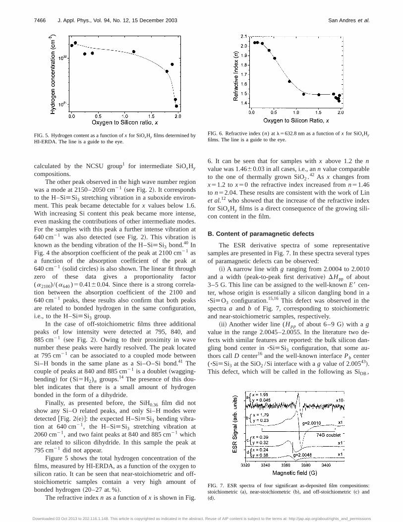
Figure 5 shows the total hydrogen concentration offilms, measured by HI-ERDA, as a function of the oxygensilicon ratio. It can be seen that near-stoichiometric andstoichiometric samples contain a very high amountbonded hydrogen~20–27 at. %!.
The refractive indexn as a function ofx is shown in Fig.
FIG. 5. Hydrogen content as a function ofx for SiOxHy films determined byHI-ERDA. The line is a guide to the eye.
Downloaded 03 Oct 2013 to 202.116.1.148. This article is copyrighted as indicated in the abstract.
n
e,s.t
t
r
dsn,
d
tedn
n
re
t
e
f-f
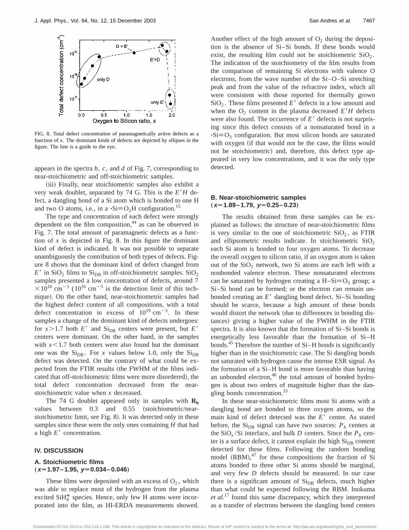
6. It can be seen that for samples withx above 1.2 thenvalue was 1.4660.03 in all cases, i.e., ann value comparableto the one of thermally grown SiO2 .42 As x changes fromx51.2 to x50 the refractive index increased fromn51.46to n52.04. These results are consistent with the work of Let al.12 who showed that the increase of the refractive indfor SiOxHy films is a direct consequence of the growing sicon content in the film.
B. Content of paramagnetic defects
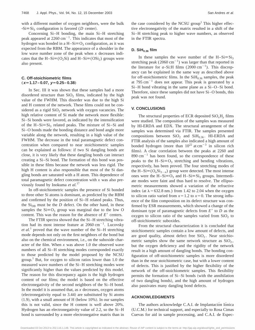
The ESR derivative spectra of some representasamples are presented in Fig. 7. In these spectra severalof paramagnetic defects can be observed:
~i! A narrow line withg ranging from 2.0004 to 2.0010and a width~peak-to-peak first derivative! DHpp of about3–5 G. This line can be assigned to the well-knownE8 cen-ter, whose origin is essentially a silicon dangling bond in"Si[O3 configuration.15,16 This defect was observed in thspectraa and b of Fig. 7, corresponding to stoichiometriand near-stoichiometric samples, respectively.
~ii ! Another wider line (Hpp of about 6–9 G! with a gvalue in the range 2.0045–2.0055. In the literature twofects with similar features are reported: the bulk silicon dagling bond center in"Si[Si3 configuration, that some authors callD center16 and the well-known interfacePb center("Si[Si3 at the SiO2 /Si interface with ag value of 2.00543!.This defect, which will be called in the following as SiDB ,
FIG. 6. Refractive index (n) at l5632.8 nm as a function ofx for SiOxHy
films. The line is a guide to the eye.
FIG. 7. ESR spectra of four significant as-deposited film compositiostoichiometric~a!, near-stoichiometric~b!, and off-stoichiometric~c! and~d!.
Reuse of AIP content is subject to the terms at: http://jap.aip.org/about/rights_and_permissions
a
H
gnn
ntatigom
d-hata
oe
plan
e
a
e
mr
ed
uld
mO
ingallwn
in aedld-pe
ex-s
aseenatrons
un-gonds-
isH
tlyndsl. Asing-an-
athe
ngi
inal,se
atedters
asth
7467J. Appl. Phys., Vol. 94, No. 12, 15 December 2003 San Andres et al.
appears in the spectrab, c, andd of Fig. 7, corresponding tonear-stoichiometric and off-stoichiometric samples.
~iii ! Finally, near stoichiometric samples also exhibitvery weak doublet, separated by 74 G. This is theE8H de-fect, a dangling bond of a Si atom which is bonded to oneand two O atoms, i.e., in a"Si[O2H configuration.15
The type and concentration of each defect were strondependent on the film composition,44 as can be observed iFig. 7. The total amount of paramagnetic defects as a fution of x is depicted in Fig. 8. In this figure the dominakind of defect is indicated. It was not possible to separunambiguously the contribution of both types of defects. Fure 8 shows that the dominant kind of defect changed frE8 in SiO2 films to SiDB in off-stoichiometric samples. SiO2samples presented a low concentration of defects, aroun31016 cm23 (1016 cm23 is the detection limit of this technique!. On the other hand, near-stoichiometric samplesthe highest defect content of all compositions, with a todefect concentration in excess of 1019 cm23. In thesesamples a change of the dominant kind of defects undergfor x.1.7 bothE8 and SiDB centers were present, butE8centers were dominant. On the other hand, in the samwith x,1.7 both centers were also found but the dominone was the SiDB . For x values below 1.0, only the SiDB
defect was detected. On the contrary of what could bepected from the FTIR results~the FWHM of the films indi-cated that off-stoichiometric films were more disordered!, thetotal defect concentration decreased from the nestoichiometric value whenx decreased.
The 74 G doublet appeared only in samples withRbvalues between 0.3 and 0.55~stoichiometric/near-stoichiometric limit, see Fig. 8!. It was detected only in thessamples since these were the only ones containingH that hada highE8 concentration.
IV. DISCUSSION
A. Stoichiometric films„xÄ1.97– 1.95, yÄ0.034– 0.046…
These films were deposited with an excess of O2 , whichwas able to replace most of the hydrogen from the plasexcited SiH4* species. Hence, only few H atoms were incoporated into the film, as HI-ERDA measurements show
FIG. 8. Total defect concentration of paramagnetically active defectsfunction ofx. The dominant kinds of defects are depicted by ellipses infigure. The line is a guide to the eye.
Downloaded 03 Oct 2013 to 202.116.1.148. This article is copyrighted as indicated in the abstract.
ly
c-
e-
7
dl
s:
est
x-
r-
a-.
Another effect of the high amount of O2 during the deposi-tion is the absence of Si–Si bonds. If these bonds woexist, the resulting film could not be stoichiometric SiO2 .The indication of the stoichiometry of the film results frothe comparison of remaining Si electrons with valenceelectrons, from the wave number of the Si–O–Si stretchpeak and from the value of the refractive index, whichwere consistent with those reported for thermally groSiO2 . These films presentedE8 defects in a low amount andwhen the O2 content in the plasma decreasedE8H defectswere also found. The occurrence ofE8 defects is not surpris-ing since this defect consists of a nonsaturated bond"Si[O3 configuration. But most silicon bonds are saturatwith oxygen~if that would not be the case, the films wounot be stoichiometric! and, therefore, this defect type appeared in very low concentrations, and it was the only tydetected.
B. Near-stoichiometric samples„xÄ1.89– 1.79, yÄ0.25– 0.23…
The results obtained from these samples can beplained as follows: the structure of near-stoichiometric filmis very similar to the one of stoichiometric SiO2 , as FTIRand ellipsometric results indicate. In stoichiometric SiO2
each Si atom is bonded to four oxygen atoms. To decrethe overall oxygen to silicon ratio, if an oxygen atom is takout of the SiO2 network, two Si atoms are each left withnonbonded valence electron. These nonsaturated eleccan be saturated by hydrogen creating a H–Si[O3 group; aSi–Si bond can be formed; or the electron can remainbonded creating anE8 dangling bond defect. Si–Si bondinshould be scarce, because a high amount of these bwould distort the network~due to differences in bonding distances! giving a higher value of the FWHM in the FTIRspectra. It is also known that the formation of Si–Si bondsenergetically less favorable than the formation of Si–bonds.45 Therefore the number of Si–H bonds is significanhigher than in the stoichiometric case. The Si dangling bonot saturated with hydrogen cause the intense ESR signathe formation of a Si–H bond is more favorable than havan unbonded electron,46 the total amount of bonded hydrogen is about two orders of magnitude higher than the dgling bonds concentration.33
In these near-stoichiometric films most Si atoms withdangling bond are bonded to three oxygen atoms, somain kind of defect detected was theE8 center. As statedbefore, the SiDB signal can have two sources:Pb centers atthe SiOx /Si interface, and bulkD centers. Since thePb cen-ter is a surface defect, it cannot explain the high SiDB contentdetected for these films. Following the random bondimodel ~RBM!,47 for these compositions the fraction of Satoms bonded to three other Si atoms should be margand very fewD defects should be measured. In our cathere is a significant amount of SiDB defects, much higherthan what could be expected following the RBM. Inokumet al.17 found this same discrepancy, which they interpreas a transfer of electrons between the dangling bond cen
ae
Reuse of AIP content is subject to the terms at: http://jap.aip.org/about/rights_and_permissions
ul
nge
th
o
Soneletiodo
heo
pler
acosThanf
eBue
ra
ingb
havectSeee
geivndss
%i–n
eved
n
bove
y a
, this
urede
nted
t of
ndese,s ofse
so-tiven
on-f the
hatand
iOrkon-edentey
n
asec-
7468 J. Appl. Phys., Vol. 94, No. 12, 15 December 2003 San Andres et al.
with a different number of oxygen neighbors, were the b"Si[Si3 configuration is favored (D center!.
Concerning Si–H bonding, the main Si–H stretchipeak appeared at 2260 cm21. This indicates that most of thhydrogen was bonded in a H–Si[O3 configuration, as it wasexpected from the RBM. The appearance of a shoulder inlow wave number zone of the peak whenx decreases indi-cates that the H–Si[(O2Si) and H–Si[(OSi2) groups werealso present.
C. Off-stoichiometric films„xÄ1.17– 0.07, yÄ0.25– 0.38…
In Sec. III it was shown that these samples had a mdisordered structure than SiO2 films, indicated by the highvalue of the FWHM. This disorder was due to the highand H content of the network. These films could not be csidered as a rigid SiO2 network with oxygen vacancies. Thhigh relative content of Si made the network more flexibSi–Si bonds were favored, as indicated by the intensificaof the H–Si[Si3 related peaks. The mixture of Si–Si anSi–O bonds made the bonding distance and bond angle mvariable along the network, resulting in a high value of tFWHM. The decrease in the total paramagnetic defect ccentration when compared to near stoichiometric samcan be explained as follows: if two Si dangling bonds aclose, it is very likely that these dangling bonds can intercreating a Si–Si bond. The formation of this bond was psible in these films because the network was less rigid.high H content is also responsible that most of the Si dgling bonds are saturated with a H atom. This dependence ototal paramagnetic defect concentration withx was also pre-viously found by Inokumaet al.17
In off-stoichiometric samples the presence of Si bondto three other Si atoms is dominant, as predicted by the Rand confirmed by the position of Si–H related peaks. Ththe SiDB must be theD defect. On the other hand, in thessamples the Si[O3 group was marginal due to the low Ocontent. This was the reason for the absence ofE8 centers.
The FTIR spectra showed that the Si–H stretching vibtion had its most intense feature at 2060 cm21. Lucovskyet al.1 proved that the wave number of the Si–H stretchmode depends not only on the first neighbors of the bondalso on the chemical environment, i.e., on the suboxide cacter of the film. Whenx was above 1.0 the observed wanumbers of all Si–H stretching modes corresponded exato those predicted by the model proposed by the NCgroup.1 But, for oxygen to silicon ratios lower than 1.0 thmeasured wave numbers of the Si–H stretching modes wsignificantly higher than the values predicted by this modThe reason for this discrepancy again is the high hydrocontent of our films; the model is based on the effectelectronegativity of the second neighbors of the Si–H boIn the model it is assumed that, asx decreases, oxygen atom~electronegativity equal to 3.44! are substituted by Si atom~1.9!, with a small amount of H~below 10%!. In our samplesthis is not valid, since the H content is well above 20Hydrogen has an electronegativity value of 2.2, so the Sbond is surrounded by a more electronegative matrix tha
Downloaded 03 Oct 2013 to 202.116.1.148. This article is copyrighted as indicated in the abstract.
k
e
re
i-
:n
re
n-s
et-e-
dMs,
-
utr-
lyU
rel.n
e.
.Hin
the case considered by the NCSU group1 This higher effec-tive electronegativity of the matrix resulted in a shift of thSi–H stretching peak to higher wave numbers, as obserin the FTIR spectra.
D. SiH0.36 film
In these samples the wave number of the H–Si[Si3stretching peak (2060 cm21) was larger than that reported ithe literature fora-Si:H films (2000 cm21). This discrep-ancy can be explained in the same way as described afor off-stoichiometric films. In the SiH0.36 samples, the peakat 795 cm21 does not appear. This peak is generated bSi–H bond vibrating in the same plane as a Si–O–Sibond.Therefore, since these samples did not have Si–O bondspeak was not found.
V. CONCLUSIONS
The structural properties of ECR deposited SiOxHy filmswere studied. The composition of the samples was measby HI-ERDA and EDX. The structural arrangement of thsamples was determined via FTIR. The samples presecompositions between SiO2 and SiH0.36. HI-ERDA andFTIR analysis of the samples also indicated a high amounbonded hydrogen~more than 1022 at cm23 in silicon richfilms!. A clear correlation between the peaks at 2260 a890 cm21 has been found, so the correspondence of thpeaks to the H–Si[O3 stretching and bending vibrationsrespectively, has been proved. The four stretching modethe H–Si[(OnSi32n) group were detected. The most intenones were the H–Si[O3 and H–Si[Si3 groups. Intermedi-ate modes were faint and thus hard to resolve. The ellipmetric measurements showed a variation of the refracindex ~at l5632.8 nm.) from 1.42 to 2.04 when the oxygeto silicon ratio varied fromx51.2 tox50. The strong influ-ence of the film composition on its defect structure was cfirmed by ESR measurements, which showed a change odominant type of paramagnetic defects fromE8 to D as theoxygen to silicon ratio of the samples varied from SiO2 tooff-stoichiometric suboxides.
From the structural characterization it is concluded tstoichiometric samples contain a low amount of defects,are good quality, almost defect free SiO2 . Near stoichio-metric samples show the same network structure as S2 ,but the oxygen deficiency and the rigidity of the networesult in a high amount of dangling bonds. The bonding cfiguration of off-stoichiometric samples is more disorderthan in the near stoichiometric case, but with a lower contof defects. This is justified by the higher flexibility of thnetwork of the off-stoichiometric samples. This flexibilitpermits the formation of Si–Si bonds~with the annihilationof two dangling bonds!, and the high amount of hydrogealso passivates many dangling bond defects.
ACKNOWLEDGMENTS
The authors acknowledge C.A.I. de Implantacio´n Ionica~U.C.M.! for technical support, and especially to Rosa CimCuevas for aid in sample processing, and C.A.I. de Esp
Reuse of AIP content is subject to the terms at: http://jap.aip.org/about/rights_and_permissions
c-is
ch
ke
B.
p
ex
,ci
pp
. B
on
p
C
, J
ett
ppl.
.
s.
n
c.
.
tro-
nd
ev.
7469J. Appl. Phys., Vol. 94, No. 12, 15 December 2003 San Andres et al.
troscopia~U.C.M.! for providing access to the FTIR spetrometer. This work was partially supported by the SpanCICYT, under Contract No. TIC 01-1253.
1G. Lucovsky, J. Non-Cryst. Solids227-230, 1 ~1998!.2K. T. Queeney, M. K. Weldon, J. P. Chang, Y. J. Chabal, A. B. GureviJ. Sapjeta, and R. L. Opila, J. Appl. Phys.87, 1322~2000!.
3G. B. Alers, D. J. Werder, Y. Chabal, H. C. Lu, E. P. Gusev, E. GarfunT. Gustafsson, and R. S. Urdahl, Appl. Phys. Lett.73, 1517~1998!.
4F. Irrera and F. Russo, IEEE Trans. Electron DevicesED-46, 2315~1999!.5I. Crupi, S. Lombardo, C. Spinella, C. Bongiormo, Y. Liao, C. Gerardi,Fazio, M. Vulpio, and S. Privitera, J. Appl. Phys.89, 5552~2001!.
6D. N. Kouvatsos, V. Ioannou-Sougleridis, and A. G. Nassiopoulou, ApPhys. Lett.82, 397 ~2003!.
7U. Kahler and H. Hofmeister, Appl. Phys. A: Mater. Sci. Process.74, 13~2002!.
8D. Nesheva, C. Raptis, A. Perakis, I. Bineva, Z. Aneva, Z. Levi, S. Alandrova, and H. Hofmeister, J. Appl. Phys.82, 4678~2002!.
9G. Franzo`, A. Irrera, E. C. Moreira, M. Miritello, F. Iacoma, D. SanfilippoG. Di Stefano, P. G. Fallica, and F. Priolo, Appl. Phys. A: Mater. SProcess.74, 1 ~2002!.
10M. L. Green, E. P. Gusev, R. Degraeve, and E. L. Garfunkel, J. APhys.90, 2057~2001!.
11S. M. Sze,Physics of Semiconductor Devices, ~Wiley, New York, 1981!.12C. Lin, W. Tseng, M. S. Feng, and B. Lee, J. Appl. Phys.87, 2808~2000!.13D. V. Tsu, G. Lucovsky, and B. N. Davidson, Phys. Rev. B40, 1795
~1989!.14M. Zacharias, D. Dimova-Malinovska, and M. Stutzmann, Philos. Mag
73, 799 ~1996!.15P. M. Lenahan and J. F. Conley, Jr., J. Vac. Sci. Technol. B16, 2134
~1998!.16T. Inokuma, L. He, Y. Kurata, and S. Hasegawa, J. Electrochem. Soc.142,
2346 ~1995!.17E. Holzenkampfer, F.-W. Richter, J. Stuke, and U. Voget-Grote, J. N
Cryst. Solids32, 327 ~1979!.18P. V. Bulkin, P. L. Swart, and B. M. Lacquet, J. Non-Cryst. Solids226, 58
~1998!.19K. Yoshida, I. Umezu, N. Sakamoto, M. Inada, and A. Sugimura, J. Ap
Phys.92, 5936~2002!.20D. Nesheva, I. Bineva, Z. Levi, Z. Aneva, T. Merdzhanova, and J.
Pivin, Vacuum68, 1 ~2003!.21K. Miyake, S. Kimura, T. Warabisako, H. Sunami, and T. Tokuyama
Vac. Sci. Technol. A2, 496 ~1984!.22B. H. Lee, Y. Jeon, K. Zawadzki, W.-J. Qi, and J. Lee, Appl. Phys. L
74, 3143~1999!.23T. P. Ma, IEEE Trans. Electron DevicesED-45, 680 ~1998!.
Downloaded 03 Oct 2013 to 202.116.1.148. This article is copyrighted as indicated in the abstract.
h
,
l,
l.
-
.
l.
-
l.
.
.
.
24M. Losurdo, P. Capezzuto, G. Bruno, G. Perna, and V. Capozzi, APhys. Lett.81, 16 ~2002!.
25P. K. Shufflebotham, D. J. Thomson, and H. C. Card, J. Appl. Phys.64,4398 ~1988!.
26F. L. Martınez, E. San Andre´s, A. del Prado, I. Ma´rtil, D. Bravo, and F. J.Lopez, J. Appl. Phys.90, 1573~2001!.
27F. L. Martinez, A. Del Prado, I. Ma´rtil, G. Gonzalez-Dıaz, W. Bohne, W.Fuhs, J. Ro¨rich, B. Selle, and I. Sieber, Phys. Rev. B63, 245320~2001!.
28W. Bohne, J. Ro¨hrich, and G. Ro¨schert, Nucl. Instrum. Methods PhysRes. B136-138, 633 ~1998!.
29W. Bohne, S. Hessler, and G. Ro¨schert, Nucl. Instrum. Methods Phys. ReB 113, 78 ~1996!.
30W. Bohne, W. Fuhs, J. Ro¨hrich, B. Selle, I. Sieber, A. del Prado, E. SaAndres, I. Martil, and G. Gonza´lez-Dıaz, Surf. Interface Anal.34, 749~2002!.
31G. F. Bastin and H. J. M. Heijligers, Scanning12, 225 ~1990!.32B. J. Hinds, F. Wang, D. M. Wolfe, C. L. Hinkle, and G. Lucovsky, J. Va
Sci. Technol. B16, 2171~1998!.33E. San Andre´s, A. del Prado, I. Ma´rtil, G. Gonzalez-Dıaz, D. Bravo, and F.
J. Lopez, J. Appl. Phys.92, 1906~2002!.34F. Rochet, G. Dufour, H. Roulet, B. Pelloie, J. Perrie`re, E. Fogarassy, A.
Slaoui, and M. Froment, Phys. Rev. B37, 6468~1988!.35A. Sasella, A. Borghesi, F. Corni, A. Monelli, G. Ottaviani, R. Tonini, B
Pivac, M. Bachetta, and L. Zanotti, J. Vac. Sci. Technol. A15, 377~1997!.36D. Landheer, Y. Tao, J. E. Hulse, T. Quance, and D.-X. Xu, J. Elec
chem. Soc.143, 1681~1996!.37E. San Andre´s, A. del Prado, F. L. Martı´nez, I. Martil, D. Bravo, and F. J.
Lopez, J. Appl. Phys.87, 1187~2000!.38K. Furukawa, Y. Liu, H. Nakashima, D. Gao, K. Uchino, K. Muraoka, a
H. Tsuzuki, Appl. Phys. Lett.72, 725 ~1998!.39L. He, Y. Kurata, T. Inokuma, and S. Hasegawa, Appl. Phys. Lett.63, 162
~1993!.40G. Lucovsky, J. Yang, S. S. Chao, J. E. Tyler, and W. Czubatyj, Phys. R
B 28, 3225~1983!.41G. Lucovsky and W. B. Pollard, J. Vac. Sci. Technol. A1, 313 ~1983!.42Handbook of Optical Constants of Solids, edited by E. D. Palik~Aca-
demic, Orlando, FL, 1985!.43M. J. Uren, J. H. Stathis, and E. Cartier, J. Appl. Phys.80, 3915~1996!.44E. San Andre´s, A. del Prado, I. Ma´rtil, G. Gonzalez-Dıaz, F. L. Martı´nez,
D. Bravo, and F. J. Lo´pez, Vacuum67, 531 ~2002!.45L. He, T. Inokuma, and S. Hasegawa, Jpn. J. Appl. Phys., Part 135, 1503
~1996!.46H. Angermann, W. Henrion, and A. Ro¨seler,Silicon-Based Materials and
Devices, Vol. 1: Materials and Processing~Academic, New York, 2001!Chap. 7, p. 267.
47H. R. Philipp, J. Phys. Chem. Solids32, 1935~1971!.
Reuse of AIP content is subject to the terms at: http://jap.aip.org/about/rights_and_permissions
Related Documents