○Product structure:Silicon monolithic integrated circuit ○This product has no designed protection against radioactive rays . 1/17 TSZ02201-0J2J0A601070-1-2 © 2015 ROHM Co., Ltd. All rights reserved. 02.Nov.2015 Rev.001 TSZ22111・14・001 www.rohm.com 0.65V to 5.5V, 1ch Ultra Low Dropout Linear Regulator Controller BD3504FVM General Description BD3504FVM is an ultra-low dropout linear regulator controller for chipset that can achieve ultra-low input to output voltage. By using N-MOSFET for external power transistor, the controller can be used at ultra-low I/O voltage difference as low as the voltage generated by ON-Resistance. By reducing the I/O voltage difference, large output current is achieved and conversion loss can be reduced, thus the controller can be used in replacement of a switching power supply. In addition, downsizing and cost reduction of the set can be achieved as suitable power transistor can be selected depending on the output current. BD3504FVM does not need any choke coil, diode for rectification and power transistor which are all necessary in a switching power supply, thus reduced total cost and compact size can be achieved for the set. Using external resistors, output voltage ranging from 0.65V to 2.5V can be selected. It is also possible to meet the power supply sequence of the set since output voltage start-up time can be adjusted by using the NRCS terminal. Features Reduced rush current by NRCS Built-in driver for external Nch transistor Built-in timer latch short protection circuit Built-in under voltage lock out circuit Output voltage variable type Built-in thermal shutdown circuit Key Specifications Drain Voltage Range: 0.65V to 5.5V Supply Voltage Range: 4.5V to 5.5V Output Voltage Range: 0.65V to 2.5V External FET GATE Drive Current: ±3mA(Typ) Standby Current: 0μA (Typ) Operating Temperature Range: -10°C to +100°C Package W(Typ) x D(Typ) x H(Max) Applications Mobile PC, desktop PC, digital home appliances Typical Application Circuit and Block Diagram 8 Reference Block Thermal Protection VCC VCC UVLO1 VD UVLO LATCH UVLO2 UVLO1 EN TSD SCP UVLO1 UVLO2 EN NRCS 0.65V VFB G VD VS EN Enable 0.65V NRCS SCP SCP GND NRCS NRCS 0.65V TSD VREF 4 3 1 2 5 6 7 8 MSOP8 2.90mm x 4.00mm x 0.90mm R2’ R1’ R2 R1 IN OUT Datasheet Datasheet

Welcome message from author
This document is posted to help you gain knowledge. Please leave a comment to let me know what you think about it! Share it to your friends and learn new things together.
Transcript

○Product structure:Silicon monolithic integrated circuit ○This product has no designed protection against radioactive rays
.
1/17 TSZ02201-0J2J0A601070-1-2
© 2015 ROHM Co., Ltd. All rights reserved. 02.Nov.2015 Rev.001 TSZ22111・14・001
www.rohm.com
0.65V to 5.5V, 1ch Ultra Low Dropout Linear Regulator Controller BD3504FVM General Description
BD3504FVM is an ultra-low dropout linear regulator controller for chipset that can achieve ultra-low input to output voltage. By using N-MOSFET for external power transistor, the controller can be used at ultra-low I/O voltage difference as low as the voltage generated by ON-Resistance. By reducing the I/O voltage difference, large output current is achieved and conversion loss can be reduced, thus the controller can be used in replacement of a switching power supply. In addition, downsizing and cost reduction of the set can be achieved as suitable power transistor can be selected depending on the output current. BD3504FVM does not need any choke coil, diode for rectification and power transistor which are all necessary in a switching power supply, thus reduced total cost and compact size can be achieved for the set. Using external resistors, output voltage ranging from 0.65V to 2.5V can be selected. It is also possible to meet the power supply sequence of the set since output voltage start-up time can be adjusted by using the NRCS terminal.
Features Reduced rush current by NRCS Built-in driver for external Nch transistor Built-in timer latch short protection circuit Built-in under voltage lock out circuit Output voltage variable type Built-in thermal shutdown circuit
Key Specifications
Drain Voltage Range: 0.65V to 5.5V Supply Voltage Range: 4.5V to 5.5V Output Voltage Range: 0.65V to 2.5V External FET GATE Drive Current: ±3mA(Typ) Standby Current: 0µA (Typ) Operating Temperature Range: -10°C to +100°C
Package W(Typ) x D(Typ) x H(Max)
Applications Mobile PC, desktop PC, digital home appliances
Typical Application Circuit and Block Diagram
8
Reference
Block
Thermal
Protection
VCC
VCC
UVLO1
VD
UVLO
LATCH
UVLO2
UVLO1
EN
TSD
SCP
UVLO1
UVLO2
EN
NRCS
0.65V
VFB
G
VD
VS
R2
R1
VIN
Vo
EN Enable
0.65V
NRCS
SCP
SCP
GND NRCS
NRCS
0.65V
R1’
R2’
TSD
VREF
4
3
1 2
5
6
7
8
MSOP8 2.90mm x 4.00mm x 0.90mm
R2’
R1’
R2
R1
IN
OUT
Datasheet
Datasheet

BD3504FVM
2/17
© 2015 ROHM Co., Ltd. All rights reserved. www.rohm.com
TSZ22111・15・001
TSZ02201-0J2J0A601070-1-2
02.Nov.2015 Rev.001
Pin Configuration
Pin Descriptions
PinNo.
Pin Name Pin Function
1 NRCS
NRCS (Non Rush Current on Start up) time setup. Timer latch setup for Short Circuit Protection operating time set up Pin.
2 GND Ground pin
3 EN Enable pin
4 VCC Power source
5 VFB Output voltage feedback
6 VS Source voltage pin
7 G MOSFET driver output
8 VD Drain voltage sense
Description of Operations
1. VCC BD3504FVM has an independent power input pin for the internal circuit operation of the IC. This is used to bias the IC internal circuit and external N-Channel MOSFET. The voltage used for VCC terminal is 5.0V and maximum current is 1.7mA. It is recommended to connect a bypass capacitor with a value of 1µF or more to VCC pin.
2. EN
With an input of 2.0V or higher, the EN terminal turns to “High” level and OUT is produced. At 0.8V or lower, it detects “Low” level and OUT is turned OFF. Simultaneously, the discharge circuit inside the VS terminal is activated and output voltage is reduced (150 mA (Min) when VVS=1V and VEN=0V).
3. VD
The VD terminal is the drain voltage detection terminal of the external N-Channel MOSFET. When drain voltage (IN) is low, output voltage is turned OFF to prevent under voltage lock out. The reset voltage (VDUVLO) of under voltage lock out circuit is determined by the following equation:
'
''7.0
1
21
R
RRVV INVDUVLO
At low-input drain voltage, when UVLO resistors have resistance values same as output voltage resistors (R1 = R1’, R2 = R2’), under voltage lock out (UVLO) is reset when drain voltage (IN) reaches 70% of the output voltage. UVLO detects only at the startup of the EN terminal.
4. VFB
The VFB terminal is use to decide the output voltage and is determined by the following equation:
1
21
R
RRVV VFBOUT
where: VVFB is controlled to achieve 0.65 V (typ).
5. NRCS terminal
The NRCS terminal is a constant current output terminal, and operates as Soft-Start ... during start-up SCP-Delay ... after start-up
How to set Soft-Start of NRCS terminal The output voltage startup time (tNRCS) is determined by the time when the NRCS terminal reaches VVFB (0.65V). During start-up, the NRCS terminal serves as a constant current source (INRCS) of 20 µA (Typ) output, and charges externally connected capacitor (CNRCS). Output voltage (VOUT) becomes stable when NRCS terminal reaches the internal reference voltage (0.65V).
How to set NRCS terminal short protection Delay BD3504FVM has short circuit protection (SCP) which is activated when output voltage becomes VOUT x 0.35 (typ) or lower. The time when SCP is activated until latch takes place (tSCP) is determined by the following equation:
SCPOSCPNRCSSCP IVCt
When SCP is activated, the NRCS terminal provides 20 µA (typ) constant current output (lSCP), and charges the externally connected capacitor (CNRCS). When the NRCS terminal reaches 1.3V (VOSCP), latch operation is carried out and output voltage is turned OFF.
1
2
3
4 5
6
7
8
G
VD
VS
VFB
NRCS
GND
EN
VCC
TOP VIEW

BD3504FVM
3/17
© 2015 ROHM Co., Ltd. All rights reserved. www.rohm.com
TSZ22111・15・001
TSZ02201-0J2J0A601070-1-2
02.Nov.2015 Rev.001
Description of Operations – continued
6. VS
VS terminal is a source voltage detection terminal of the external N-Channel MOSFET. VFB//VS terminal has the internal discharge circuit activated to lower output voltage when EN changes to Low level or various protection circuits (TSD, SCP, UVLO) are activated.
7. G
G terminal is the gate drive terminal of the external N-Channel MOSFET. Because the output voltage range of G terminal is up to 5V (VCC), it is necessary to use N-Channel MOSFET whose threshold is lower than “5V - VOUT”. In addition, by including an RC snubber circuit to the G terminal, phase margin of loop gain can be increased and ceramic capacitors can be used for the terminal.
Absolute Maximum Ratings (Ta=25°C)
Parameter Symbol Rating Unit
Supply Voltage VCC 7 (Note 1) V
Drain Voltage VVD 7 V
Enable Input Voltage VEN 7 V
Power Dissipation Pd 0.43 (Note 2) W
Operating Temperature Range Topr -10 to +100 °C
Storage Temperature Range Tstg -55 to +150 °C
Maximum Junction Temperature Tjmax +150 °C
(Note 1) However, not exceeding Pd. (Note 2) To use at temperature above Ta=25°C, derate by 3.5mW/°C Caution: Operating the IC over the absolute maximum ratings may damage the IC. The damage can either be a short circuit between pins or an open
circuit between pins and the internal circuitry. Therefore, it is important to consider circuit protection measures, such as adding a fuse, in case the IC is operated over the absolute maximum ratings.
Recommended Operating Conditions
Parameter Symbol Rating
Unit Min Max
Supply Voltage VCC 4.5 5.5 V
Drain Voltage VVD 0.65 5.5 V
Enable Input Voltage VEN -0.3 +5.5 V
Capacitor in NRCS Pin CNRCS 0.001 1 µF
Output Voltage VOUT 0.65 2.5 V
Electrical Characteristics (Unless otherwise specified, Ta=25°C VCC=5V VIN=3.3V VEN=3V R1=R1'=∞Ω, R2=R2'=0Ω)
Parameter Symbol Standard Value
Unit Conditions Min Typ Max
Circuit Current ICC - 0.85 1.7 mA
Shut Down Mode Current IST - 0 10 µA VEN=0V
Feed Back Voltage 1 VVFB1 0.643 0.650 0.657 V IOUT=50mA
Feed Back Voltage 2 VVFB2 0.630 0.650 0.670 V VCC=4.5V to 5.5V , Ta=-10°C to +100°C (Note)
Output Voltage VOUT - 1.20 - V R1=R1'=3.9kΩ, R2=R2'=3.3KΩ
Line Regulation Reg.l - 0.1 0.5 %/V VCC=4.5V to 5.5V
Load Regulation Reg.L - 0.5 10 mV IOUT=0A to 3A
[Enable]
High Level Enable Input Voltage VENHI 2 - VCC V
Low Level Enable Input Voltage VENLOW -0.3 - +0.8 V
Enable Pin Input Current IEN - 7 10 µA VEN=3V
(Note) Not 100% tested

BD3504FVM
4/17
© 2015 ROHM Co., Ltd. All rights reserved. www.rohm.com
TSZ22111・15・001
TSZ02201-0J2J0A601070-1-2
02.Nov.2015 Rev.001
Electrical Characteristics- continued (Unless otherwise specified, Ta=25°C VCC=5V VIN=3.3V VEN=3V R1=R1'=∞Ω, R2=R2'=0Ω)
Parameter Symbol Standard Value
Unit Conditions Min Typ Max
[Voltage Feed Back]
VFB Input Bias Current IVFB - 80 - nA
[Source Voltage]
VS Input Bias Current ISBIAS - 1.2 2.4 mA
VS Standby Current ISSTB 150 - - mA VVS=1V VEN=0V
[Output MOSFET Driver]
MOSFET Driver Source Current IGSO 2 3 4 mA VVFB=0.6V, VGATE=2.5V
MOSFET Driver Sink Current IGSI 2 3 4 mA VVFB=0.7V, VGATE=2.5V
[UVLO]
VCC UVLO VCCUVLO 4.20 4.35 4.50 V VCC: Sweep up
VCC UVLO Hysterisis VCCHYS 100 160 220 mV VCC: Sweep down
VD UVLO VVDUVLO VOUTx0.6 VOUTx0.7 VOUTx0.8 V VD: Sweep up
[Drain Voltage Sensing]
VD Input Bias Current IVD - 0 - nA
[NRCS/SCP]
NRCS Charge Current INRCS 14 20 26 µA VNRCS=0.5V
SCP Charge Current ISCPCH 14 20 26 µA VNRCS=0.5V
SCP Discharge Current ISCPDI 0.3 - - mA VNRCS=0.5V
SCP Threshold Voltage VSCP 1.2 1.3 1.4 V
Short Detect Voltage VOSCP VOUTx0.3 VOUTx0.35 VOUTx0.4 V
NRCS Stand-by Voltage VSTB - - 50 mV

BD3504FVM
5/17
© 2015 ROHM Co., Ltd. All rights reserved. www.rohm.com
TSZ22111・15・001
TSZ02201-0J2J0A601070-1-2
02.Nov.2015 Rev.001
Figure 4. Enable Pin Input Current vs Temperature
6
7
8
9
10
11
12
25 50 75 100 125 150
Temperature : Ta (°C)
En
ab
le P
in In
put
Curr
ent
: I E
N (
µA
)
Typical Performance Curves
Figure 2. Circuit Current vs Supply Voltage Figure 1. Standby Current vs Temperature
0.00
0.20
0.40
0.60
0.80
1.00
1.20
1.40
-60 -10 40 90 140
Ta(℃) Temperature : Ta (°C)
Sta
nd
by C
urr
en
t :
I ST
B (µ
A)
0.00
0.20
0.40
0.60
0.80
4.5 4.7 4.9 5.1 5.3 5.5
VCC(V) Supply Voltage : VCC (V)
Cir
cu
it C
urr
ent
: I C
C (m
A)
Figure 3. Output Voltage vs Temperature
1.770
1.775
1.780
1.785
1.790
1.795
1.800
-10 15 40 65 90
Temperature : Ta (°C)
Ou
tpu
t V
oltag
e :
VO
UT (
V)

BD3504FVM
6/17
© 2015 ROHM Co., Ltd. All rights reserved. www.rohm.com
TSZ22111・15・001
TSZ02201-0J2J0A601070-1-2
02.Nov.2015 Rev.001
Typical Performance Curves – continued
18.5
19
19.5
20
20.5
21
21.5
-60 40 140
Ta(℃)
IS
CP
(uA
)Figure 6. ISCP vs Temperature
I SC
P (µ
A)
Temperature : Ta (°C)
Figure 5. VS Discharge Current vs Output Voltage
Figure 7. VBG vs Temperature
1.23
1.235
1.24
1.245
1.25
1.255
1.26
-60 -10 40 90 140
Ta(℃)
VB
G(V
)
Temperature : Ta (°C)
VB
G (V
)
I S (m
A)
Output Voltage : VOUT (mV)
0
50
100
150
200
250
300
0 0.2 0.4 0.6 0.8 1 1.2
BD3504FVM
7/17
© 2015 ROHM Co., Ltd. All rights reserved. www.rohm.com
TSZ22111・15・001
TSZ02201-0J2J0A601070-1-2
02.Nov.2015 Rev.001
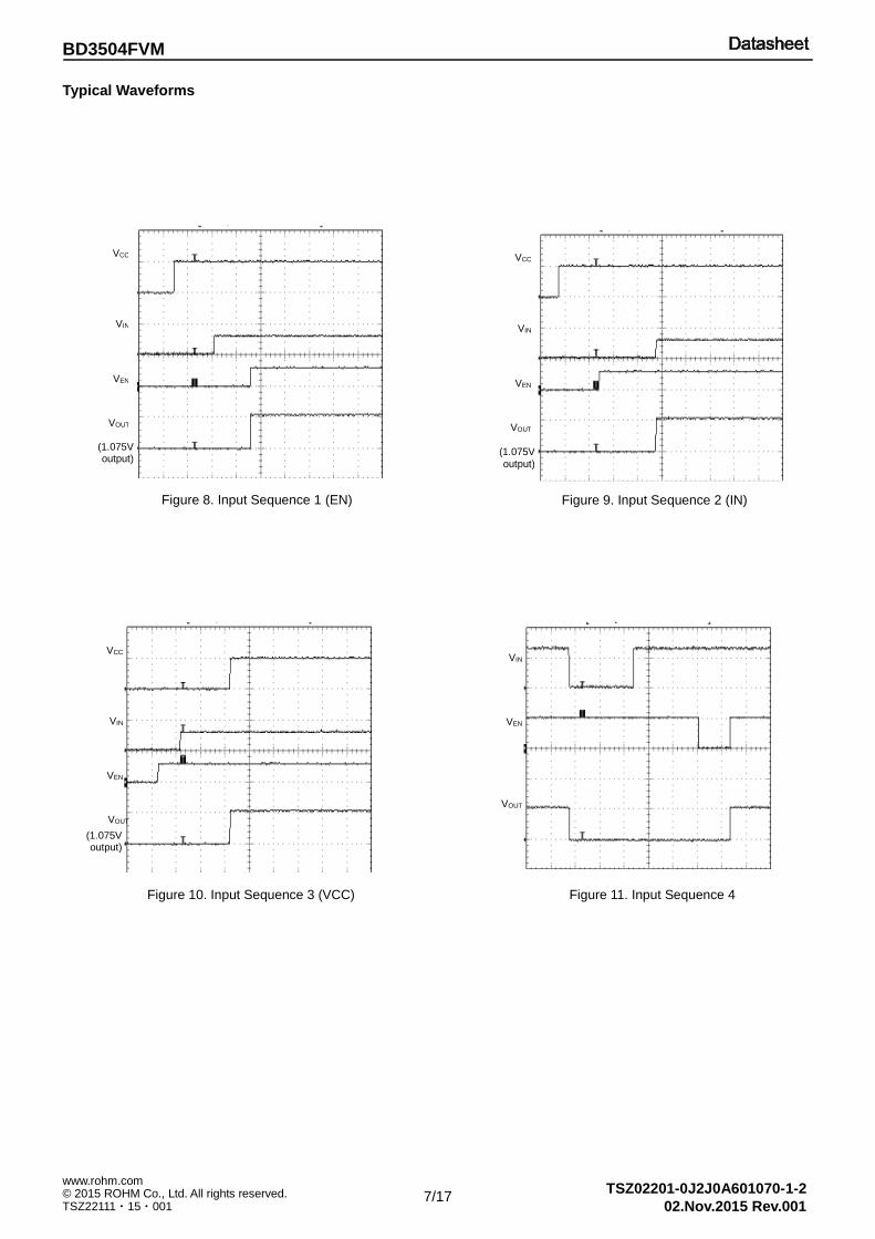
Typical Waveforms
Figure 8. Input Sequence 1 (EN) Figure 9. Input Sequence 2 (IN)
Figure 10. Input Sequence 3 (VCC)
VCC
VIN
VEN
VOUT
(1.075V output)
VCC
VIN
VEN
VOUT
(1.075V
output)
VCC
VIN
VEN
VOUT
(1.075V output)
Figure 11. Input Sequence 4
VIN
VEN
VOUT
BD3504FVM
8/17
© 2015 ROHM Co., Ltd. All rights reserved. www.rohm.com
TSZ22111・15・001
TSZ02201-0J2J0A601070-1-2
02.Nov.2015 Rev.001
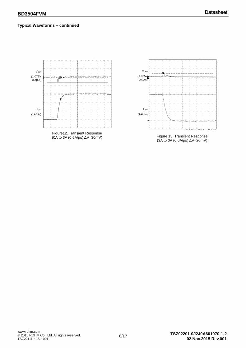
Typical Waveforms – continued
Figure12. Transient Response (0A to 3A (0.6A/µs) ΔV=30mV) Figure 13. Transient Response
(3A to 0A (0.6A/µs) ΔV=20mV)
VOUT
IOUT
(1.075V output)
(1A/div)
VOUT
IOUT
(1.075V output)
(1A/div)

BD3504FVM
9/17
© 2015 ROHM Co., Ltd. All rights reserved. www.rohm.com
TSZ22111・15・001
TSZ02201-0J2J0A601070-1-2
02.Nov.2015 Rev.001
Application Information
1. Application Circuit
VIN
R1’
R2’
C3
Ven C4
C1 Vcc
+
1
2
3
4
8
7
6
5
C2
R1
R2
2. Directions for Pattern Layout of PCB
(1) Because IN input capacitor causes impedance to drop, mount it as close as possible to the IN terminal using thick wiring patterns. When it causes the wire to come in contact with the inner-layer ground plane, multiple through holes connection.
(2) Because NRCS terminal is analog I/O, be careful of noise. In particular, high-frequency noise of GND may cause IC
malfunction through capacitors. It is recommended to connect the GND terminal of NRCS capacitor to the IC GND terminal at a single point.
(3) The VFB terminal is an output voltage sense line. Effects of wiring impedance can be ignored by sensing the output
voltage from the load side, but increased sense wiring causes VFB to be susceptible to noise, in which care must be taken.
(4) Because the GND terminal is the same GND to be used inside the analog circuit of BD3504FVM, connect it to the
inner-layer GND of substrate at a single point using a pattern that is as short as possible. Place a bypass capacitor across VCC and GND as close as possible so that a loop can be minimized.
(5) The G terminal is the terminal for gate drive. If long wiring will be used, increase the pattern width to lower impedance.
(6) Heat generated in the output transistor can be calculated by:
MaxIVV OUTOUTIN
Design heat generation not to exceed the guaranteed temperature of transistors.
(7) Connect the output capacitor using thick short wirings so that the impedance is minimized. Connect capacitor GND terminal to the inner-layer GND plane by multiple through holes connection.
VEN
C3 C2
R1’
R2’
R2
R1’
R1
R1’
C4
R1’
C1
R1’ VCC
R1’
R1’
R1’
VIN
R1’

BD3504FVM
10/17
© 2015 ROHM Co., Ltd. All rights reserved. www.rohm.com
TSZ22111・15・001
TSZ02201-0J2J0A601070-1-2
02.Nov.2015 Rev.001
Silk Screen TOP Layer Bottom Layer
3. Evaluation Board
■BD3504FVM Evaluation Board Circuit ■BD3504FVM Evaluation Board Application Components
■ BD3504FVM Evaluation Board Layout
Part No Value Company Parts Name
U1 - ROHM BD3504FVM
U2 NMOS ROHM RTW060N03
R1 3.9K ROHM MCR03EZPF3901
R1’ 3.3K ROHM MCR03EZPF3301
R2 3.9K ROHM MCR03EZPF3901
Part No Value Company Parts Name
R2’ 3.3K ROHM MCR03EZPF3301
C1 1µF MURATA GRM18 series
C2 0.01µF MURATA GRM18 series
C3 10µF MURATA GRM21 series
C4 220µF SANYO,etc 2R5TPE220MF
BD3504FVM
G
EN
VCC
NRCS
VD
VS
GND
VCC
S1 3
6
5
7
U1
VFB
GND
VTTS
1
C1
4
2
VCC
8 VIN
VOUT C2
C3
C4
U2
R2’
R1’
R2
R1 R1
R2 C4
C3
VOUT
R1’
VCC
S1
C2
C1
R2’
VIN
BD3504FVM
11/17
© 2015 ROHM Co., Ltd. All rights reserved. www.rohm.com
TSZ22111・15・001
TSZ02201-0J2J0A601070-1-2
02.Nov.2015 Rev.001
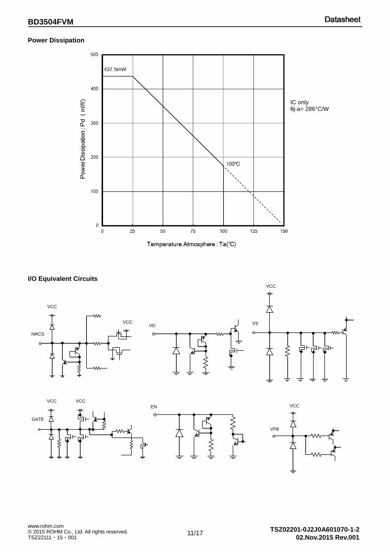
Power Dissipation
I/O Equivalent Circuits
IC only
θj-a= 286°C/W
NRCS
VCC
VCC VD
EN
GATE
VCC VCC
VFB
VCC
VS
VCC

BD3504FVM
12/17
© 2015 ROHM Co., Ltd. All rights reserved. www.rohm.com
TSZ22111・15・001
TSZ02201-0J2J0A601070-1-2
02.Nov.2015 Rev.001
Operational Notes
1. Reverse Connection of Power Supply
Connecting the power supply in reverse polarity can damage the IC. Take precautions against reverse polarity when connecting the power supply, such as mounting an external diode between the power supply and the IC’s power supply pins.
2. Power Supply Lines
Design the PCB layout pattern to provide low impedance supply lines. Separate the ground and supply lines of the digital and analog blocks to prevent noise in the ground and supply lines of the digital block from affecting the analog block. Furthermore, connect a capacitor to ground at all power supply pins. Consider the effect of temperature and aging on the capacitance value when using electrolytic capacitors.
3. Ground Voltage
Ensure that no pins are at a voltage below that of the ground pin at any time, even during transient condition.
4. Ground Wiring Pattern
When using both small-signal and large-current ground traces, the two ground traces should be routed separately but connected to a single ground at the reference point of the application board to avoid fluctuations in the small-signal ground caused by large currents. Also ensure that the ground traces of external components do not cause variations on the ground voltage. The ground lines must be as short and thick as possible to reduce line impedance.
5. Thermal Consideration
Should by any chance the power dissipation rating be exceeded the rise in temperature of the chip may result in deterioration of the properties of the chip. In case of exceeding this absolute maximum rating, increase the board size and copper area to prevent exceeding the Pd rating.
6. Recommended Operating Conditions
These conditions represent a range within which the expected characteristics of the IC can be approximately obtained. The electrical characteristics are guaranteed under the conditions of each parameter.
7. Inrush Current
When power is first supplied to the IC, it is possible that the internal logic may be unstable and inrush current may flow instantaneously due to the internal powering sequence and delays, especially if the IC has more than one power supply. Therefore, give special consideration to power coupling capacitance, power wiring, width of ground wiring, and routing of connections.
8. Operation Under Strong Electromagnetic Field
Operating the IC in the presence of a strong electromagnetic field may cause the IC to malfunction.
9. Testing on Application Boards
When testing the IC on an application board, connecting a capacitor directly to a low-impedance output pin may subject the IC to stress. Always discharge capacitors completely after each process or step. The IC’s power supply should always be turned off completely before connecting or removing it from the test setup during the inspection process. To prevent damage from static discharge, ground the IC during assembly and use similar precautions during transport and storage.
10. Inter-pin Short and Mounting Errors
Ensure that the direction and position are correct when mounting the IC on the PCB. Incorrect mounting may result in damaging the IC. Avoid nearby pins being shorted to each other especially to ground, power supply and output pin. Inter-pin shorts could be due to many reasons such as metal particles, water droplets (in very humid environment) and unintentional solder bridge deposited in between pins during assembly to name a few.
11. Unused Input Pins
Input pins of an IC are often connected to the gate of a MOS transistor. The gate has extremely high impedance and extremely low capacitance. If left unconnected, the electric field from the outside can easily charge it. The small charge acquired in this way is enough to produce a significant effect on the conduction through the transistor and cause unexpected operation of the IC. So unless otherwise specified, unused input pins should be connected to the power supply or ground line.

BD3504FVM
13/17
© 2015 ROHM Co., Ltd. All rights reserved. www.rohm.com
TSZ22111・15・001
TSZ02201-0J2J0A601070-1-2
02.Nov.2015 Rev.001
Operational Notes – continued
12. Regarding the Input Pin of the IC
This monolithic IC contains P+ isolation and P substrate layers between adjacent elements in order to keep them isolated. P-N junctions are formed at the intersection of the P layers with the N layers of other elements, creating a parasitic diode or transistor. For example (refer to figure below):
When GND > Pin A and GND > Pin B, the P-N junction operates as a parasitic diode. When GND > Pin B, the P-N junction operates as a parasitic transistor.
Parasitic diodes inevitably occur in the structure of the IC. The operation of parasitic diodes can result in mutual interference among circuits, operational faults, or physical damage. Therefore, conditions that cause these diodes to operate, such as applying a voltage lower than the GND voltage to an input pin (and thus to the P substrate) should be avoided.
Figure 14. Example of monolithic IC structure
13. Thermal Shutdown Circuit(TSD)
This IC has a built-in thermal shutdown circuit that prevents heat damage to the IC. Normal operation should always be within the IC’s power dissipation rating. If however the rating is exceeded for a continued period, the junction temperature (Tj) will rise which will activate the TSD circuit that will turn OFF all output pins. The IC should be powered down and turned ON again to resume normal operation because the TSD circuit keeps the outputs at the OFF state even if the TJ falls below the TSD threshold. Note that the TSD circuit operates in a situation that exceeds the absolute maximum ratings and therefore, under no circumstances, should the TSD circuit be used in a set design or for any purpose other than protecting the IC from heat damage.
14. Capacitor Between Output and Ground
If a large capacitor is connected between the output pin and ground pin, current from the charged capacitor can flow into the output pin and may destroy the IC when the VCC or IN pin is shorted to ground or pulled down to 0V. Use a capacitor smaller than 1000µF between output and ground.
15. Output Capacitor (C4)
Connect the output capacitor between VS terminals and GND terminal properly in order to stabilize output voltage. The output capacitor is use to compensate for the phase of loop gain and to reduce output voltage fluctuation when there is an abrupt change in load. When there is insufficient capacitance value, there is a possibility for oscillation to occur, and when the equivalent serial resistance (ESR) of the capacitor is large, output voltage fluctuation is increased when there is an abrupt change in load. About 220 µF high-performance electrolytic capacitors are recommended, but this greatly depends on the gate capacity of external MOSFET and transconductance (gm), temperature and load conditions. In addition, when only ceramic capacitors with low ESR are used, or various capacitors are connected in series, the total phase margin of loop gain becomes insufficient, and oscillation may occur. Output capacitance values should be determined only through sufficient testing of the actual application.
TSD on Temperature [°C] (typ)
BD3504FVM 175
N NP
+ P
N NP
+
P Substrate
GND
NP
+
N NP
+N P
P Substrate
GND GND
Parasitic
Elements
Pin A
Pin A
Pin B Pin B
B C
E
Parasitic
Elements
GNDParasitic
Elements
CB
E
Transistor (NPN)Resistor
N Region
close-by
Parasitic
Elements

BD3504FVM
14/17
© 2015 ROHM Co., Ltd. All rights reserved. www.rohm.com
TSZ22111・15・001
TSZ02201-0J2J0A601070-1-2
02.Nov.2015 Rev.001
Operational Notes – continued
16. Input Capacitor Setting Method (C1, C2)
The input capacitor is use to lower output impedance of the power supply connected to input terminals (VCC, IN). When output impedance of this power supply increases, the input voltages (VCC, IN) become unstable and there is a possibility to have oscillation and degraded ripple rejection characteristics. It is recommended to use capacitors of about 10 µF with low ESR, which can provide less change in capacitance due to temperature change, but since input capacitor greatly depends on the characteristics of the power supply used for input, substrate wiring pattern, MOSFET gate-drain capacity, thorough confirmation under the application temperature, load range, and M-MOSFET conditions is required.
17. NRCS Terminal Capacitor Setting Method (C3)
This IC has a Non Rush Current on Start-up (NRCS) function to prevent rush current from IN to load and output capacitor via OUT at the output voltage start-up. When the EN terminal is reset from Hi or UVLO, constant current is allowed to flow from the NRCS terminal. With this current, voltage generated at the NRCS terminal becomes the reference voltage and output voltage is started. In order to stabilize the NRCS set time, it is recommended to use a capacitor (B special) with less change in capacitance due to temperature change.
18. Input Terminals (VCC, VD, EN)
This IC has independent construction of EN , VD and VCC terminals. In addition, in order to prevent malfunction during low input, the UVLO function is connected to VD and VCC terminals. They begin to start output voltage when all the terminals reach the threshold voltage regardless of the input sequence of input terminals.
19. Maximum Output Current (Maximum Load)
The maximum output current capacity of the power supply which is used in this IC depends on the external FET. Consequently, confirm the power requirement of the external FET to be used.
20. Output Protection Diode
When a load containing a large inductance component is connected to the output terminal, and generation of back-EMF at the start-up and when output is turned OFF is assumed, it is requested to insert a protection diode.
OUTPUT PIN (Example)

BD3504FVM
15/17
© 2015 ROHM Co., Ltd. All rights reserved. www.rohm.com
TSZ22111・15・001
TSZ02201-0J2J0A601070-1-2
02.Nov.2015 Rev.001
Ordering Information
B D 3 5 0 4 F V M - T R
Part Number
Package FVM: MSOP8
Packaging and forming specification TR: Emboss tape reel opposite draw-out side: 1 pin
Marking Diagram
MSOP8(TOP VIEW)
D 3 5 Part Number Marking
LOT Number
1PIN MARK
0 4

BD3504FVM
16/17
© 2015 ROHM Co., Ltd. All rights reserved. www.rohm.com
TSZ22111・15・001
TSZ02201-0J2J0A601070-1-2
02.Nov.2015 Rev.001
Physical Dimension, Tape and Reel Information
Package Name MSOP8

BD3504FVM
17/17
© 2015 ROHM Co., Ltd. All rights reserved. www.rohm.com
TSZ22111・15・001
TSZ02201-0J2J0A601070-1-2
02.Nov.2015 Rev.001
Revision History
Date Revision Changes
02.Nov.2015 001 New Release

DatasheetDatasheet
Notice-PGA-E Rev.002© 2015 ROHM Co., Ltd. All rights reserved.
Notice Precaution on using ROHM Products
1. Our Products are designed and manufactured for application in ordinary electronic equipments (such as AV equipment, OA equipment, telecommunication equipment, home electronic appliances, amusement equipment, etc.). If you intend to use our Products in devices requiring extremely high reliability (such as medical equipment (Note 1), transport equipment, traffic equipment, aircraft/spacecraft, nuclear power controllers, fuel controllers, car equipment including car accessories, safety devices, etc.) and whose malfunction or failure may cause loss of human life, bodily injury or serious damage to property (“Specific Applications”), please consult with the ROHM sales representative in advance. Unless otherwise agreed in writing by ROHM in advance, ROHM shall not be in any way responsible or liable for any damages, expenses or losses incurred by you or third parties arising from the use of any ROHM’s Products for Specific Applications.
(Note1) Medical Equipment Classification of the Specific Applications JAPAN USA EU CHINA
CLASSⅢ CLASSⅢ
CLASSⅡb CLASSⅢ
CLASSⅣ CLASSⅢ
2. ROHM designs and manufactures its Products subject to strict quality control system. However, semiconductor
products can fail or malfunction at a certain rate. Please be sure to implement, at your own responsibilities, adequate safety measures including but not limited to fail-safe design against the physical injury, damage to any property, which a failure or malfunction of our Products may cause. The following are examples of safety measures:
[a] Installation of protection circuits or other protective devices to improve system safety [b] Installation of redundant circuits to reduce the impact of single or multiple circuit failure
3. Our Products are designed and manufactured for use under standard conditions and not under any special or extraordinary environments or conditions, as exemplified below. Accordingly, ROHM shall not be in any way responsible or liable for any damages, expenses or losses arising from the use of any ROHM’s Products under any special or extraordinary environments or conditions. If you intend to use our Products under any special or extraordinary environments or conditions (as exemplified below), your independent verification and confirmation of product performance, reliability, etc, prior to use, must be necessary:
[a] Use of our Products in any types of liquid, including water, oils, chemicals, and organic solvents [b] Use of our Products outdoors or in places where the Products are exposed to direct sunlight or dust [c] Use of our Products in places where the Products are exposed to sea wind or corrosive gases, including Cl2,
H2S, NH3, SO2, and NO2
[d] Use of our Products in places where the Products are exposed to static electricity or electromagnetic waves [e] Use of our Products in proximity to heat-producing components, plastic cords, or other flammable items [f] Sealing or coating our Products with resin or other coating materials [g] Use of our Products without cleaning residue of flux (even if you use no-clean type fluxes, cleaning residue of
flux is recommended); or Washing our Products by using water or water-soluble cleaning agents for cleaning residue after soldering
[h] Use of the Products in places subject to dew condensation
4. The Products are not subject to radiation-proof design. 5. Please verify and confirm characteristics of the final or mounted products in using the Products. 6. In particular, if a transient load (a large amount of load applied in a short period of time, such as pulse. is applied,
confirmation of performance characteristics after on-board mounting is strongly recommended. Avoid applying power exceeding normal rated power; exceeding the power rating under steady-state loading condition may negatively affect product performance and reliability.
7. De-rate Power Dissipation depending on ambient temperature. When used in sealed area, confirm that it is the use in
the range that does not exceed the maximum junction temperature. 8. Confirm that operation temperature is within the specified range described in the product specification. 9. ROHM shall not be in any way responsible or liable for failure induced under deviant condition from what is defined in
this document.
Precaution for Mounting / Circuit board design 1. When a highly active halogenous (chlorine, bromine, etc.) flux is used, the residue of flux may negatively affect product
performance and reliability.
2. In principle, the reflow soldering method must be used on a surface-mount products, the flow soldering method must be used on a through hole mount products. If the flow soldering method is preferred on a surface-mount products, please consult with the ROHM representative in advance.
For details, please refer to ROHM Mounting specification

DatasheetDatasheet
Notice-PGA-E Rev.002© 2015 ROHM Co., Ltd. All rights reserved.
Precautions Regarding Application Examples and External Circuits 1. If change is made to the constant of an external circuit, please allow a sufficient margin considering variations of the
characteristics of the Products and external components, including transient characteristics, as well as static characteristics.
2. You agree that application notes, reference designs, and associated data and information contained in this document
are presented only as guidance for Products use. Therefore, in case you use such information, you are solely responsible for it and you must exercise your own independent verification and judgment in the use of such information contained in this document. ROHM shall not be in any way responsible or liable for any damages, expenses or losses incurred by you or third parties arising from the use of such information.
Precaution for Electrostatic
This Product is electrostatic sensitive product, which may be damaged due to electrostatic discharge. Please take proper caution in your manufacturing process and storage so that voltage exceeding the Products maximum rating will not be applied to Products. Please take special care under dry condition (e.g. Grounding of human body / equipment / solder iron, isolation from charged objects, setting of Ionizer, friction prevention and temperature / humidity control).
Precaution for Storage / Transportation 1. Product performance and soldered connections may deteriorate if the Products are stored in the places where:
[a] the Products are exposed to sea winds or corrosive gases, including Cl2, H2S, NH3, SO2, and NO2 [b] the temperature or humidity exceeds those recommended by ROHM [c] the Products are exposed to direct sunshine or condensation [d] the Products are exposed to high Electrostatic
2. Even under ROHM recommended storage condition, solderability of products out of recommended storage time period may be degraded. It is strongly recommended to confirm solderability before using Products of which storage time is exceeding the recommended storage time period.
3. Store / transport cartons in the correct direction, which is indicated on a carton with a symbol. Otherwise bent leads
may occur due to excessive stress applied when dropping of a carton. 4. Use Products within the specified time after opening a humidity barrier bag. Baking is required before using Products of
which storage time is exceeding the recommended storage time period.
Precaution for Product Label QR code printed on ROHM Products label is for ROHM’s internal use only.
Precaution for Disposition When disposing Products please dispose them properly using an authorized industry waste company.
Precaution for Foreign Exchange and Foreign Trade act Since concerned goods might be fallen under listed items of export control prescribed by Foreign exchange and Foreign trade act, please consult with ROHM in case of export.
Precaution Regarding Intellectual Property Rights 1. All information and data including but not limited to application example contained in this document is for reference
only. ROHM does not warrant that foregoing information or data will not infringe any intellectual property rights or any other rights of any third party regarding such information or data.
2. ROHM shall not have any obligations where the claims, actions or demands arising from the combination of the Products with other articles such as components, circuits, systems or external equipment (including software).
3. No license, expressly or implied, is granted hereby under any intellectual property rights or other rights of ROHM or any third parties with respect to the Products or the information contained in this document. Provided, however, that ROHM will not assert its intellectual property rights or other rights against you or your customers to the extent necessary to manufacture or sell products containing the Products, subject to the terms and conditions herein.
Other Precaution 1. This document may not be reprinted or reproduced, in whole or in part, without prior written consent of ROHM.
2. The Products may not be disassembled, converted, modified, reproduced or otherwise changed without prior written consent of ROHM.
3. In no event shall you use in any way whatsoever the Products and the related technical information contained in the Products or this document for any military purposes, including but not limited to, the development of mass-destruction weapons.
4. The proper names of companies or products described in this document are trademarks or registered trademarks of ROHM, its affiliated companies or third parties.

DatasheetDatasheet
Notice – WE Rev.001© 2015 ROHM Co., Ltd. All rights reserved.
General Precaution 1. Before you use our Pro ducts, you are requested to care fully read this document and fully understand its contents.
ROHM shall n ot be in an y way responsible or liabl e for fa ilure, malfunction or acci dent arising from the use of a ny ROHM’s Products against warning, caution or note contained in this document.
2. All information contained in this docume nt is current as of the issuing date and subj ect to change without any prior
notice. Before purchasing or using ROHM’s Products, please confirm the la test information with a ROHM sale s representative.
3. The information contained in this doc ument is provi ded on an “as is” basis and ROHM does not warrant that all
information contained in this document is accurate an d/or error-free. ROHM shall not be in an y way responsible or liable for any damages, expenses or losses incurred by you or third parties resulting from inaccuracy or errors of or concerning such information.

Mouser Electronics
Authorized Distributor
Click to View Pricing, Inventory, Delivery & Lifecycle Information: ROHM Semiconductor:
BD3500FVM-TR BD3501FVM-TR BD3502FVM-TR BD3504FVM-TR BD3504FVM-FTR
Related Documents


