1 BLM Upgrade Users’ Guide Version 1.01.1 Modified 03/08/07 Al Baumbaugh, Craig Drennan, Brian Fellenz, Kelly Knickerbocker, Jonathan Lewis, Stephen Pordes, and Mike Utes

Welcome message from author
This document is posted to help you gain knowledge. Please leave a comment to let me know what you think about it! Share it to your friends and learn new things together.
Transcript

1
BLM Upgrade Users’ Guide Version 1.01.1
Modified 03/08/07
Al Baumbaugh, Craig Drennan, Brian Fellenz, Kelly Knickerbocker, Jonathan Lewis, Stephen Pordes, and Mike Utes

2
1 System Overview
The new BLM readout system is designed to perform several tasks: to provide a flexible and reliable abort system to protect Tevatron magnets; to provide loss monitor data during normal operations of the Tevatron, Main Injector and Booster; and to provide detailed diagnostic loss histories when an abort happens. Beam losses are detected using the ion chambers that have been used with the legacy system.
The Basic principle of operation of the new BLM system is to integrate for a short period of time, typically 21 µs, and digitize to 16 bits. There are two integrators per channel, running in a “Ping-Pong” mode, alternating between charge integration and digitization, so that no loss is missed. While one channel is integrating, the other is digitized, its integrator is reset, and the data are processed. The reset and processing time set a lower limit of 15 µs. The digital data are used to construct several numbers that are compared against thresholds to generate abort signals. These constructed data are sliding sums, which are a measure of the integrated loss over a variety of time scales from a single reading to the integrated loss over a period of up to 64k cycles. The abort signal is made in firmware by looking at these sums and thresholds as well as the number of channels requesting an abort.
The new BLM system uses a standard 6Ux160mm VME format crate. Besides the VME crate computer in Slot 1 that communicates data to the main control system, the BLM system includes five types of custom cards:
• Digitizer Cards (DC) • Timing Card (TC) • Control Card (CC) • High Voltage card (HV) • Abort Card (AC).
A custom J2 backplane is used for local system communication. A Control Bus using the user-defined pins on the J2 VME connector handles all of the critical BLM controls. This bus has 13 address lines and 8 data lines. The Controller Card is the only master on this bus, and the other cards are slaves. Also on the J2 connector is an Abort Bus
VME
VME J1 A24-D16
J2 Control BusA13-D8
DigitizerCard
CNTL
DATA
TimingCard
CNTL
DATA
ACCCard
CNTL
HV/MADCCard
CNTL
DigitizerCard
CNTL
DATA
DigitizerCard
CNTL
DATA
DigitizerCard
CNTL
DATA
BLM Controller CardeZ80
CNTL
DATA
Revised 10/11/04
A32-D16 A32-D16A32-D16
A24-D16
J2 Abort Bus A6-D4Figure 1: Block diagram of a BLM crate

3
where the AC is the master and the digitizer cards are the slaves. The sliding sum time scales and corresponding buffers and abort channels are
referred to either by the sum (or abort number) or intended time scale. These are as follows:
Number Name Typical
Time Scale Circular Buffer Depth
0 Immediate 20 µs 64k 1 Fast 1 ms 16k 2 Slow 50 ms 4k 3 Very Slow 1 s 4k
In this document, we include a summary description of each of the components
followed by a description of the bus and communications protocol and detailed descriptions of the functions performed by each module including address maps.
1.1 Digitizer Card
The Digitizer Card (DC) integrates and digitizes the current from four loss monitor chambers each beam revolution. To avoid dead time between measurements, signals for each input are switched between the two channels of a TI/Burr-Brown ACF2101 integrator chip. Results are digitized from the two channels on alternate cycles and fed to on-board programmable logic devices.
The digitizer has a 16 bit resolution. Scaling is such that one digitizer count represents 15.26 fC of charge in the integrator. The sensitivity of the BLM ion chamber is approximately 70 nC of charge per Rad.
The logic maintains three running sums per channel with programmable durations of up to 65,536 base clocks (1.4 seconds for the Tevatron) and compares the current measurement and the running sums to abort thresholds (4 thresholds in all). Each threshold can be set independently for each channel. There can be up to 15 digitizer cards in a crate. We envision sliding sums with periods of approximately 1 ms, 50 ms and 1s for normal operation.
The block diagram in Fig. 1 illustrates the signal processing for each channel. Note that the Sum registers will be read and the Threshold Registers written over the BLM Control Bus. The SRAM memory which stores the integrator output values can be read over the VME bus (J1) by the crate computer.

4
Figure 2: Block diagram of the signal processing for one of the four channels on the Digitizer Card.
1.2 Timing Card The Timing Card (TC) receives accelerator system-wide timing information from
three sources, the Tevatron Clock (TCLK), the Beam Sync Clock (BSYNC) and Machine state Data (MDAT).
The TC decodes BSYNC to generate the BLM system master clock which it distributes on the BLM Control Bus. For the Tevatron this will be generated from the AA marker with a 21μs period. For the Main Injector it will be half the AA marker frequency for a period of 22μs. The master clock signal is known as Make_Meas (“Make Measurement”).
The TC maintains a 64k circular buffer of timing information for each cycle including a 32-bit Unix time (seconds since 1970) and a 24-bit microsecond counter which is reset at one second intervals; this buffer is in parallel with the circular buffer of loss measurements in the Digitizers. The master clock defines the integration interval of the Digitizers and sets the threshold-comparison timing and abort-logic comparison timing. The TC also generates signals at appropriate intervals to cause the Digitizers to latch the current values of the sliding sums and the Controller Card to read these sums with the latched timing information.
The TC decodes TCLK and sends a signal to freeze the data buffers in the Control card, Timing Card and Digitizers in the case of an abort. Other events from TCLK are used to signal the BLM system to collect and store synchronous ring-wide data samples for beam studies. The MDAT signal is decoded to determine the machine state and generate

5
an interrupt to the Control Card causing it to load the appropriate abort thresholds and logic when the Tevatron machine state changes.
1.3 Control Card To ensure that data communications and other tasks running on the VME crate
computer do not impact the reliability of the BLM abort logic, the Control Card (CC) provides an independent dedicated processor that manages the setting of abort thresholds and other parameters used in the abort logic. The Control Card CPU is a Zilog eZ80--a 24-bit address, 8-bit data, 50 MHz microcontroller. The CC communicates with the other system cards over the dedicated custom J2 backplane keeping local communications separate from VME data transfers. The CC also maintains circular buffers that store the histories of the three running sums for each digitizer channel with time stamps provided by the TC. The histories will be at least 4096 time bins deep. The history can be read out via VME either on command from VME crate computer or saved in response to an accelerator control signal. The CC also stores abort thresholds for each of the sums for each channel for up to 256 machine states.
When a change in accelerator state is detected, the CC updates the thresholds in the digitizer cards as well as the abort masks and multiplicity requirements in the Abort Control Card.
1.4 Abort Card The four abort signals from each channel on each Digitizer Card are read by the
Abort Card (AC) every integration interval. The aborts of a particular type are counted and compared to a programmable multiplicity requirement for that abort type. It is possible to mask channels off in the AC so they do not participate in the count. If the multiplicity for that integration interval equals or exceeds the threshold, a beam abort signal is generated. This logic is illustrated in Fig. 3. To accommodate the different operating conditions, the abort masks and multiplicity thresholds in the Abort Card can change depending on the Machine State. We have also included a serial link on the Abort Card to allow a single point to receive information from all the BLM crates around the ring to be able to implement a ring-wide abort condition

6
.Figure 3: Abort Card multiplicity logic.
1.5 Chassis The Chassis is an integrated 6Ux160mm VME crate, power supply and fan
fabricated by Weiner. In addition to the J1 backplane that is being fabricated by Weiner, each crate includes a custom J2 backplane that handles the BLM control bus with all lines bussed on the A and C rows for slots 4-21. Slots 1-3 will have no backplane connections on rows A and C. Row B includes the standard extensions for A32D32 VME operation. The power supply blocks the rear of the backplane, so transition modules cannot be used in a BLM crate. The Wiener fan tray also provides an interface to provide slow control and monitoring via Ethernet.

7
2 BLM Crate Normal Operations Sequence Once the settings are loaded into the TC, DCs and AC, the system is ready to run.
The BLM operations are initiated by a clock event such as “Prepare for Beam” which will cause the TC to issue a Digitizer Card Reset (DC_Reset) on the control bus. The DC_Reset causes the DCs to zero all sliding sums and causes the DCs and the TC to set all circulary buffer pointers to FFFF. This assures that all buffers are synchronized and ready to take data.
The primary clock for the BLM system, Make_Meas, is derived from the AA marker on the beam sync clock (typically 21 µs). Make_Meas is transmitted on the BLM control bus to all BLM cards. Optionally the Make_Meas signal can be created by dividing the AA marker or by dividing down an internal clock. The shortest allowable period for this signal is 15 microseconds due to the reset time needed by the integrators.
On the digitizer cards the Make_Meas signal defines the sample period, causing the ACF2101 integrators to switch between channels for each input and triggering the ADCs to digitize the charge for the channel not being integrated. After that, the sliding sums are updated and all abort comparisons are made. At this time the new ADC readings are written to a 64k deep circular buffer which is used for diagnostic purposes as well as the source of the sliding sums. The new ADC data may also be written to one of two turn-by-turn (TBT) dedicated studies buffers. The abort states are latched on the next Make_Meas. Thus the DC has the full sample period to do its conversions, make the sliding sums and do the abort compare with thresholds. The timing card stores real-time clock data on each cycle in a 64k deep circular buffer that is synchronized with those of the digitizers.
On the AC, the Make_Meas signal causes the abort summing state machine to cycle through each BLM channel by putting the channel address ACS(5:0) on the abort bus and to read back from each channel the state of each of its abort requests ABORT(3:0). For each abort type, each channel has an abort mask bit which determines if that channel is allowed to request an abort of that type. A count is made for each of the four abort types of allowed AND requesting channels (i.e. those above threshold). If the number of channels requesting an abort for any of the four abort types equals or exceeds the abort multiplicity setting for that abort type, an abort request is transmitted from the card on a 50Ω TTL line driver.
The Make_Meas signal, therefore, causes the data to be taken and the abort logic to be updated every cycle. While a sliding sum might be the sum over 500 samples (10 ms) its abort threshold is compared every 21 µs.
During each 21µs cycle, the DCs make and update the three sliding sums of samples. These sliding sums are compared every cycle to their abort limits. However, for diagnostic purposes, these sums are stored periodically in circular buffers on the Control Card. This process is controlled by the TC, which periodically generates 3 latch signals, one for each sliding sum. The latch signals cause the DCs to latch the appropriate sum and the TC to latch the time stamp and to interrupt the CC so that it knows the data is latched and ready to be read and stored in the appropriate circular buffer. The individual ADC readings are 16 bits; however, the sliding sums are 32 bit numbers. Therefore, the dynamic range of, for example, the 1 second sliding sum is almost 32 bits. These sliding sums are the total integrated loss over the sum interval, not just samples of losses spaced in time.
At any given time, the BLM has a variety of stored loss histories with different time

8
resolutions: the 64k deep raw measurement buffer provides 1.4 seconds of loss data with 21 µs resolution; the 16k Fast circular buffer provides 16 seconds of integrated loss data with 1 ms resolution, the 4k Slow circular buffer provides 200 seconds of integrated loss data with 50 ms resolution; and the 4k Very Slow buffer provides 4096 seconds, over an hour, of integrated loss data with 1 second resolution. As one can see, in the event of an abort, there is a very detailed history of losses prior to the abort, which may be examined to aid in diagnosing the problem.
9
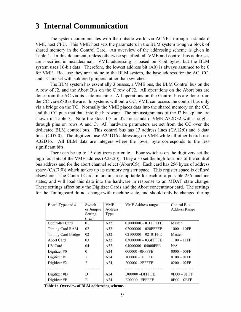
3 Internal Communication The system communicates with the outside world via ACNET through a standard
VME host CPU. This VME host sets the parameters in the BLM system trough a block of shared memory in the Control Card. An overview of the addressing scheme is given in Table 1. In this document, unless otherwise specified, all VME and control-bus addresses are specified in hexadecimal. VME addressing is based on 8-bit bytes, but the BLM system uses 16-bit data. Therefore, the lowest address bit (A0) is always assumed to be 0 for VME. Because they are unique to the BLM system, the base address for the AC, CC, and TC are set with soldered jumpers rather than switches.
The BLM system has essentially 3 busses, a VME bus, the BLM Control bus on the A row of J2, and the Abort Bus on the C row of J2. All operations on the Abort bus are done from the AC via its state machine. All operations on the Control bus are done from the CC via eZ80 software. In systems without a CC, VME can access the control bus only via a bridge on the TC. Normally the VME places data into the shared memory on the CC, and the CC puts that data into the hardware. The pin assignments of the J2 backplane are shown in Table 3. Note the slots 1-3 on J2 are standard VME A32D32 with straight-through pins on rows A and C. All hardware parameters are set from the CC over the dedicated BLM control bus. This control bus has 13 address lines (CA12:0) and 8 data lines (CD7:0). The digitizers use A24D16 addressing on VME while all other boards use A32D16. All BLM data are integers where the lower byte corresponds to the less significant bits.
There can be up to 15 digitizers per crate. Four switches on the digitizers set the high four bits of the VME address (A23:20). They also set the high four bits of the control bus address and for the abort channel select (AbortCS). Each card has 256 bytes of address space (CA(7:0)) which makes up its memory register space. This register space is defined elsewhere. The Control Cards maintains a setup table for each of a possible 256 machine states, and will load this data into the hardware in response to an MDAT state change. These settings affect only the Digitizer Cards and the Abort concentrator card. The settings for the Timing card do not change with machine state, and should only be changed during
Board Type and # Switch or Jumper Setting (hex)
VME Address Type
VME Address range Control Bus Address Range
Controller Card 01 A32 01000000 – 01FFFFFE Master Timing Card RAM 02 A32 02000000 – 020FFFFE 1000 – 10FF Timing Card Bridge 02 A32 02100000 – 02101FFE Master Abort Card 03 A32 03000000 – 033FFFFE 1100 – 11FF HV Card 04 A32 04000000 –04000FFE N/A Digitizer #0 0 A24 000000 –0FFFFE 0000 – 00FF Digitizer #1 1 A24 100000 –1FFFFE 0100 – 01FF Digitizer #2 2 A24 200000 –2FFFFE 0200 – 02FF - - - - - - - - - - - - - - - - - - - - - - - - - - - - - - - - - - - - - - - - Digitizer #D D A24 D00000 –DFFFFE 0D00 – 0DFF Digitizer #E E A24 E00000 –EFFFFE 0E00 – 0EFF
Table 1: Overview of BLM addressing scheme.

10
beam off periods. An important feature of the BLM system is that all abort operations are handled by state machines, once setup by the CC, these operations proceed without intervention from either VME or eZ80. The only things that the CPUs do is setup the parameters. In order to smoothly update the new settings in the DCs and AC, these cards must double buffer all registers with the first register being written via the BLM Control bus. The data is transferred to the actual usage register via a backplane signal Update_Settings which will occur after all settings have been written and will be generated on the TC in response to a command from the CC to be synchronous with the Make_Meas signal.
3.1 Backplane Signal Functions The operation of the digitizer card is controlled by signals on the control bus.
These signals are:
• Reset [C21]: This signal is the BLM Crate reset signal driven by the Controller Card (CC). It resets the state machine on the DC and TC.
• Reset_DC [C20] “Reset Digitizer Card.”: This signal clears the sliding sums and resets the DC raw measurement data (RMD) pointer and TC time-stamp pointer to FFFF. This signal typically is used to initialize the DC and TC and get ready for data taking.
• Make_meas [C22] “Make Measurement”: This signal causes the DC to switch integrator channels, latches the previous abort states, digitizes the reading, resets the integrator, calculates the sliding sums, and makes the abort comparisons. This signal is generated on the Timing Card (TC) and typically runs continuously at about once every 20 microseconds. The sliding sums are made by adding the current reading to the sum and subtracting the oldest reading from the sum. The 3 sliding sums have 3 oldest data pointers, which point to the data in the RMD that is to be subtracted. There is also new data pointer, which sets the location in the RMD where the newest reading is stored. Once the sliding sums are calculated, the state machine might “pre-Fetch” the 3 oldest data readings that will need to be subtracted during the next cycle. When Make_Meas is generated, the TC also stores the real time in the 64k deep time-stamp buffer. Make_Meas triggers the AC to query the abort states of the digitizers.
• Fast_Latch [C15]: This signal is produced on the TC to tell the DC state machine to latch the current Fast_Sum into a register so the controller can read it. The TC latches the time stamp as well. Each of these latch signals also sets a bit in a register and causes the TC to assert the IRQ2 line so that the CC knows to fetch data into its larger circular buffers.
• Slow_Latch [C16]: This signal is produced on the TC to tell the DC state machine to latch the current Slow_Sum into a register so the controller can read it. The TC latches the time stamp as well.
• VSlow_Latch [C17]: This signal is produced on the TC to tell the DC state machine to latch the current Very_Slow_Sum into a register so the controller can read it. The TC latches the time stamp as well.
• Abort_CS(0:5) [C10:14,27] “Abort Channel select”: These signals come from the Abort Controller (AC) and are used to poll all the channels to request abort demand conditions. The DC state machine compares Abort_CS(2:5) with the address switch values to determine if the requested channel is on the board. Abort_CS(0:1)

11
signify channels 0-3 on the board. When selected, each channel’s four abort lines are driven onto the bus’s Abort(0:3) lines. A channel requesting an abort drives the corresponding line low.
• Abort(0:3) [C5:8] “Abort lines 0,1,2,3”: These are the abort requests driven by the DC to the AC in order for the AC to determine how many channels are requesting an abort for each of the four abort types.
• CA(0:12) [A1:12] Control Bus Address”: These are used to address control and data within the state machine. These are driven by the CC.
• CD(0:7) [A19:26] “Control Bus Data”: These are the data lines used to read and write data to and from the state machine.
• MREQ* [A15] “Memory Request”: This active-low signal indicates to the DC, AC, and TC that the CC is sending a valid address on the control bus for them to parse. The eZ80 on the CC uses the same address space for i/o operations as well as memory (i.e. control bus) operations. Thus addresses are valid on the bus only if MREQ* is low.
• MemRD* [A16] “Memory Read”: Indicates that the current Control Bus cycle is a read from the bus by the CC. This is active low and should go down at the same time as MREQ*.
• WE* [A17] “Memory Write Enable”: This is the write strobe for data. Data should be latched on the rising edge of WE*. WE* is pulled low by the eZ80 on the CC (or by the control-bus bridge on the TC).
• Update_Settings [C29]: The abort thresholds, masks and multiplicities are double buffered on the DC and AC with current values and set values. After the CC is notified by the TC of an MDAT event, it updates the set values. When all values have been written, it sets Update Settings to notify the DC and AC to move the set values to be the current values which are then used in abort decisions.
• ITBT_Trig [C2] “Injection Turn-by-Turn Trigger”: Causes the raw data to be written into the 8k ITBT buffer. Once the buffer is full or the system stops, this data is readable via VME. The trigger is caused by the TC receiving the injection marker on BSClk.
• STBT_Trig [C3] “Studies Turn-by-Turn Trigger”: Causes the next 8k raw measurement data to be written into the STBT Buffer. Once the buffer is full or the system stops, this data is readable via VME. Note: that is a STBT trigger happens while an ITBT is in progress, the ITBT is terminated and the STBT operation is initiated. If either of these is in operation a bit is set in a status register and VME is not allowed to read the TBT data. The TC sends ITBT after receiving a programmable TCLK event.
• ChOK [C1] “Channel OK”: Sent by the digitizer to the abort card with the abort data to indicate that the channel is working properly. If ChOK is low, the AC ignores the data and interrupts the CC.
• AIP [C19] “Abort in Progress”: In normal operation AIP is sent by the TC with a programmable delay after receiving the Abort-in-progress TCLK event ($47). AIP on the control bus stops all circular buffers and allows the 64k-deep raw data buffers on the DCs and TC to be read. AIP is latched until reset by external control. AIP can also be set by-hand in the TC.
• IRQ0 [A28] “Interrupt Request 0”: Timing Card notification to Control Card that a TCLK event has been loaded into the TCLK FIFO.

12
• IRQ1 [A29] “Interrupt Request 1”: Timing Card notification to Control Card that an MDAT state change has occurred and the new state is ready to be read.
• IRQ2 [A30] “Interrupt Request 2”: Timing Card notification to Control Card that one or more of the Fast, Slow, or Very Slow latches has fired and the data is ready to read and placed in the circular snapshot buffers on the CC
• IRQ3 [A31] “Interrupt Request 3”: Abort Card notification to Control Card that the AC needs servicing, either it has channel NOT OK bits, or is requesting ABORT.
• CPU_Detect [C23]: Pulled low by CC when plugged into the crate. This disables the control-bus bridge on the TC.
• Error [A32]: Set if any of the cards senses an internal error. This allows the CC to set a VME interrupt to notify the front-end CPU to send an alarm.
• Osc [C31] Oscillator: 10 Mhz from timing card internal oscillator • BusReq [C25] and BusAck [C26]: For future expansion if needed. These allow for a
second master such as a DMA controller to request control of the bus from the eZ80 by pulling the BusReq low, The eZ80 responds by placing all of its control and address lines into a high impedance state and pulling the BusAck low to signal that the requesting device can now use the bus.
3.2 Standard Board ID Block
The BLM system uses a standard scheme for identifying modules. The ID block is found at the lowest VME address for each card. In this way, a crate can be mapped out to verify that the correct cards have been installed in each crate. The ID check also forms a simple test for the basic functioning of each module. The serial number for each board is encoded in a PROM or a serial device such as the DS2401. The structure of the ID block is given in Table 2.
Address Size Function 0000-0001 16 bits Board ID Number (Board type) 0002-01FE 510 characters Board ID Text String (ascii) 0200-0207 64 bits Serial Number from DS2401 etc. 0208-021E 24 bytes Firmware version numbers 0300-0FFE 3.25 kbytes future expansion
Table 2: BLM System Card ID Memory Map

13
Pin Row A Row B Row C Function Write Read Function Function Write Read 1 CA0 C DTA +5V ChOK D A 2 CA1 C DTA Gnd ITBT_Trig T D 3 CA2 C DTA Reserved 1 STBT_Trig T D 4 CA3 C DTA VME-A24 Abort4 (spare) 5 CA4 C DTA VME-A25 Abort0 D A 6 CA5 C DTA VME-A26 Abort1 D A 7 CA6 C DTA VME-A27 Abort2 D A 8 CA7 C DTA VME-A28 Abort3 D A 9 CA8 C DTA VME-A29 Gnd 10 CA9 C DTA VME-A30 Abort_CS0 A D 11 CA10 C DTA VME-A31 Abort_CS1 A D 12 CA11 C DTA Gnd Abort_CS2 A D 13 CA12 C DTA +5V Abort_CS3 A D 14 Gnd VME-D16 Abort_CS4 A D 15 MREQ* C DTA VME-D17 Fast_Latch T D 16 MEMRD* C DTA VME-D18 Slow_Latch T D 17 WR* C DTA VME-D19 V SIow_Latch T D 18 Gnd VME-D20 Gnd 19 CD0 All All VME-D21 AIP T DA 20 CD1 All All VME-D22 Reset DC T DTA 21 CD2 All All VME-D23 Reset C DTA 22 CD3 All All Gnd Make_Meas T DA 23 CD4 All All VME-D24 CPU_Detect C T 24 CD5 All All VME-D25 Gnd 25 CD6 All All VME-D26 BusReq C 26 CD7 All All VME-D27 BusAck C 27 Gnd VME-D28 Abort_CS5 A D 28 IRQ0 T C VME-D29 Spare3 29 IRQ1 T C VME-D30 Update_Settings T DA 30 IRQ2 T C VME-D31 Gnd 31 IRQ3 A CT Gnd Osc 32 Error DTA C +5V Spare2
Table 3: Pin assignments for J2 backplane. The the A and C row, we indicate which modules can read or write data on each of the bussed backplane lines.

14
4 Digitizer Card The digitizer card is the primary data collector in the system. It includes the following
features: • 4 loss-monitor channels, 4 dual integrators, 4 16-bit ADCs • 4 16-bit DACs for analog (MADC) outputs • Control Bus Interface for setting parameters • 512 Kbytes of RAM for storing Raw Measurements Data (RMD) • 128 Kbytes of RAM for storing 2 banks of 8k TBT data • A VME interface used primarily for reading raw measurement data when the
system is stopped and for reading TBT data when TBT is not in operation. • A 4-bit switch-selectable card number that sets the base address for the Control
Bus, Abort Bus and VME. For digitizer cards on the Control Bus, CA12=0 and CA8:11=Switch for card select.
• A state machine that runs the digitizer section and makes the 3 sliding sums for each channel. It also maintains the RMD RAM circular buffer.
• An Abort channel select and 4 abort line drivers, these 4 lines are for: o Immediate Loss Abort threshold (few microseconds) o Fast Loss Abort Threshold (few milliseconds) o Slow Loss Abort Threshold (few 10s of milliseconds) o Very Slow Loss Abort Threshold (few seconds)
The reading of the raw measurement data (RMD) is allowed only when the state machine is stopped, and this data is only available via the VME interface. This is the only data available to VME on this card. The VME Address lines 20:23 are compared with the 4-bit address switch to determine if the card is being addressed. VME Address lines 1:2 are channel select, VME address 0 is byte select (only used if reading in byte mode) and VME address lines 3:18 are the 64k RMD pointer. Note that the RMD is a 64k deep circular buffer used to store raw data; the time stamps for this data are stored on the TC. Both circular buffers start and address offset FFFF and count down. In order to see raw measurement data while running, there are two turn-by-turn buffers that are described below in Section 4.1. VME is also able to read the Card ID Block at 000000 and the board status at 30000.
The internal address map of the digitizer is described in Table 3. These are the offsets from the control-bus base address for data communication with the Control Card.
The response of the digitizer has been calibrated in prototypes. The least count in the low integration range corresponds to a charge of ~0.02pC or a loss of 0.3µRad. In the high range, the least count corresponds to a factor of 5 more charge.
4.1 Turn-by-Turn Buffers In addition to the diagnostic buffers maintained by the Controller Card, which are
circular buffers that are periodically overwritten, the BLM system has two linear buffers in the Digitizer that are triggered and are not automatically overwritten. These buffers are Turn-By-Turn (TBT) and are each 8k deep. The TBT Buffers are designed to match the

15
capability of the new BPM system and allow the simultaneous sampling of beam position in the BPM and beam losses in the BLM.
The injection TBT buffer (ITBT) is designed to match the BPM injection TBT buffer and is triggered by ITBT_Trig at injection. The studies TBT buffer is designed to match the BPM TBT buffer used for beam studies. The STBT is triggered by STBT_Trig, both of these triggers are generated on the TC by clock events on TCLK or BSCLK. When either of these TBT buffers is triggered, the DCs and TC will set a bit in a status register indicating the TBT operations are in progress and that the TBT memory is not accessible from VME. Once the TBT operation completes,or if an abort happens, the DCs and TC will reset the status bit, and VME will have access to the TBT memory.
TBT operations will require the DCs and TC to not only write the large 64k circular buffer each sample period, but to also write the data into the TBT buffer each sample period.
Once it has been triggered, the ITBT will fill to its limit of 16k and stop. It will not be overwritten until another injection clock event happens. If another ITBT_Trig happens, prior to the completion of the ITBT operation, the ITBT pointer will be reset to 0, and 16k of new TBT data will be written into the ITBT buffer. Only the first 8k are protected from an STBT_Trig.
The STBT buffer once triggered, will fill to the limit of 16k and stop. It will not be overwritten until another Studies clock event happens. If another STBT_Trig happens, prior to the completion of the STBT operation, the STBT pointer will be reset to 8k and 8k of TBT data will be written into the STBT buffer.
BLM Digitizer Card
SRAMRaw Data Buffer 64kSamples(Dec)
BLM Input
MADC Out DAC
FPGAControls Integrator
Keeps 3 sliding sums
Maintains RAM Buffer
Does Abort Compares & reports Aborts
Talks to Selectable Data Bus
Does MADC DAC out
1 Channel
Integrator &Signal Conditioning
16 Bit ADC
X 4
VMEBUSJ1A24 D16
Revised 10/11/04
Control Bus A13-D8 on J2
Temperature
ITBTSTBT
Turn-By-Turn8k Buffers(Inc)
J2 Abort Bus A6-D4
Figure 4: Digitizer Card functions

16
If a STBT_Trig happens during an ITBT operation, the ITBT operation is ended and the STBT pointer is set to 0 and an STBT operation is started. Thus only a single TBT operation is allowed at any given time. If this happens the host should be able to fully reconstruct the ITBT data using the ITBT and STBT buffers and their time stamps.
It also possible to provide a software TBT_Trig permit for each type of TBT buffer, so that the buffer could be “locked” and not overwritten unless it is “un-locked”.
4.2 Modes of Operation
The operation of the digitizer can be customized in several ways. These features are controlled via the Mode Select word for each channel. The bits of the Mode Select word are encoded as follows:
0 Enable High Range 1 Enable Long Time Constant 2 Test Mode On 3 Use Integration Mode 6:4 MADC Function Select (2:0) 15:7 Spare
These settings can be changed only when the state machine is stopped. The FPGA Control Register is currently not defined.
4.2.1 High Range The integration capacitor for the integrator chips can be set to either 100pF or 500pF
giving a factor 5 change in the least count and range for the data.
4.2.2 Long Time Constant The normal series resistance of the input to the integrator is about 2kΩ. When the
appropriate control bit is set, and additional 15kΩ resistor is included in series, increasing the effective time constant of the integrator.
4.2.3 Integration Mode The Very Slow Sum can be set as a cumulative integration since the last ResetDC signal. This sum can then be used for the Main Injector to get the integrated loss per machine cycle. At ResetDC the sum is reset to 0x100. Then on each measurement cycle instead of forming the running sum by subtracting the oldest measurement, the current reading is added to the sum and the locally stored pedestal is subtracted. In order to avoid overflows, the internal summing register is 40 bits wide. However, only the upper 32 bits are read out. The Very Slow Latch signal is used to request transfer of the integrated values to the control card.
17
4.2.4 Test Mode In test mode, the on-board DAC is used to send a fixed current to the input of the integrator. The value is set from the Test DAC register.
4.2.5 MADC Function The analog output for each channel can provide up to 8 different signals derived from the
raw data. These are specified in the firmware. The program for the analog output is set via the three-bit MADC Function Select sub-word. The output functions are:
0 Value from MADC Manual Setting 1 Raw measurement value 2 Integrated current value (if enabled)3-7 To be determined
4.2.6 Saturation Protection In order to be sensitive to extremely large losses, the Digitizer protects the integrator
from becoming saturated. During the integration phase of the cycle, the output voltage is checked by a comparator. If it reaches approximately 95% of full scale for the ADC, the input current is shut off, and the remaining charge is stored on the cable. Thus for large losses, the leading edge time is preserved; however, the raw measurement will be near full scale until all charge from the loss has been collected. Those measurements will be included as normal in the sliding sums. In this way, by summing over measurements, it is possible to record the full energy deposition.
4.3 Pedestals All digitizers measurements are positive integers. In order to avoid bias from negative
noise signals, a fixed current is added to the input of each integrator circuit. This presents a pedestal for each measurement. As discussed in section 4.2.3, a pedestal is subtracted in making the integrated sum. However, for the raw measurement data or sliding sum data, pedestals must be subtracted external to the digitizer. In order to minimize the load on the control card, these subtractions should be done by the front-end CPU. Abort thresholds for each channel should be stored in the Acnet database to correspond to actual losses and should be corrected for the pedestals by the front end before loading them to the Control Card. The current injection and gain of the integrator circuit should be sufficiently stable that calibrations will need to be taken only infrequently. The simplest procedure is to take data with no beam in the machine and average the data from a large fraction of the Fast Sum circular buffer. The pedestal for the raw data and for the other running sums can be formed by correcting for the appropriate sum length. While care will be taken to minimize analog noise, some residual 60Hz and 720Hz noise will remain. Therefore, the length of the averaging period used to determine the pedestal should be an integral multiple of 1/60 second. For the Tevatron, this is 795 cycles; while for the main injector, it is 748 cycles at 8 GeV with Make_Meas running at half the AA marker frequency.
Because the on-board pedestal must be an integer, it is possible to see a slow drift in the integrated measurement with no losses. In the low (high) range this is 14 mRad/s (70

18
mRad/s).
4.4 VME Address Map
BLM digitizer cards respond to A24D16 and may take nearly all of the A24D16 address space (16 MB) since there may be up to 15 digitizer cards. Each card uses the addresses N00000-NFFFFE where N is card number 0-E. The base address is set by switches on the board which determine bits 20-23. The data are stored as follows as offset from the base address.
• 00000-00FFE Standard ID block (sec. 3.2) • 10000-1FFFE 64KB of Injection TBT Data (8k Turns, Increments) • 20000-2FFFE 64KB of Studies TBT Data (8k Turns, Increments) • 30000 Status Register • 80000-FFFFE Raw Measurement Circular Buffers (64k turns)
The turn-by-turn linear buffers and raw circular buffers are addressed as follows: • A2:A1 = Channel 0/1/2/3 • A18:A3 = Index
The index for the raw buffer is set to FFFF on a reset and decrements on each Make_Meas. It resets when it reaches 0000. The current location is indicated by the RMD pointer which is located in the settings block that is yet to be documented.
VME DC and TC Status RegisterRevised 10/14/04
Bit 15 Bit 0Bir 7Bit 8
AIP RunningTBTActive
TCLKActive
Bit 15 Bit 0Bir 7Bit 8
AIP RunningTBTActive
DC
TCBSCLKActive
MDATActive
Figure 5: Digitizer and timing card status registers.

19
Function Type Address Bytes Bits
Channel 0 00 (36) Fast Sum Threshold R/W 00 4 32 Slow Sum Threshold R/W 04 4 32 Very Slow Sum Threshold R/W 08 4 32 Immediate Threshold R/W 0C 2 16 Fast Sum Latched R 10 4 32 Slow Sum Latched R 14 4 32 Very Slow Sum Latched R 18 4 32 Mode select R/W 1C 2 16 MADC Manual setting R/W 1E 2 16 Current reading R 20 2 16 Pedestal R/W 22 2 16 Channel 1 (36) Fast Sum Threshold R/W 30 4 32 Slow Sum Threshold R/W 34 4 32 Very Slow Sum Threshold R/W 38 4 32 Immediate Threshold R/W 3C 2 16 Fast Sum Latched R 40 4 32 Slow Sum Latched R 44 4 32 Very Slow Sum Latched R 48 4 32 Mode select R/W 4C 2 16 MADC Manual setting R/W 4E 2 16 Current reading R 50 2 16 Pedestal R/W 52 2 16 Channel 2 60 (36) Channel 3 90 (36) General F0 Fast Sum Length R/W F0 2 16 Slow Sum Length R/W F2 2 16 Very Slow Sum Length R/W F4 2 16 TBT Ram Pointer R F6 2 16 FPGA Control Register R/W F8 2 16 Test DAC R/W FA 2 16 ADC Temperature R FC 2 16
Table 4: Digitizer Card internal register map

20
5 Timing Card The timing card (TC) is the primary controller for data collection in the BLM
system. It includes the following features: • Control Bus Interface for setting parameters • A TCLK decoder. This is used to receive the encoded TCLK events such as Clock
Reset, Abort-in-Progress, and Profile requests. Receiving a TCLK event causes IRQ0 to be asserted. A 1 MHz clock is derived from this clock. In locations without a TCLK, an optional 10 MHz oscillator is provided. The list of interesting TCLK events is stored in registers. The TC loads the events in a FIFO for the CC to read.
• A BSCLK decoder. This is used to receive the encoded Beam-Sync Clock events such as $AA. This AA marker is optionally used to make the Make_Meas signal. Make_Meas can also be derived by dividing the AA marker such as for Main Injector where Make_Meas is AA/2.
• An MDAT decoder. This is used to receive machine state information from the MDAT system. Different machine states require different abort thresholds etc. Receiving an MDAT event causes IRQ1 to be asserted. The MDAT frame of interest is set in a register. For the Tevatron, it is $12. An MDAT event is defined as a change in the value of the relevant frame. Only the lowest 8 bits of the frame are considered.
• A real-time clock. The 32-bit Unix time in seconds is incremented by the TCLK 1 Hz event ($8F). A 24-bit microseconds counter increments from each 1 Hz event. These time values are used to mark the digitizer raw and sum data.
• 512 Kbytes of RAM for storing 64k of Raw Measurements Data Time Stamps (RMDTS) these are stored as 8 bits of state, 32 bits Unix time in seconds, and 24 bits of microseconds.
• 128 Kbytes of RAM for storing TBT time stamps. • A VME interface used for reading RMDTS when system is stopped and for reading
TBT Time Stamps when TBT is not in operation. • Make_Meas backplane output. Make_meas can be generated from either of two
sources: o The1 MHz clock with an 8-bit divisor o The AA marker from BSClk, or from the AA Marker /2 for MI.
The Make_Meas signal also latches the 64-bit time-stamp data and writes it into the RMDTS ram array and increments the RAM Pointer. The Reset_DC signal resets this pointer.
• Divisors of the Make_Meas signal used to make the Fast_Latch, Slow_Latch, and Very_Slow_Latch signals. The divisors are 16 bit numbers. These latch signals set a bit in a register and cause IRQ2 to be asserted so that the CC knows to read the latched data from the digitizers. These three latch signals also latch the current time stamp into three registers so that the time stamp can also be read.
• Writeable registers to force the creation of Reset_DC, AIP, Clear AIP etc • Front Panel lemo inputs which also make Reset_DC, AIP, and Clear AIP • Abort-in-Progress (AIP) signal. AIP being asserted causes the state machine to stop
Figure 6: Timing Card functional overview

21
making all control pulses: Make_Meas, xxxx_Latch, etc., effectively freezing all buffers in the system. AIP is a latched signal cleared by Clear_AIP and by Reset.
• ITBT Trigger. This line is driven onto the backplane in response to a BSCLK Injection clock event, it causes the 8k Injection TBT buffer to be filled on the digitizer cards as well as the injection TBT time stamps to be filled on the TC.
• STBT Trigger. This line is driven onto the backplane in response to a TCLK Studies clock event, it causes the 8k Studies TBT buffer to be filled on the digitizer cards as well as the Studies TBT time stamps to be filled on the TC.
The internal registers for the Timing Card are described in Table 7. The Timing
Card is controlled by signals on the control bus and by TCLK, BSCLK, and MDAT events. The reading of the Raw Measurement Time Stamp (RMDTS) circular buffer is
allowed only when the state machine is stopped, i.e. AIP is true. The TBT time stamp buffers can be read whenever a turn study is not in progress. The address map is described in section 5.1 below.
The TC also includes a VME to Control Bus Bridge to allow for setting up the DC and TC hardware in situations where a CC module is not present. VME Address line 20 set to 1 indicates that the Bridge is being accessed. VME Address lines 1:13 are copied to Control Bus address lines 0:12 and control bus data lines 0:7 are connected to VME data lines 0:7. The bridge must also use appropriate VME signals to create the following Control Bus signals: MEMRD*, MREQ*, and WE*. The TC will pull Bus line CPU_Detect high. If this line is sensed low, the bridge will be disabled since there is a CC
BLM Clk and Timing CNTL CardTeV Clk Decoder
NovRam
FIFO
1HzAIP Latched
IRQ0
10 MHzOsc
cBUS
TBT Studies
32 Bit CounteruSec Count
24 Bit Counter
Sec Count
RAM TBT Time stamps 64 Bits x 64k
SnapShot Time stamp latch 64 Bits
1 Hz 1 MHzClk ResetcBUS
FastLatch
SampleState 8bits
Slow SnapShot Time stamp latch 64 Bits SlowLatch
Very SlowSnapShot Time stamp latch 64 Bits VslowLatch
cBUS
cBUS
cBUS
cBUS
VME BUSReset DC
Ijectiopn TBT Time stamps 64 Bits x 8k
Studies TBT Time stamps 64 Bits x 8k
Control Bus A13-D8
VME J1 A32-D16
VME CNTL Bus Bridge
Revised 10/12/04
Clock Devisor10 MHz
Clk Reset
Meas Divisor 8bits
Fast Divisor 8 bits
VSlow Divr 16 bits
Slow Divisor 16 bits
Injection TBT
Sample
SlowLatch
VslowLatch
FastLatchSample
1 MHz1 Hz
cBUS
cBUS
cBUS
cBUS
IRQ2
BSClk
AA
AA
Update Settings
MDat Decoder
NovRam
FIFOIRQ1
cBUS

22
present. To set the seconds counter, one writes the time setting to the appropriate registers
and then sets the register to update the time setting on the next $8F TCLK event. The TC resets that register when the time has been updated. When using a host CPU to set the time on the Control Card, there is a similar feature whereby one sets the time to use in the update and sets a register that the CC polls periodically to see if there is an updated setting to pass to the TC.
5.1 VME Memory Map
BLM Timing Cards respond to A32D16 and takes 2Mb. Each card uses the addresses N000000-N1FFFFE where N is the base address. The base address is set by switches on the board which determine bits 24-31. The default value is 0x0010. The data are stored as follows as offset from the base address. • 00000-00FFE = Standard ID Block (sec. 3.2) • 10000-1FFFE 64KB of TBT Data (8k Turns) Injection, linear buffer • 20000-2FFFE 64KB of TBT Data (8k Turns) Studies, linear buffer • 30000 Status Register • 80000-FFFFE 512KB of TBT Data (64k Turns), Circular buffer • 100000-103FFE VME to CNTL Bus Bridge
The time data is encoded as follows
• A2:A1 = Time Stamp Words (0-3) • A18:A3 = Turns number
The structure of the data is:
Word Byte 0 Byte 1 0 Microseconds, byte 0 Microseconds, byte 1 1 Microseconds, byte 2 MDAT State 2 Unix Time, byte 0 Unix Time, byte 1 3 Unix Time, byte 2 Unix Time, byte 3
For the 64k turns of raw measurement data, the index decrements from FFFF to
0000 and wraps when it reaches 0000. This data can be read only the system is stopped (i.e. AIP is true). The timestamps for turn-by-turn data may not be read during a turn study.
When using the control bus bridge VME A13:1 map to CA12:0, and A19:14 are ignored. The 8-bit Control bus data is on VME D7:0

23
Function Type Address (Hex)
Bytes Bits
Setup CSR R/W 00 2 16 State Number R/W 02 1 8 Status R 03 1 8 Seconds Time Clock setting W 04 4 32 Set Clock on next ($8F) 08 1 0 Update Settings on next Make_Meas 09 1 0 MDAT Frame ID R/W 0A 2 16 TCLK or BSCLK Number R/W 0C 1 8 TCLK Prom Setting W 0D 1 8 BSClk Prom Setting W 0E 1 8 Control Make_Meas Divisor R/W 10 1 8 Immediate Sum Length R/W 11 1 8 Fast Sample Length R/W 12 1 8 Slow Sample Length R/W 14 2 16 Very Slow Sample Length R/W 16 2 16 TBT Ram Pointer R 20 2 16 TCLK Event FIFO R 30 1 8 BSCLK Event FIFO R 31 1 8 MDAT Event FIFO R 32 2 16 Clocks/Timing Fast Latch Time Stamp R 40 8 64 Slow Latch Time Stamp R 48 8 64 Very Slow Latch Time Stamp R 50 8 64 General Force Clear W F0 1 0 Force Start (Reset DC) W Fl 1 0 Force Stop W F2 1 0 Force ClkReset ($8F) W F3 1 0 Force AIP W F4 1 0 Force Sum Latches W F5 1 0 Force ITBT Trigger W F6 1 0 Force STBT Trigger W F7 1 0 IRQ2 Status Reg Fast R/W=Clr F8 1 0 IRQ2 Status Reg Slow R/W=Clr F9 1 0 IRQ2 Status Reg Very Slow R/W=Clr FA 1 0 Diagnostics ADC Temperature FE 2 16
Table 5: Timing Card internal register map. The address is the offset from the control-bus base address.

24
6 HV Card The High Voltage card is a double-wide 6U VME module that can carry one to four
high voltage modules that are independently controlled through the VME bus. It has an 8-bit switch selectable card number which sets the card address corresponding to VME address (A31:A24). A Quad 12-bit DAC provides the program voltage for each of the high voltage modules for voltage output control. The combination multiplexer and 16-bit ADC reads the high voltage monitors for each module.
The card incorporates an FPGA (Altera Cyclone) to interface with the VME bus, local timing and control. The FPGA receives all the VME bus control, address and data lines for read/write of data on the card. The FPGA can be programmed from the front panel through the Active Serial Program connector. The card has a serial number and ID memory to identify individual cards.
The program voltage circuitry consists of a 12-bit four-channel DAC device and an op-amp gain circuit. The DAC is controlled from the VME bus through an FPGA to select and send data to the selected channel. The DAC accepts straight binary (0 to FFF) which corresponds to a program voltage output of 0 to 10V. The high-voltage is linear in the setting value with a maximum value of 2250V.
To read all the high voltage monitors, the card uses a 16-to-1 multiplexer and 16-bit unipolar input digitizer. The circuit operates in a circular mode, such that the digitizer is continuing digitizing all the monitor signals from each channel and storing the data into registers. The registers then can be read at anytime through the VME bus. The ADC has an input range of 0 to 3.33V with an output of straight binary (0 to FFFF). The timing and control is done through the FPGA.

25
6.1 Address Map The base address is given from a dip switch which corresponds to A31:A24. The
address offsets for the data are as follows:
Offset Function 00-3E Board ID 42-46 Serial Number 50 Channel 1 HV Setting 52 Channel 1 Output Current 54 Channel 1 Output Voltage 56 Channel 1 Return Voltage 60 Channel 2 HV Setting 62 Channel 2 Output Current 64 Channel 2 Output Voltage 66 Channel 2 Return Voltage 70 Channel 3 HV Setting 72 Channel 3 Output Current 74 Channel 3 Output Voltage 76 Channel 3 Return Voltage 80 Channel 4 HV Setting 82 Channel 4 Output Current 84 Channel 4 Output Voltage 86 Channel 4 Return Voltage 90 Enable/Disable HV (4 bits)
The only data that can be written are the HV settings and the HV enable words. Note
that only the lowest 12 bits are significant in the HV setting.

26
6.2 Positive High Voltage Module (+2kV)
The High Voltage module is a self-contain module with two SHV connectors, one for high voltage output, the other for a high voltage return. A third connector is used as an I/O for input power, program voltage and high voltage monitoring. High voltage is produced by a dc to high voltage converter that is controlled by a programmed voltage input. The high voltage output is regulated and has low ripple output. The module also has three high voltage monitors for voltage output, voltage input return and current output monitoring. Shown below are the specifications for the module.
• DC to HV Converter: 0 to 3000V @ 500µA max. Emco model: G30 • Voltage Output: 0 to +2.25kV • Maximum current output: 500µA • Output Ripple: < 200mVp-p (full load) freq. @ 150KHz • Output Regulation: < .1% @ full load • Program input voltage: 0 to +10V • Voltage & current inputs: +12V @ 220mA, -12V @ 5mA (full load) • Monitor outputs:
o HV current monitor: +1V/100uA o HV output monitor: +1V/1000V o HV return monitor: +1V/1000V
• Status monitor (on/off): ON = +3.3V, OFF = 0V • HV input and output connectors: SHV, Kings No. 1704-1 • I/O connector: AMP 534237-8 • Module size: L 5” x W 2” x H 1.125”

27
7 Abort Card The Abort Card (AC) is the primary controller for abort collection and reporting. The
BLM abort status will be sent to the existing abort chassis in each service building. In addition, each card will be part of a serial link which sends Tevatron abort information from house to house to a dedicated collection board located at A0. A diagram of the abort cards data flow is given in Figure 7. Functions and features of the abort card are as follows:
• Reads the Abort information from each Digitizer Card once per measurement cycle. • Applies channel mask and multiplicity requirements before requesting an abort. • Stores the abort information in a VME-readable circular buffer for 65536 turns. • Periodically sends this abort information to the next house, forming a serial data
stream of abort information. Each successive house appends its data to the data stream.
• VME registers exist for reading the circular buffer, testing the memory, sending diagnostic signals, reading board ID information.
• Control Bus for setting the mask and multiplicity values, and for reading the Channel OK bits that were latched while reading abort information from the DCs.
• Abort bus for reading the abort bits from the Digitizer Cards. • Masks and Multiplicity numbers are double-buffered.. • Front Panel Lemo outputs: Immediate Abort, Fast Abort, Slow Abort, Very Slow
Abort. • Front Panel BNCs: Abort Out, Serial Link In, and Serial Link Out.. • VME Test of Serial Link • VME interrupt capability to be specified. • Front panel displays and LEDs show the board status. • Remote FPGA programming capability using the VME bus
The Abort Card is master of the Abort Bus, which is used to gather abort data for
the crate. Upon receiving a Make_Meas signal, the Abort Card sends addresses out on the AbortCS[5..0] and for each address sent it receives one channel’s worth of abort data on the Abort[3..0] lines. These four bits correspond to the four “abort types” Immediate abort, Fast Abort, Slow Abort, Very Slow Abort. If a bit is a “0” then the channel has a digitized value greater than its threshold value (preset in the Digitizer Card via the Control Bus). AbortCS[5..3] represent the DC board address, and AbortCS[1..0] represent the four individual channels per board. Upon receiving all the abort information, the Abort Card counts the number of channel hits per abort type and compares the value to a preset multiplicity value. If any value is greater than the multiplicity threshold the AC sends an abort request to the Abort System via a BNC connector on the front panel. Each of the four abort types behaves independently in this manner, and four Lemo connectors exist on the front panel in case individual pulse information is desired. The abort outputs are active-low. Thus the TTL high output corresponds to a beam permit.
Each digitizer channel in the crate can also be “masked” to prevent its inclusion in an abort request. There are four masks per channel corresponding to the four abort types.

28
• Abort 0 Immediate Abort • Abort 1 Fast Abort • Abort 2 Slow Abort • Abort 3 Very Slow Abort.
A mask setting of “1” allows that channel to cause an abort. The abort bus also includes a Channel OK line. This indicates that the digitizer
state machine is functioning properly. In case of an error, the abort card keeps a mask of problem channels and can interrupt the control card to generate an error associated with the problem. If a CHOK is false, the channel is not used in the abort multiplicity calculation.
The register map for control bus data is given in Table 7.11
Memory Pointer (Bits 11..04)
R 02 1 8
Memory Pointer (Bits 19..12) R 03 1 8 Interrupt Register R A6 1 7 Abort Status Register R A7 1 5 Abort Snapshot Register R/W 60 32 256 Abort OR Register R 80 32 256 Snapshot Pointer (Bits 11..04) R 04 1 8 Snapshot Pointer (Bits 19..12) R 05 1 8

29
7.1 Table

30
7.1 Control Bus Memory Map Function Type Address Bytes Bits Masks Abort Mask R/W 00 1 6 Abort Channel Count R/W 01 1 6 Abort Enable R/W 0A 1 1 Immediate Abort Mask R/W 10 8 64 Fast Abort Masks R/W 18 8 64 Slow Abort Masks R/W 20 8 64 Very Slow Abort Masks R/W 28 8 64 NA (Formerly “New Abort Masks”) 30 8 64 Multiplicities Immediate Multiplicity R/W 40 1 6 Fast Multiplicity R/W 41 1 6 Slow Multiplicity R/W 42 1 6 Very Slow Multiplicity R/W 43 1 6 NA (Formerly “New Multiplicity”) 44 1 6 General Force Abort H R/W 45 1 6 Force Abort L R/W A4 1 6 Force Abort Permit R/W A5 1 6 Diagnostic ADC Reading Temperature R 4E 2 16 Channel OK R 50 8 64 Memory Pointer (Bits 11..04) R 02 1 8 Memory Pointer (Bits 19..12) R 03 1 8 Interrupt Register R A6 1 7 Abort Status Register R A7 1 5 Abort Snapshot Register R/W 60 32 256 Abort OR Register R 80 32 256 Snapshot Pointer (Bits 11..04) R 04 1 8 Snapshot Pointer (Bits 19..12) R 05 1 8
Table 7.1.1: Control Bus register map for Abort Card
Bit Interrupt Register Abort Enable Abort Mask Abort Status 0 Assert IRQ3 when an abort occurs
before multiplicity is applied Abort Enable Immediate Immediate
1 Assert IRQ3 when an abort occurs Zero Fast Fast 2 Assert IRQ3 when any Channel
“not OK” Zero Slow Slow
3 Zero Zero Very Slow Very Slow 4 Raw Abort Interrupt Two consecutive aborts 5 Abort Interrupt Zero All Logical OR 6 Ch not OK Interrupt Reset Abort OR Register 7 Clear IRQ3 Zero
Table 7.1.2: Control Bus register bits The Abort Snapshot register captures the last frame of the Abort History circular buffer just prior to an abort. See tables 7.2.3 to 7.2.5. It will keep this frame until anything is written to register 1160. The Abort OR register keeps a running tab of which abort bits went over threshold since the last reset. This reset is bit D6 of the Abort Enable register or power-up or Reset CB. The Abort OR register does not register the “sum words” that exist in the circular buffer.

31
7.2 VME Memory Map The base address of the ACs in the field is 12000000. The base address of the ACs in the test stand is 03000000. The address offset and data for the Abort Card are as follows:
00A000, 00A002 JTAG programming and enable registers 000000-000FFE 8kB of Settings, ID etc. 020000 Interrupt Register 030000 Abort Status Register 040000 Memory Pointer LSBs 040002 Memory Pointer MSBs 050000 Memory Test Register 050010 Abort Control Register 060000 Serial Diagnostic Register 060010 Serial Link Test Register 070000 Position in Serial data stream (reserved) 200000-3FFFFE Abort History Circular Buffer (64k turns)
Table 7.2.1: VME Bus register map for Abort Card
The bits of the various settings and status registers are decoded according to the following table: Bit Interrupt Register
(reserved) Abort Status Register
Memory Test Register
Serial Link Test Register
Abort Control Register
0 R/W Running Memory Test Mode (allows VME write cycles to Circular Buffer)
Error Count Bit0
Reset for VME and CB Registers
1 R/W Circular Buffer “Wrapped” bit
Zero Error Cnt Bit1 Zero
2 R/W Immed. Abort Zero Error Cnt Bit2 Zero 3 R/W Fast Abort Zero Error Cnt Bit3 Zero 4 R/W Slow Abort Zero Error Cnt Bit4 Serial Link Reset 5 R/W V. Slow Abort Zero Error Cnt Bit5 Zero 6 R/W Zero Zero Error Cnt Bit6 Zero 7 R/W AIP Zero Error Cnt Bit7 Zero 8 N/A Reset Abort
Status R Error Cnt Bit8 N/A
9 N/A N/A N/A Error Cnt Bit9 N/A
10 N/A N/A N/A Error Cnt Bit10 N/A
11 N/A N/A N/A Error Cnt Bit11 N/A
12 N/A N/A N/A Error Cnt Bit12 N/A
12 N/A N/A N/A Error Cnt Bit13 N/A
14 N/A N/A N/A Reset Err Count N/A 15 N/A N/A N/A Link Test Mode N/A
Table 7.2.2: Definition of bits for VME Registers

32
The Abort History is a circular buffer parallel to those in the Digitizer and Timing cards. Each data record frame is 32 bytes, and corresponds to one turn. The first 28 bytes contain the unmasked abort status for 56 of the 64 possible DC channels in a crate. A 16-bit status word for four channels is structured as follows:
Bit Channel Status 0 0 Immediate 1 0 Fast 2 0 Slow 3 0 Very Slow 4 1 Immediate 5 1 Fast 6 1 Slow 7 1 Very Slow 8 2 Immediate 9 2 Fast
10 2 Slow 11 2 Very Slow 12 3 Immediate 13 3 Fast 14 3 Slow 15 3 Very Slow
Table 7.2.3: Definition of bits for each 16-bit word in the circular buffer The Abort History data record has the following structure; channels are numbered
commensurate with backplane lines AbortCS[5..0]:
Offset Function 0 Status, Channels 0-3 2 Status, Channels 4-7 4 Status, Channels 8-11 ……. ………………. 1A Status, Channels 52-55 1C Summary word 1 1E Summary word 2
Table 7.2.4: VME address offset corresponding to DC channels
The two summary words contain the multiplicities of the aborts after the mask and the abort bits that are output to the beam-permit system:
Word Bits Function 1 0:3 Abort bits (VS, S, F, I) 1 4:9 Fast Abort Multiplicity 1 10:15 Immediate Abort Multiplicity 2 0:3 4-bit counter incrementing on MM 2 4:9 Very Slow Abort Multiplicity 2 10:15 Slow Abort Multiplicity
Table 7.2.5: Last two words in each circular buffer frame (one frame per turn)

33
7.2.1 Abort Status Register The Abort Status Register looks at the status the four abort bits as seen on the front panel, except they are latched in this status register to record if any bits had gone high and subsequently cleared. This was intended as a tool for the Operators to keep track of aborts around the ring. The reset Abort Status bit resets only the four abort bit readbacks in this register. Actually any write to this register will perform the reset. These bits do not affect the front panel outputs. The bits are also cleared by Sysreset, front panel reset, and bit D0 of the Abort Control Register.
Also in this register is “running” which is the inverse of AIP, and the Circular buffer “wrapped” bit. The Wrapped bit is cleared by a front-panel reset or the backplane signal Reset DC. 7.2.2 Remote FPGA programming The Abort Card’s three FPGAs are normally programmed by connecting a cable called a “ByteBlaster” between the parallel port of a computer and the JTAG connector on the front panel of the Abort Card, and running the proper programming file using Altera’s Quartus program into the Abort Card’s configuration device. The configuration device holds the FPGA programming bitstream in non-volatile memory, and programs the FPGAs whenever the board is powered-up. An alternative method of loading the configuration device exists using four bits of a VME register to emulate the four bits of the JTAG lines. The following table shows the bit assignments.
Bit JTAG Function
D0 TCK
D1 TMS
D6 TDI
D7 TDO
Table 7.2.1.5: VME register 00A000 for loading the configuration device
This programming register is at 1200A000. As a precaution, in order for this programming operation to occur, a special code must be written to register 1200A002. Currently the only requirement in this special code is that a 1 be written to bit D0. The idea is obviously to ensure that no random or erroneous VME operations corrupt the FPGA configurations. The special code is cleared in one of five ways: Removing the special code in register 1200A002 Writing Abort Control register 12050010 bit D0 high (Abort Card general reset) Pressing Front Panel reset VME System reset Power-cycle
The software routines for carrying out the remote programming will be provided.

34
7.2.3 Reset Functions A breakdown of the reset functions of the board follows: Front Panel Reset Button: VME State Machine, VME Interrupt Register, Control Bus sequencing, CB Interrupt Register, Abort Outputs, Abort enable bit, Snapshot register, wrapped bit, circular buffer pointer, all Serial state machines and FIFOs, Serial error detector. VME SysReset: VME State Machine, VME Interrupt Register, Control Bus sequencing, CB Interrupt Register, Abort Outputs, Abort enable bit, Snapshot register, all Serial state machines and FIFOs, Serial error detector. Abort Control Register Bit D0: VME Interrupt Register, AbortStatusRegister, MemTest Register, JTAG programming registers, Control Bus sequencing, CB Interrupt Register, Abort Outputs. Abort Control Register Bit D4: All Serial state machines and FIFOs, Serial error detectors. Reset DC (backplane): Wrapped bit, circular buffer pointer, Snapshot register. Reset CB (backplane): Abort enable bit, Snapshot register.
7.3 Abort Card at A0 (preliminary) A special Abort Card at A0 is used for initiating the Serial link data stream and processing all the houses’ data from the serial link once they make it completely around the ring. All three FPGAs on this abort card need special firmware. Although the data is serialized for transmission on the buried coax between houses, the Serial Link FPGA on each Abort Card treats the data a byte at a time. Upon receipt of the signal “Abort Sync” from the Timing Card, A sixteen byte “preamble” is sent out of the A0 card to the first house, A1. This house checks for the correct preamble and puts its 32 bytes of data immediately at the end of the preamble and sends out the data to A2. Each subsequent house tacks its 32 bytes of data immediately onto the end of the data from the upstream house until the whole ring’s worth of data arrives back at the A0 Abort Card. The A0 card largely ignores the four sum bytes from each house, separates out the bits based on abort type, adds up the bits and compares these four sums to serial-link multiplicity values also based on abort type. If any are over threshold, and also “enabled”, an abort signal goes out the front panel. The Abort Sync occurs every 2 msec.
7.3.1 Abort Multiplicity Registers There are four abort multiplicity settings, one for each abort type. 14A00000 Bits D[7..0] Immediate multiplicity 14A00000 Bits D[15..8] Fast multiplicity 14A00002 Bits D[7..0] Slow multiplicity 14A00002 Bits D[15..8] Very Slow multiplicity

35
7.3.2 Abort Enable Register The abort Enable register (14A00004) allows individual inclusion of each abort type from around the ring to be included in the ringwide abort signal. There is also a bit for ignoring the “Abort Sync” pulse on the backplane, used when you want to read the contents of the serial link data buffer (normally this buffer is stable only after an abort).1 Bit D6 is a flag indicating an error has been detected in the preamble of the serial data returning from around the ring. Bit D7 is a flag if an abort resulting from the serial data has occurred. Writes to bits 6 and 7 also reset their respective flags.
Bit Abort Enable 0 Immediate abort enable 1 Fast abort enable 2 Slow abort enable 3 Very Slow abort enable 4 Zero 5 Inhibit “Abort Sync” (for diagnostics) 6 Preamble Error Read and Reset Error 7 Abort Read and Reset Abort
Table 7.3.1: A0 Abort Enable register bits
7.3.3 A0 Serial Link Data Buffer The A0 Serial Link Data Buffer (14060000) is a FIFO memory that stores the complete data set that makes it to A0 prior to the latest abort. The data is comprised of all 32 bytes of circular buffer data from each house, including sum words, for a total of 880 bytes (16 byte preamble + 27 houses x 32 bytes). Data order is the preamble from the A0 Abort Card, A1 data, A2 data, and so on. To obtain this data, read 14060000 a minimum of 880 times. As long as Abort Syncs are occurring, this buffer will accumulate data, writing over the previous ring’s worth of data with each Abort Sync. When an abort occurs the buffer will continue filling until it receives all the data fromn the last house in the chain. Further writing is then prohibited. The buffer is re-armed when bit 7 of the Abort Enable register is written high. See above section for reading this data when there are no aborts.
7.3.4 A0 Serial Link Error Handling The Serial Link Receiver on each Abort Card checks for valid 8B/10B data arriving at the input. If an invalid code is detected an error bit is generated. This error bit is placed on bit D3 of the last of the four sum bytes in the serial data (it does not affect the counter in the circular buffer described above). This bit is the exception; the rest of the bits in the four sum bytes from each card are ignored by the A0 Abort Card. If this bit is set from any of the ACs in the ring, it is assumed that the data for the present sample prior to this point is wrong and the serial link multiplicity counters are reset, 1 Please note that a similar bit for ignoring Sync Pulse exists for all “normal” ACs: bit D15 of register12070000. These bits reset to “inactive” at power-up.

36
preventing an abort. Error free transmission after this point in the turn may still abort if there are enough bits set. Upon receiving the next Abort Sync pulse from the TC, the algorithm starts anew. A register at 14070000 is available for reading the number of errors detected around the ring. A fourteen bit number counts the errors between resets to the register. The number resides in bits D13-D0, and the reset is bit D14. To date, no errors have been detected on the link. A similar register which monitors only the errors from the upstream house resides at 14060010. It is also has a fourteen bit counter and is reset by bit D14.

37
8 Controller Card The Controller Card (CC) is the primary controller for the Tevatron BLM system. It
includes the following features: • Control Bus Interface Master for setting parameters and reading back sliding
sums, etc. • A 8 Megabyte Block of shared memory with the VME bus, this is used for
getting setup parameters and for storing the circular buffers and other frame memories.
• Two RS-232 ports for diagnostics and standalone operation • A TCP/IP 10/100 baseT port for standalone operation.
8.1Data Structures BLM data is reported in two different ways: Snapshots and Profiles. A profile is taken in
response to a TCLK event. Profile data are the most recent data from the Fast Sum (typically 1ms) from each BLM channel. The “Flash” and “Display” frames are the same as a Profile, but are taken in response to a different TCLK event. In order to make a smooth transition from the legacy system, all three types of events are retained. It is possible to store up to 256 Flash frames and 256 Profile frames in the CC for later readout and analysis. There is only one Display Frame. The current frame indexes are stored in registers. The Snapshot buffers contain the history of losses for all channels for data from each of the sliding sums. These data are stored in the circular buffers of the Control Card and can be read by the front-end CPU from the CC’s dual-port memory and then reported to ACNET. Snapshot data is stored in the same format as the Profile data and is essentially
Control Bus A13-D8
VME J1 A32-D16
BLM Controller Card
FPGA/CPLD*eZ80
256k 8 MegabytesData Buffers& Status
Settings*FUBARPreventing
Good AlternativeC Programming is
LameDude
Revised 10/11/04
Temperature
MDat Decoder
NovRam
FIFOIRQ1
cBUS
Figure 7: Control Card block diagram

38
circular buffers of the same data events. In addition to the sliding sum data, Profile/Flash/Display events include the integrated loss since the last reset (see Section 4.2). Thus these data records are 512 bytes long, while the Snapshot (circular buffer) records are only 256 bytes long. Note that the integrated loss is written only for the Main Injector. In the Tevatron where the Very Slow Sum is used, the integrated values in the Profile frames are zeroes, but the frame format is unchanged.
A BLM data entry has the following format Byte Offset
Length Function
0 1 Machine state (0-255) 1 1 Measurement Divisor 2 2 Sum Divisor 4 1 Abort Status 5 1 Channel Count 6 2 Spare 8 4 Time stamp: Microseconds since
last TCLK 1 Hz Event C 4 Time stamp: seconds since T0
(i.e. 1 January 1970) 10+n*4 240 Sliding Sum data for channel n 100 16 Unused 110+n*4 240 Integrated data for channel n
In the abort status word, bits 0-3 are the status of the abort from the Immediate, Fast,
Slow, and Very Slow measurements, respectively. Bits 4-7 are not used. Loss data are stored as a 32-bit word with data in order from least significant to most significant byte.

39
7.4 BLM Controller Card Memory Map (8 MB)
The controller card has the shared memory in the system, and thus contains all settings and parameters as well as the large circular buffers.
A24-31=jumper setting, default = 00000001 ID Block for CC is at 01000000-01000FFE A32-D16 (01800000-01FFFFFE) All addresses are added to card base address. Dual Port Begins at 1800000. Addresses described below are added to this address. The
channel number (0-59) is trivially derived from the d*4+i where d is the digitizer number and i is the channel within the digitizer.
7.4.1 System Status 000000 System Status (to be defined) 000012 Time Setting Ready (see Sec. 5) 000014 Time Setting 16 LSb 000016 Time Setting 16 MSb
7.4.2 Flash, Profile and Snapshot Indexes 000020 BLM Flash Frame Counter 000022 BLM Profile Frame Counter 000024-000026 Fast Sum Circular Buffer frame index 000028-00002A Slow Sum Circular Buffer frame index 00002C-00002E Very Slow Snapshot Buffer frame index
7.4.3 Settings: General: 000100 Channel Count 000102 Make_Meas divisor 000104 Fast Sum Length 000106 Slow Sum Length 000108 Very Slow Sum Length 00010A Digitizer FPGA Control Register 00010C Digitizer Test DAC 00010E Timing Card Control Settings 1 (reserved) 000110 Timing Card Control Settings 2 (reserved) 000200 Channel 0 Mode Select (see Sec. 4.2) 000202 Channel 0 MADC Manual Setting ··········· ···································· 0002EC Channel 60 Mode Select 0002EE Channel 60 MADC Manual Setting
7.4.4 Pedestal Storage 000300-0004FF 16-bit pedestals stored in standard data record

40
7.4.5 BLM Flash Frames 080000-0801FF Flash Frame 0 080200-0803FF Flash Frame 1 ··········· ···································· 09FE00-09FFFF Flash Frame 255 000020 BLM Flash Frame Counter
7.4.6 BLM Profile Frames 0A0000-0A01FF Profile Frame 0 0A0200-0A03FF Profile Frame 1 ··········· ···································· 0BFE00-0BFFFF Profile Frame 255 000022 BLM Profile Frame Counter
7.4.7 BLM Display Frame 0C0000-0C01FF BLM Display Frame

41
7.4.8 Abort Machine States 256 states are contained in the following Block:
7.4.8.1 State Type 0: (100000-1003FE)
100000 State Number, Action Marker 0=NO-OP 100002 Channel Masks 0 1 for Immediate Abort 100004 Channel Masks 2 3 for Immediate Abort 100006 Channel Masks 4 5 for Immediate Abort 100008 Channel Masks 6 7 for Immediate Abort 10000A Channel Masks 0 1 for Fast Abort 10000C Channel Masks 2 3 for Fast Abort 10000E Channel Masks 4 5 for Fast Abort 100010 Channel Masks 6 7 for Fast Abort 100012 Channel Masks 0 1 for Slow Abort 100014 Channel Masks 2 3 for Slow Abort 100016 Channel Masks 4 5 for Slow Abort 100018 Channel Masks 6 7 for Slow Abort 10001A Channel Masks 0 1 for Very Slow Abort 10001C Channel Masks 2 3 for Very Slow Abort 10001E Channel Masks 4 5 for Very Slow Abort 100020 Channel Masks 6 7 for Very Slow Abort 100022 Abort Multiplicity for Immediate and Fast Abort 100024 Abort Multiplicity for Slow and Very Slow Abort 100026-10002E Spares 100030 Channel 0 Immediate Threshold 100032 Channel 1 Immediate Threshold ··········· ···································· 1000A6 Channel 59 Immediate Threshold 1000B0 Channel 0 Fast Threshold LSBs 1000B2 Channel 0 Fast Threshold MSBs 1000B4 Channel 1 Fast Threshold LSBs 1000B6 Channel 1 Fast Threshold MSBs ··········· ···································· 10019C Channel 59 Fast Threshold LSBs 10019E Channel 59 Fast Threshold MSBs 1001B0 Channel 0 Slow Threshold LSBs 1001B2 Channel 0 Slow Threshold MSBs 1001B4 Channel 1 Slow Threshold LSBs 1001B6 Channel 1 Slow Threshold MSBs ··········· ···································· 10029C Channel 59 Slow Threshold LSBs 10029E Channel 59 Slow Threshold MSBs

42
1002B0 Channel 0 Very Slow Threshold LSBs 1002B2 Channel 0 Very Slow Threshold MSBs 1002B4 Channel 1 Very Slow Threshold LSBs 1002B6 Channel 1 Very Slow Threshold MSBs ··········· ···································· 10039C Channel 59 Very Slow Threshold LSBs 10039E Channel 59 Very Slow Threshold MSBs 1003A0-1003FE Spares
7.4.8.2 More States 100400-1007FE State 1 settings with offsets as in state 0 100800-100FFE State 2 settings ··········· ···································· 13F800-13FFFE State 255 Settings 140000-17FFFE Copy of settings that are in use
7.4.9 Circular Buffers: Each circular buffer is made from BLM frames each being 256 bytes in length (0x100).
The buffer lengths are different for the three different sliding-sum time scales. In analogy with the legacy system, the circular buffers can be used to generate “Snapshot” displays.
• Fast Sum Circular Buffer (16K)
o 000024-000026 32-bit frame index o 200000-6FFFFE (16k * 256) Circular Buffer
• Slow Sum Circular Buffer (4K) o 000028-00002A 32-bit frame index o 600000-6FFFFE (4k * 256) Circular Buffer
• Very Slow Snapshot or Integrated Data Buffer (4K) o 00002C-00002E 32-bit frame index o 700000-7FFFFE (4k * 256) Circular Buffer

43
Revision History:
1.00.0 10/14/04 AB First Posting in Doc DB. 1.00.1 10/19/04 AB Improved Figures for JDL. 1.00.2 10/26/04 AB Modified address map to have maximum of 60
Channels. 1.00.3 11/2/04 AB Modified Address map card IDs etc. and updated J2
Connector pin list to include standard VME in B row.
1.00.4 11/2/04 AB Fixed errors in Modified Address map for Card Ids etc.
1.00.5 4/14/05 JL Major formatting overhaul. Clean up address maps. Add introduction.
1.00.6 6/6/05 JL Modified CC map to include integral measurements. Added info on HV and Abort Cards. Minor cleanups.
1.01.0 6/10/05 JL CC map fixed. Ready for prime time. (FLW) 1.01.1 7/25/05 JL Cleanups. Update AC description
Related Documents