
Welcome message from author
This document is posted to help you gain knowledge. Please leave a comment to let me know what you think about it! Share it to your friends and learn new things together.
Transcript

8/9/2019 BJT.touhid
http://slidepdf.com/reader/full/bjttouhid 1/38

8/9/2019 BJT.touhid
http://slidepdf.com/reader/full/bjttouhid 2/38
Under the supervisor of
Md. Mizanur Rahman Assistant Professor
ECE DisciplineKhulna University
Khulna

8/9/2019 BJT.touhid
http://slidepdf.com/reader/full/bjttouhid 3/38
Submitted By A.K.M. Touhidur Rahman
ECE DisciplineKhulna University
Khulna
Roll no. 090918
8/9/2019 BJT.touhid
http://slidepdf.com/reader/full/bjttouhid 4/38
Discussion on BJT & its characteristics, biasing and
thermal stabilization;
8/9/2019 BJT.touhid
http://slidepdf.com/reader/full/bjttouhid 5/38
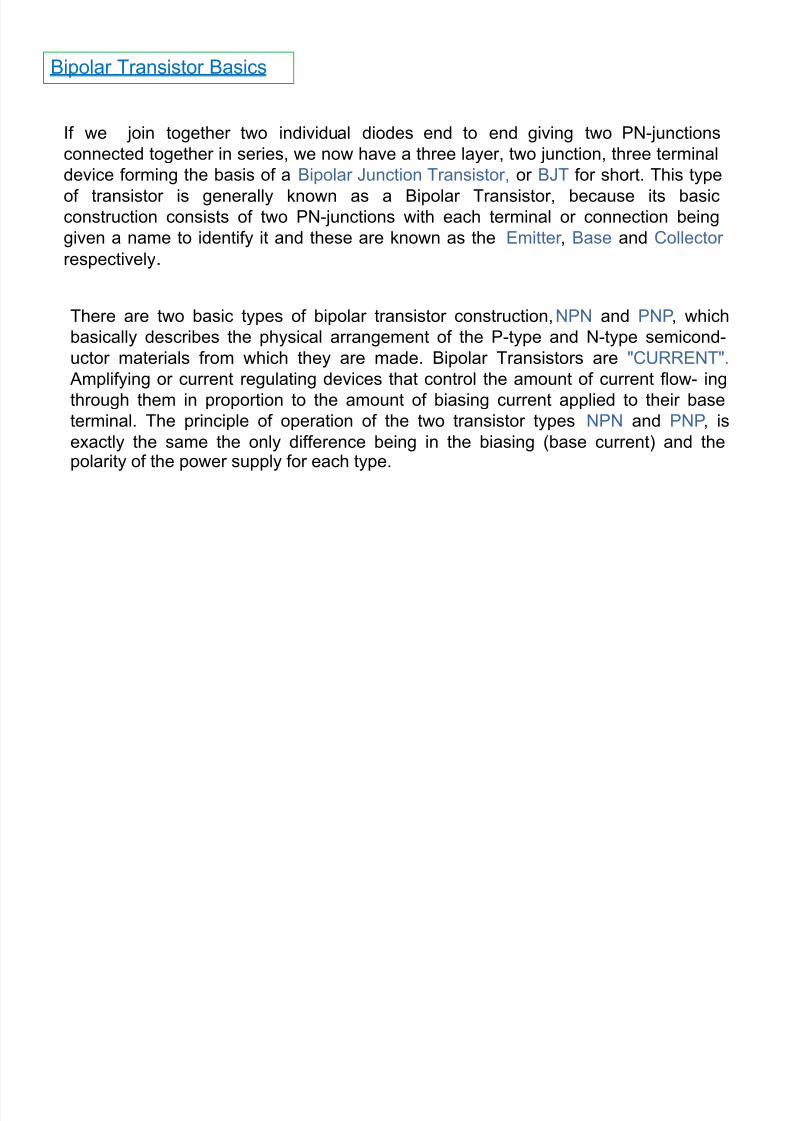
Bipolar Transistor Basics
If we join together two individual diodes end to end giving two PN-junctionsconnected together in series, we now have a three layer, two junction, three terminaldevice forming the basis of a Bipolar Junction Transistor, or BJT for short. This typeof transistor is generally known as a Bipolar Transistor, because its basicconstruction consists of two PN-junctions with each terminal or connection beinggiven a name to identify it and these are known as the Emitter , Base and Collector respectively .
There are two basic types of bipolar transistor construction, NPN and PNP , whichbasically describes the physical arrangement of the P-type and N-type semicond-uctor materials from which they are made. Bipolar Transistors are "CURRENT".
Amplifying or current regulating devices that control the amount of current flow- ingthrough them in proportion to the amount of biasing current applied to their baseterminal. The principle of operation of the two transistor types NPN and PNP , isexactly the same the only difference being in the biasing (base current) and thepolarity of the power supply for each type.

8/9/2019 BJT.touhid
http://slidepdf.com/reader/full/bjttouhid 6/38
Bipolar Transistor Construction:
FIG:01

8/9/2019 BJT.touhid
http://slidepdf.com/reader/full/bjttouhid 7/38
Transistor action
The emitter-base junction of a transistor is forward biased whereas collector-base
junction is reverse biased . If for a moment, we ignore the presence of emitter-baseJunction , then no current would flow in the collector circuit because of the reversebias. However, if the emitter-base junction is also present , then forward bias on it
causes the emitter current to flow and the emitter current almost entirely flows inthe collector circuit. Therefore , the current in the collector circuit depends upon theemitter current . If the emitter current is zero, then collector is nearly zero.
The transistor action of NPN and PNP are given below,
(i) Working of NPN transistor:
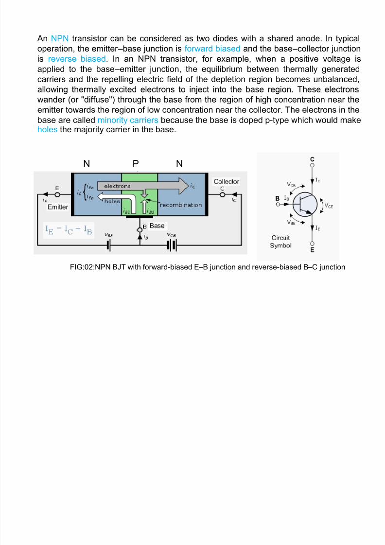
FIG:02:NPN BJT with forward-biased E –B junction and reverse-biased B – C junction
N P N
8/9/2019 BJT.touhid
http://slidepdf.com/reader/full/bjttouhid 8/38
An NPN transistor can be considered as two diodes with a shared anode. In typicaloperation, the emitter – base junction is forward biased and the base – collector junctionis reverse biased . In an NPN transistor, for example, when a positive voltage isapplied to the base – emitter junction, the equilibrium between thermally generatedcarriers and the repelling electric field of the depletion region becomes unbalanced,allowing thermally excited electrons to inject into the base region. These electronswander (or "diffuse") through the base from the region of high concentration near theemitter towards the region of low concentration near the collector. The electrons in thebase are called minority carriers because the base is doped p-type which would makeholes the majority carrier in the base.
N P N
FIG:02:NPN BJT with forward-biased E – B junction and reverse-biased B –C junction

8/9/2019 BJT.touhid
http://slidepdf.com/reader/full/bjttouhid 9/38
We know that the transistor is a "CURRENT" operated device and that a large current (Ic)flows freely through the device between the collector and the emitter terminals. However,this only happens when a small biasing current (Ib) is flowing into the base terminal of thetransistor thus allowing the base to act as a sort of current control input. The ratio of thesetwo currents (Ic/Ib) is called the DC Current Gain of the device and is given the symbol of hfe or nowadays Beta, (β) . Beta has no units as it is a ratio. Also, the current gain from theemitter to the collector terminal, Ic/Ie, is called Alpha, (α),and is a function of the transistor itself. As the emitter current Ie is the product of a very small base current to a very largecollector current the value of this parameter α is very close to unity, and for a typical low-power signal transistor this value ranges from about 0.950 to 0.999.
α and β Relationships:

8/9/2019 BJT.touhid
http://slidepdf.com/reader/full/bjttouhid 10/38
The PNP transistor works essentially the same as the NPN transistor. However, since theemitter, base, and collector in the PNP transistor are made of materials that are differentfrom those used in the NPN transistor, different current carriers
(ii) Working of PNP transistor:
By combining the two parameters α and β we can produce two mathematical expressionsthat gives the relationship between the different currents flowing in the transistor.
FIG:03:NPN BJT with forward-biased E –B junction and reverse-biased B – C junction
8/9/2019 BJT.touhid
http://slidepdf.com/reader/full/bjttouhid 11/38
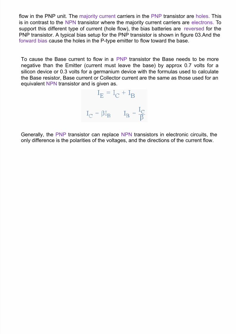
flow in the PNP unit. The majority current carriers in the PNP transistor are holes. Thisis in contrast to the NPN transistor where the majority current carriers are electrons. Tosupport this different type of current (hole flow), the bias batteries are reversed for thePNP transistor. A typical bias setup for the PNP transistor is shown in figure 03.And the
forward bias cause the holes in the P-type emitter to flow toward the base.
To cause the Base current to flow in a PNP transistor the Base needs to be morenegative than the Emitter (current must leave the base) by approx 0.7 volts for asilicon device or 0.3 volts for a germanium device with the formulas used to calculatethe Base resistor, Base current or Collector current are the same as those used for anequivalent NPN transistor and is given as.
Generally, the PNP transistor can replace NPN transistors in electronic circuits, theonly difference is the polarities of the voltages, and the directions of the current flow.
8/9/2019 BJT.touhid
http://slidepdf.com/reader/full/bjttouhid 12/38
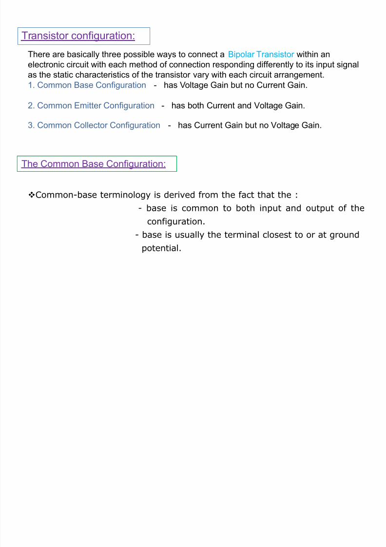
There are basically three possible ways to connect a Bipolar Transistor within an
electronic circuit with each method of connection responding differently to its input signalas the static characteristics of the transistor vary with each circuit arrangement.1. Common Base Configuration - has Voltage Gain but no Current Gain.
2. Common Emitter Configuration - has both Current and Voltage Gain.
3. Common Collector Configuration - has Current Gain but no Voltage Gain.
Transistor configuration:
The Common Base Configuration:
Common-base terminology is derived from the fact that the :- base is common to both input and output of the
configuration.- base is usually the terminal closest to or at ground
potential.
8/9/2019 BJT.touhid
http://slidepdf.com/reader/full/bjttouhid 13/38
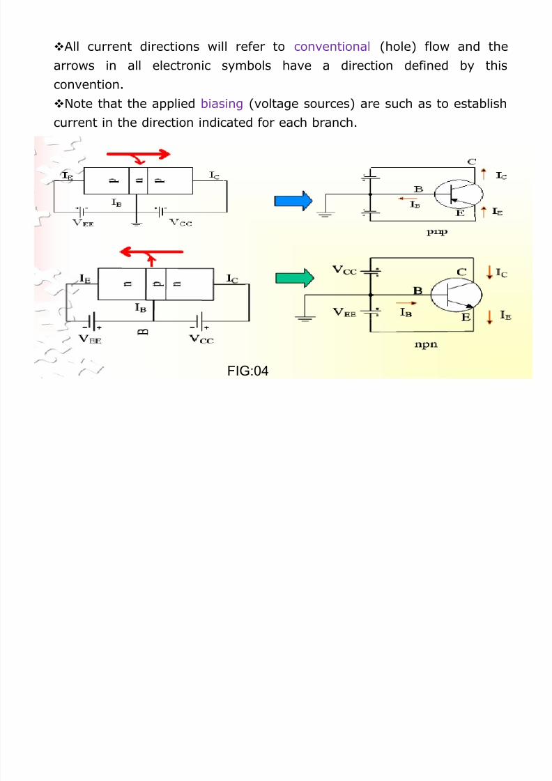
All current directions will refer to conventional (hole) flow and thearrows in all electronic symbols have a direction defined by thisconvention.
Note that the applied biasing (voltage sources) are such as to establishcurrent in the direction indicated for each branch.
FIG:04
8/9/2019 BJT.touhid
http://slidepdf.com/reader/full/bjttouhid 14/38
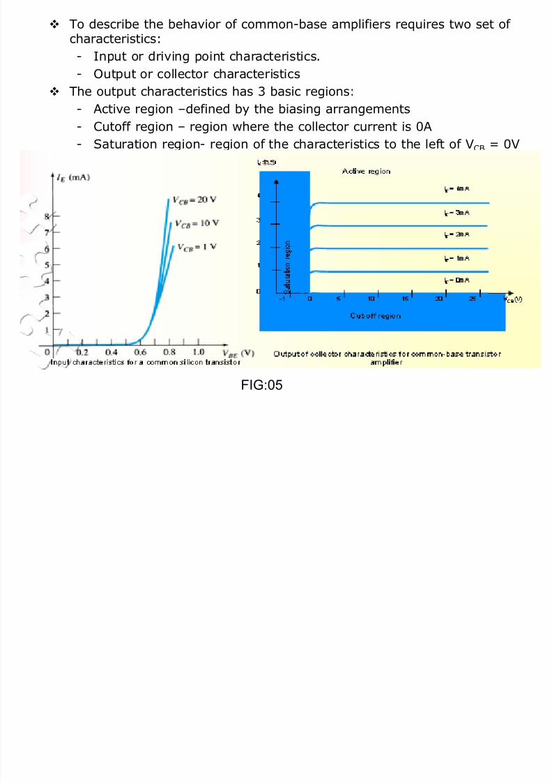
To describe the behavior of common-base amplifiers requires two set of characteristics:
- Input or driving point characteristics.- Output or collector characteristics
The output characteristics has 3 basic regions:- Active region – defined by the biasing arrangements- Cutoff region – region where the collector current is 0A- Saturation region- region of the characteristics to the left of V CB = 0V
FIG:05

8/9/2019 BJT.touhid
http://slidepdf.com/reader/full/bjttouhid 15/38
The curves (output characteristics) clearly indicate that a firstapproximation to the relationship between IE and IC in the active regionis given by
IC ≈IE Once a transistor is in the ‘on’ state, the base-emitter voltage will beassumed to be
VBE = 0.7V
8/9/2019 BJT.touhid
http://slidepdf.com/reader/full/bjttouhid 16/38
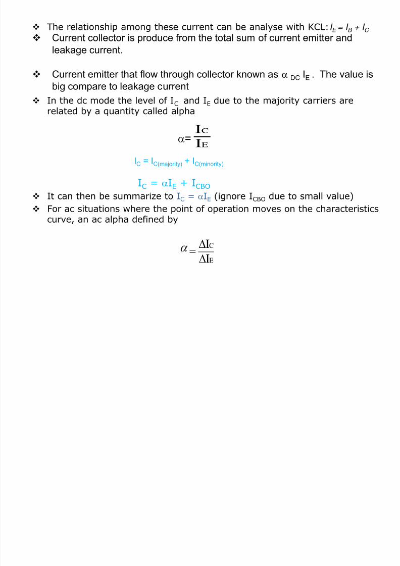
The relationship among these current can be analyse with KCL: I E = I B + I C
Current collector is produce from the total sum of current emitter andleakage current.
Current emitter that flow through collector known as DC IE . The value isbig compare to leakage current
In the dc mode the level of I C and I E due to the majority carriers arerelated by a quantity called alpha
=IC = IC(majority) + IC(minority)
IC = IE + I CBO
It can then be summarize to IC = IE (ignore I CBO due to small value)
For ac situations where the point of operation moves on the characteristicscurve, an ac alpha defined by
E
C
I
I
E
C
I
I

8/9/2019 BJT.touhid
http://slidepdf.com/reader/full/bjttouhid 17/38
Alpha a common base current gain factor that shows the efficiency bycalculating the current percent from current flow from emitter tocollector.The value of is typical from 0.9 ~ 0.998
Proper biasing CB configuration in active region by approximation I C IE (I B 0 uA)
FIG:06

8/9/2019 BJT.touhid
http://slidepdf.com/reader/full/bjttouhid 18/38
Common-Emitter ConfigurationIt is called common-emitter configuration since :
- emitter is common or reference to both input andoutput terminals.
- emitter is usually the terminal closest to or at groundpotential.
Almost ampli fier design is using connection of CE due to the high gain forcurrent and voltage.
Two set of characteristics are necessary to describe the behavior for CE;input (base terminal) and output (collector terminal) parameters.
8/9/2019 BJT.touhid
http://slidepdf.com/reader/full/bjttouhid 19/38
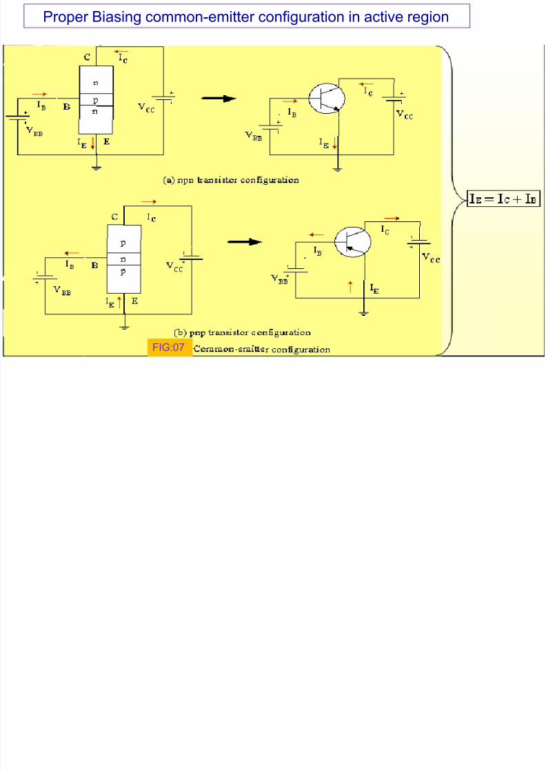
Proper Biasing common-emitter configuration in active region
FIG:07

8/9/2019 BJT.touhid
http://slidepdf.com/reader/full/bjttouhid 20/38
8/9/2019 BJT.touhid
http://slidepdf.com/reader/full/bjttouhid 21/38
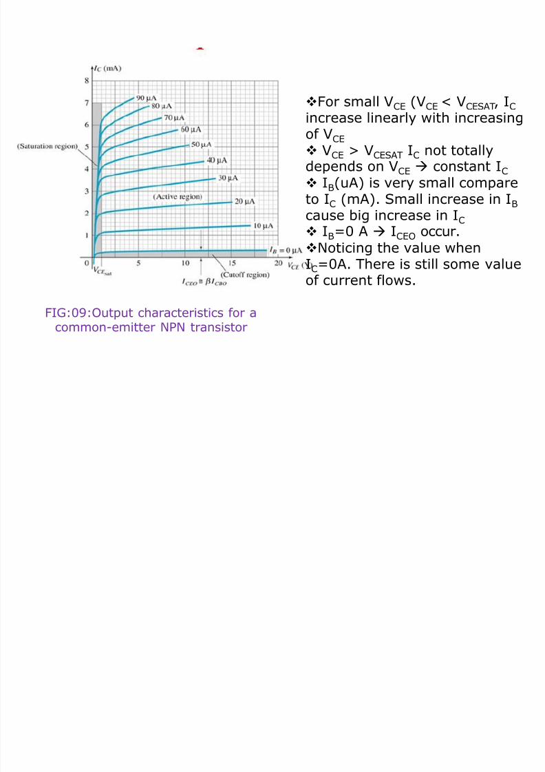
For small V CE (V CE < V CESAT , I C increase linearly with increasingof V CE
VCE > V CESAT IC not totallydepends on V CE constant I C
IB(uA) is very small compare
to I C (mA). Small increase in I B cause big increase in I C
IB=0 A ICEO occur.Noticing the value when
IC=0A. There is still some value
of current flows.FIG:09:Output characteristics for a
common-emitter NPN transistor

8/9/2019 BJT.touhid
http://slidepdf.com/reader/full/bjttouhid 22/38

8/9/2019 BJT.touhid
http://slidepdf.com/reader/full/bjttouhid 23/38
Common – Collector Configuration • Also called emitter-follower (EF).
• It is called common-emitter configuration since both the
signal source and the load share the collector terminal as acommon connection point.
• The output voltage is obtained at emitter terminal.
• The input characteristic of common-collector configuration issimilar with common-emitter. configuration.
• Common-collector circuit configuration is provided with theload resistor connected from emitter to ground.
• It is used primarily for impedance-matching purpose since ithas high input impedance and low output impedance.
8/9/2019 BJT.touhid
http://slidepdf.com/reader/full/bjttouhid 24/38
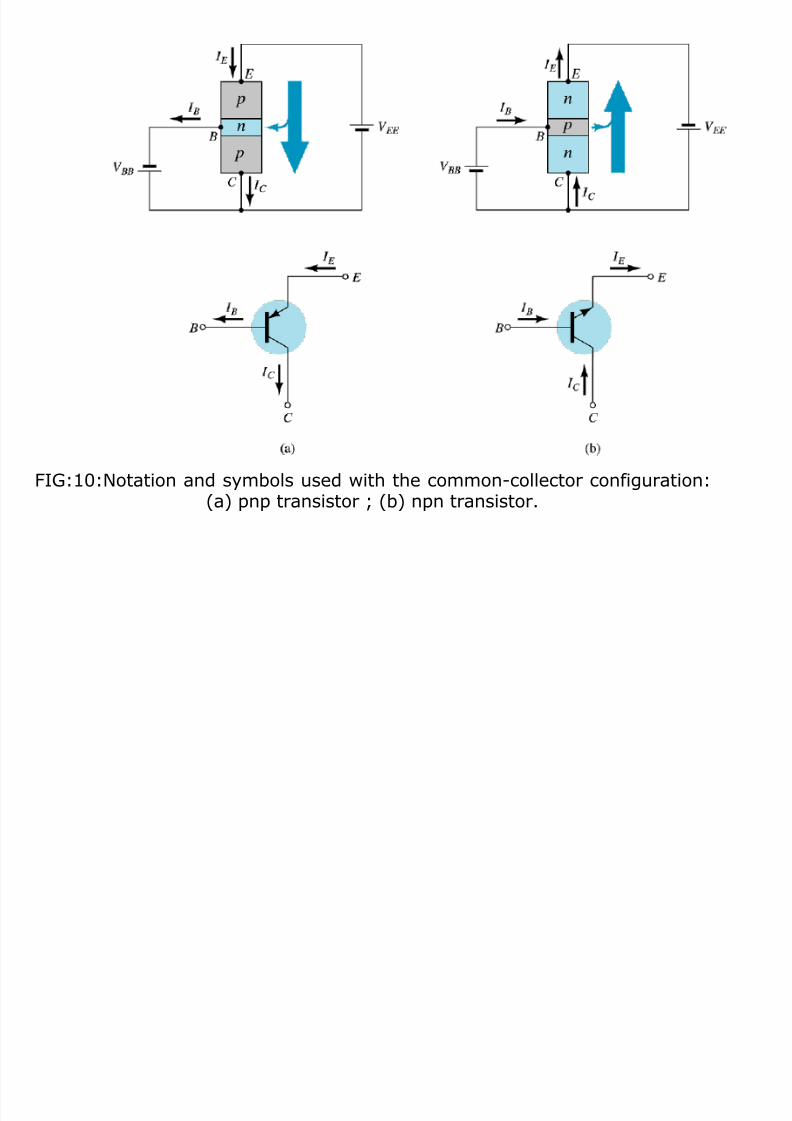
FIG:10:Notation and symbols used with the common-collector configuration:(a) pnp transistor ; (b) npn transistor.

8/9/2019 BJT.touhid
http://slidepdf.com/reader/full/bjttouhid 25/38
5
6
4
3
2
1
Saturationregion
Active region
Cutoff region
IE(mA)
V CE (V)
I B =60 uA
5 10 15V CE(sat)
IB =50 uA
IB=0 uA
IB
=40 uA
IB=30 uA
IB =20 uA
IB =10 uA
20
Fig 4.9 : Output characteristic in CC configurat ionfor npn transistor
•For the common-collector configuration, the output characteristicsare a plot of I E vs V CE for a range of values of I B.
FIG:11:
8/9/2019 BJT.touhid
http://slidepdf.com/reader/full/bjttouhid 26/38
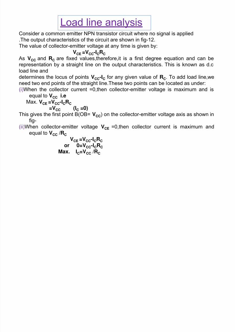
Load line analysis Consider a common emitter NPN transistor circuit where no signal is applied
.The output characteristics of the circuit are shown in fig-12.The value of collector-emitter voltage at any time is given by:VCE =VCC -ICRC
As VCC and RC are fixed values,therefore,it is a first degree equation and can berepresentation by a straight line on the output characteristics. This is known as d.cload line anddetermines the locus of points VCC -IC for any given value of RC. To add load line,we
need two end points of the straight line.These two points can be located as under:(i)When the collector current =0,then collector-emitter voltage is maximum and is
equal to VCC i.e Max. VCE =VCC -ICRC
=VCC (IC =0) This gives the first point B(OB= VCC ) on the collector-emitter voltage axis as shown in
fig-(ii)When collector-emitter voltage VCE =0,then collector current is maximum and
equal to VCC /R CVCE =VCC -ICRC
or 0=V CC -ICRCMax. I C=VCC /R C

8/9/2019 BJT.touhid
http://slidepdf.com/reader/full/bjttouhid 27/38
This gives the second point A(OA= VCC /R C) on the collector current axis asshown in fig-12
(iii) By joining these two point,d.c load line AB is constructed
A
B
FIG.12:load line analysis
RC

8/9/2019 BJT.touhid
http://slidepdf.com/reader/full/bjttouhid 28/38
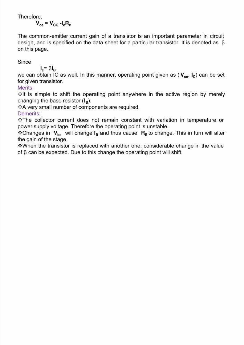
Fixed bias (base bias)
This form of biasing is also called base bias. In the example image on the right, the singlepower source (for example, a battery) is used for both collector and base of transistor,although separate batteries can also be used.
In the given circuit,
VCC = IBRB+ Vbe
Therefore,
IB= ( VCC - Vbe )/RB
For a given transistor, Vbe does not vary significantly during use. As VCC is of fixed value,on selection of RB, the base current IB is fixed. Therefore this type is called fixed bias typeof circuit.
Also for given circuit,
VCC = ICRC+ Vce
FIG:13:Fixed bias (Base bias)
8/9/2019 BJT.touhid
http://slidepdf.com/reader/full/bjttouhid 29/38
Therefore,Vce = VCC -IcR c
The common-emitter current gain of a transistor is an important parameter in circuit
design, and is specified on the data sheet for a particular transistor. It is denoted as β on this page.
SinceIc= β IB
we can obtain IC as well. In this manner, operating point given as ( Vce , IC) can be setfor given transistor.Merits:
It is simple to shift the operating point anywhere in the active region by merelychanging the base resistor ( IB).
A very small number of components are required.Demerits:
The collector current does not remain constant with variation in temperature or
power supply voltage. Therefore the operating point is unstable.Changes in Vbe will change IB and thus cause RE to change. This in turn will alter the gain of the stage.
When the transistor is replaced with another one, considerable change in the valueof β can be expected. Due to this change the operating point will shift.

8/9/2019 BJT.touhid
http://slidepdf.com/reader/full/bjttouhid 30/38
This configuration employs negative feedback to
prevent thermal runaway and stabilize the operatingpoint. In this form of biasing, the base resistor RB isconnected to the collector instead of connecting it tothe DC source VCC . So any thermal runaway willinduce a voltage drop across the RC resistor that willthrottle the transistor's base current.From Kirchhoff's voltage law, the voltage acrossthe base resistor is RB.
Collector-to-base bias
FIG:14:Collector-to-base bias
here, Ic= βI
B
From Ohm's law, the base current , and so

8/9/2019 BJT.touhid
http://slidepdf.com/reader/full/bjttouhid 31/38
hence, the base current Ib is,
If Vbe is held constant and temperature increases, then the collector currentIc increases. However, a larger Ic causes the voltage drop across resistor R c to increase, which in turn reduces the voltage across the base resistor Rb . A lower base-resistor voltage drop reduces the base current Ib , whichresults in less collector current Ib . Because an increase in collector current
with temperature is opposed, the operating point is kept stable.
Merits:Circuit stabilizes the operating point against variations in temperature and β
(ie. replacement of transistor).
Demerits:In this circuit, to keep Ic independent of β, the following condition must be
met:
.

8/9/2019 BJT.touhid
http://slidepdf.com/reader/full/bjttouhid 32/38
which is the case when
As β-value is fixed (and generally unknown) for a given transistor, this relation canbe satisfied either by keeping Rc fairly large or making Rb very low.
If R c is large, a high Vcc is necessary, which increases cost as well as precautionsnecessary while handling.
If Rb is low, the reverse bias of the collector-base is small, which limits the range of collector voltage swing that leaves the transistor in active mode.
The resistor Rb causes an AC feedback, reducing the voltage gain of the amplifier.This undesirable effect is a trade-off for greater Q-point stability
Usage:
Due to the above inherent drawbacks, fixed bias is rarely used in linear circuits, ie.those circuits which use the transistor as a current source. Instead it is often used incircuits where transistor is used as a switch.
8/9/2019 BJT.touhid
http://slidepdf.com/reader/full/bjttouhid 33/38
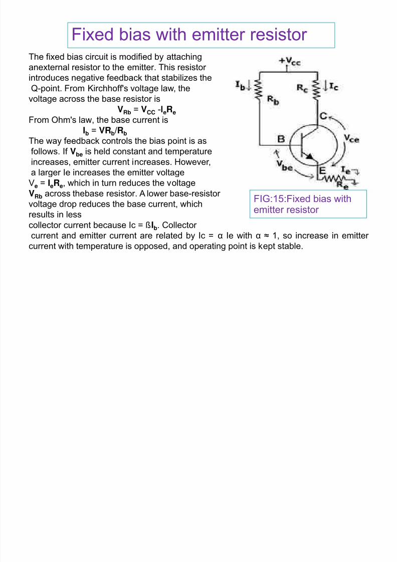
Fixed bias with emitter resistor The fixed bias circuit is modified by attaching
anexternal resistor to the emitter. This resistor introduces negative feedback that stabilizes theQ-point. From Kirchhoff's voltage law, the
voltage across the base resistor isVRb = VCC -IeR e
From Ohm's law, the base current is Ib = VRb /Rb
The way feedback controls the bias point is asfollows. If Vbe is held constant and temperatureincreases, emitter current increases. However,a larger Ie increases the emitter voltage
Ve = IeR e , which in turn reduces the voltageVRb across thebase resistor. A lower base-resistor voltage drop reduces the base current, whichresults in lesscollector current because Ic = ß Ib . Collector current and emitter current are related by Ic = α Ie with α ≈ 1, so increase in emitter
current with temperature is opposed, and operating point is kept stable.
FIG:15:Fixed bias with
emitter resistor
8/9/2019 BJT.touhid
http://slidepdf.com/reader/full/bjttouhid 34/38
Similarly, if the transistor is replaced by another, there may be a change in IC(corresponding to change in β-value, for example). By similar process as above, thechange is negated and operating point kept stable.For the given circuit,
IB= (V CC - Vbe )/(Rb + (β+ 1)RE Merits:
The circuit has the tendency to stabilize operating point against changes intemperature and β -value.Demerits:
In this circuit, to keep IC independent of β the following condition must be met:
which is approximately the case if ( β + 1 ) RB >> RB.
As β -value is fixed for a given transistor, this relation can be satisfied either bykeeping RE very large, or making RB very low.If RE is of large value, high V
CCis necessary. This increases cost as well as
precautions necessary while handling.If RB is low, a separate low voltage supply should be used in the base circuit. Usingtwo supplies of different voltages is impractical.In addition to the above, RE causes ac feedback which reduces the voltage gain of the amplifier.
8/9/2019 BJT.touhid
http://slidepdf.com/reader/full/bjttouhid 35/38
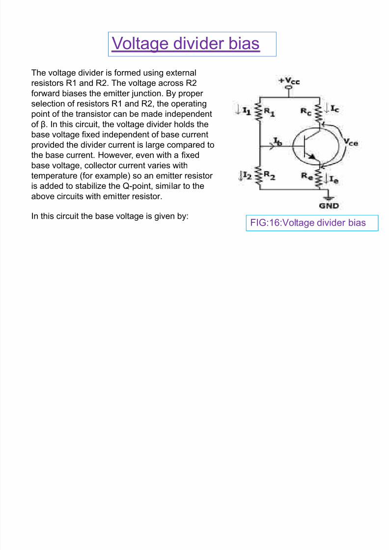
Voltage divider bias
The voltage divider is formed using externalresistors R1 and R2. The voltage across R2forward biases the emitter junction. By proper selection of resistors R1 and R2, the operatingpoint of the transistor can be made independentof β. In this circuit, the voltage divider holds the
base voltage fixed independent of base currentprovided the divider current is large compared tothe base current. However, even with a fixedbase voltage, collector current varies withtemperature (for example) so an emitter resistor is added to stabilize the Q-point, similar to theabove circuits with emitter resistor.
In this circuit the base voltage is given by: FIG:16:Voltage divider bias

8/9/2019 BJT.touhid
http://slidepdf.com/reader/full/bjttouhid 36/38
voltage across
provided
Also
For the given circuit ,
Merits:
Unlike above circuits, only one dc supply is necessary.Operating point is almost independent of β variation. Operating point stabilized against shift in temperature.
Demerits:
In this circuit, to keep IC independent of β the following condition must be met:

8/9/2019 BJT.touhid
http://slidepdf.com/reader/full/bjttouhid 37/38
which is approximately the case if
where R1 || R2 denotes the equivalent resistance of R1 and R2 connected in parallel.
As β -value is fixed for a given transistor, this relation can be satisfied either bykeeping RE fairly large, or making R1||R2 very low.
If RE is of large value, high V CC is necessary. This increases cost as well asprecautions necessary while handling.
If R1 || R2 is low, either R1 is low, or R2 is low, or both are low. A low R1 raises V B closer to V
C, reducing the available swing in collector voltage, and limiting how large
RC can be made without driving the transistor out of active mode. A low R2 lowers Vbe,reducing the allowed collector current. Lowering both resistor values draws morecurrent from the power supply and lowers the input resistance of the amplifier as seenfrom the base.
AC as well as DC feedback is caused by RE, which reduces the AC voltage gain of the amplifier. A method to avoid AC feedback while retaining DC feedback is discussed
below.
Usage:The circuit's stability and merits as above make it widely used for linear circuits

8/9/2019 BJT.touhid
http://slidepdf.com/reader/full/bjttouhid 38/38
Emitter bias
When a split supply (dual power supply) is available, thisBiasing circuit is the most effective, and provides zerobias voltage at the emitter or collector for load. Thenegative supply V EE is used to forward-bias the emitter junction through R E. The positive supply V CC is usedto reverse-bias the collector junction. Only two resistorsare necessary for the common collector stage and four
resistors for the common emitter or common base stage.We know that,VB -VE =Vbe If RB is small enough, base voltage will be approximatelyzero. Therefore emitter current is,IE = ( VEE -Vbe )/RE. The operating point is independentof β if RE >> RB/β Merit:Good stability of operating point similar to voltage divider bias.Demerit:This type can only be used when a split (dual) power supply is available .
FIG:17:Emitter bias