BiTS 2017 March 5-8, 2017 Burn-in & Test Strategies Workshop www.bitsworkshop.org Tutorial: Interconnect Sockets and Applications Tutorial March 5 - 8, 2017 Hilton Phoenix / Mesa Hotel Mesa, Arizona © 2017 BiTS Workshop – Image: tonda / iStock

Welcome message from author
This document is posted to help you gain knowledge. Please leave a comment to let me know what you think about it! Share it to your friends and learn new things together.
Transcript

BiTS 2017
March 5-8, 2017 Burn-in & Test Strategies Workshop www.bitsworkshop.org
Tutorial: Interconnect Sockets and Applications
Archive -Tutorial
March 5 - 8, 2017
Hilton Phoenix / Mesa Hotel
Mesa, Arizona
© 2017 BiTS Workshop – Image: tonda / iStock

BiTS 2017
March 5-8, 2017 Burn-in & Test Strategies Workshop www.bitsworkshop.org
Copyright Notice
The presentation(s)/poster(s) in this publication comprise the Proceedings of the 2017 BiTS Workshop. The content reflects the opinion of the authors and their respective companies. They are reproduced here as they were presented at the 2017 BiTS Workshop. This version of the presentation or poster may differ from the version that was distributed in hardcopy & softcopy form at the 2017 BiTS Workshop. The inclusion of the presentations/posters in this publication does not constitute an endorsement by BiTS Workshop or the workshop’s sponsors. There is NO copyright protection claimed on the presentation/poster content by BiTS Workshop. However, each presentation/poster is the work of the authors and their respective companies: as such, it is strongly encouraged that any use reflect proper acknowledgement to the appropriate source. Any questions regarding the use of any materials presented should be directed to the author(s) or their companies. The BiTS logo and ‘Burn-in & Test Strategies Workshop’ are trademarks of BiTS Workshop. All rights reserved.

BiTS 2017
March 5-8, 2017 Burn-in & Test Strategies Workshop www.bitsworkshop.org
Tutorial: Interconnect Sockets and Applications
BiTS Workshop 2017 Schedule
Tutorial Day Sunday March 5 - Noon
Interconnect Sockets and Applications
In this tutorial, we will go over the socket contact element fundamentals, types of socket contact elements, contact element
materials, and printed circuit board (PCB) & hardware requirements. We will also cover electrical, and system design and test requirements.
We will provide you with different options for selecting interconnect sockets depending on your requirements like signal integrity, cycle life,
cost, etc.
Ashok Kabadi - AK Technology Leadership
Mohan Prabhugoud - Intel
Tutorial

BiTS 2017
March 5-8, 2017 Burn-in & Test Strategies Workshop www.bitsworkshop.org
Tutorial: Interconnect Sockets and Applications
Tutorial – Abstract
In this tutorial, we will go over the socket contact element fundamentals, types of socket contact elements, contact element materials, and printed circuit board (PCB) & hardware requirements. We will also cover electrical, and system design and test requirements. We will provide you with different options for selecting interconnect sockets depending on your requirements like signal integrity, cycle life, cost, etc. At the end of the course, you will have a clear understanding of the types of sockets available in the industry, how to select the best one for your needs, and how to successfully develop and implement the same. Target audience includes: PCB designers, mechanical engineers, hardware engineers, hardware engineering managers, and materials engineers.
Ashok Kabadi
Mohan Prabhugoud

BiTS 2017
March 5-8, 2017 Burn-in & Test Strategies Workshop www.bitsworkshop.org
Tutorial: Interconnect Sockets and Applications
Tutorial – Objectives
Objectives
• Understand what the interconnect socket is and its benefits
• Understand the contact elements and resistances
• Understand different types of interconnect sockets available in the industry and their applications
• Provide overview of different PCB plating available in the industry and their applications
• Understand mechanical system design methodologies with special emphasis on tolerances, PCB Keep-Out-Zones (KOZs) and retention design
• Provide overview of electrical signal integrity measurements
• Understand test and validation requirements for interconnect technologies
• Understand the entire end-to-end process flow, right from gathering the requirements to successful implementation
Ashok Kabadi
Mohan Prabhugoud

BiTS 2017
March 5-8, 2017 Burn-in & Test Strategies Workshop www.bitsworkshop.org
Tutorial: Interconnect Sockets and Applications
Tutorial – Biography Ashok Kabadi joined Intel as a Manufacturing Engineer in the Systems Manufacturing Department in 1981. Over his thirty-five year career at Intel, his technological innovations advanced the high-tech industry. His last role was Mechanical Architect and Senior Principal Engineer in the Platform Hardware Group (PHG). Ashok drove the development of multiple advanced platform technologies whichhad significant and measurable impact on improving the cost and time-to-market (TTM) of Intel products as well as external customer products, These technologies included Metallized Particle Interconnect (MPI) sockets, zero keepout (ZKO) sockets, and coax via technology. Ashok was also the key driver for building the Technical Leadership Program in Guadalajara, Mexico (GDC), as well as personally mentoring and growing the pipeline of technical talent in GDC.
He has a deep passion for innovation in the areas of socket interconnect, thermal design, and printed circuit boards. In addition to 16 patents, he has delivered multiple publications, presentations and talks at conferences within the US and internationally. Ashok is now Managing Director of AK Technology (AKT) Leadership providing consulting services and the BiTS Workshop Technical Program Co-chair.
Mohanraj Prabhugoud is currently a Senior Mechanical Engineer at Intel Corporation. He has worked on mechanical design of sockets, socket retention, thermal margining tool, heat sink, PCBs, chassis, etc. for over ten years. Mohan received his MS and PhD in Mechanical Engineering degrees from North Carolina State University.
Ashok Kabadi
Mohan Prabhugoud

Tutorial: Interconnect Sockets and ApplicationsBiTS 2017
March 5-8, 2017Burn-in & Test Strategies Workshop www.bitsworkshop.org
Interconnect Sockets and
Applications
Ashok Kabadi – AK Technology Leadership
Mohan Prabhugoud – Intel Corp.
BiTS Workshop
March 5 - 8, 2017Conference Ready
mm/dd/2014

Tutorial: Interconnect Sockets and ApplicationsBiTS 2017
March 5-8, 2017Burn-in & Test Strategies Workshop www.bitsworkshop.org
Agenda
1. Introduction and Background
– Second-Level-Interconnect definition
– Purpose of sockets
– Benefits of sockets
2. Contact Element
– Single-compression Vs Dual-compression
– Contact resistance theory
– Examples of calculating resistances
– Relationship between Contact load, Contact travel and Contact
resistance
Interconnect Sockets and Applications 2

Tutorial: Interconnect Sockets and ApplicationsBiTS 2017
March 5-8, 2017Burn-in & Test Strategies Workshop www.bitsworkshop.org
Agenda
3. Types of Contacts
– Polymer –based
• Metallized and wire-type
– Particle Interconnect
– Metal-based
• MEMS–based
• Spring–loaded
• Stamped-and-formed
• Screw-machine
• Buckling
– Summary
Break --- 30 minutes
Interconnect Sockets and Applications 3

Tutorial: Interconnect Sockets and ApplicationsBiTS 2017
March 5-8, 2017Burn-in & Test Strategies Workshop www.bitsworkshop.org
Agenda
4. Contact Element Material
– Contact material requirement
– Types of material and plating
– Contact material selection
5. Printed-Circuit-Board and Hardware Requirements
– Surface finish requirement
– Mechanical tolerances (positional and absolute)
– Keep-Out Zones (KOZ)
Interconnect Sockets and Applications 4

Tutorial: Interconnect Sockets and ApplicationsBiTS 2017
March 5-8, 2017Burn-in & Test Strategies Workshop www.bitsworkshop.org
Agenda
6. Electrical Characterization: Signal-Integrity (SI)
– Insertion loss
– Cross-talk
– Current carrying capacity
– Impedance (capacitance and inductance)
Break --- 30 minutes
7. Interconnect Socket and System Design
– Types of interconnect system
– Mechanical hardware design and tolerances
– Force-Deflection analysis
Interconnect Sockets and Applications 5
Tutorial: Interconnect Sockets and ApplicationsBiTS 2017
March 5-8, 2017Burn-in & Test Strategies Workshop www.bitsworkshop.org
Agenda
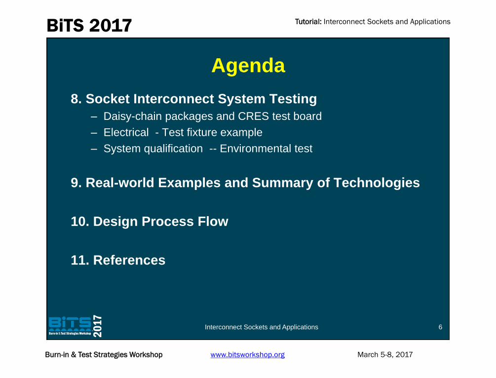
8. Socket Interconnect System Testing
– Daisy-chain packages and CRES test board
– Electrical - Test fixture example
– System qualification -- Environmental test
9. Real-world Examples and Summary of Technologies
10. Design Process Flow
11. References
Interconnect Sockets and Applications 6

Tutorial: Interconnect Sockets and ApplicationsBiTS 2017
March 5-8, 2017Burn-in & Test Strategies Workshop www.bitsworkshop.org
Section 1
Introduction and Background
7Interconnect Sockets and Applications

Tutorial: Interconnect Sockets and ApplicationsBiTS 2017
March 5-8, 2017Burn-in & Test Strategies Workshop www.bitsworkshop.org
Interconnect Socket Definition
8
An electrically conductive
interface element placed
between an electronic
component and a printed-
circuit-board to make reliable
interconnection between the
device and PCB
Printed Circuit Board (PCB)Conductive Element (Socket)
Electronic Component/device (e.g. BGA)
Interconnect Socket Schematic
Types of sockets/connectors
F
F
Interconnect Sockets and Applications

Tutorial: Interconnect Sockets and ApplicationsBiTS 2017
March 5-8, 2017Burn-in & Test Strategies Workshop www.bitsworkshop.org
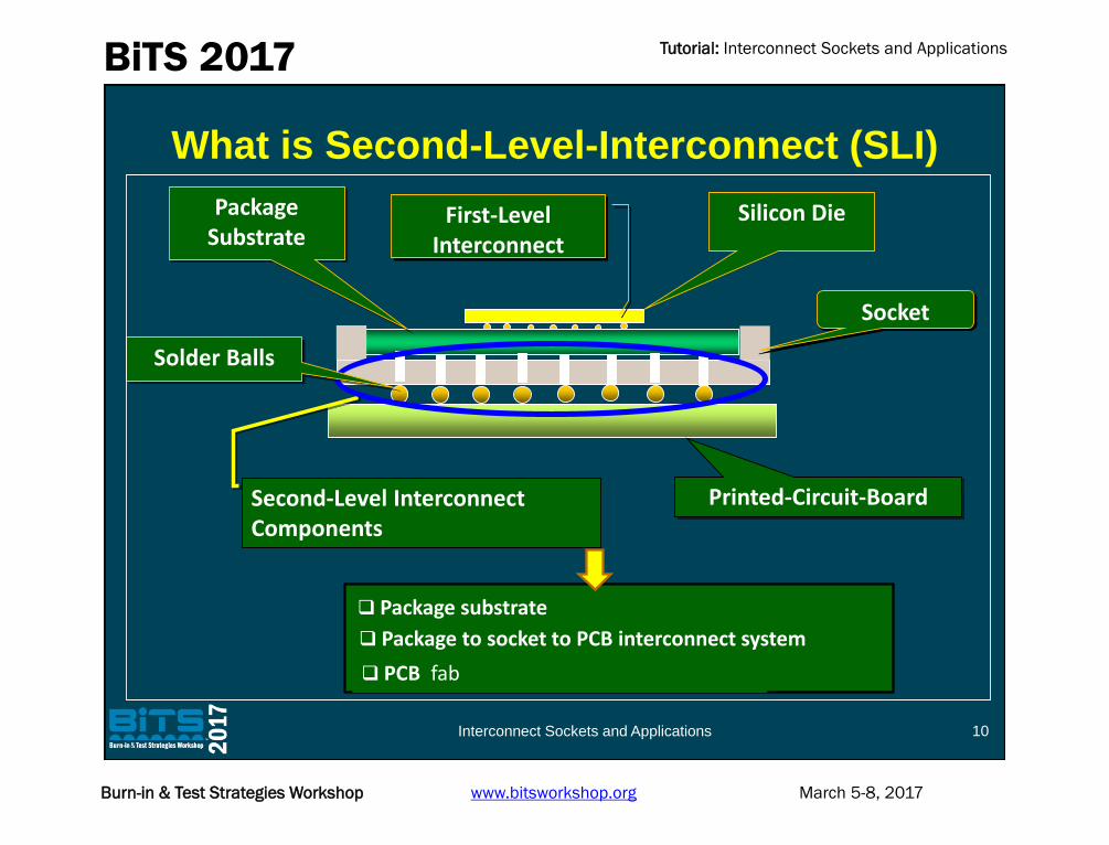
What is Second-Level-Interconnect (SLI)
9
Silicon DiePackageSubstrate
First-Level Interconnect
Second -Level Interconnect Printed-Circuit-Board
Solder Balls(Pb or Pb-free)
JEDEC Definition:
Interconnect Sockets and Applications
Tutorial: Interconnect Sockets and ApplicationsBiTS 2017
March 5-8, 2017Burn-in & Test Strategies Workshop www.bitsworkshop.org
What is Second-Level-Interconnect (SLI)
10
Silicon DiePackageSubstrate
First-Level Interconnect
Second-Level Interconnect Printed-Circuit-Board
Socket
Second-Level Interconnect Components
Package substrate
Package to socket to PCB interconnect system
PCB fab
Solder Balls
Interconnect Sockets and Applications
Tutorial: Interconnect Sockets and ApplicationsBiTS 2017
March 5-8, 2017Burn-in & Test Strategies Workshop www.bitsworkshop.org
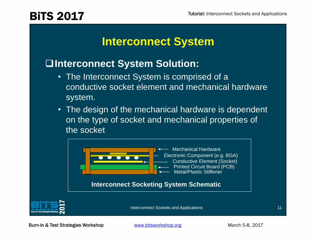
Interconnect System
Interconnect System Solution:
• The Interconnect System is comprised of a
conductive socket element and mechanical hardware
system.
• The design of the mechanical hardware is dependent
on the type of socket and mechanical properties of
the socket
11
Printed Circuit Board (PCB)Conductive Element (Socket)
Electronic Component (e.g. BGA)
Interconnect Socketing System Schematic
Mechanical Hardware
Metal/Plastic Stiffener
Interconnect Sockets and Applications

Tutorial: Interconnect Sockets and ApplicationsBiTS 2017
March 5-8, 2017Burn-in & Test Strategies Workshop www.bitsworkshop.org
Types and Benefits of Sockets
Test Sockets:
• Testing multiple devices using the same socket attached
to the same PCB -- cannot be done if the device is
soldered
• Typically low volume quantities but requires hundreds of
thousands of insertions/removal cycles for high-volume
device testing
Validation Sockets:
• Used during the first power-on of the new silicon.
Validation of multiple silicon using the same socket
attached to same PCB – Cannot be done if the device is
soldered
12Interconnect Sockets and Applications

Tutorial: Interconnect Sockets and ApplicationsBiTS 2017
March 5-8, 2017Burn-in & Test Strategies Workshop www.bitsworkshop.org
Types and Benefits of Sockets
Validation Sockets (Cont’d.)
• During subsequent silicon stepping changes
• Typically medium volume and requires medium number of
insertion/removal cycles
Production Sockets for Products
• Allows PCBs assembled ahead of silicon arrival -
Cannot be done if the device is soldered
• Low number of insertion/removal cycles but high
volume quantity
• Low cost/unit
• High tooling cost
13Interconnect Sockets and Applications

Tutorial: Interconnect Sockets and ApplicationsBiTS 2017
March 5-8, 2017Burn-in & Test Strategies Workshop www.bitsworkshop.org
Examples of Different Types of Sockets
14
Test Sockets
• Typically uses pogo-pins
Validation Sockets
• Typically uses elastomeric
contact pins
Production sockets
• Typically uses stamped-and
- formed pins
Interconnect Sockets and Applications
Tutorial: Interconnect Sockets and ApplicationsBiTS 2017
March 5-8, 2017Burn-in & Test Strategies Workshop www.bitsworkshop.org
15
Section 2
Contact Element Fundamentals
Interconnect Sockets and Applications

Tutorial: Interconnect Sockets and ApplicationsBiTS 2017
March 5-8, 2017Burn-in & Test Strategies Workshop www.bitsworkshop.org
Single-compression Socket
16
Definition:Socket is defined as a single-compression socket when
the contact element is soldered to the surface of one device
(typically of a PCB) and compressed at the other end where it
interfaces with the second device (typically a BGA component)
BGA Component
Printed-Circuit-Board
Compressed End
Soldered End
Force
Contact spring
element
Interconnect Sockets and Applications

Tutorial: Interconnect Sockets and ApplicationsBiTS 2017
March 5-8, 2017Burn-in & Test Strategies Workshop www.bitsworkshop.org
Dual-compression Socket
17
Definition:Socket is defined as a dual-compression socket when
the contact element is compressed between the two
surfaces to make electrical connection. These surfaces are
typically PCB at one end and BGA device at the other end.
BGA Component
Printed-Circuit-Board
Compressed one end
Compressed other end
Force
Force
Pad typically plated with Nickel
and Gold
Contact spring
element
Interconnect Sockets and Applications

Tutorial: Interconnect Sockets and ApplicationsBiTS 2017
March 5-8, 2017Burn-in & Test Strategies Workshop www.bitsworkshop.org
Contact Resistance Theory
Contact resistance occurs between
Interconnect pin surface and PCB pad surface
Interconnect pin surface and solder ball surface
Higher contact resistance results in thermal and electrical
losses
Practical surfaces have surface roughness due to
manufacturing operations
Practical Contact Area << Design Contact Area
18
Surface1
Surface2
Practical
contact area
Force
Force
Surface
Design contact area
Interconnect Sockets and Applications

Tutorial: Interconnect Sockets and ApplicationsBiTS 2017
March 5-8, 2017Burn-in & Test Strategies Workshop www.bitsworkshop.org
Contact Resistance Theory (Cont’d.)
Thin film forms on metal surfaces (Cu, W, Ag, etc) due to
oxidation
Interconnect pin wiping action is used to break oxide film
lowering contact resistance
Interconnect pin punctures into oxide film lowering
contact resistance for vertical interconnect pins
19
Metal
Oxide film
Solder ball
Interconnect
pin
Crown tip
Interconnect Sockets and Applications

Tutorial: Interconnect Sockets and ApplicationsBiTS 2017
March 5-8, 2017Burn-in & Test Strategies Workshop www.bitsworkshop.org
Contact Resistance Theory (Cont’d.)
Total Contact Resistance = Ri-ball + Ri + Ri-pad
• Ri-ball: Contact resistance between interconnect and ball
• Ri: Bulk resistance of interconnect
• Ri-pad: Contact resistance between interconnect and PCB
pad
20
Ri-ball
Ri-pad
Ri
PCB
BGA DeviceSolder-ball
Cu pad
Contact Spring
element
Ri-ball
Ri
Ri-pad
Interconnect Sockets and Applications

Tutorial: Interconnect Sockets and ApplicationsBiTS 2017
March 5-8, 2017Burn-in & Test Strategies Workshop www.bitsworkshop.org
Contact Resistance Theory: Bulk
Resistance
Bulk Resistance Ri =ρ𝐿
𝐴
• ρ: Resistivity of the interconnect material (Ω-m)
• L: Length of the interconnect (m)
• A: Cross-sectional area of interconnect (m2)
21
MaterialResistivity(Ω-m)
at 20oC
Bulk Resistance
(mΩ) at 20oC
Copper 1.68x10⁻⁸ 2.05
Silver 1.59x10⁻⁸ 1.94
Gold 2.44x10⁻⁸ 2.98
Tungsten 5.6x10⁻⁸ 6.84
Stainless Steel 69x10-8 84.34
Length of interconnect: 6mm
Diameter of interconnect:
0.25mm
Assumption:
Interconnect Sockets and Applications

Tutorial: Interconnect Sockets and ApplicationsBiTS 2017
March 5-8, 2017Burn-in & Test Strategies Workshop www.bitsworkshop.org
Contact Resistance: Relationship with
Force Linear or non-linear behavior of Force/Load and Compression
relationship
• Analyzed using Finite Element Analysis and experimentally validated
Total Resistance and Force/Load relationship is experimentally
measured
22
PCB
BGA Device
Free State
Total Force F=0
Fixed Boundary
Compression
δ=0
Compressed State
PCB
BGA Device
Total Force F
Fixed Boundary
Compression δ
Interconnect Sockets and Applications
Tutorial: Interconnect Sockets and ApplicationsBiTS 2017
March 5-8, 2017Burn-in & Test Strategies Workshop www.bitsworkshop.org
Contact Resistance: Relationship with
Force (Cont’d.)
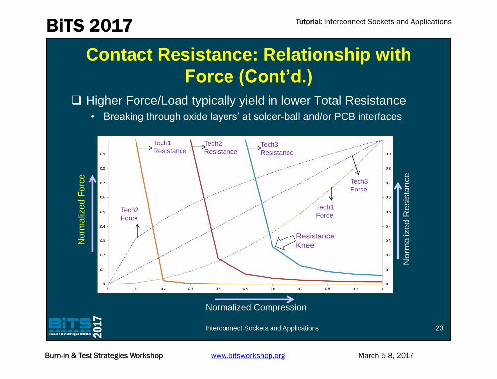
Higher Force/Load typically yield in lower Total Resistance
• Breaking through oxide layers’ at solder-ball and/or PCB interfaces
23
No
rma
lized F
orc
e
No
rma
lize
d R
esis
tan
ce
Normalized Compression
Tech1
ResistanceTech2
ResistanceTech3
Resistance
Tech1
ForceTech2
Force
Tech3
Force
Resistance
Knee
Interconnect Sockets and Applications

Tutorial: Interconnect Sockets and ApplicationsBiTS 2017
March 5-8, 2017Burn-in & Test Strategies Workshop www.bitsworkshop.org
Contact Resistance: Relationship with
Force (Cont’d.) Normal Force and Compression can be non-linear
relationship
24
No
rma
lized F
orc
e
No
rma
lized R
esis
tan
ce
Normalized Compression
Tech1
ResistanceTech2
ResistanceTech3
Resistance
Tech1
Force
Tech2
Force
Tech3
Force
Interconnect Sockets and Applications

Tutorial: Interconnect Sockets and ApplicationsBiTS 2017
March 5-8, 2017Burn-in & Test Strategies Workshop www.bitsworkshop.org
Contact Element Characterization
Important to characterize contact element performance
prior to building an array/socket
• Typically performed by building a small coupon with 1-4
contact elements
Mechanical characterization includes
• Force Vs Compression at room & at high temperature (>100ºC)
• Maximum force/compression to yield/set
• Number of cycles to failure (material yielding, tip plating wear, etc)
Electrical characteristics include
• Total resistance of contact element at room and at high
temperature (>100ºC)
• Current carrying capability at room and at high temperature
(>100ºC)
25Interconnect Sockets and Applications
Tutorial: Interconnect Sockets and ApplicationsBiTS 2017
March 5-8, 2017Burn-in & Test Strategies Workshop www.bitsworkshop.org
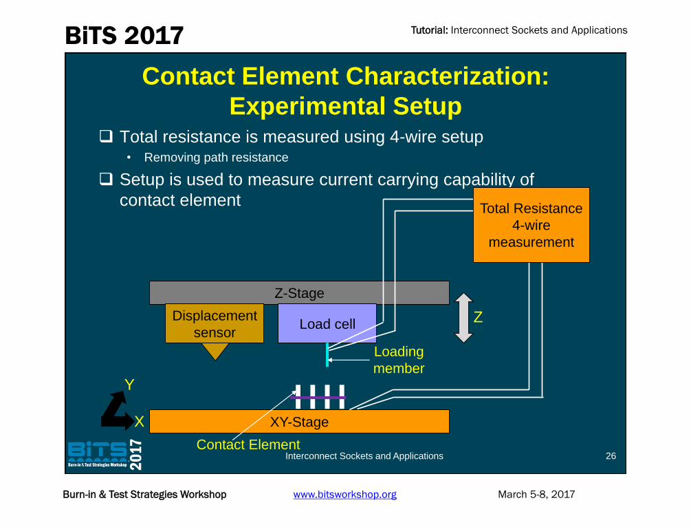
Contact Element Characterization:
Experimental Setup Total resistance is measured using 4-wire setup
• Removing path resistance
Setup is used to measure current carrying capability of
contact element
26
XY-Stage
Z-Stage
Displacement
sensorLoad cell Z
X
Y
Loading
member
Total Resistance
4-wire
measurement
Contact ElementInterconnect Sockets and Applications
Tutorial: Interconnect Sockets and ApplicationsBiTS 2017
March 5-8, 2017Burn-in & Test Strategies Workshop www.bitsworkshop.org
27
Section 3
Types of Contacts
Interconnect Sockets and Applications

Tutorial: Interconnect Sockets and ApplicationsBiTS 2017
March 5-8, 2017Burn-in & Test Strategies Workshop www.bitsworkshop.org
Polymer-based Contacts
28
Primary Advantages:• No ball damage
• Easily replaced as needed
• Custom and mixed pitch
• Excellent electrical characteristics
• Can be scaled down to <0.4mm
Two types of Contacts:1. Polymer filled with metal powder
2. Polymer with embedded metal spring element
1. Polymer filled with conductive metal powder
Courtesy: ISC
Polymer
Metal powder
(Ag or Au)
BGA Device
Interconnect Sockets and Applications

Tutorial: Interconnect Sockets and ApplicationsBiTS 2017
March 5-8, 2017Burn-in & Test Strategies Workshop www.bitsworkshop.org
Polymer-based Contacts (Cont’d.)
29
Shin-poly technology
A Matrix of vertical wires suspended in
a non conductive polymer.
Suspended in 2 configurations, GB
(vertical wires) and MT (angled wires).
Both with wire pitches as small as .03
mm. (approx. 1mil)
MT Matrix
Schematic of stack-up
Package
PCB
BGA Package
pitch 0.65mm0.31mm
Wire pitch 0.1mm
Au plated Brass wire diameter 0.04mm
BGA Package pitch 0.65mm
Wire pitch 0.1mm
compression of polymer showing number of wires
connecting per BGA
Primary Advantages:• Extremely Low Height
• Custom and mixed pitch
• Excellent electrical characteristics
• Can be scaled down to <0.4mm
1. Polymer filled with Conductive metal powder
Courtesy: Shin-Etsu Polymer
Interconnect Sockets and Applications

Tutorial: Interconnect Sockets and ApplicationsBiTS 2017
March 5-8, 2017Burn-in & Test Strategies Workshop www.bitsworkshop.org
Polymer-based Contacts (Cont’d.)
30
2. Polymer with metal spring element:
6-wire spring 12-wire spring
Primary Advantages:• Drop in replacement for pogo pins
• Consistent resistance value
• Custom and mixed pitch
• Can be scaled down to 0.4
• Higher cycle life than metal-filled polymers
Continuous wire spring
structure supported by
elastomer
Courtesy: HCD
Interconnect Sockets and Applications

Tutorial: Interconnect Sockets and ApplicationsBiTS 2017
March 5-8, 2017Burn-in & Test Strategies Workshop www.bitsworkshop.org
Particle Interconnect
31
Courtesy: PITek.US
Particle Interconnect uses sharp, metallized, particles
which have been screened by size.
They are attached onto contact pads on the surface of
conductor using standard masking and electroplating
processes.
The sharp, embedded particles create a "micro bed-
of-nails" of "conductive sandpaper" that makes many
parallel electrical paths by penetrating through any
oxide without requiring a wiping action as
conventional contacts.
Primary Advantages:• Extremely Low Height
• Custom and mixed pitch
• Excellent electrical characteristics
• Can be scaled down to <0.4mm
Courtesy: PITek.US
Interconnect Sockets and Applications
Tutorial: Interconnect Sockets and ApplicationsBiTS 2017
March 5-8, 2017Burn-in & Test Strategies Workshop www.bitsworkshop.org
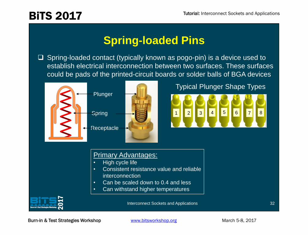
Spring-loaded Pins
32
Spring-loaded contact (typically known as pogo-pin) is a device used to
establish electrical interconnection between two surfaces. These surfaces
could be pads of the printed-circuit boards or solder balls of BGA devices
1 2 3 4 5 6 7 8
Plunger
Receptacle
Spring
Typical Plunger Shape Types
Primary Advantages:• High cycle life
• Consistent resistance value and reliable
interconnection
• Can be scaled down to 0.4 and less
• Can withstand higher temperatures
Interconnect Sockets and Applications

Tutorial: Interconnect Sockets and ApplicationsBiTS 2017
March 5-8, 2017Burn-in & Test Strategies Workshop www.bitsworkshop.org
Stamped-and-Formed Contacts
33
Typical Process: Made from reels of flat stock
material
Strips run through stamping
and forming die to form
socket contacts
Contacts are electro-plated
and inserted into the housing
Example of stamped and formed
contacts on a carrier strip
Primary Advantages: • Low-cost
• High-volume application
• Applications include production
sockets, crimped contacts, etc.
cLGA®
Dual-compression contactCourtesy: Amphenol InterCon Systems
Interconnect Sockets and Applications

Tutorial: Interconnect Sockets and ApplicationsBiTS 2017
March 5-8, 2017Burn-in & Test Strategies Workshop www.bitsworkshop.org
Pin and Socket Contacts
34
Pin and socket type of contacts are
typically made on a screw machine
They are comprised of two parts –
Female receptacle and Male header
Standard contacts can be inserted into
a variety of housings to create IO
connectors, sockets and board-to-board
connectors.
Primary Advantages:• Consistent and reliable contact
resistance
• Low tooling cost
• Medium cycle life (insertion/removal)
• Application includes validation socket
and board to board interconnect
Female Receptacle Male Header
Courtesy: Advanced
Interconnection
Interconnect Sockets and Applications

Tutorial: Interconnect Sockets and ApplicationsBiTS 2017
March 5-8, 2017Burn-in & Test Strategies Workshop www.bitsworkshop.org
Made from 2D MEMs process
Contacts are plated
One end is soldered down
Tips puncture into silicon (Cu)
bump
Example of vertical interconnect
assembled to probe card
Primary Advantages:• Low force <10gf
• Ultra-fine pitch <150um
• High cycle life
• Application include silicon testing
MEMs-based Vertical Interconnect
35
Courtesy: FormFactor Inc
Probe Card
Interconnect Sockets and Applications
Tutorial: Interconnect Sockets and ApplicationsBiTS 2017
March 5-8, 2017Burn-in & Test Strategies Workshop www.bitsworkshop.org
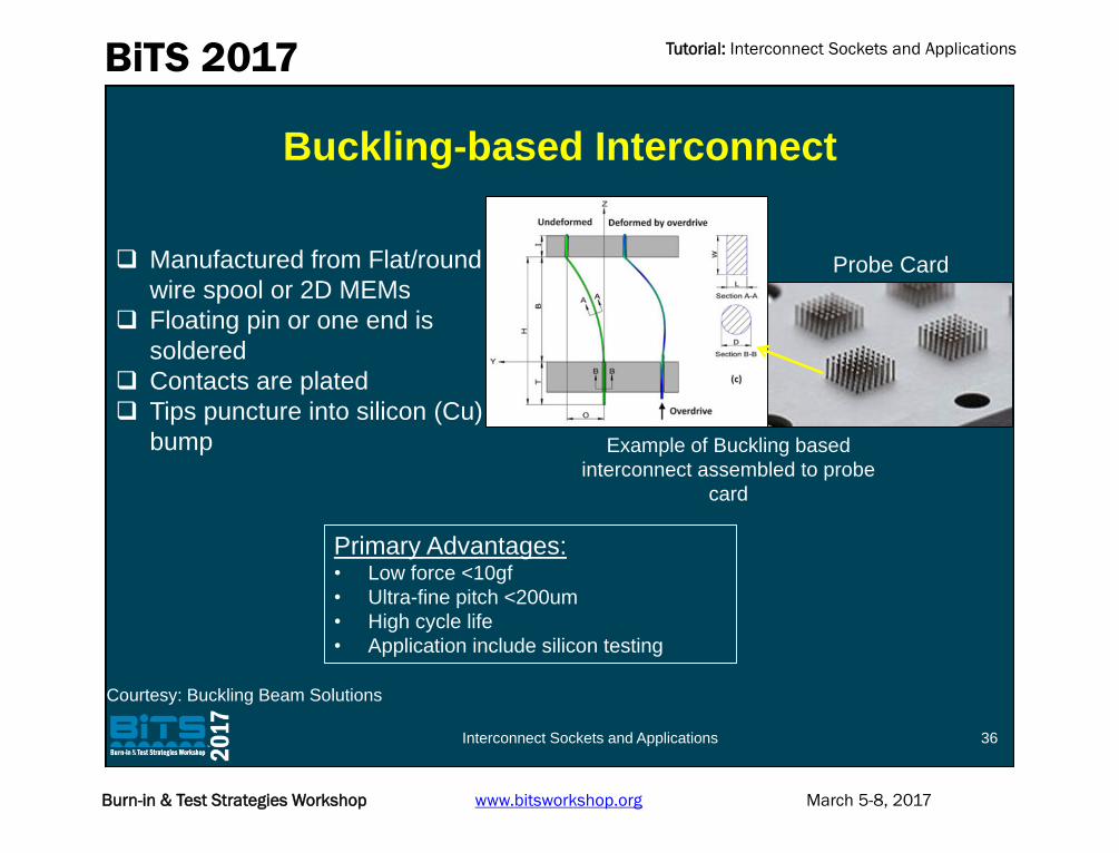
Manufactured from Flat/round
wire spool or 2D MEMs
Floating pin or one end is
soldered
Contacts are plated
Tips puncture into silicon (Cu)
bump Example of Buckling based
interconnect assembled to probe
card
Primary Advantages:• Low force <10gf
• Ultra-fine pitch <200um
• High cycle life
• Application include silicon testing
Buckling-based Interconnect
36
Courtesy: Buckling Beam Solutions
Probe Card
Interconnect Sockets and Applications

Tutorial: Interconnect Sockets and ApplicationsBiTS 2017
March 5-8, 2017Burn-in & Test Strategies Workshop www.bitsworkshop.org
Summary
37
Type of Contact Benefits
Polymer-based contacts (filled with metal
powder) individual contacts
-Electrical characteristics
-Can be scaled down to <0.4mm
Polymer-based conductive sheet -Electrical Characteristics, Can be scaled down to
<0.4mm, Alignment of sheet to the pads
Polymer based contacts with metal spring
element
-Higher cycle life than metal-filled polymer,
Consistence resistance value
Particle Interconnect -Electrical Characteristics, Can be scaled down to
<0.4mm,Custom and mixed pitch
Spring-loaded Contacts -High cycle life, scaled down to <0.4mm,
consistence resistance
Stamped and formed contacts -Low cost, High-volume application, consistence
resistance
Pin and Socket Contact -Consistence resistance, low tooling cost
MEMs-based Vertical Interconnect -High cycle life, low force, ultra fine pitch <0.15mm
Buckling-based Interconnect -High cycle life, low force, ultra fine pitch <0.20mm
Interconnect Sockets and Applications

Tutorial: Interconnect Sockets and ApplicationsBiTS 2017
March 5-8, 2017Burn-in & Test Strategies Workshop www.bitsworkshop.org
Section 4
Contact Element Material
38Interconnect Sockets and Applications

Tutorial: Interconnect Sockets and ApplicationsBiTS 2017
March 5-8, 2017Burn-in & Test Strategies Workshop www.bitsworkshop.org
Contact Material Selection Factors
Material Availability
Specific Performance
Manufacturability
Cost Effectiveness
39Interconnect Sockets and Applications

Tutorial: Interconnect Sockets and ApplicationsBiTS 2017
March 5-8, 2017Burn-in & Test Strategies Workshop www.bitsworkshop.org
Socket Contact Selection
40
2. Define socket contact requirements
3.Select contact material
1. Understand Industry Trends
High-level Selection Flow
Interconnect Sockets and Applications

Tutorial: Interconnect Sockets and ApplicationsBiTS 2017
March 5-8, 2017Burn-in & Test Strategies Workshop www.bitsworkshop.org
Contact size• Pitch (Center to center spacing)
• Tighter tolerances
1. Understand Industry Trends
Pitch
0
0.2
0.4
0.6
0.8
1
1.2
1.4
2002 2004 2006 2008 2010 2012 2014 2016 2017
Decrease in Ball Pitch Over Time
Year
Pitch
in
mm
Package
Solder -ball
41Interconnect Sockets and Applications

Tutorial: Interconnect Sockets and ApplicationsBiTS 2017
March 5-8, 2017Burn-in & Test Strategies Workshop www.bitsworkshop.org
1. Understand Industry Trends (Cont’d.)
Lower normal force
• Minimize deflection of the socket substrate, mechanical
hardware and PCB
• Meet reliability requirements
Growing number of pins/socket
• Exceeding 100 contacts/inch and exceeding 2,000
contacts/socket
The normal force is perpendicular
to the surfaces in contact F
F
42Interconnect Sockets and Applications

Tutorial: Interconnect Sockets and ApplicationsBiTS 2017
March 5-8, 2017Burn-in & Test Strategies Workshop www.bitsworkshop.org
1. Understand Industry Trends (Cont’d.)
43
Single or Dual-compression mount• Reliable solder joint (for single compression mount)
• Provide repeated insertion removal cycles without taking
a set
Higher operating temperatures• Infotainment systems > 130ºC
Shorter development and Manufacturing lead time• Faster to design and faster to manufacture
Price• Lower product cost
Interconnect Sockets and Applications

Tutorial: Interconnect Sockets and ApplicationsBiTS 2017
March 5-8, 2017Burn-in & Test Strategies Workshop www.bitsworkshop.org
2. Define Socket Contact Requirements
2a. Mechanical
2b. Electrical
2c. Material
2d. Attachment Process
2e. Environment
44Interconnect Sockets and Applications

Tutorial: Interconnect Sockets and ApplicationsBiTS 2017
March 5-8, 2017Burn-in & Test Strategies Workshop www.bitsworkshop.org
2a. Mechanical Requirements
Mating surface material and contact area
• PCB mating surface , Device (BGA) mating
surface
Contact material geometry
• Contact area
• Contact normal force
• Insertion/extraction force
45Interconnect Sockets and Applications
Norm
aliz
ed
Forc
e
Norm
aliz
ed
Resis
tance
Normalized
Compression
Tech1
ResistanceTech2
ResistanceTech3
Resistance
Tech1
Force
Tech2
Force
Tech3
Force
Resistance
Knee
0.1 0.2 0.3 0.4 0.5 0.6 0.7 0.8 0.9 1
0.1
0
.2 0.3
0.4
0.5
0.6
0.7
0.8
0.9
1
0.1
0
.2 0.3
0.4
0.5
0.6
0.7
0.8
0.9
1

Tutorial: Interconnect Sockets and ApplicationsBiTS 2017
March 5-8, 2017Burn-in & Test Strategies Workshop www.bitsworkshop.org
2b. Electrical Requirements
Total socket resistance
• Contact resistance
• Bulk resistance
Current carrying capacity
• Higher conductivity materials allow greater current
flow with less temperature rise
• Current carrying capacity depends on contact
geometry, contact material and normal force
46
Ri-
ball
Ri
Ri-pad
Interconnect Sockets and Applications

Tutorial: Interconnect Sockets and ApplicationsBiTS 2017
March 5-8, 2017Burn-in & Test Strategies Workshop www.bitsworkshop.org
2b. Electrical Requirements (Cont’d.)
Signal Properties
• Signal to ground ratio -- ratio determines connector
noise
• Capacitance – energy stored in an electrical field
between two charged objects – coupling between two
conductors
• Impedance -- The ratio of voltage to current of an
electrical signal propagating through a circuit
component.
Interconnect Sockets and Applications 47

Tutorial: Interconnect Sockets and ApplicationsBiTS 2017
March 5-8, 2017Burn-in & Test Strategies Workshop www.bitsworkshop.org
2b. Electrical Requirements (Cont’d.)
Signal Properties
• Inductance -- Energy stored in a magnetic field
generated by the current looping through an electrical
circuit.
• Propagation delay -- The signal delay caused by the
connector capacitance. Reduced connector length
reduces the propagation delay.
• Cross-talk -- Signals from one line leaking into
another conductor because of capacitance or
inductive coupling or both.
Interconnect Sockets and Applications 48

Tutorial: Interconnect Sockets and ApplicationsBiTS 2017
March 5-8, 2017Burn-in & Test Strategies Workshop www.bitsworkshop.org
2c. Material Requirement
Primary required properties
• Low contact and bulk electrical resistance
• Corrosion resistance
• Low frictional forces – reduces wear and increases
cycle life
• Good spring properties
• Lower cost
Typical base contact material
• Metal – Copper alloys
• Elastomer – Silicon rubber
Interconnect Sockets and Applications 49

Tutorial: Interconnect Sockets and ApplicationsBiTS 2017
March 5-8, 2017Burn-in & Test Strategies Workshop www.bitsworkshop.org
2c. Material Requirement (Cont’d.)
Base Material requirement:
• Yield strength. Determines beam deflection allowed
within elastic range
• Conductivity – minimized bulk resistance
• Hardness – reduces wear and increases cycle life
Contact interface plating materials:
• Gold (Au)
Hard gold or soft gold over Nickel under-plating.
Hardness is per knoop hardness – electrolytic gold --
30 to 40 micro-inches
ENIG – Immersion gold over Nickel– 3 to 10 micro-
inches of gold
Interconnect Sockets and Applications 50

Tutorial: Interconnect Sockets and ApplicationsBiTS 2017
March 5-8, 2017Burn-in & Test Strategies Workshop www.bitsworkshop.org
2c. Material Requirement (Cont’d.)
Contact Interface Plating Materials:
• Palladium (Pd) and alloys
Usually over-plated with thin soft gold (approx. 10
micro-inches)
Pd and its alloys have higher hardness and
durability than gold (Au)
• Tin (Sn) and its alloys
Thickness ranges depending on the process
Hot dipping
Electro plating
51Interconnect Sockets and Applications

Tutorial: Interconnect Sockets and ApplicationsBiTS 2017
March 5-8, 2017Burn-in & Test Strategies Workshop www.bitsworkshop.org
2c. Material Requirement (Cont’d.)
Contact interface plating materials:
• Silver AgTypically used on the elastomeric contacts – silicon rubber as
base material
• Nickel (Ni)Common material for under-plating
Typical thickness 150 to 200 micro-inches
Types of plating processes:
• Electrolytic plating
• Electroless plating
• Hot Dipping
52Interconnect Sockets and Applications

Tutorial: Interconnect Sockets and ApplicationsBiTS 2017
March 5-8, 2017Burn-in & Test Strategies Workshop www.bitsworkshop.org
2c. Material Requirement (Cont’d.)
Housing Material:
• Typically thermoplastics (polymer-based) is used
to support contacts
Provide environmental protection
• Critical property requirement of housing include:
Withstand soldering temperatures with low
acceptable warpage (Pb-free process)
Dimensional stability
Moisture resistance
53Interconnect Sockets and Applications

Tutorial: Interconnect Sockets and ApplicationsBiTS 2017
March 5-8, 2017Burn-in & Test Strategies Workshop www.bitsworkshop.org
2d. Contact Attachment Process
54
1. Soldering to PCB, mechanically attaching to device
BGA DeviceBGA Single-compression
Socket
Motherboard
Soldered-down Socket
Top clamping plate
Bottom Plate
F
F
2. Mechanically attaching to PCB and Device
BGA Device
Dual-compression Socket
BGA Dual-Compression
Socket
Top clamping plate
Bottom Plate
F
F
Interconnect Sockets and Applications

Tutorial: Interconnect Sockets and ApplicationsBiTS 2017
March 5-8, 2017Burn-in & Test Strategies Workshop www.bitsworkshop.org
2d. Contact Attachment Process (Cont’d.)
1. Soldering to PCB, mechanically attaching to device
• Solder process
Convection reflow
Vapor-phase reflow
Manual soldering
Wave soldering
• Mechanical attaching to device
Requires custom hardware to make connectivity
through compression
55
Socket soldered to PCB
Mechanical Hardware
PCB
Interconnect Sockets and Applications

Tutorial: Interconnect Sockets and ApplicationsBiTS 2017
March 5-8, 2017Burn-in & Test Strategies Workshop www.bitsworkshop.org
2d. Contact Attachment Process (Cont’d.)
2. Mechanical Attachment to PCB
• Solderless contacts. Compression mount on both PCB and
device end
• Require custom hardware to make connectivity to PCB
and device through compression
• Require higher force to make electrical connection than
soldering one end and mechanically attaching other
56
Courtesy: Ironwood Electronics
Mechanical Hardware
Dual Compression,
solderless socket
Interconnect Sockets and Applications
Tutorial: Interconnect Sockets and ApplicationsBiTS 2017
March 5-8, 2017Burn-in & Test Strategies Workshop www.bitsworkshop.org
2e. Contact Environmental Requirements
Common applications include:
• Consumer
• Automotive
• Aircraft
• Military
• Computer
• Telecommunication
57Interconnect Sockets and Applications

Tutorial: Interconnect Sockets and ApplicationsBiTS 2017
March 5-8, 2017Burn-in & Test Strategies Workshop www.bitsworkshop.org
58
Typical operating temperature conditions
– Can vary depending on application
Typical life – Can
vary depending on
application
Category Minimum ºC Maximum ºC Approx. Years
Consumer 0 +100 ~ 3
Computer 0 +100 ~5
Automotive -50 +100 to +150 ~10
Aircraft -50 +125 ~20
Military -50 +125 ~10
Telecommunication -40 +100 ~15
Types of Tests:
Temperature and humidity
Gaseous
Vibration
Shock
2e. Contact Environmental Requirements
(Cont’d.)
Interconnect Sockets and Applications

Tutorial: Interconnect Sockets and ApplicationsBiTS 2017
March 5-8, 2017Burn-in & Test Strategies Workshop www.bitsworkshop.org
3. Contact Material Selection
Contact material plays a significant role in
design optimization
59
Primary Requirements Contact Material Property
• Cycle life/Durability • Contact finish, Resistance to taking set
• Reliability • Contact finish, Stress relaxation
• SI and Current carrying
capacity
• Electrical and thermal conductivity
• Deflection under load • Modulus of elasticity, yield strength
• Normal force • Modulus of elasticity, mechanical
tolerances
Interconnect Sockets and Applications

Tutorial: Interconnect Sockets and ApplicationsBiTS 2017
March 5-8, 2017Burn-in & Test Strategies Workshop www.bitsworkshop.org
Section 5Printed Circuit Board (PCB) &
Hardware Requirement
60Interconnect Sockets and Applications

Tutorial: Interconnect Sockets and ApplicationsBiTS 2017
March 5-8, 2017Burn-in & Test Strategies Workshop www.bitsworkshop.org
Overview:
• PCB surface finish plays an important role in
achieving reliable interconnection between the
component or device and bare PCB
PCB Surface Finishes
61Interconnect Sockets and Applications

Tutorial: Interconnect Sockets and ApplicationsBiTS 2017
March 5-8, 2017Burn-in & Test Strategies Workshop www.bitsworkshop.org
PCB Surface Finishes (Cont’d.)
The primary purpose of the surface finish
are:
• Connectivity between the PCB and component
devices
• Protect the copper area from oxidation prior to
assembly (soldering or using interconnect
sockets)
• Promote reliable interconnection for long-term
performance
62Interconnect Sockets and Applications

Tutorial: Interconnect Sockets and ApplicationsBiTS 2017
March 5-8, 2017Burn-in & Test Strategies Workshop www.bitsworkshop.org
PCB Surface Finishes (Cont’d.)
Two types of PCB pads:
1. Copper defined: Solder-mask opening larger than
the metal pad
2. Solder-mask defined: Metal pad larger than the
solder-mask opening
63
Copper-defined Pads Mask-defined Pads
Interconnect Sockets and Applications

Tutorial: Interconnect Sockets and ApplicationsBiTS 2017
March 5-8, 2017Burn-in & Test Strategies Workshop www.bitsworkshop.org
Primary Factors in Selecting PCB Finish
Cost
RoHS compliant
Assembly methods
Durability
Environment
Shelf life
Testability
Reliability
64Interconnect Sockets and Applications

Tutorial: Interconnect Sockets and ApplicationsBiTS 2017
March 5-8, 2017Burn-in & Test Strategies Workshop www.bitsworkshop.org
Types of Surface Finishes
Standard Hot Air Solder Level (HASL) & Lead-
Free HASL
Organic Solderability Preservative (OSP)
Immersion Silver
Immersion Tin
Gold:
• Gold – ENIG -Electroless Nickel Immersion Gold
• Hard Gold
Electroless Nickel Electroless Palladium
Immersion Gold (ENEPIG)
65Interconnect Sockets and Applications

Tutorial: Interconnect Sockets and ApplicationsBiTS 2017
March 5-8, 2017Burn-in & Test Strategies Workshop www.bitsworkshop.org
Standard HASL and Lead-Free HASL
Typical Finish:
• Standard HASL: Typically Tin-Lead (Sn-Pb)
Melts at 183ºC
Shelf life: >12 months – very good
• Lead-free HASL: Typically Tin-Copper (Sn-Ag-Cu),
Tin-Copper-Nickel (Sn-Cu-Ni)
Melts at 217ºC to 228ºC
Shelf life: approx. 12 months
Typical Thickness:
• 70-200 micro-inches
• IPC specifies complete coverage of SMT pads
66Interconnect Sockets and Applications

Tutorial: Interconnect Sockets and ApplicationsBiTS 2017
March 5-8, 2017Burn-in & Test Strategies Workshop www.bitsworkshop.org
Standard HASL and Lead-Free HASL
(Cont’d.)
Advantages:
• Low cost
• Readily and widely available
• Easy to rework – Low cost
Disadvantages:
• Uneven surface
• Not good for direct socket interconnection
• Not good for thermal shock
• Potential of solder bridging is high
High-level Typical Process: Clean Microetch Apply Flux Solder Dip Knife leveling
Rinsing 67Interconnect Sockets and Applications

Tutorial: Interconnect Sockets and ApplicationsBiTS 2017
March 5-8, 2017Burn-in & Test Strategies Workshop www.bitsworkshop.org
Organic Solderability Preservatives
(OSP)
Typical Finish
• Organic Solderability Preservatives
• Applied directly on Copper
Typical Thickness:
• Thin coating : 4-20 micro-inches
• Finish typically is not specified on the fab drawing
68Interconnect Sockets and Applications

Tutorial: Interconnect Sockets and ApplicationsBiTS 2017
March 5-8, 2017Burn-in & Test Strategies Workshop www.bitsworkshop.org
Organic Solderability Preservatives
(OSP) (Cont’d.)
Advantages:• Lead-free
• Flat and planar surface
• Simple process and easy to manufacture
• Easy to rework – Low cost
Disadvantages:• Short shelf life, less than 6 months
• Exposed Copper during final assembly
• Bare exposed Copper can cause socket interconnect reliability
issues
High-level Typical Process:• Clean Microetch Flood OSP Rinse
69Interconnect Sockets and Applications
Tutorial: Interconnect Sockets and ApplicationsBiTS 2017
March 5-8, 2017Burn-in & Test Strategies Workshop www.bitsworkshop.org
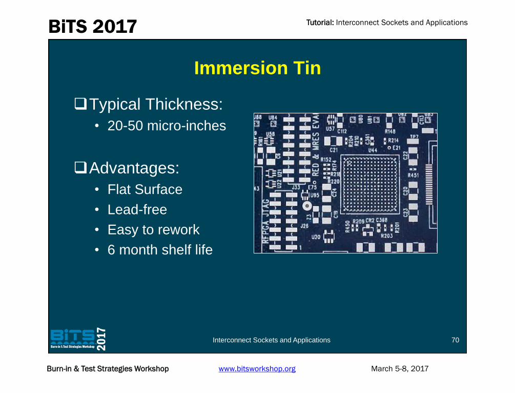
Immersion Tin
Typical Thickness:
• 20-50 micro-inches
Advantages:
• Flat Surface
• Lead-free
• Easy to rework
• 6 month shelf life
70Interconnect Sockets and Applications

Tutorial: Interconnect Sockets and ApplicationsBiTS 2017
March 5-8, 2017Burn-in & Test Strategies Workshop www.bitsworkshop.org
Immersion Tin (Cont’d.)
Disadvantages:
• High potential for damage during handling
• Exposed tin can corrode – cause interconnect socket
issues during direct socket connection
• Tin whiskers
High-level Typical Process:
• Clean Microetch Predip Apply Tin Post dip
Rinse
71Interconnect Sockets and Applications

Tutorial: Interconnect Sockets and ApplicationsBiTS 2017
March 5-8, 2017Burn-in & Test Strategies Workshop www.bitsworkshop.org
Gold – ENIG
Typical Thickness:
• Nickel: 100-200 micro-inches
• Gold: 3-10 micro-inches
Advantages:
• Flat Surface
• Lead-free
• Approx. 12 month shelf life
• Good for direct socket interconnection
72Interconnect Sockets and Applications

Tutorial: Interconnect Sockets and ApplicationsBiTS 2017
March 5-8, 2017Burn-in & Test Strategies Workshop www.bitsworkshop.org
Disadvantages:
• Medium high cost
• Not reworkable
• Complicated process
High-level Typical Process
• Clean Microetch Catalyst Electroless Nickel
Rinse Immersion Gold Rinse
73
Gold – ENIG (Cont’d.)
Interconnect Sockets and Applications

Tutorial: Interconnect Sockets and ApplicationsBiTS 2017
March 5-8, 2017Burn-in & Test Strategies Workshop www.bitsworkshop.org
Gold – Hard Gold
Typical Thickness:
• Nickel: 125-150 micro-inches
• Gold: 25-30 micro-inches
Advantages:
• Durable surface
• Lead-free
• Excellent for direct socket interconnection
• Long shelf life
74Interconnect Sockets and Applications

Tutorial: Interconnect Sockets and ApplicationsBiTS 2017
March 5-8, 2017Burn-in & Test Strategies Workshop www.bitsworkshop.org
Disadvantages:
• Very high cost
• Extra processing labor intensive
• Plating / Bus bars
High-level Typical Process:
Apply Resist Clean Microetch Electroless
Nickel Rinse Electrolytic Gold Rinse Strip
Resist Clean
75
Gold – Hard Gold (Cont’d.)
Interconnect Sockets and Applications
Tutorial: Interconnect Sockets and ApplicationsBiTS 2017
March 5-8, 2017Burn-in & Test Strategies Workshop www.bitsworkshop.org
Immersion Silver
76
Typical Thickness:• 8-15 micro-inches of pure Silver
Advantages:• Excellent Solderability
• Good for direct socket interconnect
• 6-12months shelf life
Disadvantages:• Sensitive to handling
• Medium High cost
High-level Typical Process:• Clean Microetch Electroless Nickel Rinse Immersion
Silver Rinse
Interconnect Sockets and Applications
Tutorial: Interconnect Sockets and ApplicationsBiTS 2017
March 5-8, 2017Burn-in & Test Strategies Workshop www.bitsworkshop.org
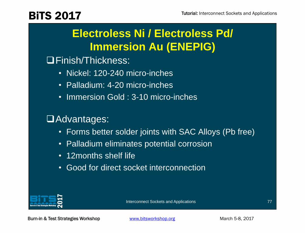
Electroless Ni / Electroless Pd/
Immersion Au (ENEPIG)
77
Finish/Thickness:
• Nickel: 120-240 micro-inches
• Palladium: 4-20 micro-inches
• Immersion Gold : 3-10 micro-inches
Advantages:
• Forms better solder joints with SAC Alloys (Pb free)
• Palladium eliminates potential corrosion
• 12months shelf life
• Good for direct socket interconnection
Interconnect Sockets and Applications

Tutorial: Interconnect Sockets and ApplicationsBiTS 2017
March 5-8, 2017Burn-in & Test Strategies Workshop www.bitsworkshop.org
Disadvantages:
• Does not form good joints with Sn/Pb alloys
• High cost
High-level Typical Process:
• Clean Microetch Electroless Nickel
Electroless Palladium Immersion Au
78
Electroless Ni / Electroless Pd/
Immersion Au (ENEPIG) (Cont’d.)
Interconnect Sockets and Applications

Tutorial: Interconnect Sockets and ApplicationsBiTS 2017
March 5-8, 2017Burn-in & Test Strategies Workshop www.bitsworkshop.org
Comparison of Surface Finishes
Type Planarity Solderability Dual Compression
Contact
Typical
Cost
HASL Poor Good Poor Low
OSP Good Good Poor Low
Immersion Tin Good Good Poor Low
Immersion Ag Good Good Good Medium
Gold - ENIG Good Good Very Good Medium
Gold-Hard Gold Good Good Excellent Very High
ENEPIG Good Good Excellent High
79Interconnect Sockets and Applications

Tutorial: Interconnect Sockets and ApplicationsBiTS 2017
March 5-8, 2017Burn-in & Test Strategies Workshop www.bitsworkshop.org
Overview of PCB Solder-mask
80
Primary Purpose of Solder-mask:• Prevent solder shorts under components
• Prevent socket interconnect shorts
• Prevent corrosion to underlying circuitry
• Plating resist for surface finishes
Copper-defined Pads Mask-defined Pads
Interconnect Sockets and Applications

Tutorial: Interconnect Sockets and ApplicationsBiTS 2017
March 5-8, 2017Burn-in & Test Strategies Workshop www.bitsworkshop.org
Solder-mask Considerations for Socket
Connectivity
• Feature size of the solder-mask
• Registration of the solder-mask
• Tolerance on the feature size
• Thickness of the solder-mask
Interconnect Sockets and Applications 81
Typical Solder-mask Process
Solder-
mask
Direct
Imaging
Indirect
Imaging
Screen
PrintInk
Jet
LDI
Laser
Direct
Imaging
LPI
Liquid
PhotoImageable
Dry Film

Tutorial: Interconnect Sockets and ApplicationsBiTS 2017
March 5-8, 2017Burn-in & Test Strategies Workshop www.bitsworkshop.org
Importance of Solder-mask (SM)
Registration
82
SM Tolerance Considerations
-- Size
-- Position
-- Thickness (primarily for sockets
with short working range)
Exposed trace
Contact Pad Contact Pad
Via Pad
Solder-mask mis-
registration
Exposed Via
Pad
Potential Socket contact short in this area
Exposed
trace
Interconnect Sockets and Applications

Tutorial: Interconnect Sockets and ApplicationsBiTS 2017
March 5-8, 2017Burn-in & Test Strategies Workshop www.bitsworkshop.org
PCB Mechanical Keep-out for Socket
Parameters to include
in fab drawing• Alignment hole location
• Socket body/frame
• Mounting hole location
• Surface mount components around the socket body/frame
• Pad diameter
• Surface Finish
83
Socket outline
Hardware
outline
Hardware mounting
holes 4X
Socket alignment holes
2X
Surface mount components max
height 2mmInterconnect Sockets and Applications

Tutorial: Interconnect Sockets and ApplicationsBiTS 2017
March 5-8, 2017Burn-in & Test Strategies Workshop www.bitsworkshop.org
Section 6
Electrical Requirements
84Interconnect Sockets and Applications

Tutorial: Interconnect Sockets and ApplicationsBiTS 2017
March 5-8, 2017Burn-in & Test Strategies Workshop www.bitsworkshop.org
Impedance of the Socket
In simple form, impedance (Zo) can be expressed
in terms of inductance and capacitance
• Zo = sqrt (L/C) (lossless impedance equation)
• L (pin inductance) is a function of the pin geometry,
socket pitch and pin length
• C (pin capacitance) is a function of the pin geometry,
socket pitch, pin length and dielectric material
Impedance matching to system interconnect is
essential in minimizing return loss for high-speed
applications
85Interconnect Sockets and Applications

Tutorial: Interconnect Sockets and ApplicationsBiTS 2017
March 5-8, 2017Burn-in & Test Strategies Workshop www.bitsworkshop.org
Equivalent Circuit of the Socket
86
• To accurately model or calculate
the impedance of one pin, the
surrounding pins need to be
accounted for
Example of BGA socket equivalent circuit
( 2 pins are shown)
Notation:
C12a (BGA side): mutual capacitance between adjacent pins
C12b (PCB side): mutual capacitance between adjacent pins
L1, L2: pin inductances
M12: mutual inductance
R1, R2: pin resistances
L1 L2
R1 R2
C12b
C12a
M12
Interconnect Sockets and Applications

Tutorial: Interconnect Sockets and ApplicationsBiTS 2017
March 5-8, 2017Burn-in & Test Strategies Workshop www.bitsworkshop.org
Socket Pin Insertion Loss
87
• Insertion loss is
proportional to socket pin
length and contact
resistance
• The longer the pin, the
higher insertion loss for
the same material
• The socket material also
plays a role in insertion
loss
• The lower loss material
yields lower insertion loss
-3
-2.5
-2
-1.5
-1
-0.5
0
0 2 4 6 8 10 12 14 16 18 20
Inse
rtio
n L
oss
(dB
)
Frequency (GHz)
Insertion Loss (dB)
Socket A Socket B Socket C
Socket Height: Socket A < Socket B < Socket C
Bet
ter
Low Insertion is preferred for signal integrity performance
Interconnect Sockets and Applications

Tutorial: Interconnect Sockets and ApplicationsBiTS 2017
March 5-8, 2017Burn-in & Test Strategies Workshop www.bitsworkshop.org
Socket Pin-to-Pin Cross-Talk
88
• Cross-talk is proportional
to the socket pin length
• The longer the pin length,
the higher the cross-talk
• It is critical to have a low
height socket for high-
speed applications
• Socket signal pin-map
also plays a critical role in
reducing cross-talk
• The higher signal-to-gnd
ratio, the lower the cross-
talk
-80
-70
-60
-50
-40
-30
-20
-10
0
0 2 4 6 8 10 12 14 16 18 20
Cro
ss-T
alk (
dB
)
Frequency (GHz)
Cross-Talk
Socket A Socket B Socket C
Socket Height: Socket A < Socket B < Socket C
Bet
ter
Minimal Cross-Talk is preferred for signal integrity performance
Interconnect Sockets and Applications

Tutorial: Interconnect Sockets and ApplicationsBiTS 2017
March 5-8, 2017Burn-in & Test Strategies Workshop www.bitsworkshop.org
Current Carrying Capacity
Current carrying capacity is a very important
electrical requirement of a socket. It must meet
an application requirement for reliable
operations
The ability of socket pin contact to carry current
is primarily limited by the maximum allowable
operating temperature and the pin contact
material and contact geometry
89Interconnect Sockets and Applications

Tutorial: Interconnect Sockets and ApplicationsBiTS 2017
March 5-8, 2017Burn-in & Test Strategies Workshop www.bitsworkshop.org
Section 7
Interconnect Socket and System
Design
90Interconnect Sockets and Applications

Tutorial: Interconnect Sockets and ApplicationsBiTS 2017
March 5-8, 2017Burn-in & Test Strategies Workshop www.bitsworkshop.org
Types of Interconnect Systems
Two Types of Interconnect Systems
1. Load-based System Required compression of the contact material is
achieved by applying measured load using
mechanical hardware system
Typically used where contacts have low working
range
2. Deflection-based System Required compression of the contact material is
achieved by using a fixed mechanical stopper
Typically used where contacts have high working
range
91Interconnect Sockets and Applications

Tutorial: Interconnect Sockets and ApplicationsBiTS 2017
March 5-8, 2017Burn-in & Test Strategies Workshop www.bitsworkshop.org
Load-based System
F F
F
Socket contact
Top clamp
PCB
Socket
Deflection
F
Spring x 2
Bottom Clamp
Example:
Polymer socket contacts-- Typical working range < 0.005”
LGA Package
92Interconnect Sockets and Applications
Schematic

Tutorial: Interconnect Sockets and ApplicationsBiTS 2017
March 5-8, 2017Burn-in & Test Strategies Workshop www.bitsworkshop.org
Load-based System (Cont’d.)Uncompressed
Compressed
Primary Advantages:• Typically use spring screw
retention system
• Spring accounts for
thickness variations in
retention system, socket,
and package
Limitations:• High BOM cost
• Typically used for sockets
with low working range
<200um
93Interconnect Sockets and Applications

Tutorial: Interconnect Sockets and ApplicationsBiTS 2017
March 5-8, 2017Burn-in & Test Strategies Workshop www.bitsworkshop.org
Deflection-based System
94
F F
F F
Deflection
Top Clamp
LGA Package
Bottom Clamp
Socket
Socket contact
PCB
Example:-- Pogo pins, stamped and formed contacts -- Typical working range = 0.010”-0.015”
Interconnect Sockets and Applications
Schematic

Tutorial: Interconnect Sockets and ApplicationsBiTS 2017
March 5-8, 2017Burn-in & Test Strategies Workshop www.bitsworkshop.org
Deflection Based System (Cont’d.)
Interconnect Sockets and Applications 95
Uncompressed
Compressed
Primary Advantages:• Socket acts as compliant
member accommodating
thickness variation in
retention parts
• Low BOM cost
Limitations:• Typically used for sockets
with high working range
>250um
• Typically use a pattern for
tightening retention screws
• Require tight thickness and
flatness control for
retention hardware

Tutorial: Interconnect Sockets and ApplicationsBiTS 2017
March 5-8, 2017Burn-in & Test Strategies Workshop www.bitsworkshop.org
Socket Design Parameters
Thermo-Mechanical
• Compression and Force
• Cycle life / durability
• Operating temperature
• BGA vs LGA
• Pitch
• PCB keep-out and plating
• Hard stops preventing pin over-compression
96Interconnect Sockets and Applications
Tutorial: Interconnect Sockets and ApplicationsBiTS 2017
March 5-8, 2017Burn-in & Test Strategies Workshop www.bitsworkshop.org
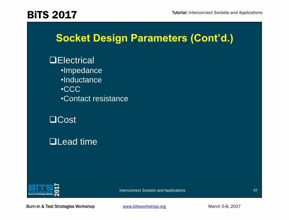
Socket Design Parameters (Cont’d.)
97
Electrical•Impedance
•Inductance
•CCC
•Contact resistance
Cost
Lead time
Interconnect Sockets and Applications

Tutorial: Interconnect Sockets and ApplicationsBiTS 2017
March 5-8, 2017Burn-in & Test Strategies Workshop www.bitsworkshop.org
Mechanical Hardware Design
98
Spring Screw Retention
accommodate z-stack
tolerances
Split loading for bare die
devices
• Periphery loading
• Heat sink loading
Stiffener plate insulator
openings accommodate surface
mount components bottom side
of PCB
Top plate insulator openings
accommodate surface mount
components on DUT Stiffener plate
Stiffener plate
insulator
PCB
Socket
DUT
Total load cell
spring 4X
Heat sink
Top plate
Interconnect Sockets and Applications

Tutorial: Interconnect Sockets and ApplicationsBiTS 2017
March 5-8, 2017Burn-in & Test Strategies Workshop www.bitsworkshop.org
Mechanical Tolerances
Z-stack tolerance analysis:• Spring based loading: Spring compressed height variation
• Displacement based loading: Interconnect compressed height
variation
XY tolerance analysis:• Alignment accuracy of interconnect pin to PCB pad
• Alignment accuracy of interconnect pin to Device ball or pad
Monte Carlo based: David Shia, Intel Corporation; 2007
Burn-in and Test Socket Workshop
https://www.bitsworkshop.org/archive/archive2007/2007s6.pdf
• For HVM test, alignment accuracy and repeatability of handler
99Interconnect Sockets and Applications

Tutorial: Interconnect Sockets and ApplicationsBiTS 2017
March 5-8, 2017Burn-in & Test Strategies Workshop www.bitsworkshop.org
Mechanical Z-Tolerance: Example
Z-stack tolerance analysis:
• Spring based loading: Spring compressed height
variation
100
# Component
Nominal
Dimension
(mm)
Tolerance
+/- (mm)Cpk n-σ 1-σ
1 Compressed socket height -1 0.025 1.33 4 0.006
2Package Substrate
thickness-0.75 0.05 1.33 4 0.013
3 Top plate insulator -1 0.1 1.33 4 0.025
4 Top plate thickness -2.5 0.1 1.33 4 0.025
5 Shoulder screw height 18 0.1 1.33 4 0.025
Compressed spring height 12.75 0.375 Worst Case
0.046 RSS(1σ)
0.137 RSS(3σ)
0.182 RSS(4σ)
Sectional
view
12 3
4
5
Interconnect Sockets and Applications

Tutorial: Interconnect Sockets and ApplicationsBiTS 2017
March 5-8, 2017Burn-in & Test Strategies Workshop www.bitsworkshop.org
Force-Deflection Analysis
Finite Element Analysis is used for:
• Optimization (thickness) of mechanical hardware
components (stiffener plate, top plate, etc)
• Interconnect array deflection distribution to ensure
min deflection meets CRES criterion
• Device warpage under mechanical load, thermal load,
etc
Commercially available tools
• ANSYS, Mechanica, Abaqus, etc.
101Interconnect Sockets and Applications

Tutorial: Interconnect Sockets and ApplicationsBiTS 2017
March 5-8, 2017Burn-in & Test Strategies Workshop www.bitsworkshop.org
Force-Deflection Analysis: Example
First order approximation: individual
components of the hardware analyzed
for deflection
Example: Stiffener plate
• Material: Steel; E=200Gpa; ν=0.3; Linear Elastic
• Force: 400N
• Linear Brick element used
• Deflection criterion: 30um max
102
Pressure load
Maximum deflection @ center 27um
Interconnect Sockets and Applications

Tutorial: Interconnect Sockets and ApplicationsBiTS 2017
March 5-8, 2017Burn-in & Test Strategies Workshop www.bitsworkshop.org
Section 8
Socket Interconnect System Testing
103Interconnect Sockets and Applications

Tutorial: Interconnect Sockets and ApplicationsBiTS 2017
March 5-8, 2017Burn-in & Test Strategies Workshop www.bitsworkshop.org
Socket Electrical Measurements
Contact resistance measurement
Signal integrity S-parameters measurements,
which contain the following data:
• Impedance of the socket
• Insertion loss, return Loss
• pin-to-pin cross-talk
104Interconnect Sockets and Applications

Tutorial: Interconnect Sockets and ApplicationsBiTS 2017
March 5-8, 2017Burn-in & Test Strategies Workshop www.bitsworkshop.org
Contact Resistance Measurement
105
Contact resistance board and
package are designed to
validate retention system and
measure pin total resistance
(bulk + contact)
Contact resistance board can
be designed with multiple loops
• Helps in debugging areas which
are electrically open
• Electrical open indicates more
PCB or package deflection.
Insufficient stiffness of back plate
and/or top plate
Package daisy chain
PCB daisy
chain
PCB
Socket
Package
Interconnect Sockets and Applications

Tutorial: Interconnect Sockets and ApplicationsBiTS 2017
March 5-8, 2017Burn-in & Test Strategies Workshop www.bitsworkshop.org
Contact Resistance Measurement
(Cont’d.)
Matching daisy chain package needs to be designed
Package is soldered down to daisy chain board.
Measured resistance is Rsoldered
Total resistance per pin
• (R-Rsoldered)/number of pins
Interconnect Sockets and Applications 106
Over-lay PCB
and package
daisy chain
R
Tutorial: Interconnect Sockets and ApplicationsBiTS 2017
March 5-8, 2017Burn-in & Test Strategies Workshop www.bitsworkshop.org
Contact Resistance Measurement
(Cont’d.)
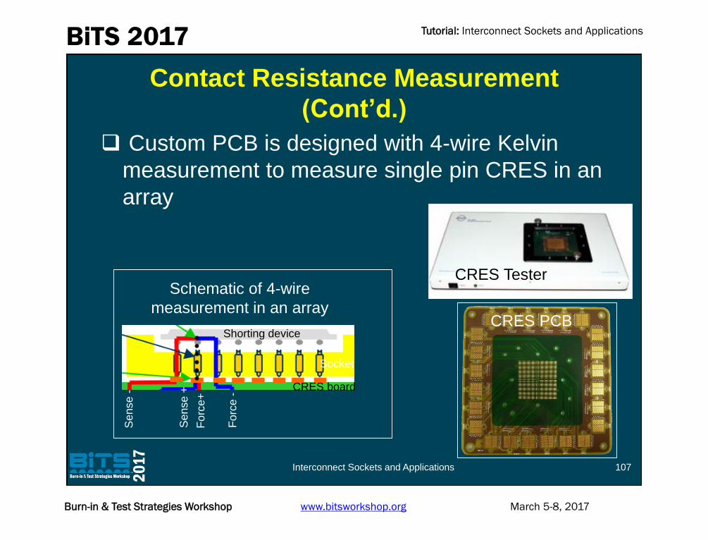
Custom PCB is designed with 4-wire Kelvin
measurement to measure single pin CRES in an
array
107
CRES PCB
CRES TesterSchematic of 4-wire
measurement in an array
Shorting device
Socket
CRES board
Forc
e+
Se
nse +
Fo
rce -
Se
nse
-
Interconnect Sockets and Applications

Tutorial: Interconnect Sockets and ApplicationsBiTS 2017
March 5-8, 2017Burn-in & Test Strategies Workshop www.bitsworkshop.org
Signal Integrity Measurement
Signal integrity S-parameter measurements characterize the
electrical performance of the socket in terms of impedance, insertion
loss, return loss and pin-to-pin cross-talk in frequency domain
Identify a signal test pattern for testing. Examples below show 2-
signal pin and 4-signal pins test patterns
108
2-signal pin test pattern with
1:1 signal-to-gnd ratio
4-signal pin test pattern with
1:1 signal-to-gnd ratio
Signal pin
Ground pin
Interconnect Sockets and Applications

Tutorial: Interconnect Sockets and ApplicationsBiTS 2017
March 5-8, 2017Burn-in & Test Strategies Workshop www.bitsworkshop.org
Signal Integrity Measurement (Cont’d.)
Diagram below shows an example of connecting a VNA
(Vector Network Analyzer) test equipment to test fixtures
measuring the s-parameters of two socket pins through
4-port measurements
109
Port 4Port 3Port 2
Port 1
Top Test Fixture
Bottom Test
Fixture
Test Socket
PCB Test Fixture
SMP Connectors
Interconnect Sockets and Applications

Tutorial: Interconnect Sockets and ApplicationsBiTS 2017
March 5-8, 2017Burn-in & Test Strategies Workshop www.bitsworkshop.org
System Qualification
System Level Validation and testing
• At normal operating conditions
Normal operating conditions; passive heat sink or active
heat sink
Extreme operating conditions; Thermal margining tool
• Long-term aging tests
Environmental chamber – system is subjected to
environmental test conditions
110
Thermal margining
tool for CPU
Interconnect Sockets and Applications

Tutorial: Interconnect Sockets and ApplicationsBiTS 2017
March 5-8, 2017Burn-in & Test Strategies Workshop www.bitsworkshop.org
System Qualification (Cont’d.)
111
System Board
IN OUT
Socket
Package
Thermal
margining tool
Schematic of system test
Exploded view of thermal
margining tool
Interconnect Sockets and Applications

Tutorial: Interconnect Sockets and ApplicationsBiTS 2017
March 5-8, 2017Burn-in & Test Strategies Workshop www.bitsworkshop.org
Maintenance: Repair & Cleaning
Repair
Polymer sockets are harder to repair for damaged contacts
Dual compression pogo-pins can be replaced for bent pins
caused by uneven loading
Cleaning
Cleaning is essential for good CRES
Polymer socket contacts are cleaned using light brush and/or
low pressure dry air
For HVM high volume test sockets, cleaning is done in-situ
using cleaning coupons
For BGA devices there is solder migration from solder ball on to
pin-tips
112Interconnect Sockets and Applications

Tutorial: Interconnect Sockets and ApplicationsBiTS 2017
March 5-8, 2017Burn-in & Test Strategies Workshop www.bitsworkshop.org
Section 9
Real World Example (Team Exercise)
& Summary of Technologies
113Interconnect Sockets and Applications

Tutorial: Interconnect Sockets and ApplicationsBiTS 2017
March 5-8, 2017Burn-in & Test Strategies Workshop www.bitsworkshop.org
Team Exercise
Divide into 4 teams
Each team is given set of requirements
Discuss within team and come up with
socket choice meeting the requirements
Report – out the choice with justification
114Interconnect Sockets and Applications

Tutorial: Interconnect Sockets and ApplicationsBiTS 2017
March 5-8, 2017Burn-in & Test Strategies Workshop www.bitsworkshop.org
Team-A: Requirements
Package parameters:
Package size: 12 mm X 12 mm
Die size: 5 mm X 7 mm
Package pitch: 0.65 mm
LGA pads with ENIPEG plating
Requirements:
• Cycle life: <100 cycles
• Operating temperature: 15ºC to 75ºC
• Electrical length <1.5 mm
• Mechanical hardware: Standalone retention solution
• Low cost
• Lead time <4weeks
115Interconnect Sockets and Applications

Tutorial: Interconnect Sockets and ApplicationsBiTS 2017
March 5-8, 2017Burn-in & Test Strategies Workshop www.bitsworkshop.org
Team-B: Requirements
Package parameters:
Package size: 12 mm X 12 mm
Die size: 5 mm X 7 mm
Package pitch: 0.65 mm
LGA pads with ENIPEG plating
Requirements:
• Cycle life: >100K cycles
• Operating temperature: -10°C to 100°C
• Electrical length < 6 mm
• Handler compatible mechanical hardware for cycling
• Lead time < 12 weeks
116Interconnect Sockets and Applications

Tutorial: Interconnect Sockets and ApplicationsBiTS 2017
March 5-8, 2017Burn-in & Test Strategies Workshop www.bitsworkshop.org
Team-C: Requirements
Package parameters:
Package size: 12 mm X 12 mm
Die size: 5 mm X 7 mm
Package pitch: 0.65 mm
LGA pads with ENIPEG plating
Requirements:
• Cycle life: < 20 cycles
• Operating temperature: -10°C to 100°C
• Electrical length < 5 mm
• Mechanical hardware: Standalone retention
• End of life 5-7 years
• High volume
• Lead time < 24weeks
117Interconnect Sockets and Applications

Tutorial: Interconnect Sockets and ApplicationsBiTS 2017
March 5-8, 2017Burn-in & Test Strategies Workshop www.bitsworkshop.org
Team-D: Requirements
Package parameters:
Package size: 12 mm X 12 mm
Die size: 5 mm X 7 mm
Package pitch: 0.65 mm
LGA pads with ENIPEG plating
Requirements:
• Cycle life: <10K cycles
• Operating temperature: -10 °C to 100°C
• Electrical length < 4 mm
• Handler compatible mechanical hardware for cycling
• Lead time < 12 weeks
118Interconnect Sockets and Applications

Tutorial: Interconnect Sockets and ApplicationsBiTS 2017
March 5-8, 2017Burn-in & Test Strategies Workshop www.bitsworkshop.org
Summary of Socket Technologies
Interconnect Sockets and Applications 119
Relative Comparison of Three Technologies
Factors Polymer-based Screw-Machine Stamped-formed
Typical material Silicon rubber filled
with metal powder
Beryllium Copper Beryllium Copper
Scalability <0.4mm
pitch
Very Good Good Good
Electrical height Low Medium to High Medium
Cost/pin Medium High Low
Wiping action No Yes Yes
Compliance/working
range
Low High High
Cycle life
(insertion/removal)
Low High Medium
Solderability to PCB Poor Good Very Good

Tutorial: Interconnect Sockets and ApplicationsBiTS 2017
March 5-8, 2017Burn-in & Test Strategies Workshop www.bitsworkshop.org
Summary of Socket Technologies (Cont’d.)
Interconnect Sockets and Applications 120
Relative Comparison of Three Technologies
Factors Polymer-based Screw-Machine Stamped-formed
Single Vs Dual
compression
Dual only Single and dual Single and dual
Material compression
set
Medium None Very low
Typical lead time Short Medium Long
Volume application Low to Medium Low High
Tooling/NRE Low Medium High
Real-world application Validation Test Production/Test
Cycle time to design Short to
medium
Short to medium Long
Serviceability Low (difficult) High (easy) Low (difficult)

Tutorial: Interconnect Sockets and ApplicationsBiTS 2017
March 5-8, 2017Burn-in & Test Strategies Workshop www.bitsworkshop.org
Section 10
Design to Production Activities
&
Check-list
121Interconnect Sockets and Applications

Tutorial: Interconnect Sockets and ApplicationsBiTS 2017
March 5-8, 2017Burn-in & Test Strategies Workshop www.bitsworkshop.org
122
# ACTIVITY RELATIVE TIMELINE1 Understand product requirement
2 Create Product Requirement Document
3Research and define type of socket contacts to be used and select
4Design Socket and Mechanical Hardware based on PRD -- Include FEA analysis
5Define PCB requirements and special mechanical tolerances, if any
6Design Test boards for testing sockets --Signal Integrity and contact resistance
7Create detailed mechanical drawings including tolerances
8Obtain quotes, order and receive parts –Socket, hardware, test boards, etc.
9Assemble and test socket assemblies for continuity using test boards
10Test for resistance stability with number of insertions
11Conduct Signal Integrity tests using SI test boards
12Conduct Environmental tests –temperature and humidity cycling
13Revise socket and hardware designs per test results as required
14Finalize drawings and release design for production
Time line depends on the complexity and number of design revisions
Socket Design to Production Activity GANTT
Interconnect Sockets and Applications

Tutorial: Interconnect Sockets and ApplicationsBiTS 2017
March 5-8, 2017Burn-in & Test Strategies Workshop www.bitsworkshop.org
Process Steps and Check-list
123
No Process Step Check-List
1 Understand product requirement Electrical and Signal integrity
Socket cycle life
Socket+ hardware cost
Environmental
2 Create Product Requirement
Document (PRD)
Socket cycle life
Socket Cost
Environmental test conditions
SI requirements
Keep-Out Volume requirements both for socket and
hardware
3 Research and define type of
socket contact to be used and
select
Review Supplier socket specifications – cycle life, cost,
signal integrity data
Get preliminary quotes
Select the best option based on PRD requirements
4 Design Socket and Mechanical
Hardware based on PRD
Force-deflection analysis to ensure robust and right
material selected for hardware design
SI analysis done to ensure socket meets electrical
requirements
Right amount of socket element deflection
Right mechanical tolerances and hardware is
manufacturable
Interconnect Sockets and Applications

Tutorial: Interconnect Sockets and ApplicationsBiTS 2017
March 5-8, 2017Burn-in & Test Strategies Workshop www.bitsworkshop.org
Process Steps and Check-list
124
No Process Step Check-List
5 Define PCB requirements and
special mechanical tolerances if
any
PCB surface finish
PCB tolerances -- both absolute and positional
Solder-mask requirements, if any
PCB board material – dielectric constant (Dk),
Dissipation factor (Df)
Socket/hardware keep-out volume defined meeting PRD
6 Design Test boards for testing
sockets
Daisy chain test boards for contact resistance testing
Daisy-chain packages or test boards for contact
resistance testing
SI measurement test boards
7 Create detailed mechanical
drawings including tolerances
Hardware material call-out (E.g. Al, Steel, etc.)
Positional and absolute tolerances
Surface finish/plating of the material
8 Obtain quotes, order and
receive parts – Socket,
hardware, test boards
Obtain quote for prototypes and production – sockets,
hardware, test boards.
Order both sockets, hardware and test boards
Interconnect Sockets and Applications

Tutorial: Interconnect Sockets and ApplicationsBiTS 2017
March 5-8, 2017Burn-in & Test Strategies Workshop www.bitsworkshop.org
Process Steps and Check-list
125
No Process Step Check-List
9 Assemble and test socket
assemblies for continuity using
test boards
Inspect all sockets and hardware parts to ensure they
meet the specifications
Inspect test boards for tolerances and surface finish
10 .Check for resistance stability
with number of insertions
Record resistance/contact
Disassemble and reassemble sockets and
component/device.
Record resistance
Repeat disassembly and reassembly and record
resistance at every cycle.
Determine the socket life based on the PRD requirement
of change in resistance from the initial resistance.
11 Conduct Signal Integrity tests Socket Impedance
Socket pin insertion loss
Socket pin-t-pin Cross talk
Current carrying capacity/pin
12 Conduct Environmental tests –
temperature and humidity
cycling
Extreme high and low temperature testing depending on
the application. Also duration depends on application
Thermal shock – Temperatures depend on the
application
Humidity – Typically 85%RH
Interconnect Sockets and Applications

Tutorial: Interconnect Sockets and ApplicationsBiTS 2017
March 5-8, 2017Burn-in & Test Strategies Workshop www.bitsworkshop.org
Process Steps and Check-list
No Process Step Check-List
13 Revise socket and hardware
designs per test results as
required
Changes made to the socket and socket hardware per
test results
Force-deflection analysis and SI analysis done if required
14 Finalize drawings and release
design for production
New keep-out volume defined and made sure it meets
PRD
Positional and absolute tolerances
Surface finish/plating of the material
Final design meets PRD
126Interconnect Sockets and Applications

Tutorial: Interconnect Sockets and ApplicationsBiTS 2017
March 5-8, 2017Burn-in & Test Strategies Workshop www.bitsworkshop.org
Section 11
References
127Interconnect Sockets and Applications

Tutorial: Interconnect Sockets and ApplicationsBiTS 2017
March 5-8, 2017Burn-in & Test Strategies Workshop www.bitsworkshop.org
References Introduction of Physics of Contact Resistance, J. Kister, SouthWest
Test Workshop, San Diego 1998
Brush Wellman --- Design Guide
http://www.matthey.ch/fileadmin/user_upload/downloads/Fichiers_PDF/
DesignGuide_2.pdf
Shin-Etsu Polymer America
http://shinpoly.com/products/
Ironwood Electronics
http://www.ironwoodelectronics.com/
ISC
http://isctechnology.en.ec21.com/
PITek
http://www.pitek.us/BasisOfTechnology.html
High Connection Density
http://www.hcdcorp.com/
128Interconnect Sockets and Applications

Tutorial: Interconnect Sockets and ApplicationsBiTS 2017
March 5-8, 2017Burn-in & Test Strategies Workshop www.bitsworkshop.org
References (Cont’d.)
Form Factor Inc http://www.formfactor.com/
Buckling Beam Solutions LLC http://www.bucklingbeam.com/
PTC; Creo Parametric http://www.ptc.com/cad/creo#PTC_Creo_Parametric
Dassault Systemes; Abaqus Unified FEA http://www.3ds.com/products-services/simulia/products/abaqus/abaquscae/
International Test Solutions http://inttest.net/
Amphenol InterCon Systems http://www.interconsystems.com/clgaspecs.php
129Interconnect Sockets and Applications

BiTS 2017
March 5-8, 2017 Burn-in & Test Strategies Workshop www.bitsworkshop.org
Tutorial: Interconnect Sockets and Applications
Call for BiTS 2018 March 4-7, 2018 Mesa, Arizona
Share your latest work and advancements as an AUTHOR! Your presentation or poster will be part of a stimulating and comprehensive program. Explore a demanding topic as a TUTORIAL INSTRUCTOR. Share your expertise with participants eager to build their leading edge skills. Presentation, Poster & Tutorial proposals addressing a broad range of burn-in and test subjects are welcome, including, but not limited to: • Socketing/Contacting of Contemporary
and Advanced Packaging Technologies • PCBs, Materials, Handlers, Contact • Technologies, Burn-in Tooling • Modeling, Characterization & Analysis • Process & Operational Challenges • WLCSP Test for KGD or Final Test • MEMS and Non-Electrical Stimuli Test
Presentations Posters Tutorial BiTS EXPO 2018 & Sponsors
The EVENT for exhibiting your company’s products & services. Showcase and promote what is Now & Next!
Don’t miss out! See the registration desk to sign up now at the early-bird discount rate. BiTS EXPO is sure to sell out!
For more information about BiTS 2018 please contact the BITS Office
Have the LAST WORD!
Tell us what you liked and what you disliked:
bitsworkshop.org/feedback
6
Related Documents


![arXiv:1705.02766v1 [math.OC] 8 May 2017 · (generally) NP-hard (Murty and Kabadi, 1987; Nesterov, 2000). ... the step size we take when exploiting negative curvature, making more](https://static.cupdf.com/doc/110x72/5b2fd2e27f8b9adc6e8da5ad/arxiv170502766v1-mathoc-8-may-2017-generally-np-hard-murty-and-kabadi.jpg)


