Bipolar Junction Transistor (BJT) Dr. Rand Alhashimie [email protected] Tishk International University Mechatronics Engineering Department Analog Principles and Devices Lecture 2: 10/02/2021

Welcome message from author
This document is posted to help you gain knowledge. Please leave a comment to let me know what you think about it! Share it to your friends and learn new things together.
Transcript

Bipolar Junction Transistor (BJT)
Dr. Rand Alhashimie
Tishk International University
Mechatronics Engineering Department
Analog Principles and Devices
Lecture 2: 10/02/2021

Outline
● Basic Operation of BJT
● Transistor Currents
● Common Emitter Transistor
2

Basic BJT Operation
In order for a BJT to operate properly as an amplifier, the two pn junctions must be
correctly biased with external dc voltages. In this section, we mainly use the npn
transistor for illustration.
The operation of the pnp is the same as for the npn except that the roles of the
electrons and holes, the bias voltage polarities, and the current directions are all
reversed.
3

Transistor Current
Figures 9 (a) and (b) show the schematic symbol for an npn transistor. If you prefer
conventional flow, use Figure 9 a. If you prefer electron flow, use Figure 9 b.
(a) (b) (c)Figure 9 4

Transistor Current
In Figure 9, there are three different currents in a transistor: emitter current IE, base current
IB, and collector current IC.
How the Currents Compare because the emitter is the source of the electrons, it has the
largest current. Since most of the emitter electrons flow to the collector, the collector
current is almost as large as the emitter current. The base current is very small by
comparison, often less than 1 percent of the collector current.
5

Relation of Currents
● Relation of Currents Recall Kirchhoff’s current law. It says that the sum of all currents into a point or
junction equals the sum of all currents out of the point or junction. When applied to a transistor,
Kirchhoff’s current law gives us this important relationship: IE = IC + IB
● This says that the emitter current is the sum of the collector current and the base current. Since the base
current is so small, the collector current approximately equals the emitter current: IC < IE
● The base current is much smaller than the collector current: IB << IC (Note: << means much smaller
than).
● Figure 9 c shows the schematic symbol for a pnp transistor and its currents. Notice that the current
directions are opposite that of the npn. Again notice that holds true for the pnp transistor currents.
6

Alpha "α"
● The dc alpha (symbolized αdc) is defined as the dc collector current divided by the dc
emitter current: α𝑑𝑐 =𝐼𝐶
𝐼𝐸
● Since the collector current almost equals the emitter current, the dc alpha is slightly less
than 1. For instance, in a low-power transistor, the dc alpha is typically greater than
0.99. Even in a high-power transistor, the dc alpha is typically greater than 0.95.
7

Beta "β"
● The dc beta (symbolized βdc) of a transistor is defined as the ratio of the dc collector
current to the dc base current: βdc=𝐼𝐶
𝐼𝐵
● The dc beta is also known as the current gain be cause a small base current controls a
much larger collector current. The current gain is a major advantage of a transistor and
has led to all kinds of applications. For low-power transistors (under 1 W), the current
gain is typically 100 to 300. High-power transistors (over 1 W) usually have current
gains of 20 to 100.
8
Two Derivations
β equation may be rearranged into two equivalent forms.
First, when you know the value of dc and IB, you can calculate the collector current
with this derivation: IC = βdc * IB
Second, when you have the value of βdc and IC, you can calculate the base current with
this derivation: 𝐼𝐵 =𝐼𝐶
βdc
9

Example 1
A transistor has a collector current of 10 mA and a base current of 40 μA. What is the
current gain of the transistor?
B = IC/IB = 10mA/40 μA = 250
10

Example 2
A transistor has a current gain of 175. If the base current is 0.1 mA, what is the collector
current?
IC = B*IB = 175 * 0.1mA = 17.5 mA
11

Homework 1
A transistor has a collector current of 10 mA and a base current of 50 μA. What is the
current gain of the transistor?
12

Homework 2
A transistor has a current gain of 175. If the base current is 0.1 mA, what is the collector
current if 𝛃dc = 100?
13

Biasing
Figure 8 shows a bias arrangement for both npn and pnp BJTs for operation as an amplifier. Notice
that in both cases the base-emitter (BE) junction is forward-biased and the base-collector (BC)
junction is reverse-biased. This condition is called forward-reverse bias.
14

Biasing
BJT transistor has three terminal devices, there are basically three possible ways to
connect it within an electronic circuit with one terminal being common to both the
input and the output. Each method of connection responding differently to its input
signal within a circuit as the static characteristics of the transistor vary with each
circuit arrangement.
• Common Base: has Voltage gain but no current gain
• Common Collector: has Voltage gain and current gain
• Common Emitter: has current gain but no Voltage gain
15

Biasing
Common base (CB) configuration
In common base configuration, emitter is the input terminal, collector is the output terminal, and base is the common
terminal. The base terminal is grounded in the common base configuration. So the common base configuration is also
known as grounded base configuration.
Common emitter (CE) configuration
In common emitter configuration, base is the input terminal, collector is the output terminal, and emitter is the
common terminal. The emitter terminal is grounded in the common emitter configuration. So the common emitter
configuration is also known as grounded emitter configuration.
Common collector (CC) configuration
In common collector configuration, base is the input terminal, emitter is the output terminal, and collector is the
common terminal. The collector terminal is grounded in the common collector configuration. So the common collector
configuration is also known as grounded collector configuration.
16

Common Emitter Connection (CE)
• Three useful ways to connect a transistor: with a CE
(Common Emitter), a CC (Common Collector), or a CB
(Common Base).
• As shown in In Figure 10 , the common or ground side of
each voltage source is connected to the emitter. Because of
this, the circuit is called a common emitter (CE) connection.
The circuit has two loops. The left loop is the base loop, and
the right loop is the collector loop.Figure 10
17

Common Emitter Connection (CE)
• The base loop is sometimes referred to as the input loop and the collector loop the output loop. In a
CE connection, the input loop controls the output loop.
• In the base loop, the VBB source forward-biases the emitter diode with RB as a current-limiting
resistance. By changing VBB or RB, we can change the base current. Changing the base current
will change the collector current. In other words, the base current controls the collector current that
means that a small current (base) controls a large current (collector).
18

Common Emitter Connection (CE)
• In the collector loop, a source voltage VCC reverse-biases the collector diode through RC.
• The supply voltage VCC must reverse-bias the collector diode as shown, otherwise the transistor
won’t work properly. As well as, the collector must be positive in Figure 10 to collect most of the
free electrons injected into the base.
• In Figure 10, the fl ow of base current in the left loop produces a voltage across the base resistor
RB with the polarity shown. Similarly, the flow of collector current in the right loop produces a
voltage across the collector resistor RC with the polarity shown.
19
CE Transistor Double Subscripts
• Double-subscript notation is used with transistor circuits.
• When the subscripts are the same, the voltage represents a source (VBB and VCC).
• When the subscripts are different, the voltage is between the two points (VBE and VCE).
• For instance, the subscripts of VBB are the same, which means that VBB is the base voltage
source. Similarly, VCC is the collector voltage source.
• On the other hand, VBE is the voltage between points B and E, between the base and the emitter.
Likewise, VCE is the voltage between points C and E, between the collector and the emitter.
• When measuring double-subscripted voltages, the main or positive meter probe is placed on the
first subscript point and the common probe is connected to the second subscript point of the circuit.
20

CE Transistor Single Subscripts
• Single subscripts are used for node voltages, that is, voltages
between the subscripted point and ground. For instance, if we
redraw Figure 10 with grounds, we get Figure 11.
• Voltage VB is the voltage between the base and ground, voltage
VC is the voltage between the collector and ground, and voltage
VE is the voltage between the emitter and ground. (In this
circuit, VE is zero).
Figure 11
21

CE Transistor Single Subscripts
• You can calculate a double-subscript voltage of different subscripts by subtracting
its single-subscript voltages. Here are three examples:
VCE = VC - VE VCB = VC - VB VBE = VB – VE
• This is how you could calculate the double-subscript voltages for any transistor
circuit: Since VE is zero in this CE connection (Figure 11), the voltages simplify
to:
VCE = VC VCB = VC - VB VBE = VB
22

The Base Curve
What do you think the graph of IB versus VBE looks like? It looks like the graph of an ordinary
diode as shown in Figure 12 (a). And why not? This is a forward biased emitter diode, so we would
expect to see the usual diode graph of current versus voltage. What this means is that we can use any
of the diode approximations discussed earlier.
Figure 12 (a) Figure 12 (b) 23

The Base Curve
• Applying Ohm’s law to the base resistor of Figure 12(b) gives this derivation:
• If you use an ideal diode, VBE = 0. With the second approximation, VBE = 0.7 V. Most of the
time, you will find the second approximation to be the best compromise between the speed of
using the ideal diode and the accuracy of higher approximations. All you need to remember for the
second approximation is that VBE is 0.7 V, as shown in Figure 12 (a).
24

Collector Base
• VBB and VCC in Figure 13 can be varied to produce different transistor voltages and currents.
• By measuring IC and VCE, we can get data for a graph of IC versus VCE.
• For instance, suppose we change VBB as needed to get IB =10μA. With this fixed value of base
current, we can now vary VCC and measure IC and VCE.
Figure 1325
Collector Base
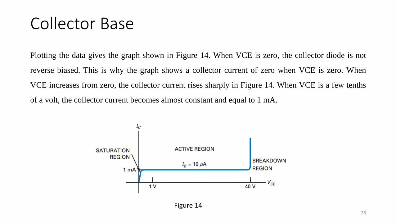
Plotting the data gives the graph shown in Figure 14. When VCE is zero, the collector diode is not
reverse biased. This is why the graph shows a collector current of zero when VCE is zero. When
VCE increases from zero, the collector current rises sharply in Figure 14. When VCE is a few tenths
of a volt, the collector current becomes almost constant and equal to 1 mA.
Figure 1426

Collector Base
• After the collector diode becomes reverse biased, it is gathering all the electrons that reach its depletion
layer.
• Further increases in VCE cannot increase the collector current. This is because the collector can collect
only those free electrons that the emitter injects into the base. The number of these injected electrons
depends only on the base circuit, not on the collector circuit. This is why Figure 14 shows a constant
collector current between a VCE of less than 1 V to a VCE of more than 40 V.
• If VCE is greater than 40 V, the collector diode breaks down and normal transistor action is lost. The
transistor is not intended to operate in the breakdown region. For this reason, one of the maximum
ratings to look for on a transistor data sheet is the collector-emitter breakdown voltage VCE(max). If the
transistor breaks down, it will be destroyed.
27

Collector Voltage and Power
• Kirchhoff’s voltage law says that the sum of voltages around a loop or closed path is equal to zero.
• When applied to the collector circuit of Figure 13, Kirchhoff’s voltage law gives us this derivation:
VCE = VCC - ICRC
• This says that the collector-emitter voltage equals the collector supply voltage minus the voltage
across the collector resistor.
• In Figure 13, the transistor has a power dissipation of approximately: PD = VCE * IC.
• This says that the transistor power equals the collector-emitter voltage times the collector current.
This power dissipation causes the junction temperature of the collector diode to increase. The
higher the power, the higher the junction temperature.
28

Collector Voltage and Power
Transistors will burn out when the junction temperature is between 150 and 200°C.
One of the most important pieces of information on a data sheet is the maximum
power rating PD(max). The power dissipation given by the previous equation must
be less than PD(max). Otherwise, the transistor will be destroyed.
29
Regions of Operation
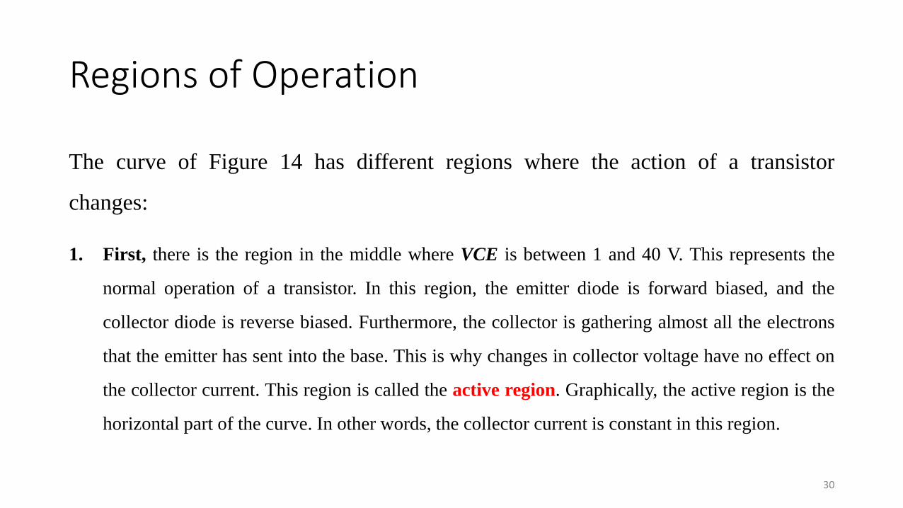
The curve of Figure 14 has different regions where the action of a transistor
changes:
1. First, there is the region in the middle where VCE is between 1 and 40 V. This represents the
normal operation of a transistor. In this region, the emitter diode is forward biased, and the
collector diode is reverse biased. Furthermore, the collector is gathering almost all the electrons
that the emitter has sent into the base. This is why changes in collector voltage have no effect on
the collector current. This region is called the active region. Graphically, the active region is the
horizontal part of the curve. In other words, the collector current is constant in this region.
30

Regions of Operation
2. Another region of operation is the breakdown region. The transistor should never operate in
this region because it will be destroyed. Unlike the zener diode, which is optimized for
breakdown operation, a transistor is not intended for operation in the breakdown region.
3. Third region, there is the early rising part of the curve, where VCE is between 0 V and a few
tenths of a volt. This sloping part of the curve is called the saturation region. In this region, the
collector diode has insufficient positive voltage to collect all the free electrons injected into the
base. In this region, the base current IB is larger than normal and the current gain dc is smaller
than normal.
31

More Curves
If we measure IC and VCE for IB = 20 A, we can plot the second curve of Figure 15. The curve is
similar to the first curve, except that the collector current is 2 mA in the active region. Again, the
collector current is constant in the active region. When we plot several curves for different base
currents, we get a set of collector curves like those in Figure 15.
Another way to get this set of curves is with a curve tracer (a test instrument that can display IC
versus VCE for a transistor). In the active region of Figure 15, each collector current is 100 times
greater than the corresponding base current. For instance, the top curve has a collector current of 7
mA and a base current of 70 A. This gives a current gain of:
32

More Curves
If you check any other curve, you get the same result:
a current gain of 100. With other transistors, the
current gain may be different from 100, but the shape
of the curves will be similar. All transistors have an
active region, a saturation region, and a breakdown
region. The active region is the most important
because amplification (enlargement) of signals is
possible in the active region.
Figure 15
33
Cut-off Region
• Figure 15 has an unexpected curve, the one on the bottom. This represents a fourth possible
region of operation. Notice that the base current is zero, but there still is a small collector current.
On a curve tracer, this current is usually so small that you cannot see it. This bottom curve is called
the cutoff region of the transistor, and the small collector current is called the collector cutoff
current.
• The collector cutoff current exist, because the collector diode has reverse minority-carrier current
and surface-leakage current. In a well- designed circuit, the collector cutoff current is small enough
to ignore. For instance, a 2N3904 has a collector cutoff current of 50 nA. If the actual collector
current is 1 mA, ignoring a collector cutoff current of 50 nA produces a calculation error of less
than 5 percent. 34
RECAP
• As we discussed earlier, the transistor has four distinct operating regions: active,
cutoff, saturation, and breakdown.
• Transistors operate in the active region when they are used to amplify weak
signals. Sometimes, the active region is called the linear region because changes
in the input signal produce proportional changes in the output signal.
• The saturation and cutoff regions are useful in digital and computer circuits,
referred to as switching circuits.
35

Transistor Approximation
• Figure 16 (a) shows a transistor. A voltage VBE appears across the emitter diode, and a
voltage VCE appears across the collector-emitter terminals. What is the equivalent circuit
for this transistor?
• The equivalent circuit for this transistor is shown in Figure 16 (b) shows the second
approximation of a transistor, by using use the approximation of a diode when calculating
base current. For silicon transistors, this means that VBE = 0.7 V. (For germanium
transistors, VBE = 0.3 V) and the base and collector currents will be slightly less than
their ideal values.
36

Transistor Equivalent Circuit
(a) (b)
Figure 16
37

Example 1
The transistor of the figure below has βdc = 300. Calculate IB, IC, VCE, and PD.
38

Example 2
What is the collector-emitter voltage in the figure below?
39

Example 3
What is the collector-emitter voltage in the three preceding examples if the base
supply voltage is 5 V?
40

References:
1. Albert P. Malvino and David J. Bates, 2015, Electronic Principles, Publisher:
McGraw-Hill Education, 8th edition.
2. Thomas L. Floyed, 2012, Electronic Devices: Electron Flow Version, 9th
edition, https://hristotrifonov.files.wordpress.com/2012/10/electronic-devices-
9th-edition-by-floyd.pdf .
41
Related Documents