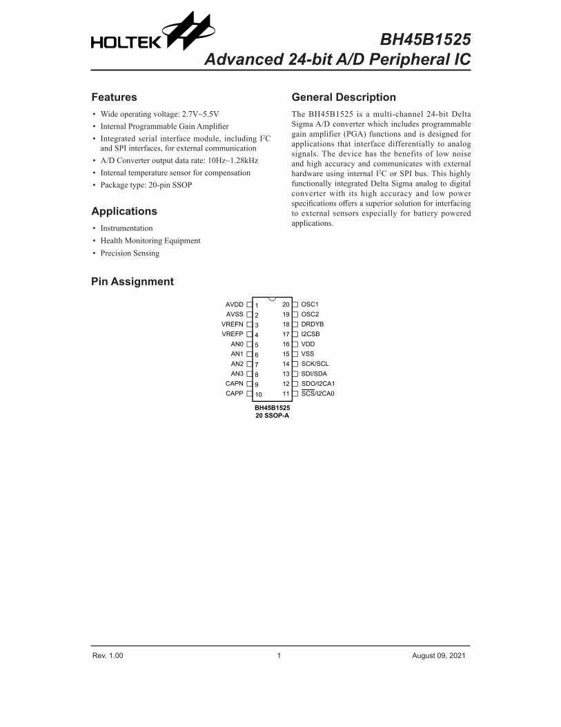
Rev. 1.00 1 August 09, 2021 BH45B1525 Advanced 24-bit A/D Peripheral IC Pin Assignment 20 19 18 17 16 15 14 13 12 11 1 2 3 4 5 6 7 8 9 10 OSC1 OSC2 AN3 CAPN CAPP SCS/I2CA0 SDO/I2CA1 DRDYB VREFN AN1 VREFP AN0 AN2 I2CSB SDI/SDA SCK/SCL VSS VDD AVSS AVDD BH45B1525 20 SSOP-A Features • Wide operating voltage: 2.7V~5.5V • Internal Programmable Gain Amplifier • Integrated serial interface module, including I 2 C and SPI interfaces, for external communication • A/D Converter output data rate: 10Hz~1.28kHz • Internal temperature sensor for compensation • Package type: 20-pin SSOP Applications • Instrumentation • Health Monitoring Equipment • Precision Sensing General Description The BH45B1525 is a multi-channel 24-bit Delta Sigma A/D converter which includes programmable gain amplifier (PGA) functions and is designed for applications that interface differentially to analog signals. The device has the benefits of low noise and high accuracy and communicates with external hardware using internal I 2 C or SPI bus. This highly functionally integrated Delta Sigma analog to digital converter with its high accuracy and low power specifications offers a superior solution for interfacing to external sensors especially for battery powered applications.

Welcome message from author
This document is posted to help you gain knowledge. Please leave a comment to let me know what you think about it! Share it to your friends and learn new things together.
Transcript
Rev. 1.00 1 August 09, 2021 Rev. 1.00 PB August 09, 2021
BH45B1525
Advanced 24-bit A/D Peripheral IC
Pin Assignment
20191817161514131211
12345678910
OSC1OSC2
AN3CAPNCAPP SCS/I2CA0
SDO/I2CA1
DRDYBVREFN
AN1
VREFPAN0
AN2
I2CSB
SDI/SDASCK/SCLVSSVDD
AVSSAVDD
BH45B152520 SSOP-A
Features• Wide operating voltage: 2.7V~5.5V• Internal Programmable Gain Amplifier• Integrated serial interface module, including I2C
and SPI interfaces, for external communication• A/D Converter output data rate: 10Hz~1.28kHz• Internal temperature sensor for compensation• Package type: 20-pin SSOP
Applications• Instrumentation• Health Monitoring Equipment• Precision Sensing
General DescriptionThe BH45B1525 is a multi-channel 24-bit Delta Sigma A/D converter which includes programmable gain amplifier (PGA) functions and is designed for applications that interface differentially to analog signals. The device has the benefits of low noise and high accuracy and communicates with external hardware using internal I2C or SPI bus. This highly functionally integrated Delta Sigma analog to digital converter with its high accuracy and low power specifications offers a superior solution for interfacing to external sensors especially for battery powered applications.
Rev. 1.00 2 August 09, 2021
BH45B1525
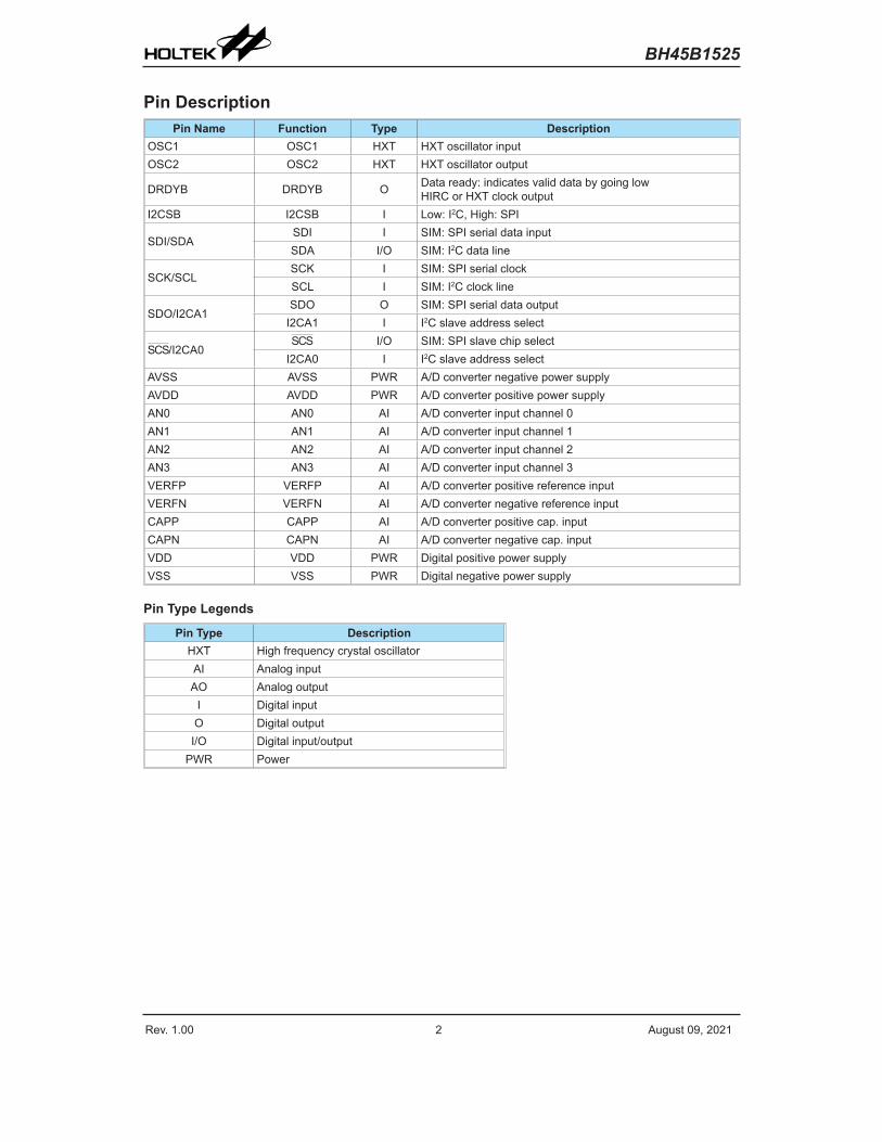
Pin DescriptionPin Name Function Type Description
OSC1 OSC1 HXT HXT oscillator inputOSC2 OSC2 HXT HXT oscillator output
DRDYB DRDYB O Data ready: indicates valid data by going lowHIRC or HXT clock output
I2CSB I2CSB I Low: I2C, High: SPI
SDI/SDASDI I SIM: SPI serial data inputSDA I/O SIM: I2C data line
SCK/SCLSCK I SIM: SPI serial clockSCL I SIM: I2C clock line
SDO/I2CA1SDO O SIM: SPI serial data output
I2CA1 I I2C slave address select
SCS/I2CA0SCS I/O SIM: SPI slave chip select
I2CA0 I I2C slave address selectAVSS AVSS PWR A/D converter negative power supplyAVDD AVDD PWR A/D converter positive power supplyAN0 AN0 AI A/D converter input channel 0AN1 AN1 AI A/D converter input channel 1AN2 AN2 AI A/D converter input channel 2AN3 AN3 AI A/D converter input channel 3VERFP VERFP AI A/D converter positive reference inputVERFN VERFN AI A/D converter negative reference inputCAPP CAPP AI A/D converter positive cap. inputCAPN CAPN AI A/D converter negative cap. inputVDD VDD PWR Digital positive power supplyVSS VSS PWR Digital negative power supply
Pin Type Legends
Pin Type DescriptionHXT High frequency crystal oscillatorAI Analog inputAO Analog output
I Digital inputO Digital outputI/O Digital input/output
PWR Power
Rev. 1.00 3 August 09, 2021
BH45B1525
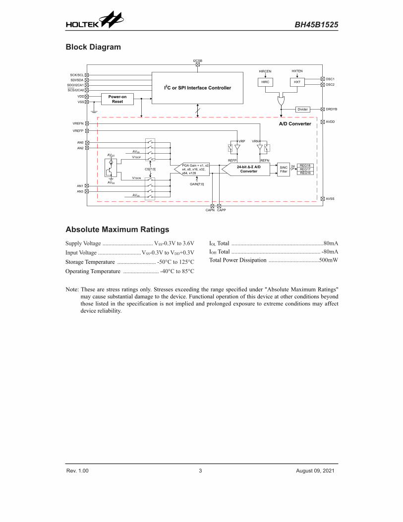
Block Diagram
SCK/SCL
VREFN
VREFP
VRP VRN
REFNREFP
24-bit Δ-Σ A/D Converter
PGA Gain = x1, x2,x4, x8, x16, x32,x64, x128
SINCFilterCS[7:0]
VTSOP
GAIN[7:0]
REG18REG17REG16
AN2
AVDD
AVSS
AN0
AN1
AN3AVSS
CAPN CAPP
OSC1
OSC2HIRC
I2CSB
VDD
24
AVSS
VTSON
DRDYB
I2C or SPI Interface ControllerSDI/SDA
SDO/I2CA1SCS/I2CA0
VSSPower-on
Reset
A/D Converter
AVDD
AVSS
HXT
HIRCEN HXTEN
Divider
Absolute Maximum RatingsSupply Voltage .................................. VSS-0.3V to 3.6VInput Voltage .............................VSS-0.3V to VDD+0.3VStorage Temperature .......................... -50°C to 125°COperating Temperature ........................ -40°C to 85°C
IOL Total ..............................................................80mA IOH Total ............................................................ -80mA Total Power Dissipation ..................................500mW
Note: These are stress ratings only. Stresses exceeding the range specified under "Absolute Maximum Ratings" may cause substantial damage to the device. Functional operation of this device at other conditions beyond those listed in the specification is not implied and prolonged exposure to extreme conditions may affect device reliability.
Rev. 1.00 4 August 09, 2021
BH45B1525
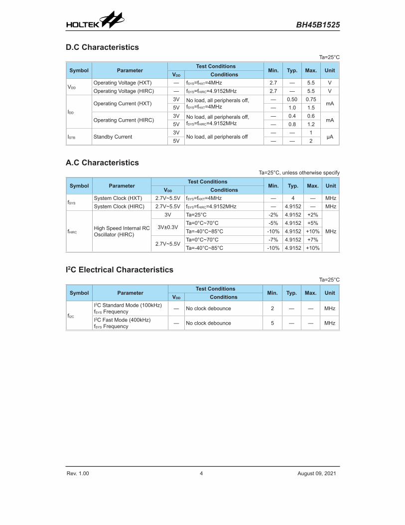
D.C CharacteristicsTa=25°C
Symbol ParameterTest Conditions
Min. Typ. Max. UnitVDD Conditions
VDDOperating Voltage (HXT) — fSYS=fHXT=4MHz 2.7 — 5.5 VOperating Voltage (HIRC) — fSYS=fHIRC=4.9152MHz 2.7 — 5.5 V
IDD
Operating Current (HXT)3V No load, all peripherals off,
fSYS=fHXT=4MHz— 0.50 0.75
mA5V — 1.0 1.5
Operating Current (HIRC)3V No load, all peripherals off,
fSYS=fHIRC=4.9152MHz— 0.4 0.6
mA5V — 0.8 1.2
ISTB Standby Current3V
No load, all peripherals off— — 1
μA5V — — 2
A.C CharacteristicsTa=25°C, unless otherwise specify
Symbol ParameterTest Conditions
Min. Typ. Max. UnitVDD Conditions
fSYSSystem Clock (HXT) 2.7V~5.5V fSYS=fHXT=4MHz — 4 — MHzSystem Clock (HIRC) 2.7V~5.5V fSYS=fHIRC=4.9152MHz — 4.9152 — MHz
fHIRCHigh Speed Internal RC Oscillator (HIRC)
3V Ta=25°C -2% 4.9152 +2%
MHz3V±0.3V
Ta=0°C~70°C -5% 4.9152 +5%Ta=-40°C~85°C -10% 4.9152 +10%
2.7V~5.5VTa=0°C~70°C -7% 4.9152 +7%Ta=-40°C~85°C -10% 4.9152 +10%
I2C Electrical CharacteristicsTa=25°C
Symbol ParameterTest Conditions
Min. Typ. Max. UnitVDD Conditions
fI2C
I2C Standard Mode (100kHz)fSYS Frequency — No clock debounce 2 — — MHz
I2C Fast Mode (400kHz)fSYS Frequency — No clock debounce 5 — — MHz
Rev. 1.00 5 August 09, 2021
BH45B1525
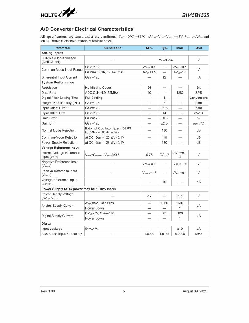
A/D Converter Electrical CharacteristicsAll specifications are tested under the conditions: Ta=-40°C~+85°C, AVDD=VDD=VREFP=+5V, VREFN=AVSS and VREF Buffer is disabled, unless otherwise noted.
Parameter Conditions Min. Typ. Max. UnitAnalog InputsFull-Scale Input Voltage(AINP-AINN) — ±VREF/Gain V
Common-Mode Input RangeGain=1, 2 AVSS-0.1 — AVDD+0.1
VGain=4, 8, 16, 32, 64, 128 AVSS+1.5 — AVDD-1.5
Differential Input Current Gain=128 — ±2 — nASystem PerformanceResolution No Missing Codes 24 — — BitData Rate ADC CLK=4.9152MHz 10 — 1280 SPSDigital Filter Settling Time Full Settling — 4 — ConversionsIntegral Non-linearity (INL) Gain=128 — 7 — ppmInput Offset Error Gain=128 — ±1.6 — ppmInput Offset Drift Gain=128 — ±4 — nV/°CGain Error Gain=128 — ±0.3 — %Gain Drift Gain=128 — ±2.5 — ppm/°C
Normal Mode Rejection External Oscillator, fDATA=10SPSfin=50Hz or 60Hz, ±1Hz — 130 — dB
Common-Mode Rejection at DC, Gain=128, ΔV=0.1V — 110 — dBPower-Supply Rejection at DC, Gain=128, ΔV=0.1V — 120 — dBVoltage Reference InputInternal Voltage Reference Input (VREF) VREF=(VREFP - VREFN)×0.5 0.75 AVDD/2 (AVDD+0.1)
/2 V
Negative Reference Input (VREFN) — AVSS-0.1 — VREFP-1.5 V
Positive Reference Input (VREFP) — VREFN+1.5 — AVDD+0.1 V
Voltage Reference Input Current — — 10 — nA
Power Supply (ADC power may be 5~10% more)Power Supply Voltage (AVDD, VDD) — 2.7 — 5.5 V
Analog Supply CurrentAVDD=5V, Gain=128 — 1350 2500
μAPower Down — — 1
Digital Supply CurrentDVDD=5V, Gain=128 — 75 120
μAPower Down — — 1
DigitalInput Leakage 0<VIN<VDD — — ±10 μAADC Clock Input Frequency — 1.0000 4.9152 6.0000 MHz
Rev. 1.00 6 August 09, 2021
BH45B1525
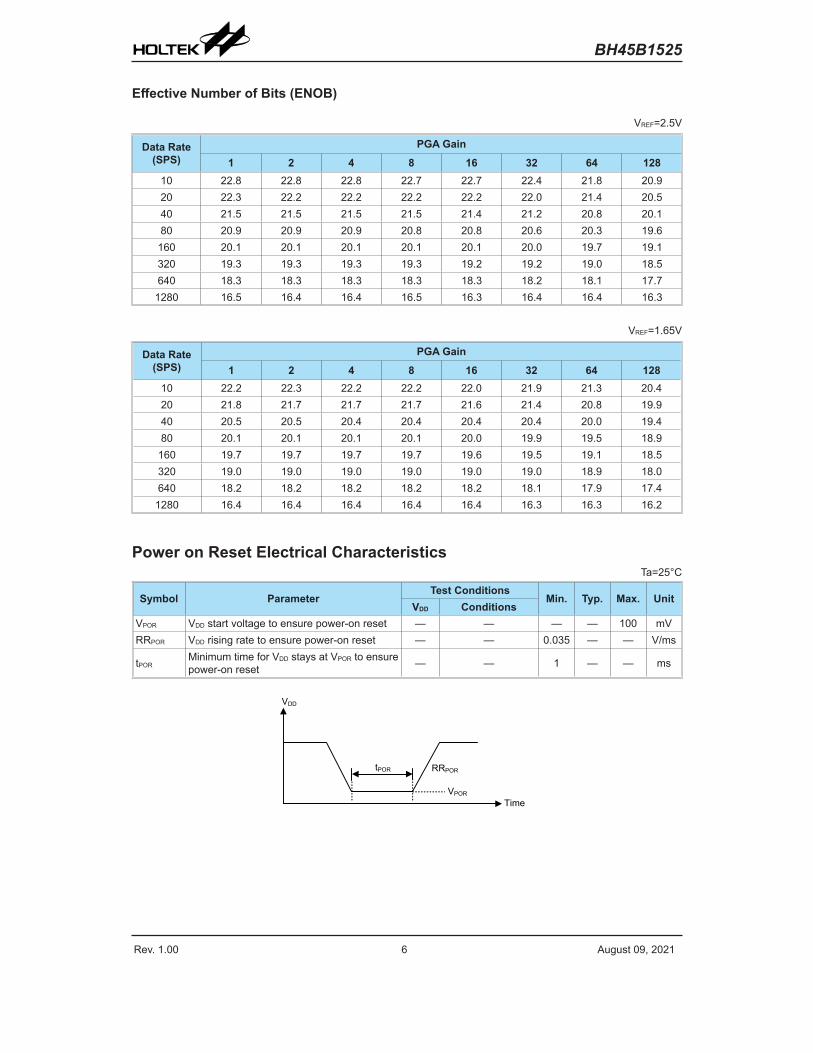
Effective Number of Bits (ENOB)
VREF=2.5V
Data Rate (SPS)
PGA Gain1 2 4 8 16 32 64 128
10 22.8 22.8 22.8 22.7 22.7 22.4 21.8 20.920 22.3 22.2 22.2 22.2 22.2 22.0 21.4 20.540 21.5 21.5 21.5 21.5 21.4 21.2 20.8 20.180 20.9 20.9 20.9 20.8 20.8 20.6 20.3 19.6160 20.1 20.1 20.1 20.1 20.1 20.0 19.7 19.1320 19.3 19.3 19.3 19.3 19.2 19.2 19.0 18.5640 18.3 18.3 18.3 18.3 18.3 18.2 18.1 17.71280 16.5 16.4 16.4 16.5 16.3 16.4 16.4 16.3
VREF=1.65V
Data Rate (SPS)
PGA Gain1 2 4 8 16 32 64 128
10 22.2 22.3 22.2 22.2 22.0 21.9 21.3 20.420 21.8 21.7 21.7 21.7 21.6 21.4 20.8 19.940 20.5 20.5 20.4 20.4 20.4 20.4 20.0 19.480 20.1 20.1 20.1 20.1 20.0 19.9 19.5 18.9160 19.7 19.7 19.7 19.7 19.6 19.5 19.1 18.5320 19.0 19.0 19.0 19.0 19.0 19.0 18.9 18.0640 18.2 18.2 18.2 18.2 18.2 18.1 17.9 17.41280 16.4 16.4 16.4 16.4 16.4 16.3 16.3 16.2
Power on Reset Electrical CharacteristicsTa=25°C
Symbol ParameterTest Conditions
Min. Typ. Max. UnitVDD Conditions
VPOR VDD start voltage to ensure power-on reset — — — — 100 mVRRPOR VDD rising rate to ensure power-on reset — — 0.035 — — V/ms
tPORMinimum time for VDD stays at VPOR to ensure power-on reset — — 1 — — ms
VDD
tPOR RRPOR
VPOR
Time
Rev. 1.00 7 August 09, 2021
BH45B1525
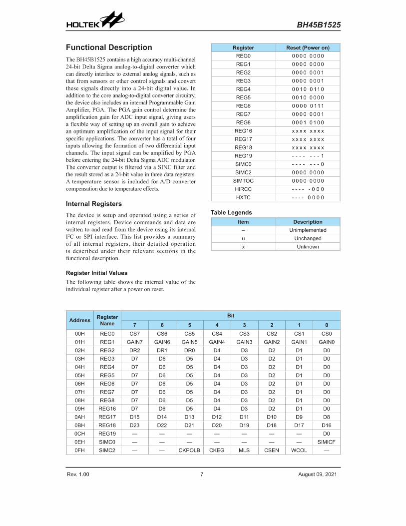
Address Register Name
Bit7 6 5 4 3 2 1 0
00H REG0 CS7 CS6 CS5 CS4 CS3 CS2 CS1 CS001H REG1 GAIN7 GAIN6 GAIN5 GAIN4 GAIN3 GAIN2 GAIN1 GAIN002H REG2 DR2 DR1 DR0 D4 D3 D2 D1 D003H REG3 D7 D6 D5 D4 D3 D2 D1 D004H REG4 D7 D6 D5 D4 D3 D2 D1 D005H REG5 D7 D6 D5 D4 D3 D2 D1 D006H REG6 D7 D6 D5 D4 D3 D2 D1 D007H REG7 D7 D6 D5 D4 D3 D2 D1 D008H REG8 D7 D6 D5 D4 D3 D2 D1 D009H REG16 D7 D6 D5 D4 D3 D2 D1 D00AH REG17 D15 D14 D13 D12 D11 D10 D9 D80BH REG18 D23 D22 D21 D20 D19 D18 D17 D160CH REG19 — — — — — — — D00EH SIMC0 — — — — — — — SIMICF0FH SIMC2 — — CKPOLB CKEG MLS CSEN WCOL —
Functional DescriptionThe BH45B1525 contains a high accuracy multi-channel 24-bit Delta Sigma analog-to-digital converter which can directly interface to external analog signals, such as that from sensors or other control signals and convert these signals directly into a 24-bit digital value. In addition to the core analog-to-digital converter circuitry, the device also includes an internal Programmable Gain Amplifier, PGA. The PGA gain control determine the amplification gain for ADC input signal, giving users a flexible way of setting up an overall gain to achieve an optimum amplification of the input signal for their specific applications. The converter has a total of four inputs allowing the formation of two differential input channels. The input signal can be amplified by PGA before entering the 24-bit Delta Sigma ADC modulator. The converter output is filtered via a SINC filter and the result stored as a 24-bit value in three data registers. A temperature sensor is included for A/D converter compensation due to temperature effects.
Internal RegistersThe device is setup and operated using a series of internal registers. Device commands and data are written to and read from the device using its internal I2C or SPI interface. This list provides a summary of all internal registers, their detailed operation is described under their relevant sections in the functional description.
Register Initial ValuesThe following table shows the internal value of the individual register after a power on reset.
Register Reset (Power on)REG0 0 0 0 0 0 0 0 0REG1 0 0 0 0 0 0 0 0REG2 0 0 0 0 0 0 0 1REG3 0 0 0 0 0 0 0 1REG4 0 0 1 0 0 11 0REG5 0 0 1 0 0 0 0 0REG6 0 0 0 0 0 111REG7 0 0 0 0 0 0 0 1REG8 0 0 0 1 0 1 0 0REG16 x x x x x x x xREG17 x x x x x x x xREG18 x x x x x x x xREG19 - - - - - - - 1SIMC0 - - - - - - - 0SIMC2 0 0 0 0 0 0 0 0
SIMTOC 0 0 0 0 0 0 0 0HIRCC - - - - - 0 0 0HXTC - - - - 0 0 0 0
Table LegendsItem Description
– Unimplementedu Unchangedx Unknown
Rev. 1.00 8 August 09, 2021
BH45B1525
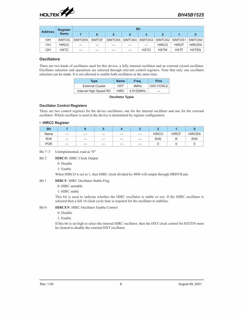
Address Register Name
Bit7 6 5 4 3 2 1 0
10H SIMTOC SIMTOEN SIMTOF SIMTOS5 SIMTOS4 SIMTOS3 SIMTOS2 SIMTOS1 SIMTOS011H HIRCC — — — — — HIRCO HIRCF HIRCEN12H HXTC — — — — HXTO HXTM HXTF HXTEN
OscillatorsThere are two kinds of oscillators used for this device, a fully internal oscillator and an external crystal oscillator. Oscillator selection and operations are selected through relevant control registers. Note that only one oscillator selection can be made. It is not allowed to enable both oscillators at the same time.
Type Name Freq. PinsExternal Crystal HXT 4MHz OSC1/OSC2
Internal High Speed RC HIRC 4.9152MHz —
Oscillator Types
Oscillator Control RegistersThere are two control registers for the device oscillators, one for the internal oscillator and one for the external oscillator. Which oscillator is used in the device is determined by register configuration.
• HIRCC RegisterBit 7 6 5 4 3 2 1 0
Name — — — — — HIRCO HIRCF HIRCENR/W — — — — — R/W R R/WPOR — — — — — 0 0 0
Bit 7~3 Unimplemented, read as "0"
Bit 2 HIRCO: HIRC Clock Output0: Disable1: Enable
When HIRCO is set to 1, then HIRC clock divided by 4096 will output through DRDYB pin.
Bit 1 HIRCF: HIRC Oscillator Stable Flag0: HIRC unstable1: HIRC stable
This bit is used to indicate whether the HIRC oscillator is stable or not. If the HIRC oscillator is selected then a full 16 clock cycle time is required for the oscillator to stabilise.
Bit 0 HIRCEN: HIRC Oscillator Enable Control0: Disable1: Enable
If this bit is set high to select the internal HIRC oscillator, then the HXT clock control bit HXTEN must be cleared to disable the external HXT oscillator.
Rev. 1.00 9 August 09, 2021
BH45B1525
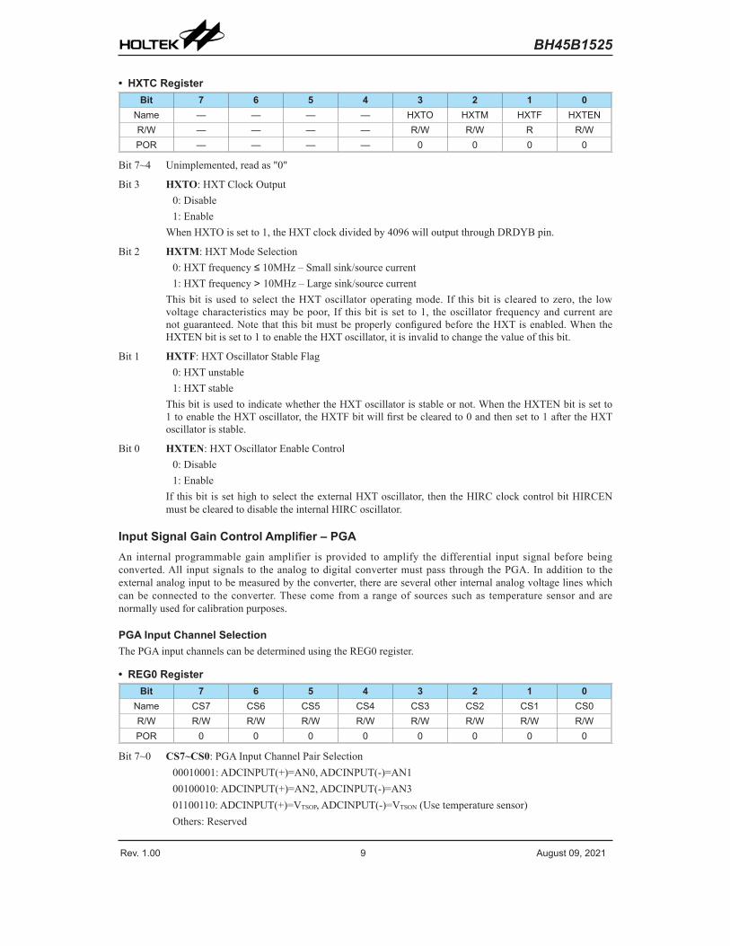
• HXTC RegisterBit 7 6 5 4 3 2 1 0
Name — — — — HXTO HXTM HXTF HXTENR/W — — — — R/W R/W R R/WPOR — — — — 0 0 0 0
Bit 7~4 Unimplemented, read as "0"
Bit 3 HXTO: HXT Clock Output0: Disable1: Enable
When HXTO is set to 1, the HXT clock divided by 4096 will output through DRDYB pin.
Bit 2 HXTM: HXT Mode Selection0: HXT frequency ≤ 10MHz – Small sink/source current1: HXT frequency > 10MHz – Large sink/source current
This bit is used to select the HXT oscillator operating mode. If this bit is cleared to zero, the low voltage characteristics may be poor, If this bit is set to 1, the oscillator frequency and current are not guaranteed. Note that this bit must be properly configured before the HXT is enabled. When the HXTEN bit is set to 1 to enable the HXT oscillator, it is invalid to change the value of this bit.
Bit 1 HXTF: HXT Oscillator Stable Flag0: HXT unstable1: HXT stable
This bit is used to indicate whether the HXT oscillator is stable or not. When the HXTEN bit is set to 1 to enable the HXT oscillator, the HXTF bit will first be cleared to 0 and then set to 1 after the HXT oscillator is stable.
Bit 0 HXTEN: HXT Oscillator Enable Control0: Disable1: Enable
If this bit is set high to select the external HXT oscillator, then the HIRC clock control bit HIRCEN must be cleared to disable the internal HIRC oscillator.
Input Signal Gain Control Amplifier – PGAAn internal programmable gain amplifier is provided to amplify the differential input signal before being converted. All input signals to the analog to digital converter must pass through the PGA. In addition to the external analog input to be measured by the converter, there are several other internal analog voltage lines which can be connected to the converter. These come from a range of sources such as temperature sensor and are normally used for calibration purposes.
PGA Input Channel SelectionThe PGA input channels can be determined using the REG0 register.
• REG0 RegisterBit 7 6 5 4 3 2 1 0
Name CS7 CS6 CS5 CS4 CS3 CS2 CS1 CS0R/W R/W R/W R/W R/W R/W R/W R/W R/WPOR 0 0 0 0 0 0 0 0
Bit 7~0 CS7~CS0: PGA Input Channel Pair Selection00010001: ADCINPUT(+)=AN0, ADCINPUT(-)=AN100100010: ADCINPUT(+)=AN2, ADCINPUT(-)=AN301100110: ADCINPUT(+)=VTSOP, ADCINPUT(-)=VTSON (Use temperature sensor)Others: Reserved
Rev. 1.00 10 August 09, 2021
BH45B1525
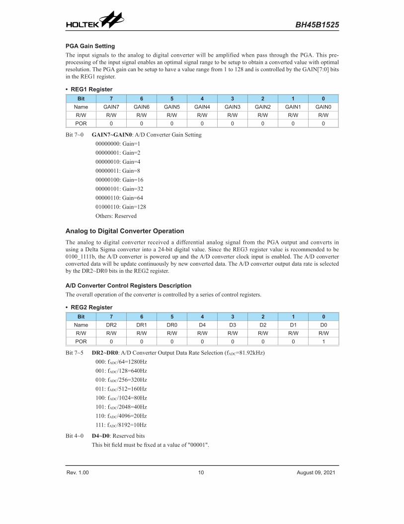
PGA Gain SettingThe input signals to the analog to digital converter will be amplified when pass through the PGA. This pre-processing of the input signal enables an optimal signal range to be setup to obtain a converted value with optimal resolution. The PGA gain can be setup to have a value range from 1 to 128 and is controlled by the GAIN[7:0] bits in the REG1 register.
• REG1 RegisterBit 7 6 5 4 3 2 1 0
Name GAIN7 GAIN6 GAIN5 GAIN4 GAIN3 GAIN2 GAIN1 GAIN0R/W R/W R/W R/W R/W R/W R/W R/W R/WPOR 0 0 0 0 0 0 0 0
Bit 7~0 GAIN7~GAIN0: A/D Converter Gain Setting00000000: Gain=100000001: Gain=200000010: Gain=400000011: Gain=800000100: Gain=1600000101: Gain=3200000110: Gain=6401000110: Gain=128Others: Reserved
Analog to Digital Converter OperationThe analog to digital converter received a differential analog signal from the PGA output and converts in using a Delta Sigma converter into a 24-bit digital value. Since the REG3 register value is recommended to be 0100_1111b, the A/D converter is powered up and the A/D converter clock input is enabled. The A/D converter converted data will be update continuously by new converted data. The A/D converter output data rate is selected by the DR2~DR0 bits in the REG2 register.
A/D Converter Control Registers DescriptionThe overall operation of the converter is controlled by a series of control registers.
• REG2 RegisterBit 7 6 5 4 3 2 1 0
Name DR2 DR1 DR0 D4 D3 D2 D1 D0R/W R/W R/W R/W R/W R/W R/W R/W R/WPOR 0 0 0 0 0 0 0 1
Bit 7~5 DR2~DR0: A/D Converter Output Data Rate Selection (fADC=81.92kHz)000: fADC/64=1280Hz001: fADC/128=640Hz010: fADC/256=320Hz011: fADC/512=160Hz100: fADC/1024=80Hz101: fADC/2048=40Hz110: fADC/4096=20Hz111: fADC/8192=10Hz
Bit 4~0 D4~D0: Reserved bitsThis bit field must be fixed at a value of "00001".
Rev. 1.00 11 August 09, 2021
BH45B1525
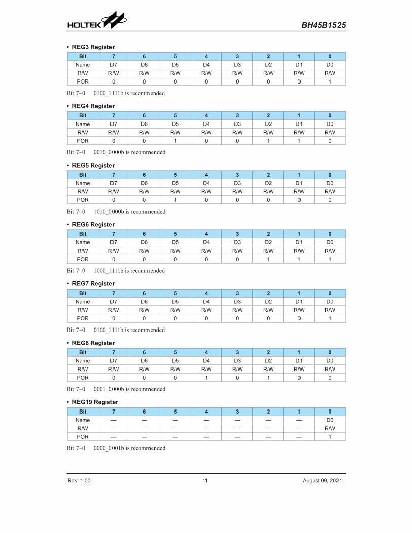
• REG3 RegisterBit 7 6 5 4 3 2 1 0
Name D7 D6 D5 D4 D3 D2 D1 D0R/W R/W R/W R/W R/W R/W R/W R/W R/WPOR 0 0 0 0 0 0 0 1
Bit 7~0 0100_1111b is recommended
• REG4 RegisterBit 7 6 5 4 3 2 1 0
Name D7 D6 D5 D4 D3 D2 D1 D0R/W R/W R/W R/W R/W R/W R/W R/W R/WPOR 0 0 1 0 0 1 1 0
Bit 7~0 0010_0000b is recommended
• REG5 RegisterBit 7 6 5 4 3 2 1 0
Name D7 D6 D5 D4 D3 D2 D1 D0R/W R/W R/W R/W R/W R/W R/W R/W R/WPOR 0 0 1 0 0 0 0 0
Bit 7~0 1010_0000b is recommended
• REG6 RegisterBit 7 6 5 4 3 2 1 0
Name D7 D6 D5 D4 D3 D2 D1 D0R/W R/W R/W R/W R/W R/W R/W R/W R/WPOR 0 0 0 0 0 1 1 1
Bit 7~0 1000_1111b is recommended
• REG7 RegisterBit 7 6 5 4 3 2 1 0
Name D7 D6 D5 D4 D3 D2 D1 D0R/W R/W R/W R/W R/W R/W R/W R/W R/WPOR 0 0 0 0 0 0 0 1
Bit 7~0 0100_1111b is recommended
• REG8 RegisterBit 7 6 5 4 3 2 1 0
Name D7 D6 D5 D4 D3 D2 D1 D0R/W R/W R/W R/W R/W R/W R/W R/W R/WPOR 0 0 0 1 0 1 0 0
Bit 7~0 0001_0000b is recommended
• REG19 RegisterBit 7 6 5 4 3 2 1 0
Name — — — — — — — D0R/W — — — — — — — R/WPOR — — — — — — — 1
Bit 7~0 0000_0001b is recommended
Rev. 1.00 12 August 09, 2021
BH45B1525
A/D Converterd Reference VoltageThe differential reference voltage supply to the A/D Converter can be supplied from an external reference source supplied on pins VREFP and VREFN.
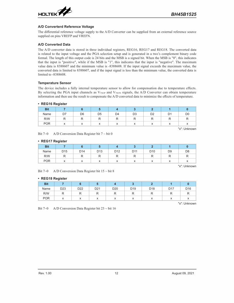
A/D Converted DataThe A/D converter data is stored in three individual registers, REG16, REG17 and REG18. The converted data is related to the input voltage and the PGA selection setup and is generated in a two’s complement binary code formal. The length of this output code is 24 bits and the MSB is a signed bit. When the MSB is "0", this indicates that the input is "positive", while if the MSB is "1", this indicates that the input is "negative". The maximum value data is 8388607 and the minimum value is -8388608. If the input signal exceeds the maximum value, the converted data is limited to 8388607, and if the input signal is less than the minimum value, the converted data is limited to -8388608.
Temperature SensorThe device includes a fully internal temperature sensor to allow for compensation due to temperature effects. By selecting the PGA input channels as VTSOP and VTSON signals, the A/D Converter can obtain temperature information and then use the result to compensate the A/D converted data to minimize the effects of temperature.
• REG16 RegisterBit 7 6 5 4 3 2 1 0
Name D7 D6 D5 D4 D3 D2 D1 D0R/W R R R R R R R RPOR x x x x x x x x
"x": UnknownBit 7~0 A/D Conversion Data Register bit 7 ~ bit 0
• REG17 RegisterBit 7 6 5 4 3 2 1 0
Name D15 D14 D13 D12 D11 D10 D9 D8R/W R R R R R R R RPOR x x x x x x x x
"x": UnknownBit 7~0 A/D Conversion Data Register bit 15 ~ bit 8
• REG18 RegisterBit 7 6 5 4 3 2 1 0
Name D23 D22 D21 D20 D19 D18 D17 D16R/W R R R R R R R RPOR x x x x x x x x
"x": UnknownBit 7~0 A/D Conversion Data Register bit 23 ~ bit 16
Rev. 1.00 13 August 09, 2021
BH45B1525
External Interface CommunicationThe device contains a Serial Interface Module, which includes I2C and SPI interfaces, to allow an easy method of communication with external peripheral hardware. The SIM function is always enabled. As both interface types share the same pins and registers, the choice of whether the SPI or I2C type is used is made using the I2CSB pin. Note that after the power on reset, the I2CSB pin is low.
I2CSB I2C/SPI SDI/SDA
SCK/SCL
SDO/I2CA1
SCS/I2CA0
0 I2C SDA SCL I2CA1 I2CA01 SPI SDI SCK SDO SCS
I2C Serial InterfaceThe device will communicate with external hardware using its internal I2C interface if the I2CSB pin is low. Originally developed by Philips, the I2C interface is a two line low speed serial interface for bidirectional synchronous serial data transfer between different ICs or modules. With the advantage of only two lines for communication, a relatively simple communication protocol and the ability to accommodate multiple devices on the same bus has made it an extremely popular interfaces type for many applications.
I2C OperationThe I2C serial interface is a two line interface, a serial data line, SDA, and a serial clock line, SCL. Both lines are connected to the positive supply via pull-up resistors. When the bus is free, both lines are high. Devices connected to the bus must have open-drain or open-collector outputs to implement a wired-or function. Data transfer is initiated only when the bus is not busy.
Note that no chip select line exists, as each device on the I2C bus is identified by a unique address which will be transmitted and received on the I2C bus. When two devices communicate with each other on the bidirectional I2C bus, one is known as the master device and one as the slave device. Both master and slave can transmit and receive data, however, it is the master device that has overall control of the bus, and it is only the master that will drive the SCL clock line. This device only operates in the slave mode, and will therefore only operate in response to the master. There are two methods for this device to transfer data on the I2C bus, the slave transmit mode and the slave receive mode.
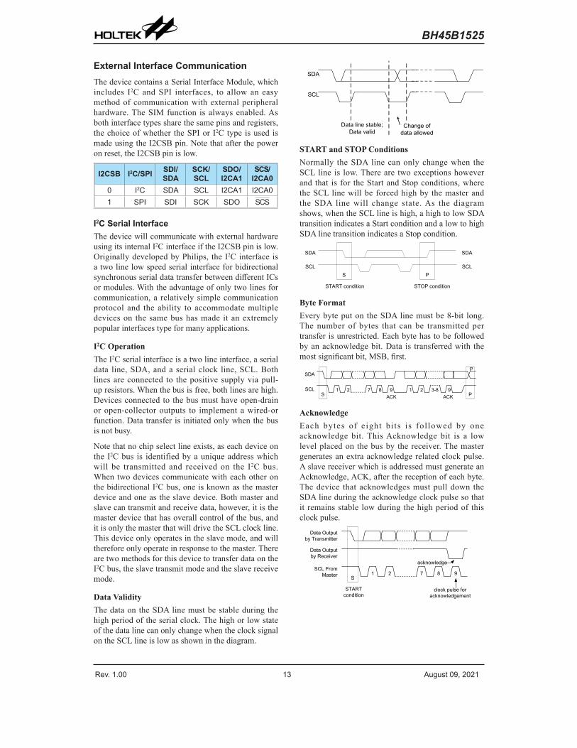
Data ValidityThe data on the SDA line must be stable during the high period of the serial clock. The high or low state of the data line can only change when the clock signal on the SCL line is low as shown in the diagram.
SDA
SCL
Data line stable;Data valid
Change of data allowed
START and STOP ConditionsNormally the SDA line can only change when the SCL line is low. There are two exceptions however and that is for the Start and Stop conditions, where the SCL line will be forced high by the master and the SDA line will change state. As the diagram shows, when the SCL line is high, a high to low SDA transition indicates a Start condition and a low to high SDA line transition indicates a Stop condition.
PS
SDA
SCL
SDA
SCL
START condition STOP condition
Byte FormatEvery byte put on the SDA line must be 8-bit long. The number of bytes that can be transmitted per transfer is unrestricted. Each byte has to be followed by an acknowledge bit. Data is transferred with the most significant bit, MSB, first.
S P
SDA
SCL 1 2 7 8 9ACK
1 2 3-8 9ACK
P
AcknowledgeEach bytes of eight bi ts is fol lowed by one acknowledge bit. This Acknowledge bit is a low level placed on the bus by the receiver. The master generates an extra acknowledge related clock pulse. A slave receiver which is addressed must generate an Acknowledge, ACK, after the reception of each byte. The device that acknowledges must pull down the SDA line during the acknowledge clock pulse so that it remains stable low during the high period of this clock pulse.
S1 2 7 8 9
clock pulse foracknowledgement
Data Outputby Transmitter
Data Outputby Receiver
SCL FromMaster
acknowledge
STARTcondition
Rev. 1.00 14 August 09, 2021
BH45B1525
Slave AddressingThe slave address byte is the first byte received following the START condition from the master device. The first seven bits of the first byte make up the slave address. The eighth bit defines a read or write operation to be performed. When the R/W bit is "1", then a read operation is selected. A "0" selects a write operation. When an address byte is sent, the device compares the first seven bits after the START condition. If they match, the device outputs an Acknowledge on the SDA line.
I2C Address SelectionAs this device only operates as a slave, and as it may be connected to a common I2C bus along with other I2C devices, it will require a specific address for it to be communicated to by the external master.
The address of the device is setup using the I2CA0 and I2CA1 pins which allows for 4 different address values. However as the I2CA0 and I2CA1 pins are shared with the SPI interface pins, their addressing function is only enabled when the I2CSB pin is low. When the I2CSB pin is high the I2CA0 and I2CA1 addressing function will be disabled. Note that only the high 7 bits of the slave address is effective.
I2CSB I2CA1 I2CA0 I2C Slave Address
0
0 0 0xA00 1 0xB01 0 0xC01 1 0xD0
I2C Interface Read/Write Operation
• I2C Interface Write OperationA single data byte write operation requires a START condition, a slave address with an R/W bit, a valid Register Address byte, a Data byte and a STOP condition.
Bit 7 6 5 4 3 2 1 0 7 6 5 4 3 2 1 0 7 6 5 4 3 2 1 0Start Device Address Write ACK Register Address ACK Register Data ACK Stop
Slave Address
ACKWrite ACK
S Device Address 0
Register Data byte
ACK
PD7 D6 D5 D4 D3 D2 D1 D0
Register Address byte
A0A1A2A3A4A5A6 D7A7
I2C Interface Single Data Byte Write Operation
• I2C Interface Read OperationIn this mode, the master reads the device data after setting the slave address. Following the R/W bit (=‘0’) is an acknowledge bit and the register address byte which is written to the internal address pointer. After the start address of the Read Operation has been configured, another START condition and the slave address transferred on the bus followed by the R/W bit (=‘1’). Then the MSB of the data which was addressed is transmitted first on the I2C bus.
Bit 7 6 5 4 3 2 1 0 7 6 5 4 3 2 1 0 7 6 5 4 3 2 1 0 7 6 5 4 3 2 1 0
Start Device Address Write ACK Register Address ACK Start Device Address Read ACK Register Data ACK Stop
WriteACK
Slave Address
S Device Address 0
Data byte
D7 D6 D5 D4 D3 D2 D1 D0
ACK
P
ACK
Slave Address
Read
S Device Address 1
ACK
Register Address byte
A0A1A2A3A4A5A6A7
I2C Interface Single Data Byte Read Operation
Rev. 1.00 15 August 09, 2021
BH45B1525
I2C Timeout FunctionThe I2C interface includes a timeout function which is controlled by a single register. This register sets the overall enable/disable function as well as the timeout value in system clock units. Determining whether the I2C bus has timed out is implemented by reading the SIMTOF bit. This bit will be automatically set high when the I2C bus times out, but needs to be cleared manually by the application program.
• SIMTOC RegisterBit 7 6 5 4 3 2 1 0
Name SIMTOEN SIMTOF SIMTOS5 SIMTOS4 SIMTOS3 SIMTOS2 SIMTOS1 SIMTOS0R/W R/W R/W R/W R/W R/W R/W R/W R/WPOR 0 0 0 0 0 0 0 0
Bit 7 SIMTOEN: I2C Time-out Control0: Disable1: Enable
Bit 6 SIMTOF: I2C Time-out Flag0: Not occurred1: Occurred
This bit is set by Time-out function and can only be cleared by the application program.
Bit 7 SIMTOS5~SIMTOS0: I2C Time-out Selection Time0: Disable1: Enable
The I2C Time-Out clock source is fSUB/32. (fSUB=fSYS/128 )The I2C Time-Out time is (SIMTOS[5:0]+1) × (32/fSUB).
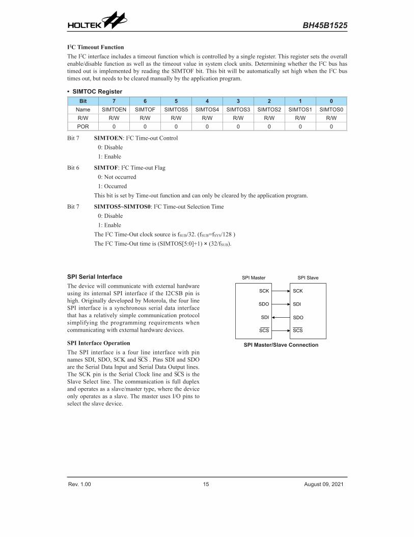
SPI Serial InterfaceThe device will communicate with external hardware using its internal SPI interface if the I2CSB pin is high. Originally developed by Motorola, the four line SPI interface is a synchronous serial data interface that has a relatively simple communication protocol simplifying the programming requirements when communicating with external hardware devices.
SPI Interface OperationThe SPI interface is a four line interface with pin names SDI, SDO, SCK and SCS . Pins SDI and SDO are the Serial Data Input and Serial Data Output lines. The SCK pin is the Serial Clock line and SCS is the Slave Select line. The communication is full duplex and operates as a slave/master type, where the device only operates as a slave. The master uses I/O pins to select the slave device.
SCK
SPI Master
SDO
SDI
SCS
SCK
SPI Slave
SDO
SDI
SCS
SPI Master/Slave Connection
Rev. 1.00 16 August 09, 2021
BH45B1525
SPI Registers DescriptionTwo registers control the overall operation of the SPI interface.
• SIMC0 RegisterBit 7 6 5 4 3 2 1 0
Name — — — — — — — SIMICFR/W — — — — — — — R/WPOR — — — — — — — 0
Bit 7~1 Unimplemented, read as "0"
Bit 0 SIMICF: SIM SPI Incomplete Flag0: SIM SPI incompleted is not occurred1: SIM SPI incompleted is occurred
The SIMICF bit is determined by SCS pin. When SCS pin is set high, the SPI counter will be cleared.
• SIMC2 RegisterBit 7 6 5 4 3 2 1 0
Name — — CKPOLB CKEG MLS CSEN WCOL —R/W — — R/W R/W R/W R/W R/W —POR — — 0 0 0 0 0 —
Bit 7~6 Unimplemented, read as "0"
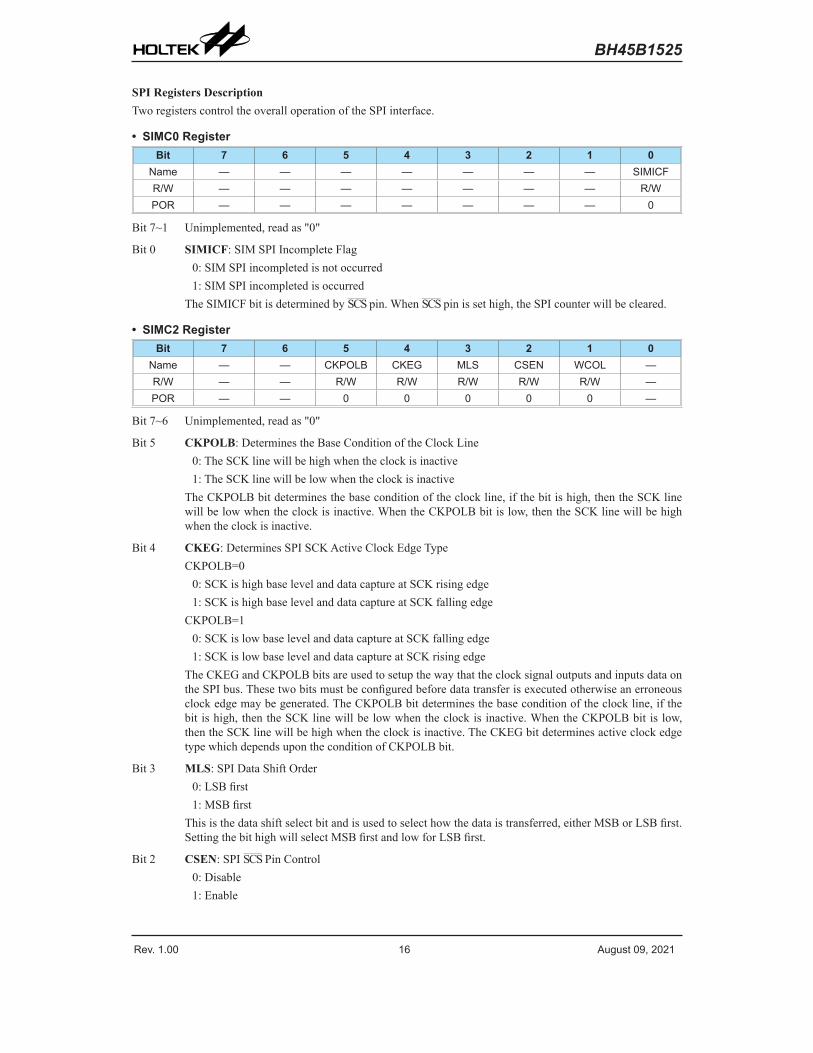
Bit 5 CKPOLB: Determines the Base Condition of the Clock Line0: The SCK line will be high when the clock is inactive1: The SCK line will be low when the clock is inactive
The CKPOLB bit determines the base condition of the clock line, if the bit is high, then the SCK line will be low when the clock is inactive. When the CKPOLB bit is low, then the SCK line will be high when the clock is inactive.
Bit 4 CKEG: Determines SPI SCK Active Clock Edge TypeCKPOLB=0
0: SCK is high base level and data capture at SCK rising edge1: SCK is high base level and data capture at SCK falling edge
CKPOLB=10: SCK is low base level and data capture at SCK falling edge1: SCK is low base level and data capture at SCK rising edge
The CKEG and CKPOLB bits are used to setup the way that the clock signal outputs and inputs data on the SPI bus. These two bits must be configured before data transfer is executed otherwise an erroneous clock edge may be generated. The CKPOLB bit determines the base condition of the clock line, if the bit is high, then the SCK line will be low when the clock is inactive. When the CKPOLB bit is low, then the SCK line will be high when the clock is inactive. The CKEG bit determines active clock edge type which depends upon the condition of CKPOLB bit.
Bit 3 MLS: SPI Data Shift Order0: LSB first1: MSB first
This is the data shift select bit and is used to select how the data is transferred, either MSB or LSB first. Setting the bit high will select MSB first and low for LSB first.
Bit 2 CSEN: SPI SCS Pin Control0: Disable1: Enable
Rev. 1.00 17 August 09, 2021
BH45B1525
The CSEN bit is used as an enable/disable for the SCS pin. If this bit is low, then the SCS pin will be disabled and placed into a floating condition. If the bit is high the SCS pin will be enabled and used as a select pin.
Bit 1 WCOL: SPI Write Collision Flag0: No collision1: Collision
The WCOL flag is used to detect if a data collision has occurred. If this bit is high it means that data has been attempted to be written to the SIMD register during a data transfer operation. This writing operation will be ignored if data is being transferred. The bit can be cleared by the application program.
Bit 0 Unimplemented, read as "0"
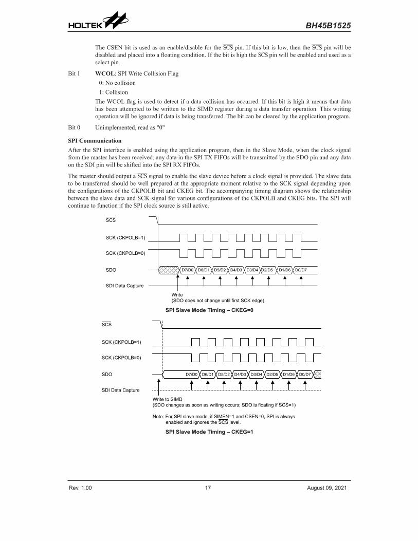
SPI CommunicationAfter the SPI interface is enabled using the application program, then in the Slave Mode, when the clock signal from the master has been received, any data in the SPI TX FIFOs will be transmitted by the SDO pin and any data on the SDI pin will be shifted into the SPI RX FIFOs.
The master should output a SCS signal to enable the slave device before a clock signal is provided. The slave data to be transferred should be well prepared at the appropriate moment relative to the SCK signal depending upon the configurations of the CKPOLB bit and CKEG bit. The accompanying timing diagram shows the relationship between the slave data and SCK signal for various configurations of the CKPOLB and CKEG bits. The SPI will continue to function if the SPI clock source is still active.
SCK (CKPOLB=1)
SCK (CKPOLB=0)
SCS
SDO
SDI Data Capture
Write(SDO does not change until first SCK edge)
D7/D0 D6/D1 D5/D2 D4/D3 D3/D4 D2/D5 D1/D6 D0/D7
SPI Slave Mode Timing – CKEG=0
SCK (CKPOLB=1)
SCK (CKPOLB=0)
SCS
SDO
SDI Data Capture
D7/D0 D6/D1 D5/D2 D4/D3 D3/D4 D2/D5 D1/D6 D0/D7
Write to SIMD(SDO changes as soon as writing occurs; SDO is floating if SCS=1)
Note: For SPI slave mode, if SIMEN=1 and CSEN=0, SPI is always enabled and ignores the SCS level.
SPI Slave Mode Timing – CKEG=1
Rev. 1.00 18 August 09, 2021
BH45B1525
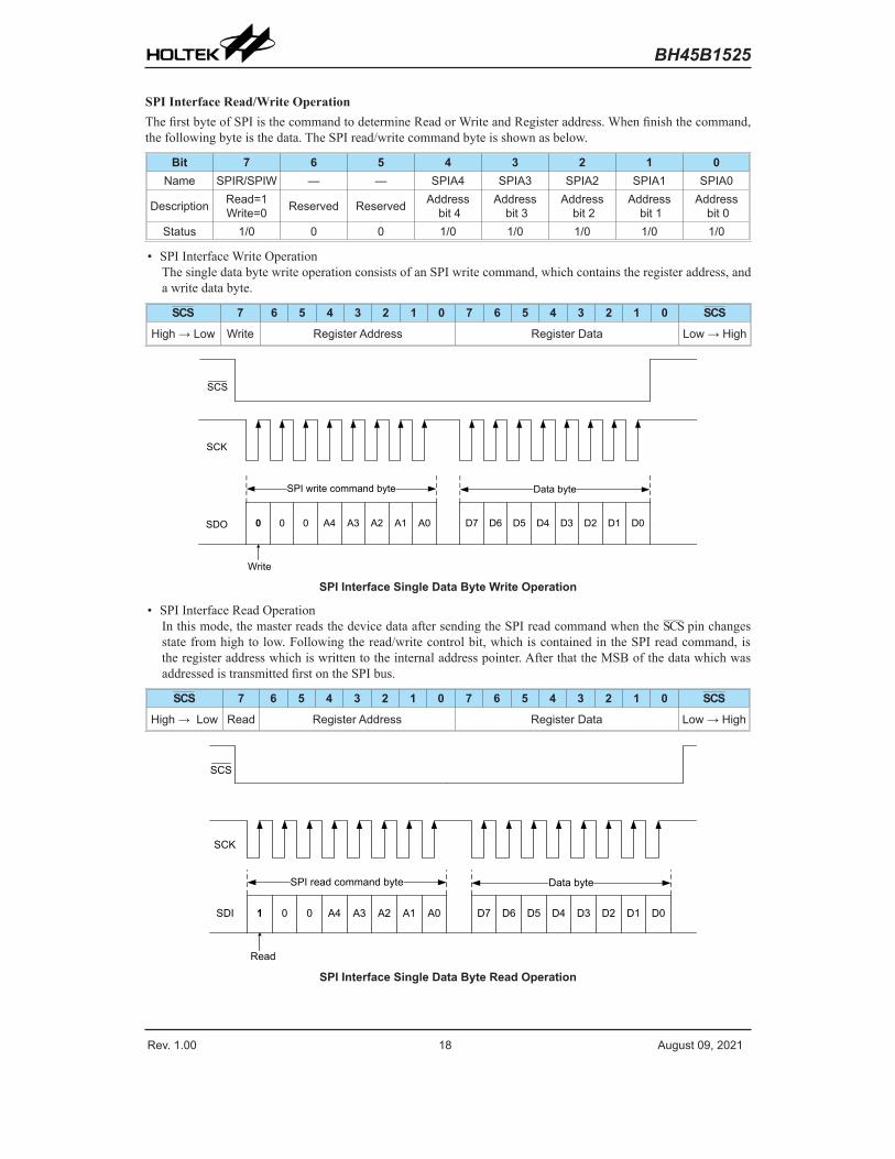
SPI Interface Read/Write OperationThe first byte of SPI is the command to determine Read or Write and Register address. When finish the command, the following byte is the data. The SPI read/write command byte is shown as below.
Bit 7 6 5 4 3 2 1 0Name SPIR/SPIW — — SPIA4 SPIA3 SPIA2 SPIA1 SPIA0
Description Read=1 Write=0 Reserved Reserved Address
bit 4Address
bit 3Address
bit 2Address
bit 1Address
bit 0Status 1/0 0 0 1/0 1/0 1/0 1/0 1/0
• SPI Interface Write OperationThe single data byte write operation consists of an SPI write command, which contains the register address, and a write data byte.
SCS 7 6 5 4 3 2 1 0 7 6 5 4 3 2 1 0 SCS
High → Low Write Register Address Register Data Low → High
D7 D6 D5 D4 D3 D2 D1 D0
SCS
SCK
SDO
SPI write command byte Data byte
0 0 0 A4 A3 A2 A1 A0
Write
SPI Interface Single Data Byte Write Operation
• SPI Interface Read OperationIn this mode, the master reads the device data after sending the SPI read command when the SCS pin changes state from high to low. Following the read/write control bit, which is contained in the SPI read command, is the register address which is written to the internal address pointer. After that the MSB of the data which was addressed is transmitted first on the SPI bus.
SCS 7 6 5 4 3 2 1 0 7 6 5 4 3 2 1 0 SCS
High → Low Read Register Address Register Data Low → High
1 A0 D7 D6 D5 D4 D3 D2 D1 D0
SCS
SCK
SDI
SPI read command byte Data byte
0 0 A4 A3 A2 A1
Read
SPI Interface Single Data Byte Read Operation
Rev. 1.00 19 August 09, 2021
BH45B1525
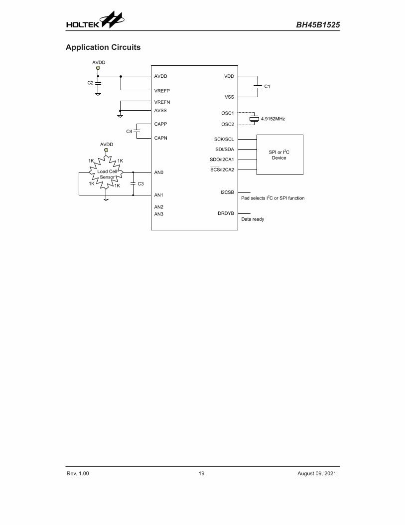
Application Circuits
C2
C4
AVDD
AN0
AN1
C3
1K
1K
1K
1K
Load Cell Sensor
CAPP
AVDD
AVSS
VREFP
VREFN
AVDD
VDD
VSS
C1
AN2AN3
SCK/SCL
SDO/I2CA1
OSC1
OSC2
I2CSB
CAPN
SDI/SDA
SCS/I2CA2
SPI or I2CDevice
Pad selects I2C or SPI function
4.9152MHz
DRDYBData ready
Rev. 1.00 20 August 09, 2021
BH45B1525
Package InformationNote that the package information provided here is for consultation purposes only. As this information may be updated at regular intervals users are reminded to consult the Holtek website for the latest version of the Package/Carton Information.
Additional supplementary information with regard to packaging is listed below. Click on the relevant section to be transferred to the relevant website page.
• Package Information (include Outline Dimensions, Product Tape and Reel Specifications)
• Packing Meterials Information
• Carton information
Rev. 1.00 21 August 09, 2021
BH45B1525
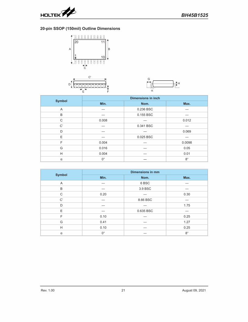
20-pin SSOP (150mil) Outline Dimensions
� �
�
� �
� �
� �
�
�
� �
� � ��
�
SymbolDimensions in inch
Min. Nom. Max.A — 0.236 BSC —B — 0.155 BSC —C 0.008 — 0.012 C’ — 0.341 BSC —D — — 0.069 E — 0.025 BSC —F 0.004 — 0.0098 G 0.016 — 0.05 H 0.004 — 0.01 α 0° ― 8°
SymbolDimensions in mm
Min. Nom. Max.A — 6 BSC —B — 3.9 BSC —C 0.20 — 0.30 C’ — 8.66 BSC —D — — 1.75 E — 0.635 BSC —F 0.10 — 0.25 G 0.41 — 1.27 H 0.10 — 0.25 α 0° ― 8°
Rev. 1.00 22 August 09, 2021
BH45B1525
Copyright© 2021 by HOLTEK SEMICONDUCTOR INC.
The information appearing in this Data Sheet is believed to be accurate at the time of publication. However, Holtek assumes no responsibility arising from the use of the specifications described. The applications mentioned herein are used solely for the purpose of illustration and Holtek makes no warranty or representation that such applications will be suitable without further modification, nor recommends the use of its products for application that may present a risk to human life due to malfunction or otherwise. Holtek's products are not authorized for use as critical components in life support devices or systems. Holtek reserves the right to alter its products without prior notification. For the most up-to-date information, please visit our web site at http://www.holtek.com/en/.
Related Documents


