Basic MOS Device Physics Lecture 17 MSE 515

Welcome message from author
This document is posted to help you gain knowledge. Please leave a comment to let me know what you think about it! Share it to your friends and learn new things together.
Transcript

Basic MOS Device Physics
Lecture 17 MSE 515
Topics
• MOS Structure • MOS IV Characteristics • CCD
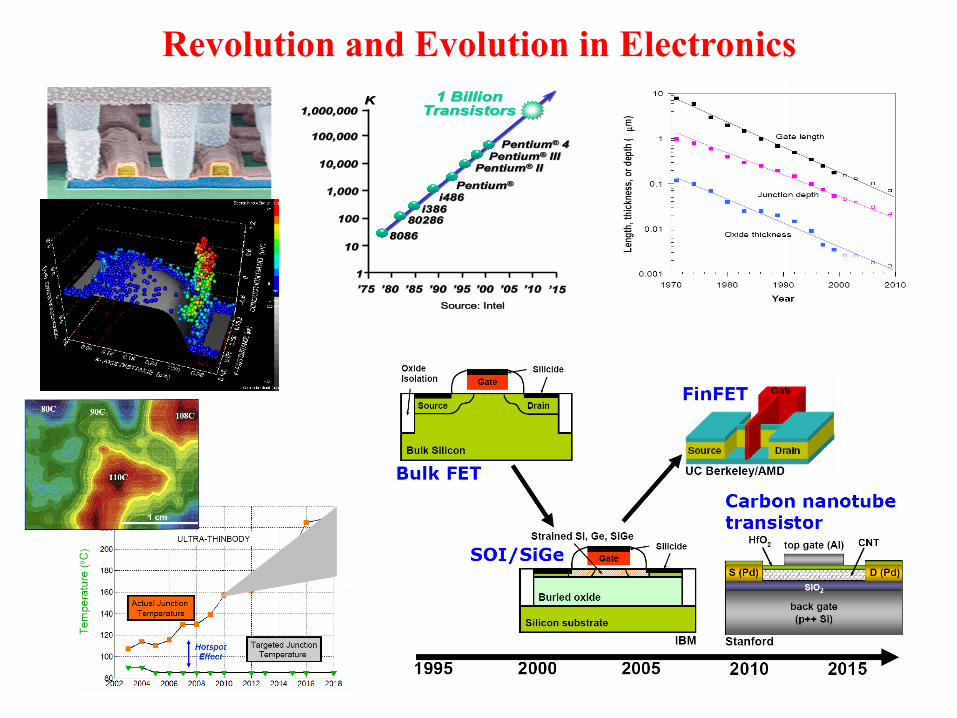
Revolution and Evolution in Electronics
Source: IntelSource: Intel
1,000,0001,000,000
100,000100,000
10,00010,000
1,0001,000
1010
100100
11
1 Billion 1 Billion TransistorsTransistors
808680868028680286
i386i386i486i486
PentiumPentium®®
KK
PentiumPentium®® IIII
’’7575 ’’8080 ’’8585 ’’9090 ’’9595 ’’0000 ’’0505 ’’1010
PentiumPentium®® IIIIIIPentiumPentium®® 44
’’1515Source: IntelSource: Intel
1,000,0001,000,000
100,000100,000
10,00010,000
1,0001,000
1010
100100
11
1 Billion 1 Billion TransistorsTransistors
808680868028680286
i386i386i486i486
PentiumPentium®®
KK
PentiumPentium®® IIII
’’7575 ’’8080 ’’8585 ’’9090 ’’9595 ’’0000 ’’0505 ’’1010
PentiumPentium®® IIIIIIPentiumPentium®® 44
’’1515
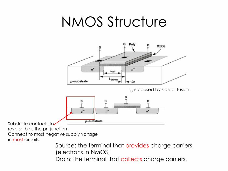
NMOS Structure
LD is caused by side diffusion
Source: the terminal that provides charge carriers. (electrons in NMOS) Drain: the terminal that collects charge carriers.
Substrate contact--to reverse bias the pn junction Connect to most negative supply voltage in most circuits.
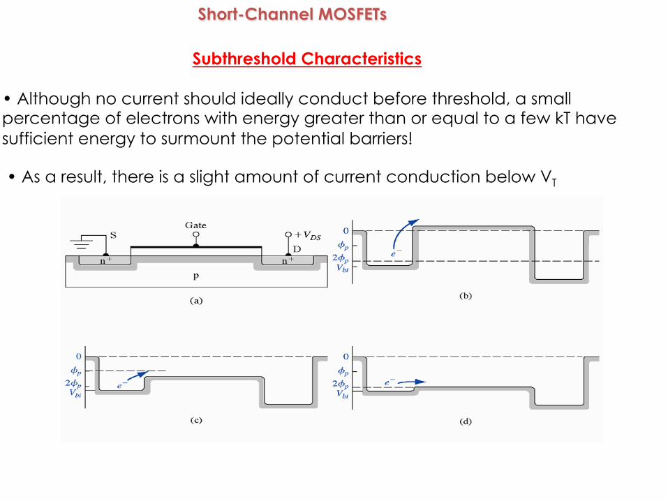
• Although no current should ideally conduct before threshold, a small percentage of electrons with energy greater than or equal to a few kT have sufficient energy to surmount the potential barriers!
Subthreshold Characteristics
Short-Channel MOSFETs
• As a result, there is a slight amount of current conduction below VT

Potential contours in a long channel MOSFET.
In a long channel MOSFET, the potential is uniform and parallel to the gate.
Short-Channel MOSFETs

Narrow Width Effect
• If the Polysilicon gate is atop the region of a LOCOS isolation where the oxide is increasing in thickness.
• It is possible to form a channel under LOCOS away from the thin gate oxide! This is quite important for devices with L < 1 mm.
Short-Channel MOSFETs

CMOS Structure
PMOS NMOS
Reverse bias the pn junction
Reverse bias the pn junction
Connect to most positive supply voltage in most circuits.

MOS IV Characteristics
• Threshold Voltage • Derivation of I/V Characteristics – I-V curve – Transconductance – Resistance in the linear region
• Second Order Effect – Body Effect – Channel Length Modulation – Subthreshold conduction

Threshold Voltage
1. Holes are expelled from the gate area 2. Depletion region (negative ions) is
created underneath the gate. 3. No current flows because no charge
carriers are available.
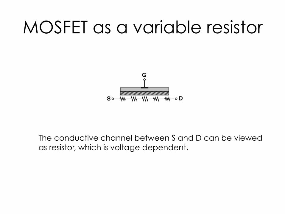
MOSFET as a variable resistor
The conductive channel between S and D can be viewed as resistor, which is voltage dependent.
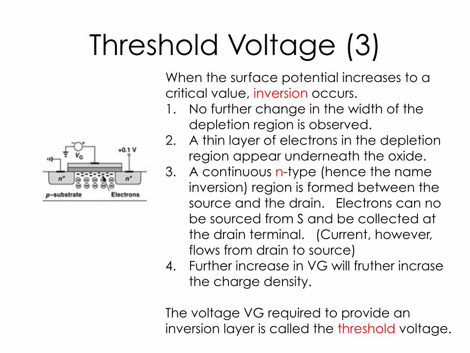
Threshold Voltage (3) When the surface potential increases to a critical value, inversion occurs. 1. No further change in the width of the
depletion region is observed. 2. A thin layer of electrons in the depletion
region appear underneath the oxide. 3. A continuous n-type (hence the name
inversion) region is formed between the source and the drain. Electrons can no be sourced from S and be collected at the drain terminal. (Current, however, flows from drain to source)
4. Further increase in VG will fruther incrase the charge density.
The voltage VG required to provide an inversion layer is called the threshold voltage.

Implantation of p+ dopants to alter the threshold
Threshold voltage can be adjusted by implanting Dopants into the channel area during fabrication. E.g. Implant p+ material to increase threshold voltage.
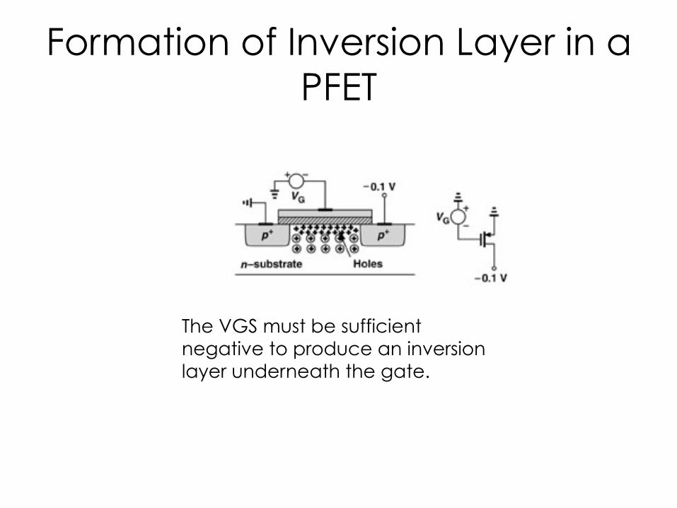
Formation of Inversion Layer in a PFET
The VGS must be sufficient negative to produce an inversion layer underneath the gate.
I-V Characteristics
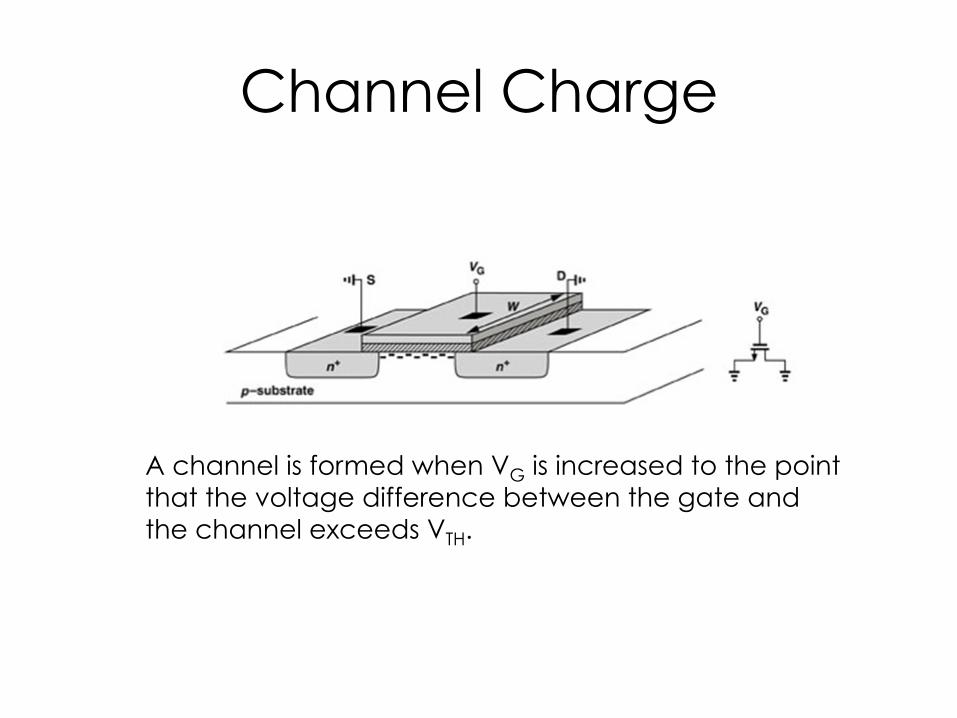
Channel Charge
A channel is formed when VG is increased to the point that the voltage difference between the gate and the channel exceeds VTH.

Application of VDS
What happens when you introduce a voltage at the drain terminal?

Channel Potential Variation
VX the voltage along the channel
VX increases as you move from S to D.
VG-VX is reduced as you move from S to D.
E.g. VS=0, VG=0.6, VD=0.6 At x=0, VG-VX=0.6 (more than VTH) At x=L, VG-VX=0 (less than VTH)
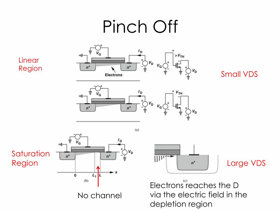
Pinch Off
Small VDS
Large VDS
No channel Electrons reaches the D via the electric field in the depletion region
Saturation Region
Linear Region
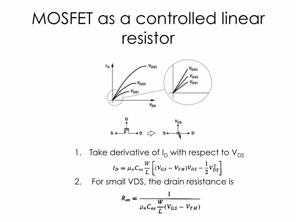
MOSFET as a controlled linear resistor
1. Take derivative of ID with respect to VDS
2. For small VDS, the drain resistance is

Transistor in Saturation Region
• I-V characteristics • Transconductance • Output resistance • Body transconductance
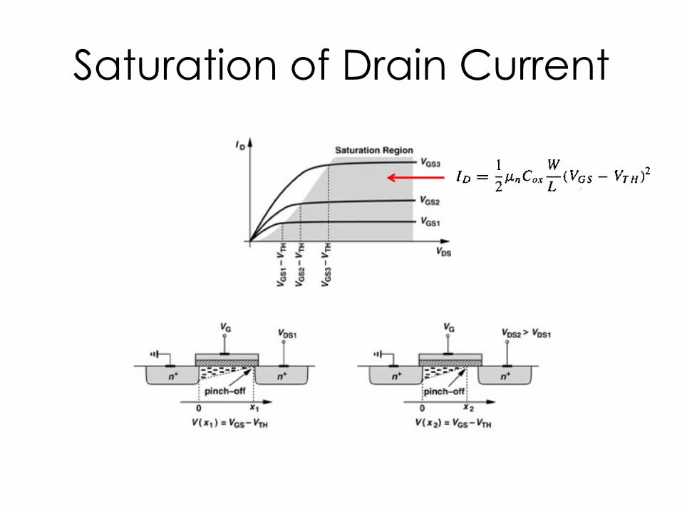
Saturation of Drain Current
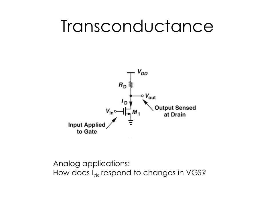
Transconductance
Analog applications: How does Ids respond to changes in VGS?
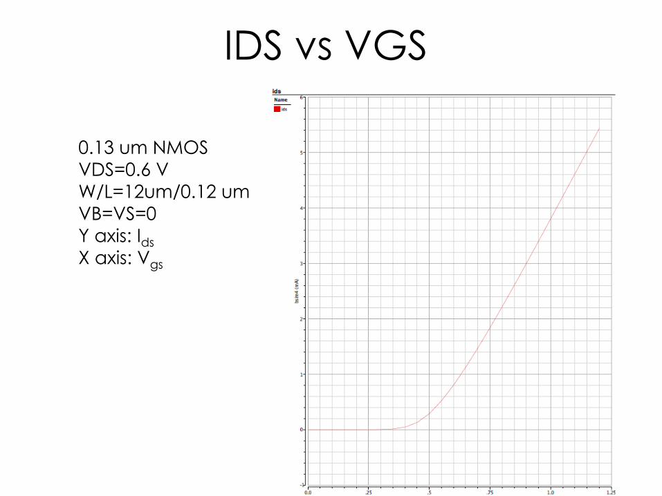
IDS vs VGS
0.13 um NMOS VDS=0.6 V W/L=12um/0.12 um VB=VS=0 Y axis: Ids X axis: Vgs
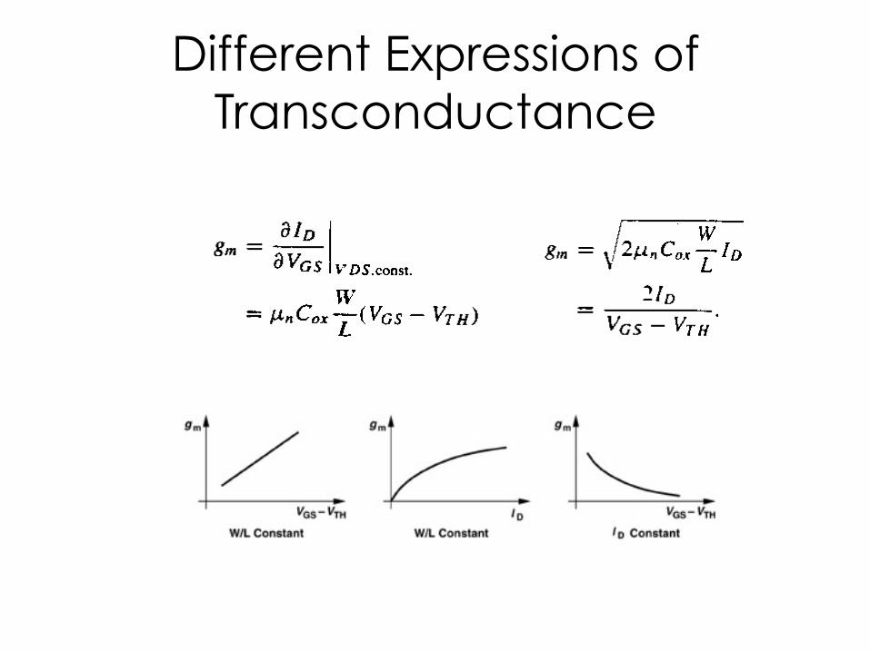
Different Expressions of Transconductance
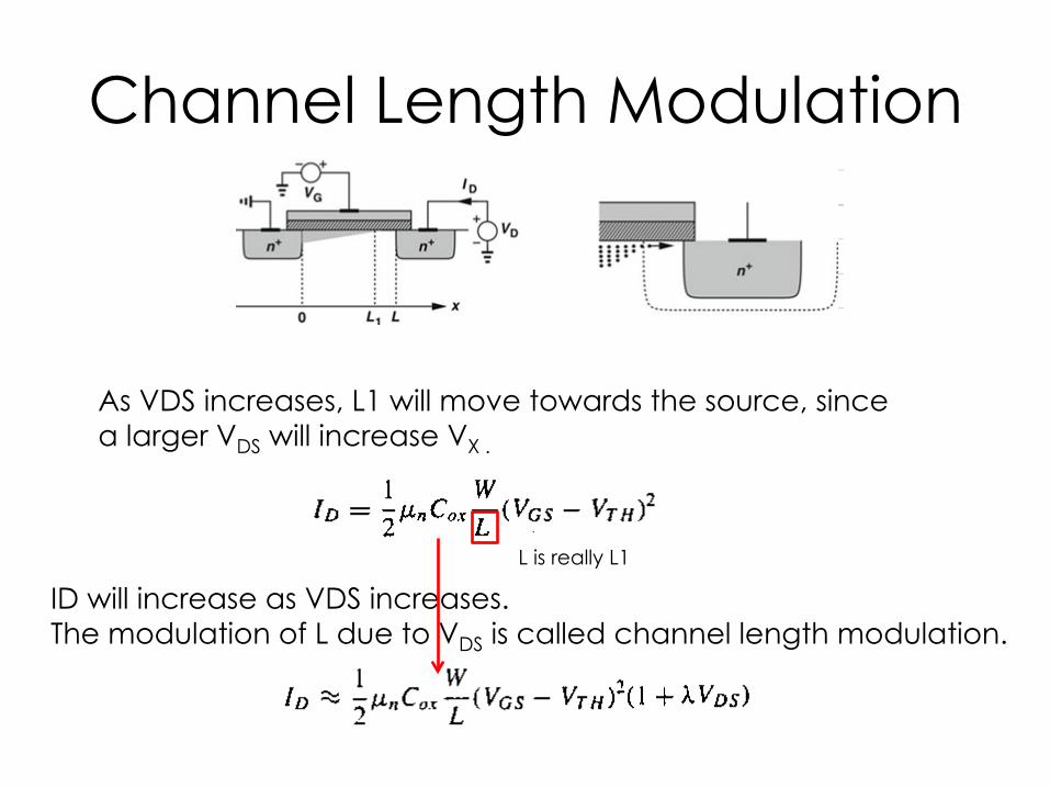
Channel Length Modulation
As VDS increases, L1 will move towards the source, since a larger VDS will increase VX .
L is really L1
ID will increase as VDS increases. The modulation of L due to VDS is called channel length modulation.

Controlling channel modulation
For a longer channel length, the relative change in L and Hence ID for a given change in VDS is smaller. Therefore, to minimize channel length modulation, minimum length transistors should be avoided.
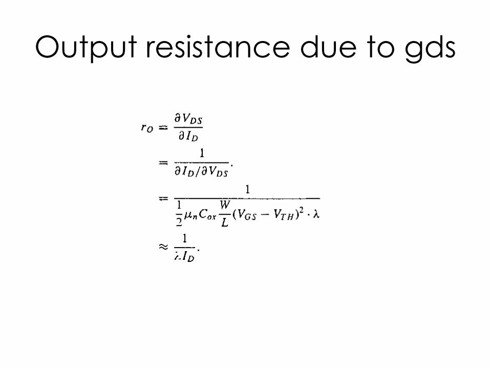
Output resistance due to gds
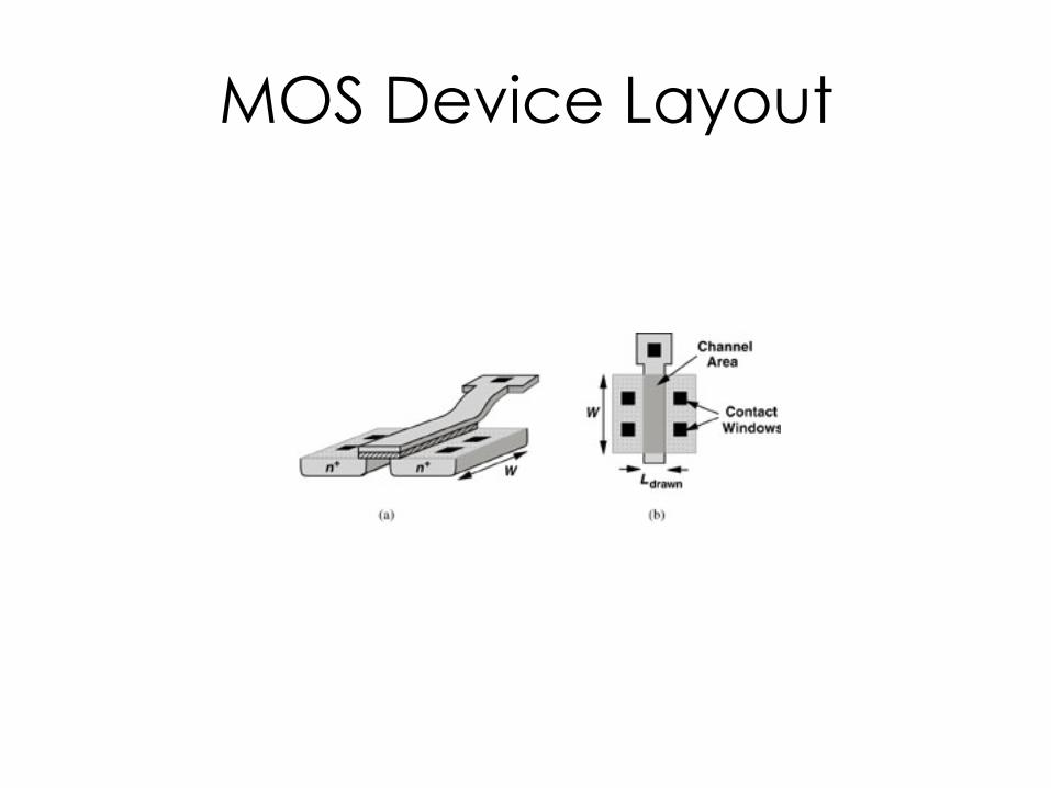
MOS Device Layout
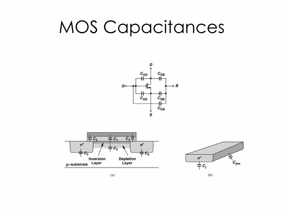
MOS Capacitances
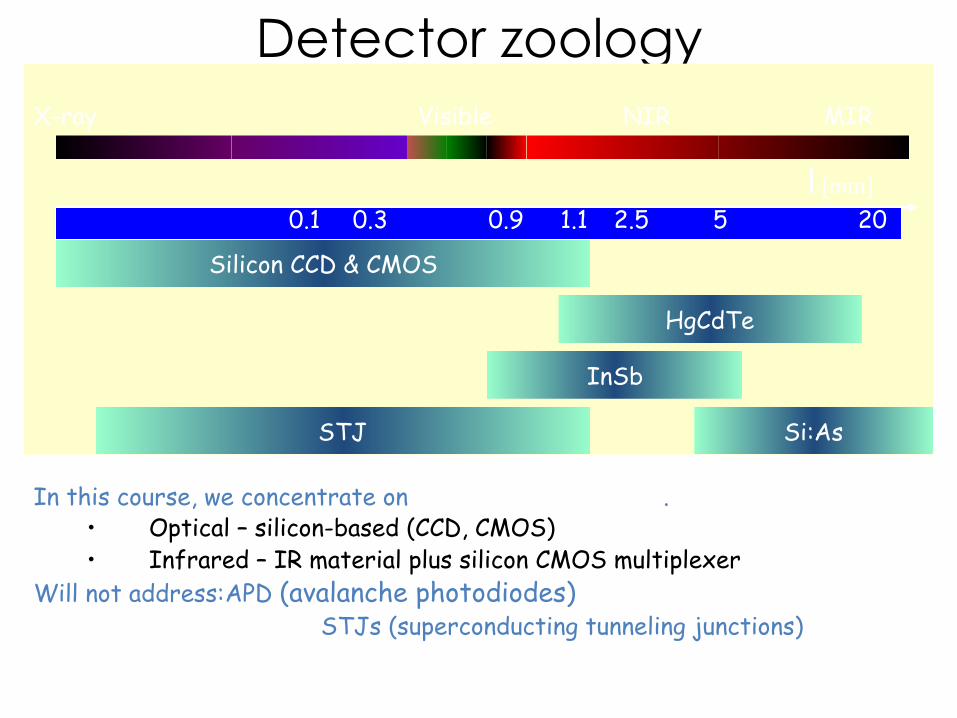
Detector zoology X-ray Visible NIR MIR
l [mm]
Silicon CCD & CMOS
0.3 1.1 0.9 2.5 5 20
HgCdTe
InSb
STJ
0.1
Si:As
In this course, we concentrate on 2-D focal plane arrays. • Optical – silicon-based (CCD, CMOS) • Infrared – IR material plus silicon CMOS multiplexer
Will not address: APD (avalanche photodiodes) STJs (superconducting tunneling junctions)
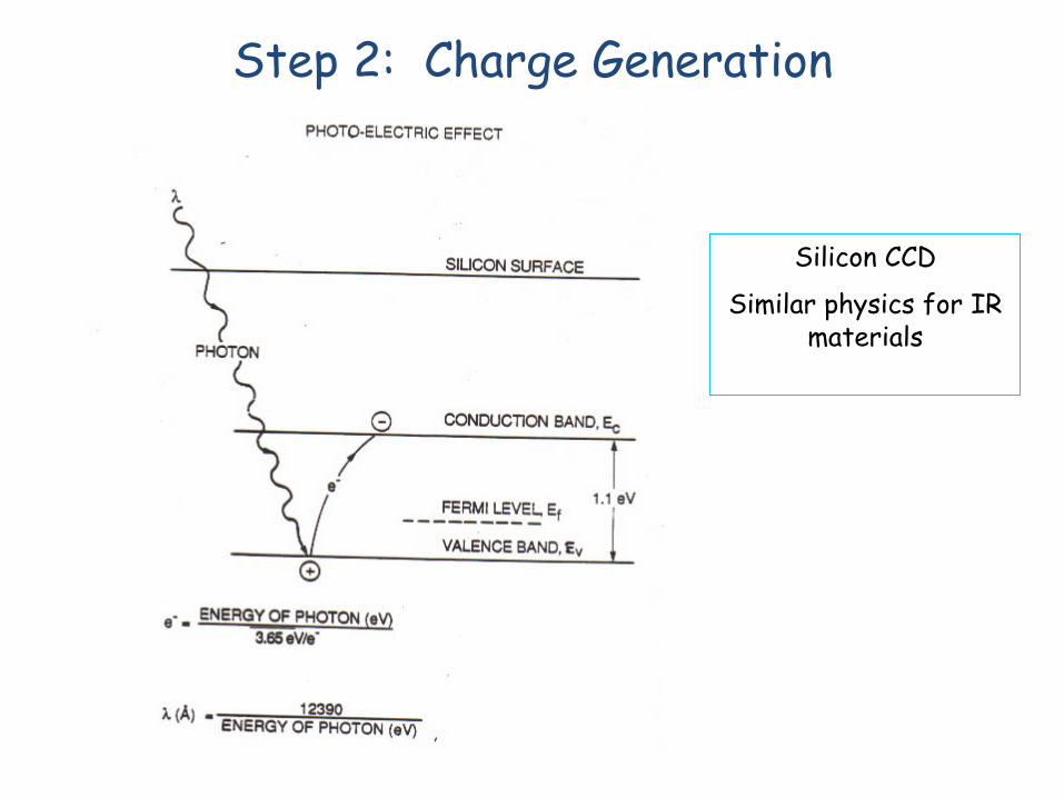
Step 2: Charge Generation
Silicon CCD
Similar physics for IR materials
33
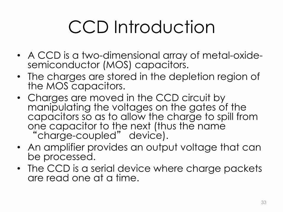
CCD Introduction • A CCD is a two-dimensional array of metal-oxide-
semiconductor (MOS) capacitors. • The charges are stored in the depletion region of
the MOS capacitors. • Charges are moved in the CCD circuit by
manipulating the voltages on the gates of the capacitors so as to allow the charge to spill from one capacitor to the next (thus the name “charge-coupled” device).
• An amplifier provides an output voltage that can be processed.
• The CCD is a serial device where charge packets are read one at a time.

34
Potential in MOS Capacitor

35
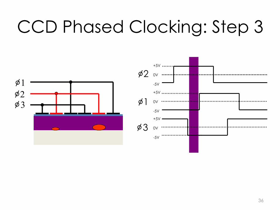
CCD Phased Clocking: Summary
36
1 2 3
CCD Phased Clocking: Step 3
+5V 0V -5V
+5V 0V -5V
+5V 0V -5V
1
2
3
37
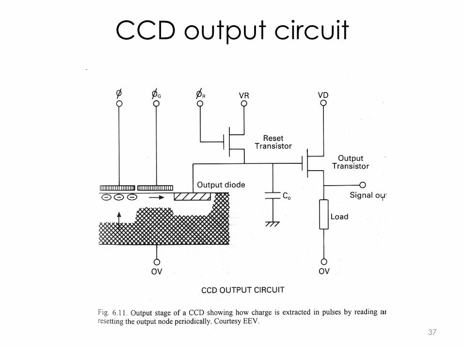
CCD output circuit

38
Charge Transfer Efficiency • When the wells are nearly empty, charge can be trapped by
impurities in the silicon. So faint images can have tails in the vertical direction.
• Modern CCDs can have a charge transfer efficiency (CTE) per transfer of 0.9999995, so after 2000 transfers only 0.1% of the charge is lost.
good CTE bad CTE

39

Threshold Voltage
• VG=0.6 V • VD=1.2 V • CMOS: 0.13 um • W/L=12um/0.12 um • NFET

I-V characteristic Equation for PMOS transistor
More on Body Effect
• Example • Analysis • gmbs
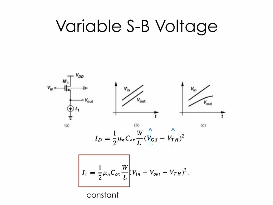
Variable S-B Voltage
constant
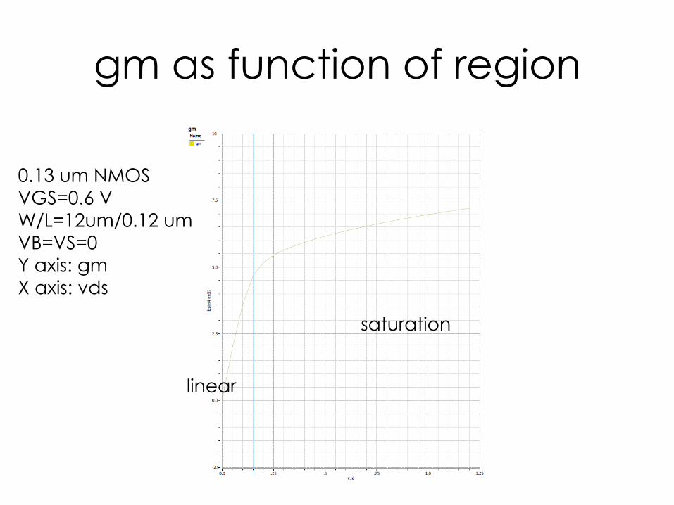
gm as function of region
saturation
0.13 um NMOS VGS=0.6 V W/L=12um/0.12 um VB=VS=0 Y axis: gm X axis: vds
linear
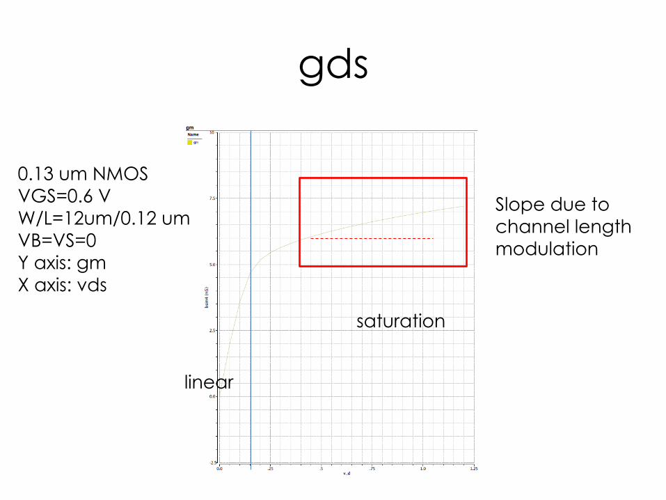
gds
saturation
0.13 um NMOS VGS=0.6 V W/L=12um/0.12 um VB=VS=0 Y axis: gm X axis: vds
linear
Slope due to channel length modulation
Body Effect
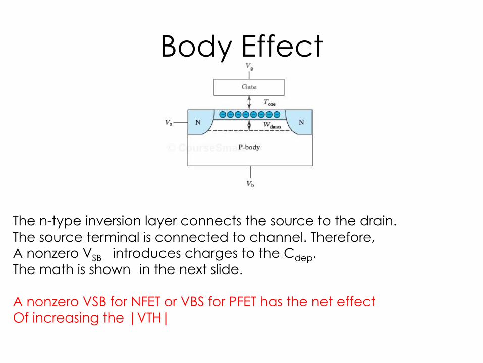
The n-type inversion layer connects the source to the drain. The source terminal is connected to channel. Therefore, A nonzero VSB introduces charges to the Cdep. The math is shown in the next slide. A nonzero VSB for NFET or VBS for PFET has the net effect Of increasing the |VTH|

Experimental Data of Body Effect
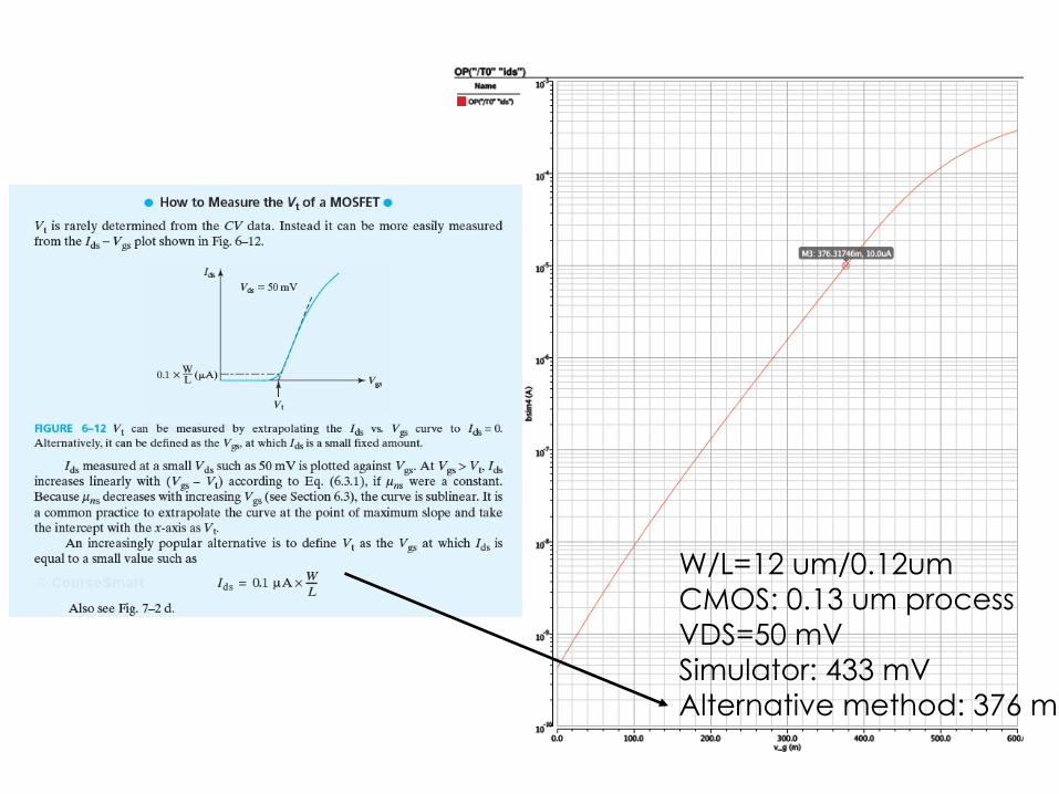
W/L=12 um/0.12um CMOS: 0.13 um process VDS=50 mV Simulator: 433 mV Alternative method: 376 mV

Subthreshold current
Subtreshold region
As VG increases, the surface potential will increase. There is very little majority carriers underneath the gate. There are two pn junctions. (B-S and B-D) The density of the minority carrier depends on the difference in the voltage across the two pn junction diode. A diffusion current will result the electron densities at D and S are not identical.
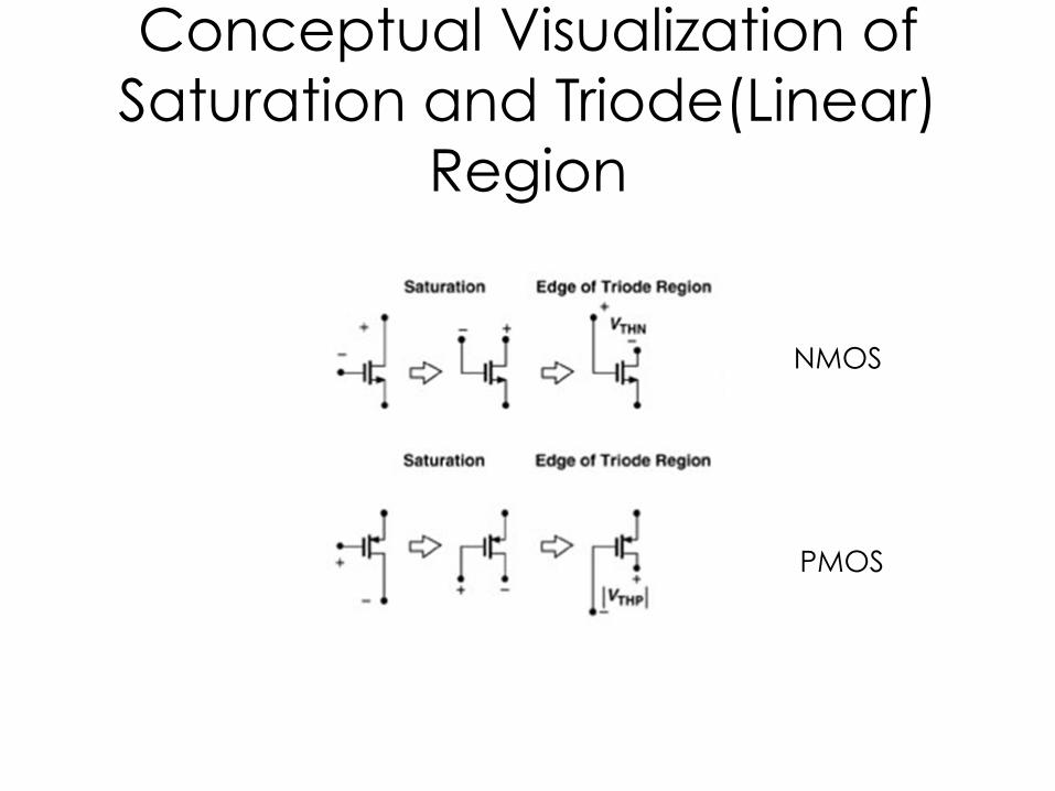
Conceptual Visualization of Saturation and Triode(Linear)
Region
NMOS
PMOS
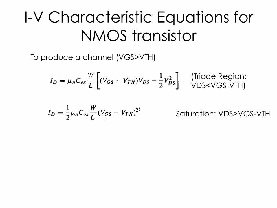
I-V Characteristic Equations for NMOS transistor
(Triode Region: VDS<VGS-VTH)
Saturation: VDS>VGS-VTH
To produce a channel (VGS>VTH)
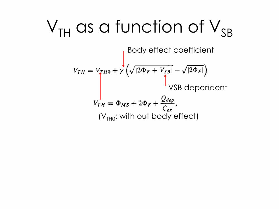
VTH as a function of VSB
(VTH0: with out body effect)
Body effect coefficient
VSB dependent
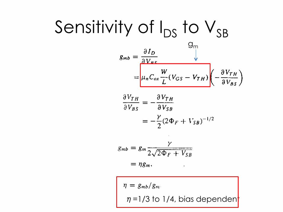
Sensitivity of IDS to VSB
(chain rule)
gm
η=1/3 to 1/4, bias dependent
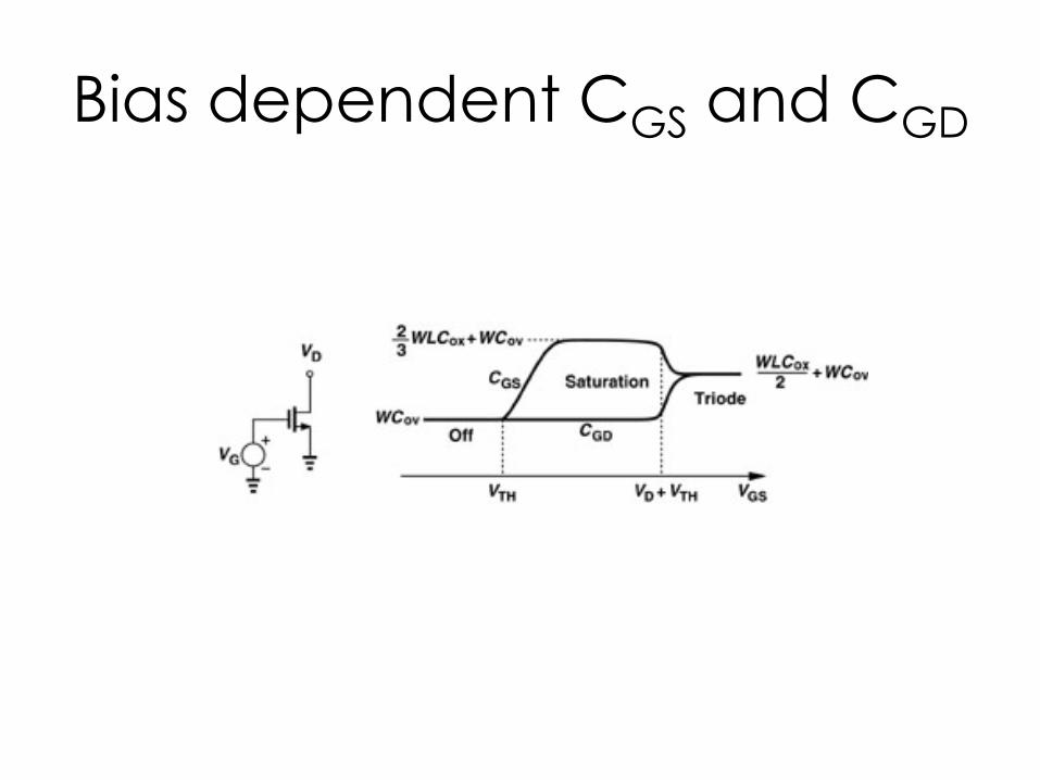
Bias dependent CGS and CGD
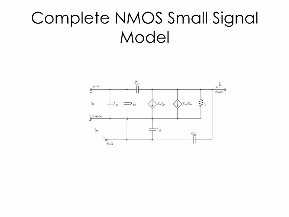
Complete NMOS Small Signal Model
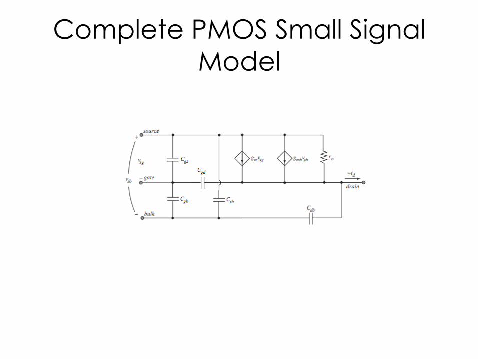
Complete PMOS Small Signal Model
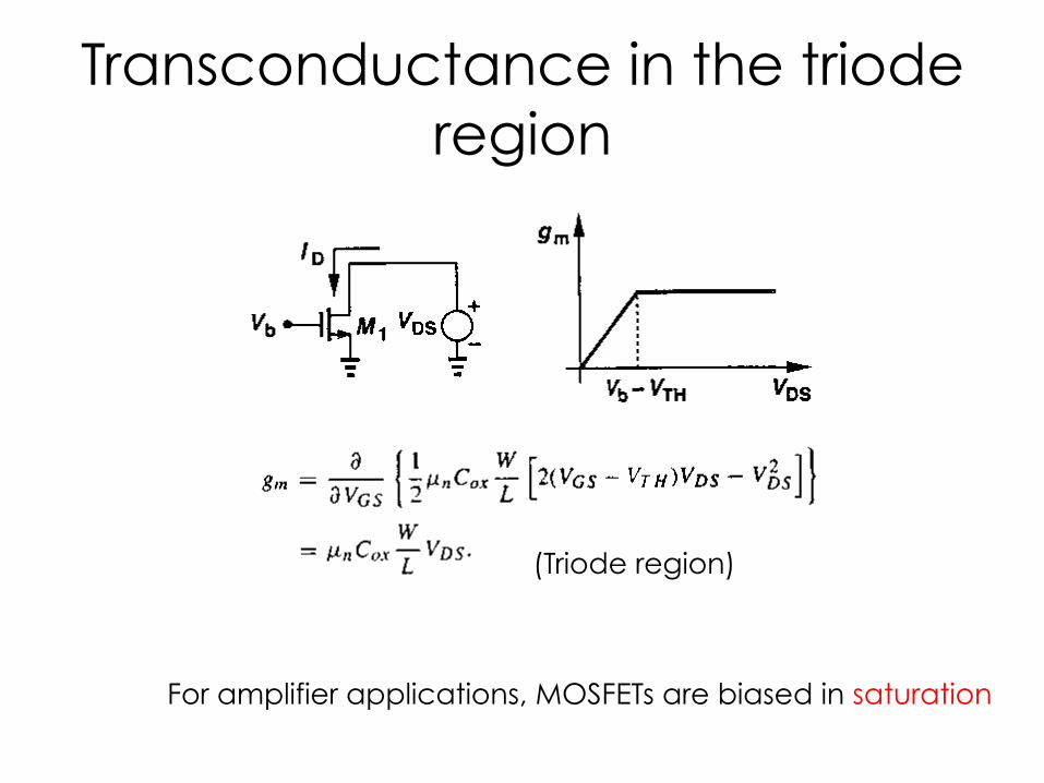
Transconductance in the triode region
(Triode region)
For amplifier applications, MOSFETs are biased in saturation
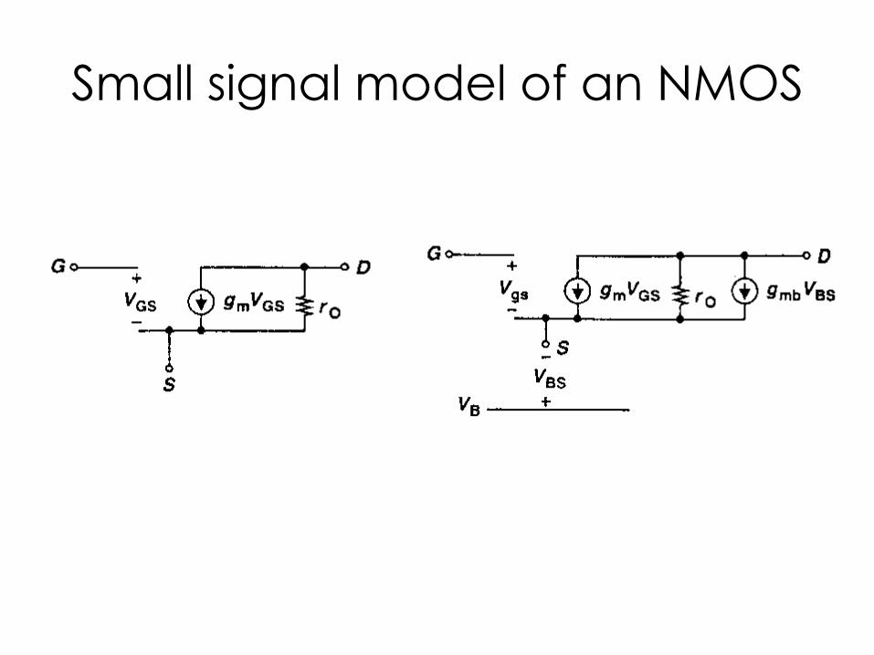
Small signal model of an NMOS

Small Signal Model
• If the bias current and voltages of a MOSFET are only disturbed slightly by signals, the nonlinear amd large signal model an be reduced to linear and small signal representation.
Related Documents


