Chapter 01 MicroChemicals ® – Fundamentals of Microstructuring www.MicroChemicals.com [email protected] Basics of Microstructuring www.microchemicals.com/downloads/application_notes.html DEVELOPMENT After exposure, the future resist mask exists as a latent image in the photo-resist: The exposed areas di ffer chemically from the non-exposed sites. The purpose of the development is to dissolve either the exposed (in the case of positive resists) or the unexposed (in the case of negative resists) resist areas, resulting in the final desired resist structures. This chapter discusses the basic chemical and physical processes during development and explains the impact of different process parameters on the development rate and selectivity of the development process. Basic Chemistry of Developers Aqueous Alkaline Developers The positive and negative resists we market are usually developed aqueous-alkaline. The corresponding developers are based either on a diluted sodium hydroxide or potassium hydroxide solution or on an aqueous solution of the metal ion free organic TMAH (TetraMethylAmmoniumHydroxide). Many developers use chemical buffers against neutralisation by CO 2 to extend the shelf life, surface wet- ting agents for puddle development, and additives for removing tenacious resist residues. Opened developer containers should be stored well closed and not left open for an unnecessary length of time in order to prevent the ingress of CO 2 from the ambient air. CO 2 reduces the activity of the devel- oper after exhaustion of a possible chemical bu ffer and reduces its rate of development by decreasing the pH value and thus its activity. Open containers filled with developers also absorb CO 2 from the ambient air, where the ratio of surface to volume is decisive: Beakers should be changed at least daily, while larger tanks can remain stable for days and weeks. When the developer is protected by a nitrogen curtain in the process pauses, which is placed on the developer surface like a carpet, thus suppressing the CO 2 input, the shelf life is signi ficantly increased. Organic Solvents Cross-linked negative resists can generally also be developed with organic solvents in which the cross- linked resist areas are insoluble. However, caution is advised in the usually aqueous alkaline developable AZ ® negative resists which we market, as follows: If the resist is exposed to organic solvents too long, there is a risk that the cross-linked resist areas swell and subsequently separate from the substrate, de- Fig. 96: The schematic process of devel- opment of DNQ-based photoresists at the molecular level: In the unexposed state, the photoinitiator is located on the hydrophobic side of the phenolic resin chains, the indene carboxylic acid formed during exposure expands to the hydrophilic side. There, it separates a proton from the resin, which is thereby negatively charged and now soluble in aqueous al- kaline developers. Carbon atoms are shown here in black, hydrogen atoms light grey, oxygen at- oms blue, nitrogen atoms red, and sul- phur atoms yellow. Hydrophilic side of the phenolic resin chain Hydropho- bic side of the phenolic resin chain Unexposed photoinitiator Exposed photoinitiator (indene carboxylic acid) Depro- tonation

Welcome message from author
This document is posted to help you gain knowledge. Please leave a comment to let me know what you think about it! Share it to your friends and learn new things together.
Transcript
Chapter01 MicroChemicals® – Fundamentals of Microstructuring
www.MicroChemicals.com [email protected]
Basics of Microstructuringwww.microchemicals.com/downloads/application_notes.html
DEVELOPMENTAfter exposure, the future resist mask exists as a latent image in the photo-resist: The exposed areas diff er chemically from the non-exposed sites. The purpose of the development is to dissolve either the exposed (in the case of positive resists) or the unexposed (in the case of negative resists) resist areas, resulting in the fi nal desired resist structures.This chapter discusses the basic chemical and physical processes during development and explains the impact of diff erent process parameters on the development rate and selectivity of the development process.
Basic Chemistry of Developers
Aqueous Alkaline DevelopersThe positive and negative resists we market are usually developed aqueous-alkaline. The corresponding developers are based either on a diluted sodium hydroxide or potassium hydroxide solution or on an aqueous solution of the metal ion free organic TMAH (TetraMethylAmmoniumHydroxide).Many developers use chemical buff ers against neutralisation by CO2 to extend the shelf life, surface wet-ting agents for puddle development, and additives for removing tenacious resist residues.Opened developer containers should be stored well closed and not left open for an unnecessary length of time in order to prevent the ingress of CO2 from the ambient air. CO2 reduces the activity of the devel-oper after exhaustion of a possible chemical buff er and reduces its rate of development by decreasing the pH value and thus its activity.Open containers fi lled with developers also absorb CO2 from the ambient air, where the ratio of surface to volume is decisive: Beakers should be changed at least daily, while larger tanks can remain stable for days and weeks. When the developer is protected by a nitrogen curtain in the process pauses, which is placed on the developer surface like a carpet, thus suppressing the CO2 input, the shelf life is signifi cantly increased.
Organic SolventsCross-linked negative resists can generally also be developed with organic solvents in which the cross-linked resist areas are insoluble. However, caution is advised in the usually aqueous alkaline developable AZ® negative resists which we market, as follows: If the resist is exposed to organic solvents too long, there is a risk that the cross-linked resist areas swell and subsequently separate from the substrate, de-
Fig. 96: The schematic process of devel-opment of DNQ-based photoresists at the molecular level: In the unexposed state, the photoinitiator is located on the hydrophobic side of the phenolic resin chains, the indene carboxylic acid formed during exposure expands to the hydrophilic side.There, it separates a proton from the resin, which is thereby negatively charged and now soluble in aqueous al-kaline developers.Carbon atoms are shown here in black, hydrogen atoms light grey, oxygen at-oms blue, nitrogen atoms red, and sul-phur atoms yellow.
Hydrophilic side of the phenolic resin chain
Hydropho-bic side of
the phenolic resin chain
Unexposed photoinitiator
Exposed photoinitiator (indene carboxylic acid)
Depro-tonation
Chapter01 MicroChemicals® – Fundamentals of Microstructuring
www.MicroChemicals.com [email protected]
Basics of Microstructuringwww.microchemicals.com/downloads/application_notes.html
pending on the degree of cross-linking of the resist fi lm and its adhesion.
Selection Criteria of Developers
Compatibility with PhotoresistsNot every photoresist can be developed without residue with every developer. For example, the NaOH-based AZ® 351 is less suitable for the AZ® 4500 series than the KOH or TMAH-based developers are, while AZ® 111 XFS requires the AZ® 303 as a developer.If in the processing of negative resists via scattering, diff raction or refl ections, an unintended partial ex-posure of nominally dark resist areas is to be feared, the TMAH-based AZ® 826 MIF can be benefi cial. This developer contains an additive for the removal of slightly cross-linked resist areas.
Metal Ion Containing or Metal Ion Free?Metal ion-containing developers such as the NaOH-based AZ® 351B or the KOH-based AZ® 400K are gen-erally much cheaper than metal ion-free TMAH-based developers, without a fundamental diff erence in their performance or capacity.An important selection criterion for the optimal developer is therefore the question of whether the devel-oper has to be metal ion-free (MIF), or alternatively metal ion-containing (MIC) developers can be used. Metal-ion-freeness is, for example, a condition when it is absolutely neces-sary to exclude, that residues of sodi-um or potassium ions of the developer on the substrate diff use during sub-sequent high-temperature processes into the semiconductor substrate and aff ect its electronic properties there as impurities.Concentrate or ready-to-use?Metal ion-containing developers such as AZ® 351B, AZ® 400K or AZ® Develop-er are usually supplied as concentrate and diluted with DI water before appli-cation.The 2.38% TMAH-based AZ® 326 MIF, 726 MIF or 826 MIF are pre-diluted (ready-to-use) and slightly further di-luted only when the application re-quires it.
Compatibility with SubstratesThe compatibility of the developer with the substrate material used must also be considered: Most developers attack alkaline sensitive metals such as aluminium and copper as well as various compound semiconductors due to their high pH value of approximately 13, which also entails the risk of the etched material being carried over to other sites on the substrate.Our "AZ® Developer" (metal ion-containing, based on sodium metasilicate and phosphate) is optimised for minimal aluminium erosion and also attacks many other alkaline-sensitive materials far less than oth-er aqueous alkaline developers.
Compatibility with Equipment or Development ProcessFor the dip development (in beaker or tank) basically all developers are suitable. However, if a strong
0
2
4
6
8
10
12
14
2 3 4 5 6Dilution (H2O : AZ® 400K Ratio
0
100
200
300
400
2 3 4H2O : AZ® 400K
AZ® 9260
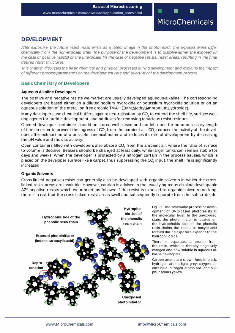
Fig. 97: The dark erosion rises with increasing developer concentration faster than the development rate so that the selectivity of the developer (plotted in the interior plot as a ratio of the development rate to the dark erosion) increases with the dilution. This experiment was carried out on a 30 μm thick AZ® 9260 layer baked at 100°C for 30 minutes at a developer temperature of 22°C.
Chapter01 MicroChemicals® – Fundamentals of Microstructuring
www.MicroChemicals.com [email protected]
Basics of Microstructuringwww.microchemicals.com/downloads/application_notes.html
mechanical recirculation of the developer is im-plemented, a foaming of, for example, surfactants added in the AZ® 726 MIF or 826 MIF may be problematic.Also in the course of spray development, the foam formation of surfactant-containing develop-ers can lead to an inhomogeneous developmen-tal pattern.However, these surfactants acting as wetting agents are a prerequisite for rapid and even wet-ting of the substrate in the puddle development resulting in a development result which is homo-geneous over the entire substrate.
Incompatibilities between MIC and MIF Develop-ersEven small traces of TMAH-based metal ion-free developers such as the AZ® 326 MIF, 726 MIF or 826 MIF) can signifi cantly reduce the develop-ment rate of metal ion-containing developers (such as the AZ® 400K or 351B).If both types of developers are used, extremely clean work is to be ensured to prevent mutual contamina-tion even in the ppm range, such as in the dispensing system or developer containers.
Development: Operations in the Photoresist on a Molecular Level
Positive Resists and Image Reversal ResistsThe exposure of our positive resists, our image reversal resists in the positive mode and the fl ood ex-posure of image reversal resists in the negative mode is based on the conversion of the DNQ-based photoinitiator in an indene carboxylic acid. The photoinitiator switches from the hydrophobic to the hy-drophilic side of the phenol resin chain where the OH bindings are located. Of this group the indene carboxylic acid splits a hydrogen ion, causing the resin molecule to be electrically charged ultimate-ly causing the increased solubility in developers.
Negative ResistsIn the case of negative resists, the unexposed res-in has a suffi ciently high physical solubility in de-velopers, whereas exposed and suffi ciently cross-linked resist areas show only negligible erosion.
Developer Concentration and Selectivity
Defi nition of SelectivityAs the selectivity of a developer, we refer here to the ratio of the dissolution rate of the resist to be developed to the dissolution rate of the resist structures, which should remain on the substrate.In the development of positive resists, the devel-opment rate (= the rate of erosion of the exposed resist) increases more intensely than dark erosion rate (= the eroded resist fi lm thickness of unex-posed photoresist per time) with the developer dilution, as shown in Fig. 97 based on a diff erently
1
1,2
1,4
1,6
1,8
2
2,2
2,4
2,6
2,8
3
12 15 18 21 24 27 30 33Developer Temperature (°C)
AZ 400K 1:4AZ 726MIF
AZ® 4562
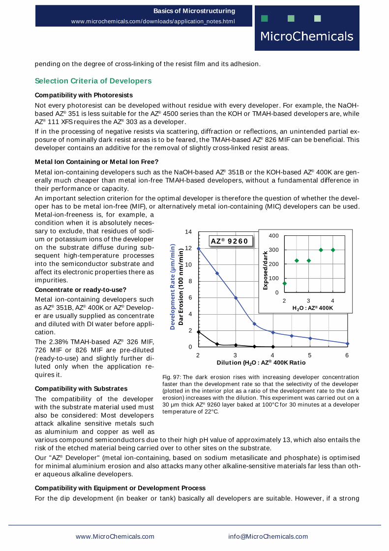
Fig. 98: The temperature dependence of the development rate measured as a mean value over the development of the entire resist fi lm on a 6 μm thick AZ® 4562 using the KOH-based AZ® 400K and TMAH-based AZ® 726 MIF.
®
®
®
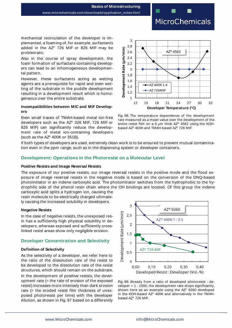
Fig. 99: Already from a ratio of developed photoresist : de-veloper = 1 : 1000, the development rate drops signifi cantly, shown here as an example using the AZ® 9260 developed in the KOH-based AZ® 400K and alternatively in the TMAH-based AZ® 726 MIF.
Chapter01 MicroChemicals® – Fundamentals of Microstructuring
www.MicroChemicals.com [email protected]
Basics of Microstructuringwww.microchemicals.com/downloads/application_notes.html
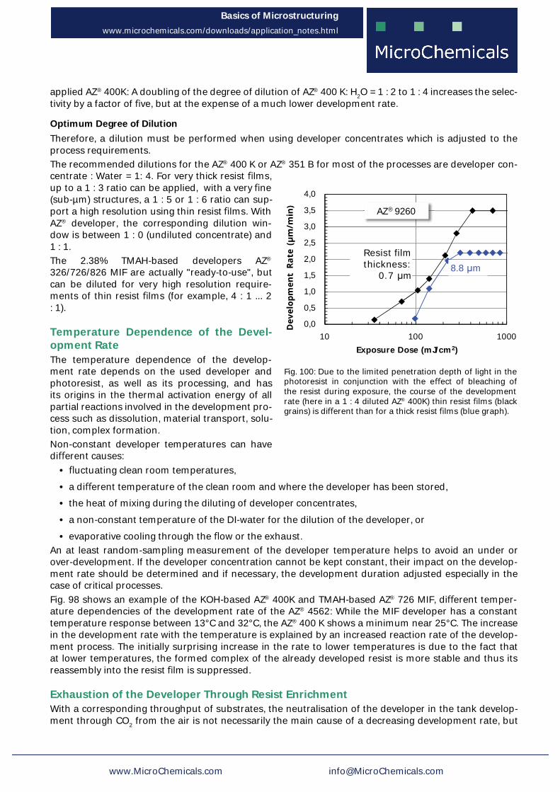
applied AZ® 400K: A doubling of the degree of dilution of AZ® 400 K: H2O = 1 : 2 to 1 : 4 increases the selec-tivity by a factor of fi ve, but at the expense of a much lower development rate.
Optimum Degree of DilutionTherefore, a dilution must be performed when using developer concentrates which is adjusted to the process requirements.The recommended dilutions for the AZ® 400 K or AZ® 351 B for most of the processes are developer con-centrate : Water = 1: 4. For very thick resist fi lms, up to a 1 : 3 ratio can be applied, with a very fi ne (sub-µm) structures, a 1 : 5 or 1 : 6 ratio can sup-port a high resolution using thin resist fi lms. With AZ® developer, the corresponding dilution win-dow is between 1 : 0 (undiluted concentrate) and 1 : 1.The 2.38% TMAH-based developers AZ® 326/726/826 MIF are actually "ready-to-use", but can be diluted for very high resolution require-ments of thin resist fi lms (for example, 4 : 1 ... 2 : 1).
Temperature Dependence of the Devel-opment RateThe temperature dependence of the develop-ment rate depends on the used developer and photoresist, as well as its processing, and has its origins in the thermal activation energy of all partial reactions involved in the development pro-cess such as dissolution, material transport, solu-tion, complex formation.Non-constant developer temperatures can have diff erent causes:
• fl uctuating clean room temperatures,
• a diff erent temperature of the clean room and where the developer has been stored,
• the heat of mixing during the diluting of developer concentrates,
• a non-constant temperature of the DI-water for the dilution of the developer, or
• evaporative cooling through the fl ow or the exhaust.An at least random-sampling measurement of the developer temperature helps to avoid an under or over-development. If the developer concentration cannot be kept constant, their impact on the develop-ment rate should be determined and if necessary, the development duration adjusted especially in the case of critical processes.Fig. 98 shows an example of the KOH-based AZ® 400K and TMAH-based AZ® 726 MIF, diff erent temper-ature dependencies of the development rate of the AZ® 4562: While the MIF developer has a constant temperature response between 13°C and 32°C, the AZ® 400 K shows a minimum near 25°C. The increase in the development rate with the temperature is explained by an increased reaction rate of the develop-ment process. The initially surprising increase in the rate to lower temperatures is due to the fact that at lower temperatures, the formed complex of the already developed resist is more stable and thus its reassembly into the resist fi lm is suppressed.
Exhaustion of the Developer Through Resist EnrichmentWith a corresponding throughput of substrates, the neutralisation of the developer in the tank develop-ment through CO2 from the air is not necessarily the main cause of a decreasing development rate, but
Fig. 100: Due to the limited penetration depth of light in the photoresist in conjunction with the eff ect of bleaching of the resist during exposure, the course of the development rate (here in a 1 : 4 diluted AZ® 400K) thin resist fi lms (black grains) is diff erent than for a thick resist fi lms (blue graph).
0,0
0,5
1,0
1,5
2,0
2,5
3,0
3,5
4,0
10 100 1000Exposure Dose (mJ/cm2)
Resist film thickness:
0.7 μm8.8 μm
AZ® 9260
Chapter01 MicroChemicals® – Fundamentals of Microstructuring
www.MicroChemicals.com [email protected]
Basics of Microstructuringwww.microchemicals.com/downloads/application_notes.html
the exhaustion through the already developed photoresist. Since diff erent photoinitiators absorb quite diff erently in the visible, the dyeing of the developer bath is not a suffi ciently accurate criterion for a nec-essary change of the developer batch.In the puddle or spray development, there is often the question of the optimum developer volume per substrate.A rule of thumb: If one per mill (volume or weight) of developed photoresist is already dissolved in the developer solution, the development rate drops noticeably, so a change of the developer at this time is therefore sensible. From a ratio of 1 : 100, a large fraction of the OH- ions are consumed in the developer, and the development rate drops towards zero.With increasing resist concentration in the developer, a rapid and suffi cient rinsing after development becomes more and more important in order to avoid resist residues on the freely developed surfaces of the substrate. For the optimisation (minimisation) of the developer consumption by tank development, a two-stage development can be useful, after the exhaustion of the fi rst developer bath, this is disposed of, replaced by the developer of the second tank and the latter is fi lled with fresh developer. In the puddle development of thick photoresist fi lms, two or more successive puddle steps are recommended, between which the exhausted developer is briefl y spun off without (!!) drying between the puddle steps.
Exposure Dose and Development Rate
Positive ResistsWith exposure of DNQ-based positive resists, the following mechanisms impact the course of the later development rate:
• The concentration of already converted photoinitiators decreases exponentially towards zero
• As a result of the bleaching of the resist, the exposure is carried out from the resist surface to the substrate especially with optically thick resist fi lms
• The development rate depends not on a linear function, but comparable to a step function of the photoinitiator converted by the concentration
Fig. 100 shows the eff ect of increasing light doses on the average development rate of an optically thin (penetration depth of the light > resist fi lm thickness) and optically thick (penetration depth < resist fi lm thickness): From a specifi c light dose, the photoinitiator is completely converted, the development rate is saturated. In the case of thick resist fi lms, exposure accompanied by bleaching proceeds from the resist surface towards the substrate so that the resist fi lm can be developed.
Negative Resists and Image Reversal ResistsThe development rate of negative resists and image reversal resists in the negative mode depends only indirectly on the structure-defi ning exposure dose, since the unexposed (negative resists) or, respectively, fl ood exposed (image reversal resists) areas are developed. However, these resist areas also receive a certain dose via diff raction and diff use light, as a result of which especially very fi ne structures are more diffi cult to develop with increasing exposure dose. In the case of image reversal resists, care must gen-erally be taken that the dose of the fl ood exposure is suffi cient to completely convert the photoinitiator.The erosion of the resist areas exposed through the photomask increases markedly below a certain light dose when the cross-linking or reversing reaction no longer takes place completely.
Surface Inhibition Layer
ImpactDeveloped positive resist structures sometimes show an overhang (“T-Topping”), which results from a suppressed development rate on the resist surface.Possible explanatory approaches for such a surface inhibition layer (not to be confused with the undercut desired in the case of negative or image reversal resists but attained by means of the reverse reaction) are controversially discussed in the literature. This eff ect is to be summarised here in the following with-out any claim to completeness, together with possible explanatory approaches:
Chapter01 MicroChemicals® – Fundamentals of Microstructuring
www.MicroChemicals.com [email protected]
Basics of Microstructuringwww.microchemicals.com/downloads/application_notes.html
Surface Cross-linkingThe deep-UV radiation around 250 nm wavelength which, with very low intensity, is also emitted during exposure with Hg lamps, as well as oxygen from air, break chemical bonds in the phenolic resin chains. In the case of subsequent baking steps (e.g. post exposure bake), resist areas near the surface can be cross-linked thermally activated and are thereby diffi cult to dissolve in the developer.In the case of non-extremely high exposure doses (as required, for example, in the processing of very thick resist fi lms), the proportionate low UV dose does not, however, result in a signifi cant cracking of phenolic resin chains; and the high diff usion constant of O2 in photoresist cannot explained thermally induced oxidation exclusively near the resist surface.
Spatial Segregation of Resist ComponentsThe diff erent boundary conditions (polar/non-polar) of the photoresist/air and the photoresist/substrate interfaces support spatial segregation of resin molecules - selected according to their molecular size - and theoretically permit the accumulation of resin components which are diffi cult to dissolve in the developer on the surface of the resist.Also the formation of spatial gradients of other resist components which impact on the development rate (especially the indene carboxylic acid or residual solvent formed during the exposure) are discussed in conjunction with the surface inhibition layer.
Delayed Start of DevelopmentThe - sometimes milky appearance observable with the bare eye - roughening of the resist surface to be developed during the development start increases the eff ective surface of the developer and explains the initially low development rate, but not the overhangs in the resist profi le mentioned at the beginning of this section.
Our Photoresists: Application Areas and Compatibilities
Recommended Applications 1 Resist Family Photoresists Resist Film Thickness 2 Recommended Developers 3 Recommended Re-
movers 4
1 In g
ener
al, a
lmos
t all
resi
sts
can
be u
sed
for a
lmos
t any
app
licat
ion.
How
ever
, the
spe
cial
pro
perti
es o
f eac
h re
sist
fam
ily
mak
es th
em s
peci
ally
sui
ted
for c
erta
in fi
elds
of a
pplic
atio
n.
2 Res
ist f
ilm th
ickn
ess
achi
evab
le a
nd p
roce
ssab
le w
ith s
tand
ard
equi
pmen
t und
er s
tand
ard
cond
ition
s. S
ome
resi
sts
can
be d
ilute
d fo
r low
er fi
lm th
ickn
esse
s; w
ith a
dditi
onal
effo
rt al
so th
icke
r res
ist f
ilms
can
be a
chie
ved
and
proc
esse
d.
3 Met
al io
n fre
e (M
IF) d
evel
oper
s ar
e si
gnifi
cant
ly m
ore
expe
nsiv
e, a
nd re
ason
able
if m
etal
ion
free
deve
lopm
ent i
s re
-qu
ired.
4 A
lso
depe
nds
on th
e re
sist
pro
cess
ing
and
subs
rrat
e m
ater
ials
use
d, d
etai
ls s
ee s
ectio
n ‘re
mov
ers’
nex
t pag
e
Posi
tive
Improved adhesion for wet etching, no focus on steep resist sidewalls
AZ® 1500
AZ® 1505 AZ® 1512 HS AZ® 1514 H AZ® 1518
≈ 0.5 µm ≈ 1.0 - 1.5 µm ≈ 1.2 - 2.0 µm ≈ 1.5 - 2.5 µm
AZ® 351B, AZ® 326 MIF, AZ® 726 MIF, AZ® Developer
AZ® 100 Remover, TechniStrip® P1316 TechniStrip® P1331
AZ® 4500 AZ® 4533 AZ® 4562
≈ 3 - 5 µm ≈ 5 - 10 µm AZ® 400K, AZ® 326 MIF, AZ® 726 MIF, AZ® 826 MIF
AZ® P4000
AZ® P4110 AZ® P4330 AZ® P4620 AZ® P4903
≈ 1 - 2 µm ≈ 3 - 5 µm
≈ 6 - 20 µm ≈ 10 - 30 µm
AZ® 400K, AZ® 326 MIF, AZ® 726 MIF, AZ® 826 MIF
AZ® PL 177 AZ® PL 177 ≈ 3 - 8 µm AZ® 351B, AZ® 400K, AZ® 326 MIF, AZ® 726 MIF, AZ® 826 MIF Spray coating AZ® 4999 ≈ 1 - 15 µm AZ® 400K, AZ® 326 MIF, AZ® 726 MIF, AZ® 826 MIF Dip coating MC Dip Coating Resist ≈ 2 - 15 µm AZ® 351B, AZ® 400K, AZ® 326 MIF, AZ® 726 MIF, AZ® 826 MIF
Steep resist sidewalls, high resolution and aspect ratio for e. g. dry etching or plating
AZ® ECI 3000 AZ® ECI 3007 AZ® ECI 3012 AZ® ECI 3027
≈ 0.7 µm ≈ 1.0 - 1.5 µm
≈ 2 - 4 µm AZ® 351B, AZ® 326 MIF, AZ® 726 MIF, AZ® Developer
AZ® 9200 AZ® 9245 AZ® 9260
≈ 3 - 6 µm ≈ 5 - 20 µm AZ® 400K, AZ® 326 MIF, AZ® 726 MIF
Elevated thermal softening point and high resolution for e. g. dry etching AZ® 701 MiR AZ® 701 MiR (14 cPs)
AZ® 701 MiR (29 cPs) ≈ 0.8 µm
≈ 2 - 3 µm AZ® 351B, AZ® 326 MIF, AZ® 726 MIF, AZ® Developer
Posi
tive
(che
m.
ampl
ified
)
Steep resist sidewalls, high resolution and aspect ratio for e. g. dry etching or plating
AZ® XT AZ® 12 XT-20PL-05 AZ® 12 XT-20PL-10 AZ® 12 XT-20PL-20 AZ® 40 XT
≈ 3 - 5 µm ≈ 6 - 10 µm
≈ 10 - 30 µm ≈ 15 - 50 µm
AZ® 400K, AZ® 326 MIF, AZ® 726 MIF AZ® 100 Remover, TechniStrip® P1316 TechniStrip® P1331
AZ® IPS 6050 ≈ 20 - 100 µm
Imag
e Re
-ve
rsal
Elevated thermal softening point and undercut for lift-off applications
AZ® 5200 AZ® 5209 AZ® 5214
≈ 1 µm ≈ 1 - 2 µm
AZ® 351B, AZ® 326 MIF, AZ® 726 MIF TechniStrip® Micro D2 TechniStrip® P1316 TechniStrip® P1331 TI TI 35ESX
TI xLift-X ≈ 3 - 4 µm ≈ 4 - 8 µm
Nega
tive
(Cro
ss-li
nkin
g)
Negative resist sidewalls in combination with no thermal softening for lift-off application
AZ® nLOF 2000 AZ® nLOF 2020 AZ® nLOF 2035 AZ® nLOF 2070
≈ 1.5 - 3 µm ≈ 3 - 5 µm
≈ 6 - 15 µm AZ® 326 MIF, AZ® 726 MIF, AZ® 826 MIF TechniStrip® NI555 TechniStrip® NF52 TechniStrip® MLO 07
AZ® nLOF 5500 AZ® nLOF 5510 ≈ 0.7 - 1.5 µm
Improved adhesion, steep resist side-walls and high aspect ratios for e. g. dry etching or plating
AZ® nXT
AZ® 15 nXT (115 cPs) AZ® 15 nXT (450 cPs)
≈ 2 - 3 µm ≈ 5 - 20 µm AZ® 326 MIF, AZ® 726 MIF, AZ® 826 MIF
AZ® 125 nXT ≈ 20 - 100 µm AZ® 326 MIF, AZ® 726 MIF, AZ® 826 MIF TechniStrip® P1316 TechniStrip® P1331 TechniStrip® NF52 TechniStrip® MLO 07
Our Developers: Application Areas and Compatibilities Inorganic Developers (typical demand under standard conditions approx. 20 L developer per L photoresist) AZ® Developer is based on sodium phosphate and –metasilicate, is optimized for minimal aluminum attack and is typically used diluted 1 : 1 in DI water for high contrast or undiluted for high development rates. The dark erosion of this developer is slightly higher compared to other developers. AZ® 351B is based on buffered NaOH and typically used diluted 1 : 4 with water, for thick resists up to 1 : 3 if a lower contrast can be tolerated. AZ® 400K is based on buffered KOH and typically used diluted 1 : 4 with water, for thick resists up to 1 : 3 if a lower contrast can be tolerated. AZ® 303 specifically for the AZ® 111 XFS photoresist based on KOH / NaOH is typically diluted 1 : 3 - 1 : 7 with water, depending on whether a high development rate, or a high contrast is required
Metal Ion Free (TMAH-based) Developers (typical demand under standard conditions approx. 5 - 10 L developer concentrate per L photoresist) AZ® 326 MIF is 2.38 % TMAH- (TetraMethylAmmoniumHydroxide) in water.

AZ® 726 MIF is 2.38 % TMAH- (TetraMethylAmmoniumHydroxide) in water, with additional surfactants for rapid and uniform wetting of the substrate (e. g. for puddle development) AZ® 826 MIF is 2.38 % TMAH- (TetraMethylAmmoniumHydroxide) in water, with additional surfactants for rapid and uniform wetting of the substrate (e. g. for puddle development) and other additives for the removal of poorly solu-ble resist components (residues with specific resist families), however at the expense of a slightly higher dark erosion.
Our Removers: Application Areas and Compatibilities AZ® 100 Remover is an amine solvent mixture and standard remover for AZ® and TI photoresists. To improve its performance, AZ® 100 remover can be heated to 60 - 80°C. Because the AZ ® 100 Remover reacts highly alkaline with water, it is suitable for this with respect to sensitive substrate materials such as Cu, Al or ITO only if contamination with water can be ruled out.. TechniStrip® P1316 is a remover with very strong stripping power for Novolak-based resists (including all AZ® positive resists), epoxy-based coatings, polyimides and dry films. At typical application temperatures around 75°C, TechniStrip® P1316 may dissolve cross-linked resists without residue also, e.g. through dry etching or ion implantation. TechniStrip® P1316 can also be used in spraying processes. For alkaline sensitive materials, TechniStrip® P1331 would be an alternative to the P1316. Nicht kompatibel mit Au oder GaAs. TechniStrip® P1331 can be an alternative for TechniStrip® P1316 in case of alkaline sensitive materials. TechniStrip® P1331 is not compatible with Au or GaAs. TechniStrip® NI555 is a stripper with very strong dissolving power for Novolak-based negative resists such as the AZ® 15 nXT and AZ® nLOF 2000 series and very thick positive resists such as the AZ® 40 XT. TechniStrip® NI555 was developed not only to peel cross-linked resists, but also to dissolve them without residues. This prevents contamination of the basin and filter by resist particles and skins, as can occur with standard strippers. TechniStrip ® NI555 is not compatible with Au or GaAs. TechniClean™ CA25 is a semi-aqueous proprietary blend formulated to address post etch residue (PER) removal for all interconnect and technology nodes. Extremely efficient at quickly and selectively removing organo-metal oxides from Al, Cu, Ti, TiN, W and Ni. TechniStrip™ NF52 is a highly effective remover for negative resists (liquid resists as well as dry films). The intrinsic nature of the additives and solvent make the blend totally compatible with metals used throughout the BEOL interconnects to WLP bumping applications. TechniStrip™ Micro D2 is a versatile stripper dedicated to address resin lift-off and dissolution on negative and positive tone resist. The organic mixture blend has the particularity to offer high metal and material compatibility allowing to be used on all stacks and particularly on fragile III/V substrates for instance. TechniStrip™ MLO 07 is a highly efficient positive and negative tone photoresist remover used for IR, III/V, MEMS, Photonic, TSV mask, solder bumping and hard disk stripping applications. Developed to address high dissolution performance and high material compatibility on Cu, Al, Sn/Ag, Alumina and common organic substrates.
Our Wafers and their Specifications Silicon-, Quartz-, Fused Silica and Glass Wafers Silicon wafers are either produced via the Czochralski- (CZ-) or Float zone- (FZ-) method. The more expensive FZ wafers are primarily reasonable if very high-ohmic wafers (> 100 Ohm cm) are required. Quartz wafers are made of monocrystalline SiO2, main criterion is the crystal orientation (e. g. X-, Y-, Z-, AT- or ST-cut) Fused silica wafers consist of amorphous SiO2. The so-called JGS2 wafers have a high transmission in the range of ≈ 280 - 2000 nm wavelength, the more expensive JGS1 wafers at ≈ 220 - 1100 nm. Our glass wafers, if not otherwise specified, are made of borosilicate glass. Specifications Common parameters for all wafers are diameter, thickness and surface (1- or 2-side polished). Fused silica wafers are made either of JGS1 or JGS2 material, for quartz wafers the crystal orientation needs to be defined. For silicon wafers, beside the crystal orientation (<100> or <111>) the doping (n- or p-type) as well as the resistivity (Ohm cm) are selection criteria. Prime- ,Test-, and Dummy Wafers Silicon wafers usually come as „Prime-grade“ or „Test-grade“, latter mainly have a slightly broader particle specification. „Dummy-Wafers“ neither fulfill Prime- nor Test-grade for different possible reasons (e. g. very broad or missing specification of one or several parameters, reclaim wafers, no particle specification) but might be a cheap alternative for e. g. resist coating tests or equipment start-up. Our Silicon-, Quartz-, Fused Silica and Glass Wafers Our frequently updated wafer stock list can be found here: è www.microchemicals.com/products/wafers/waferlist.html
Further Products from our Portfolio Plating Plating solutions for e. g. gold, copper, nickel, tin or palladium: è www.microchemicals.com/products/electroplating.html Solvents (MOS, VLSI, ULSI) Acetone, isopropyl alcohol, MEK, DMSO, cyclopentanone, butylacetate, ... è www.microchemicals.com/products/solvents.html Acids and Bases (MOS, VLSI, ULSI) Hydrochloric acid, sulphuric acid, nitric acid, KOH, TMAH, … è www.microchemicals.com/products/etchants.html Etching Mixtures for e. g. chromium, gold, silicon, copper, titanium, ... è www.microchemicals.com/products/etching_mixtures.html
Further Information Technical Data Sheets: www.microchemicals.com/downloads/product_data_sheets/photoresists.html Material Safety Data Sheets (MSDS): www.microchemicals.com/downloads/safety_data_sheets/msds_links.html
Our Photolithography Book and -Posters
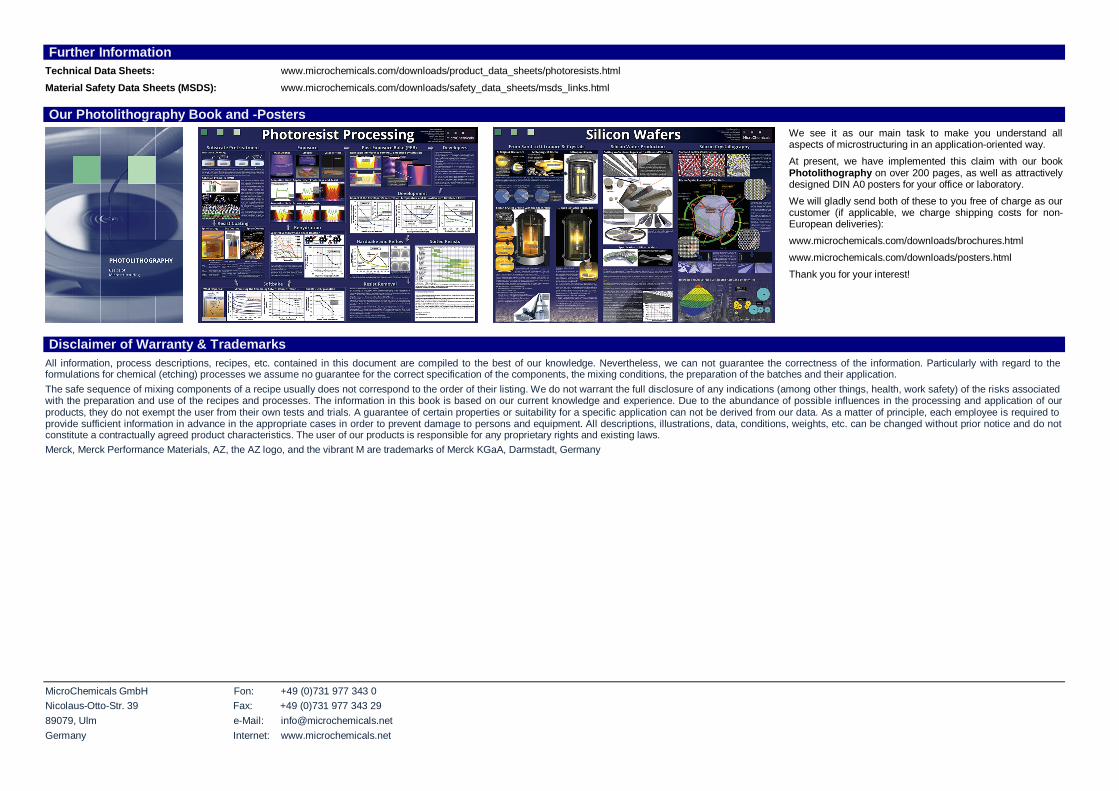
We see it as our main task to make you understand all aspects of microstructuring in an application-oriented way. At present, we have implemented this claim with our book Photolithography on over 200 pages, as well as attractively designed DIN A0 posters for your office or laboratory. We will gladly send both of these to you free of charge as our customer (if applicable, we charge shipping costs for non-European deliveries): www.microchemicals.com/downloads/brochures.html www.microchemicals.com/downloads/posters.html Thank you for your interest!
Disclaimer of Warranty & Trademarks All information, process descriptions, recipes, etc. contained in this document are compiled to the best of our knowledge. Nevertheless, we can not guarantee the correctness of the information. Particularly with regard to the formulations for chemical (etching) processes we assume no guarantee for the correct specification of the components, the mixing conditions, the preparation of the batches and their application. The safe sequence of mixing components of a recipe usually does not correspond to the order of their listing. We do not warrant the full disclosure of any indications (among other things, health, work safety) of the risks associated with the preparation and use of the recipes and processes. The information in this book is based on our current knowledge and experience. Due to the abundance of possible influences in the processing and application of our products, they do not exempt the user from their own tests and trials. A guarantee of certain properties or suitability for a specific application can not be derived from our data. As a matter of principle, each employee is required to provide sufficient information in advance in the appropriate cases in order to prevent damage to persons and equipment. All descriptions, illustrations, data, conditions, weights, etc. can be changed without prior notice and do not constitute a contractually agreed product characteristics. The user of our products is responsible for any proprietary rights and existing laws. Merck, Merck Performance Materials, AZ, the AZ logo, and the vibrant M are trademarks of Merck KGaA, Darmstadt, Germany MicroChemicals GmbH Fon: +49 (0)731 977 343 0 Nicolaus-Otto-Str. 39 Fax: +49 (0)731 977 343 29 89079, Ulm e-Mail: [email protected] Germany Internet: www.microchemicals.net
Related Documents