Banerjee, Archan (2017) Optimisation of superconducting thin film growth for next generation superconducting detector applications. PhD thesis. http://theses.gla.ac.uk/8573/ Copyright and moral rights for this work are retained by the author A copy can be downloaded for personal non-commercial research or study, without prior permission or charge This work cannot be reproduced or quoted extensively from without first obtaining permission in writing from the author The content must not be changed in any way or sold commercially in any format or medium without the formal permission of the author When referring to this work, full bibliographic details including the author, title, awarding institution and date of the thesis must be given Enlighten:Theses http://theses.gla.ac.uk/ [email protected]

Welcome message from author
This document is posted to help you gain knowledge. Please leave a comment to let me know what you think about it! Share it to your friends and learn new things together.
Transcript

Banerjee, Archan (2017) Optimisation of superconducting thin film growth for next generation superconducting detector applications. PhD thesis.
http://theses.gla.ac.uk/8573/
Copyright and moral rights for this work are retained by the author
A copy can be downloaded for personal non-commercial research or study, without prior
permission or charge
This work cannot be reproduced or quoted extensively from without first obtaining
permission in writing from the author
The content must not be changed in any way or sold commercially in any format or
medium without the formal permission of the author
When referring to this work, full bibliographic details including the author, title,
awarding institution and date of the thesis must be given
Enlighten:Theses
http://theses.gla.ac.uk/

Optimisation of superconducting thin film
growth for next generation
superconducting detector applications
Archan Banerjee
A thesis presented for the degree of
Doctor of Philosophy School of Engineering University of Glasgow
Scotland October, 2017

i
Abstract
There is a growing demand for superconducting detectors with single photon sensitivity from
near- to far infrared wavelengths. Emerging application areas include imaging, remote
sensing, astronomy and free space communications. Two superconducting device
technologies, superconducting nanowire single-photon detectors (SSPDs/SNSPDs) and
microwave kinetic inductance detectors (MKIDs) have the potential to outperform off-the-
self semiconductor technologies and offer scalability to large arrays. Fabrication of high
efficiency superconducting detectors strongly depends on the quality of superconducting
thin films. The original work presented in this thesis has explored the growth and
optimization of several superconducting thin film materials for next generation
superconducting detectors. Films have been grown in an ultra-high vacuum sputter
deposition system and an atomic layer deposition system.
Since its initial demonstration, NbN and NbTiN have been predominantly used as the base
material for SNSPDs. In this work, we have explored the optimization of both the materials
with an emphasis on NbTiN. NbTiN is optimized by heating the substrates to 800 C
achieving a Tc of 10.4 K for a film thickness of 5.5 nm on silicon substrate. Due to their
crystalline nature superconducting properties of NbN or NbTiN thin films are strongly
correlated with the lattice parameters of substrate properties. This causes a restriction on the
substrate choice and integration of SNSPD devices with complex circuits. Amorphous
superconducting materials can be promising alternatives for this purpose. We have explored
growth and optimization of amorphous MoSi and MoGe thin films. Both the materials are
co-sputtered to tune the composition. For 5 nm thick MoSi film on silicon substrate we
obtain Tc of 5.5 K. For MKID fabrication, TiN can be an useful base material due to its high
sheet resistance and widely tuneable superconducting properties. TiN thin films have been
sputtered on heated (500 C) silicon substrates with a Tc of 3.9 K for a 90 nm thick film. The
dielectric constants of the thin films as a function of wavelength (270-2200 nm) have been
determined via variable angle spectroscopic ellipsometry (VASE). Atomic structure and
stoichiometry of the films have been characterized in high resolution transmission electron
microscopy (HRTEM). This study enables us to precisely control film properties and thus
tailor superconducting films to the requirements of specific photon-counting applications.

ii
Contents
List of Acronyms and Symbols .......................................................................................................... vii
List of Figures ......................................................................................................................................... x
List of Tables ........................................................................................................................................ xiv
Chapter 1
Introduction…………………………………………………………………………………………………………..…………………..……. 1
Chapter 2
Background Review………………………………………………………………………………………………………….………… 6
2.1 Superconductivity ..................................................................................................................... 6
2.1.1 Theoretical Background of Superconductivity .................................................................. 8
2.2 Superconducting Materials ..................................................................................................... 13
2.3 Superconducting Thin Films ................................................................................................... 14
2.3.1 Theoretical Models describing correlation of superconductivity and material parameters
of Thin Films ............................................................................................................................. 15
2.3.2 Influence of growth conditions on film microstructures .................................................. 18
2.4 Detection of electromagnetic energy in superconductors ....................................................... 20
2.4.1 Superconducting Tunnel Junction .................................................................................... 20
2.4.2 Superconducting Transition-Edge Sensors ...................................................................... 21
2.5 Infrared single photon detection: Superconducting Nanowire Single Photon Detector
(SNSPD) ....................................................................................................................................... 23
2.5.1 Performance Parameters for SNSPDs .............................................................................. 25
2.5.2 Evolution of Device Design ............................................................................................. 28
2.5.3 Superconducting thin films for SNSPD ........................................................................... 29
2.5.4 Applications .................................................................................................................... 32
2.6 Terahertz radiation detection: Microwave Kinetic Inductance Detector (MKID) .................. 34
2.6.1 Performance Parameters for MKIDs ................................................................................ 35
2.6.2 Base material for MKID .................................................................................................. 36
2.6.3 Application of MKIDs ..................................................................................................... 37
2.7 Summary ............................................................................................................................. 38
References ..................................................................................................................................... 39
Chapter 3
Experimental Methods…………………………………………………………………………………………………….……..…46
3.1 Thin Film Growth ................................................................................................................... 46
3.1.1 Sputter Deposition System ............................................................................................... 46
3.1.2 Atomic Layer Deposition System .................................................................................... 52
3.2 Cryogen free Thin Film Testing Station ................................................................................. 54
3.2.1 Measurement of Critical Current Density ........................................................................ 61
iii
3.3 Thickness Measurement .......................................................................................................... 62
3.4 Transmission Electron Microscopy ........................................................................................ 63
3.4.1 Sample Preparation for HRTEM Analysis ....................................................................... 64
3.4.2 Working principle of Transmission Electron Microscopy ............................................... 65
3.5 Variable Angle Spectroscopic Ellipsometry (VASE) ............................................................. 69
3.6 Nanowire patterning of superconducting thin films................................................................ 70
References ..................................................................................................................................... 72
Chapter 4
Optimisation of Niobium (Nb), Niobium Nitride (NbN) and Niobium Titanium
Nitride (NbTiN) Thin Film Growth ...........................................................................................73
4.1 Acceptance test of sputter deposition system ......................................................................... 73
4.2 Niobium Titanium Nitride Growth and Characterisation ....................................................... 75
4.2.1 Choice of substrate and deposition conditions ................................................................. 75
4.2.2 Choice between Current and Voltage Controlled Deposition .......................................... 76
4.2.3 Characterisation of Plasma ............................................................................................... 78
4.2.4 Optimisation of Process Parameters ................................................................................ 80
4.2.5 Process Optimisation for ultrathin NbTiN Films (thickness <10 nm) ............................. 82
4.2.6 Comparison with Theoretical Models .............................................................................. 86
4.3 Process optimisation for Niobium Nitride growth .................................................................. 86
4.4 High resolution scanning transmission electron microscopy analysis .................................... 88
4.5 Measurement of optical constants for NbN & NbTiN ............................................................ 92
4.6 Device fabrication ................................................................................................................... 94
4.7 Summary ................................................................................................................................. 95
References ..................................................................................................................................... 95
Chapter 5
Amorphous Superconducting Thin Films: Molybdenum Silicide (MoSi) and
Molybdenum Germanium (MoGe) ..........................................................................................97
5.1 Molybdenum Silicide deposition ............................................................................................ 97
5.2 Optimisation of Molybdenum Germanium thin film growth ................................................ 101
5.3 Variation of transition temperature with film thickness and comparison with theoretical
models ......................................................................................................................................... 104
5.4 Influence of variations in deposition conditions and choice of substrate ............................. 107
5.5 High resolution scanning transmission electron microscopy analysis of structure and
composition ................................................................................................................................. 112
5.6. Measurement of optical constants for MoSi ........................................................................ 120
5.7 Transport properties of patterned superconducting MoSi nanowires ................................... 122
5.8 Summary ............................................................................................................................... 128
References ................................................................................................................................... 128

iv
Chapter 6
Titanium nitride (TiN) Growth for Microwave Kinetic Inductance Detector
Applications ................................................................................................................................... 131
6.1 Optimisation of TiN thin film growth in sputter deposition system ..................................... 132
6.2 TiN thin film growth in Atomic Layer Deposition system ................................................... 133
6.3 Transmission Electron Microscopy analysis ......................................................................... 136
6.4 Device fabrication and testing............................................................................................... 141
6.5 Summary ............................................................................................................................... 143
References ................................................................................................................................... 143
Chapter 7
Conclusion and Outlook .......................................................................................................... 145
7.1 Summary of Thesis Work ..................................................................................................... 145
7.2 Outlook ................................................................................................................................ 147
References ................................................................................................................................... 149
Appendix ................................................................................................................................................... i
List of Publications ..........................................................................................................................i
Conference presentations .................................................................................................................i
Detailed drawings and designs of the sputter deposition system .................................................. iii
Timeline of superconducting materials grown in the sputter deposition system ...........................vi

v
Foreword
This thesis gives an account of the original research work which I have carried out as a PhD
student since November, 2013 in the Quantum Sensors group at the School of Engineering,
University of Glasgow. In course of pursuing my PhD research I have benefitted greatly
from the guidance and the advice that I have received from various sources. At first, I wish
to record my gratitude to my supervisor, Professor Robert Hadfield, for his constant
encouragement and guidance. His enthusiasm, inspiration, and guidance played a significant
role in improving my skills as a scientist and individual, while making the PhD experience
enjoyable. I thank all my colleagues in Quantum Sensors group. We had numerous
interesting and stimulating discussions in our office or during carrying out experiments.
(Especially, I worked closely with Kleanthis Erotokritou, Dr. Alessandro Casaburi, Dr.
Robert Heath, Dr. Chandra mouli Natarajan and Dr. Dmtry Morozov.) I am grateful to them
for their help, support and contribution.
I acknowledge late Dr Patrick Smutek of Plassys Bestek France for expert support in the
design and delivery of the sputter deposition tool. I am thankful to all the stuff members of
James Watt Nanofabrication Centre, University of Glasgow for their technical support
during my research work in clean room. (David Gourlay deserves a special mention among
them.) Dr. Dave Bosworth and Dr. Zoe Barber (both from Department of Materials Science
& Metallurgy, University of Cambridge) gave some crucial advice regarding
superconducting thin film deposition at the beginning of my thesis work.
I would like to thank Dr. Ian MacLaren, Alastair Doye, Samuel McFadzean and other stuff
members of School of Physics and Astronomy, University of Glasgow for their help in
carrying out transmission electron microscopy analysis of superconducting thin film
samples.
I would like to express my humble gratitude to stuff members of mechanical and electronics
workshops at School of Engineering (especially Steven Mckernan, Denis Kearns and
Thomas Dickson) for their support in machining the parts for the cryogen free thin film
testing set up for this thesis work.
Finally, I would like to thank my parents for their enthusiasm and support during my time
in Scotland.

vi
Author's Declaration
I declare that, except where explicit reference is made to the contribution of others, this thesis
is the result of my own work and has not been submitted for any other degree at the
University of Glasgow or any other institution.

vii
List of Acronyms and Symbols
Included as an useful reference guide rather than an exhaustive list.
Abbreviations:
AC: Alternate current
AFM: Atomic force microscopy
ALD: Atomic layer deposition
BCS: Bardeen, Cooper and Schrieffer
(theory)
DC: Direct current
EBL: Electron beam lithography
EDX: Energy dispersive x-ray
EELS: Electron energy loss spectroscopy
FEM: Fluctuation electron microscopy
FFT: Fast Fourier transform
FIB: Focussed ion beam
GM: Gifford-McMahon
HRTEM: High resolution transmission
electron microscopy
HTS: High temperature superconductor
MKID: Microwave Kinetic Inductance
Detector
MKID: Microwave Kinetic Inductance
Detector
MoGe: Molybdenum Germenium
MoSi: Molybdenum Silicide
MRO: Medium range order
NbN: Niobium Nitride
NbTiN: Niobium Titanium Nitride
NEP: Noise equivalent power
NEPG-R: Generation-recombination noise
equivalent power
RF: Radio frequency
RIE: Reactive Ion beam etching
rpm: Rotations per minute
RRR: Residual resistivity ratio
sccm: Standard cubic centimetre per
minute
SEM: Scanning electron microscopy

viii
SNSPD: Superconducting Nanowire
single photon detector
SRO: Short range order
STES: Superconducting transition edge
sensor
STJ: Superconducting tunnel junction
TiN: Titanium Nitride
TM: Transition metal
UHV: Ultra high vacuum
VASE: Variable angle spectroscopic
ellipsometry
Symbols:
: Applied electric field
𝐽 : Superconducting current density
A,B: Fitting parameters for Ivry Model
dc: Critical thickness
DCR: Dark count rate
e: electronic charge
E: Energy
eV: Electron volt
h: Planck’s constant
ℏ: Reduced Planck's constant
I: Intensity
Ic: Critical current
jc: Critical current density
k: Extinction co-efficient
K: Kelvin
kB: Boltzmann's Constant
kf : Fermi wavenumber
ks: Scattering vector
l:Mean fee path
Lk: Kinetic inductance
me= mass of electron
N(0): Density of states of electron at
absolute zero
n: Refractive index
ne= electron density
N2: Nitrogen

ix
Nqp: Number of quasi particles
Rs : Sheet resistance
Si: Silicon
T: Temperature
Tc: Superconducting Transition
Temperature
Tco: Bulk superconducting transition
temperature
VBCS: BCS interaction potential
V: Variance
W: Watt
υ: Frequency
Δ(0): Superconducting energy gap at
absolute zero
𝜆: London penetration depth
ξ: Coherence Length
Δ: Superconducting energy gap
η: Detection efficiency
ηCoupling: Coupling Efficiency
ηAbsorption: Absorption Efficiency
ηRegistering: Registering Efficiency
γ: Fitting parameter for Finkel’stein
Model
∆t: Timing jitter
ηquasi: Efficiency of MKID devices to
generate quasi particles
𝜎: Conductivity
𝜇 : Mobility
𝜏: Mean scattering time
λM: McMillan’s parameter
𝜌𝑛: Room temperature resistivity
∆E: Energy resolution

x
List of Figures
Fig. 2.1: The discovery of superconductivity………………………………………………………..7
Fig. 2.2: A simple illustration of BCS Theory……………………………………………………..10
Fig. 2.3: Temperature dependence of superconducting energy gap computed numerically from the
BCS theory and compared with experimental data of niobium, tin and tantalum………………….12
Fig. 2.4: Transition temperature (Tc) of superconducting materials discovered over time….……..13
Fig. 2.5: Theoretical Models describing correlation of superconductivity
and material parameters of Thin Films……………………………………………………………..16
Fig. 2.6: Influence of deposition parameters on structural properties of thin films deposited by any
physical vapour deposition technique as explained by Thornton’s structure zone model…………19
Fig. 2.7: Schematic Diagram of a Superconducting Tunnel Junction (STJ)……………………….21
Fig. 2.8: Schematic of Superconducting Transition Edge Sensor (STES)…………………………22
Fig. 2.9: Working principle of the Superconducting Nanowire Single Photon Detector
(SNSPD)……………………………………………………………………………………………24
Fig. 2.10: Schematic of the energy dissipation process after photon absorption
in a superconductor…………………………………………………………………………………25
Fig. 2.11: An ideal single photon detector will generate a fast well defined electrical signal for
every photon incident on it………………………………………………………………………....26
Fig. 2.12: Device design of SNSPD………………………………………………………………..29
Fig. 2.13: The compatibility between single-photon counting technologies and applications in terms
of operating wavelength……………………………………………………………………………33
Fig. 2.14: MKID operation principle……………………………………………………………….35
Fig. 2.15: Applications of MKIDs………………………………………………………………….38
Fig. 3.1 Thin film growth by the sputter deposition in a vacuum chamber………………………...47
Fig. 3.2 Plassys VI Sputter deposition system...................................................................................48
Fig. 3.3 Technical drawing of the cross-section of the deposition system…………………………48
Fig. 3.4 (a): Main process chamber of the deposition system (b): Targets and the sputter gun inside
the chamber…………………………………………………………………………………………49
Fig. 3.5: (a) Liquid nitrogen trap (b): Substrate heater glowing
(note lower image is a reflection)…………………………………………………………………..50
Fig. 3.6: Schematic diagram of the process chamber of Atomic layer deposition (ALD)………....53
Fig. 3.7: Atomic layer deposition chamber as a part of the cluster tool installed in the James Watt
Nanofabrication Centre, University of Glasgow manufactured by Oxford Instruments…………...54

xi
Fig. 3.8: (a) Heat flow diagram of Gifford-McMahon (GM) cryo-cooler (b) Sumitomo RDK101D
cold head (c) Sumitomo CNA-11C compressor unit……………………………………………….56
Fig. 3.9: Block diagram of the cryogen-free thin film testing set up………………………………57
Fig. 3.10: Different parts of the cryogen-free Tc testing set up…………………………………….59
Fig. 3.11: Resistance versus Temperature curve of a superconducting thin film measured in the
thin film testing set up……………………………………………………………………………...61
Fig. 3.12: Mask used to pattern the nanowire on the superconducting thin film to measure critical
current density……………………………………………………………………………………...62
Fig. 3.13: Thickness measurement…………………………………………………………………63
Fig. 3.14: Sample preparation for high resolution transmission electron microscopy analysis……65
Fig. 3.15: Basic schematic diagram of transmission electron microscopy demonstrating its
working principle…………………………………………………………………………………...66
Fig. 3:16: Diffraction pattern recorded in transmission electron microscopy……………………...68
Fig. 3.17: Variable Angle Spectroscopic Ellipsometry (VASE)…………………………………...69
Fig. 3.18: Nanowire fabrication…………………………………………………………………….71
Fig. 4.1: Resistance versus Temperature curve of 300 nm thick Niobium film deposited on a
silicon substrate (zoomed in view) demonstrating a Tc of 9.1 K…………………………………...74
Fig. 4.2: Resistance versus Temperature curve of 300 nm thick Niobium film deposited on a
silicon substrate…………………………………………………………………………………….75
Fig. 4.3: Current versus Voltage curve of the plasma during the reactive sputtering of NbN in the
constant voltage mode……………………………………………………………………………. .77
Fig. 4.4: Current-Voltage curve when NbN is deposited in constant current
stabilisation condition………………………………………………………………………………78
Fig. 4.5: Characterisation of plasma: Target voltage versus nitrogen glow curve
for niobium target…………………………………………………………………………………..79
Fig. 4.6: Superconducting transition temperature of 100 nm thick NbTiN films deposited on
unheated silicon substrates by co-sputtering from Nb and Ti target in an Ar/N2 environment as a
function of different argon flow rate……………………………………………………………….80
Fig. 4.7: Normalised resistance versus temperature of 100 nm thick NbTiN film deposited at
various nitrogen flows keeping the total chamber pressure constant at 0.14 Pa…………………...81
Fig. 4.8: Variation of superconducting transition temperature of NbTiN films
with film thickness………………………………………………………………………………….83
Fig. 4.9: Effect of substrate heating: substrate heating improves superconducting property of
NbTiN films………………………………………………………………………………………...84
Fig. 4.10: Superconducting property of 5.5 nm thick NbTiN film deposited on Silicon and Silicon
on Insulator (SoI) substrates………………………………………………………………………..85
xii
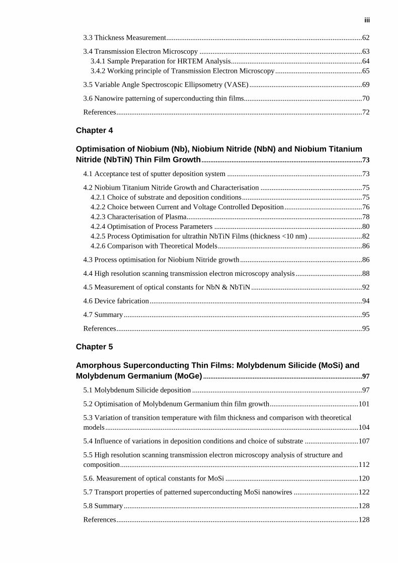
Fig. 4.11: Comparison of superconducting property of NbN films with theoretical models………86
Fig. 4.12: R versus T curve of 5.5 nm thick NbN film grown on silicon substrate………………...87
Fig. 4.13 TEM cross-section image of 6.5 nm thick NbTiN film
deposited at room temperature……………………………………………………………………..88
Fig. 4.14: Line profile analysis and thickness measurement of the room temperature deposited
NbTiN film from image shown in the Fig.4.12…………………………………………………….89
Fig. 4.15: TEM cross-section image of 6.5 nm thick NbTiN film deposited on the substrate heated
at 800°C……………………………………………………………………………………………..89
Fig. 4.16: Line profile analysis and thickness measurement of NbTiN film deposited on the heated
substrate from image shown in the Fig.4.14………………………………………………………..90
Fig. 4.17: Fast Fourier transform (FFT) view extracted from the selected area
of the TEM images…………………………………………………………………………………90
Fig. 4.18: Energy dispersive X-ray (EDX) spectrum recorded from the 6.5 nm thick NbTiN film
during HRTEM analysis……………………………………………………………………………92
Fig. 4.19: Complex refractive index measurement of 5.5 nm thick NbTiN and NbN films using
variable angle spectroscopic ellipsometry (VASE)………………………………………………...93
Fig. 4.20: Superconducting device fabrication based on the films grown following the optimised
process described in this chapter…………………………………………………………………...94
Fig. 5.1: MoSi growth optimisation………………………………………………………………...99
Fig. 5.2: R versus T curve of MoSi film with three different thicknesses deposited at room
temperature on a silicon substrate………………………………………………………………...101
Fig. 5.3: Optimisation of MoGe thin film growth………………………………………………...102
Fig. 5.4: R versus T curve of MoGe films with three different thicknesses deposited at room
temperature………………………………………………………………………………………..103
Fig. 5.5: Variation of superconducting transition temperature with film thickness & comparison
with theoretical models……………………………………………………………………………104
Fig. 5.6: Effect of substrate cooling on the superconducting transition in MoSi Films…………..108
Fig. 5.7: R(T) curve of 10 nm thick MoSi films grown on three different kinds of substrates…...109
Fig. 5.8: Large area deposition……………………………………………………………………110
Fig. 5.9: Effect of Silicon Capping Layer: Normalised Resistance versus Temperature curve of 20
nm thick MoSi films………………………………………………………………………………111
Fig. 5.10: Cross section of 5.5 thick MoSi Film without any Si cap……………………………...113
Fig. 5.11: FFT View of the selected area of the film (marked by red line in Fig. 5.10)………….113
Fig. 5.12: Line profile analysis and thickness measurement of the MoSi film
without any Si cap………………………………………………………………………………...114

xiii
Fig. 5.13: Cross section of 5.5 nm MoSi film with a Si Cap……………………………………...115
Fig. 5.14: (a): Annular dark field image of 5.5 thick MoSi film with a Si Cap (b): FFT view of the
selected area (marked by red) of the same film…………………………………………………...115
Fig. 5.15: Diffraction patterns recorded from the plan view image of 5 nm thick MoSi film
deposited on SiN membrane………………………………………………………………………116
Fig. 5.16: Speckle pattern indicating existence short or medium range order in the MoSi film….118
Fig. 5:17: Variance plot of diffracted intensity obtained from the FEM analysis of 5 nm thick MoSi
film………………………………………………………………………………………………..118
Fig. 5.18: Model of A15 crystal structure………………………………………………………...119
Fig. 5.19: Investigating the composition of uncapped co-sputtered MoSi films via Electron Energy
Loss Spectroscopy (EELS)………………………………………………………………………..120
Fig. 5.20: Complex refractive index measurement for uncapped and capped MoSi films using
variable angle spectroscopic ellipsometry (VASE) and comparison with optical constants (index of
refraction n and extinction co-efficient k) measurements of NbN and NbTiN films……………..122
Fig. 5.21: Current- Voltage curve recorded from the 390 nm wide nanowire measured at 4 K….123
Fig. 5:22: Transport measurement of nanowires patterned in a 10 nm thick MoSi thin film…….125
Fig. 5.23: Critical current density versus temperature curve of MoSi nanowires with widths ranging
from 90 nm to 2003 nm…………………………………………………………………………...127
Fig. 6.1: R(T) Curve of 90 nm thick TiN films deposited in the sputter deposited system……….133
Fig. 6.2: R(T) Curve of 30 nm thick TiN films deposited in the atomic
layer deposition system…………………………………………………………………………...135
Fig. 6.3: TEM Cross section image of 30 nm thick TiN Film deposited
in the ALD system………………………………………………………………………………...136
Fig. 6.4: Higher magnification view of the TEM Cross section image of 30 nm thick TiN Film
deposited in the ALD system……………………………………………………………………...137
Fig. 6.5: Line profile analysis and thickness measurement of TiN film deposited in ALD………137
Fig. 6.6: Structural properties of ALD deposited TiN film……………………………………….138
Fig. 6.7: TEM Cross section image of 90 nm thick TiN Film deposited in the Sputter deposition
system……………………………………………………………………………………………..139
Fig. 6.8: Line profile analysis and thickness measurement of TiN film deposited
in Sputter system………………………………………………………………………………….139
Fig. 6.9: Composition analysis of 30 nm thick TiN Film deposited in atomic layer deposition
system……………………………………………………………………………………………..140
Fig. 6.10: Design and optical microscope image of the MKID device fabricated from the 30 nm
thick ALD deposited TiN film…………………………………………………………………….141
Fig. 6.11: Low temperature characterisation of the MKID device………………………………. 142
xiv
List of Tables
Table 2.1: Superconducting materials and their respective critical temperature
in bulk form………………………………………………………………………………………...14
Table 2.2: Comparison of the superconducting properties of amorphous transition metal (TM)-
based alloy materials with conventional SNSPD material…………………………………………31
Table 3.1 Detailed Descriptions of the Sputter Targets……………………………………………52
Table 4.1: Optimised Recipe for NbTiN Deposition………………………………………………82
Table 4.2: Optimised Recipe for NbN Deposition…………………………………………………87
Table5.1 Optimised Recipe for MoSi growth…………………………………………………… 100
Table 5.2 Optimised Recipe for MoGe Growth…………………………………………………. 103
Table 5.3: Free Electron Concentration n , Ioffe-Regel parameter (kfl) and Tc of MoSi film with
four different thicknesses, d………………………………………………………………………106
Table 5.4: Superconducting Transition Temperature and RRR of 10 nm thick MoSi Film grown on
various substrates………………………………………………………………………………….108
Table 5.5: Transition Temperature (Tc), Critical Current measured at 4K ( Ic(4K)), The extracted
critical current at 0 K (Ic(0)) and Superconducting energy gap 2∆(0)………….…………………124
Table 5.6: Comparison of Critical Current density data with previous reports…………………...128
Table 6.1 Recipe used for sputtered TiN growth………………………………………………….132
Table 6.2 Recipe used for TiN growth in Atomic Layer Deposition (ALD)……………………..134

1
Chapter 1
Introduction
Single photon detection plays a significant role in a wide range of fields in science and
technology. Sensitive photon detection at the quantum level is immensely important in the
fields of quantum information processing [1], astronomy [2], remote sensing [3], deep space
communication [4] or biotechnology [5]. The detection of infrared photons also has a huge
importance in the development of next generation communication technology. On the other
hand, low noise infrared – sub millimetre wavelength photon detection has a crucial impact
on astronomical instrumentation and terahertz imaging [6], [7].
In 2001, a new single photon detector was demonstrated by Gregory Gol’tsman and his
colleagues based on superconducting niobium nitride nanowire [8]. This type of device,
known as the superconducting nanowire single-photon detector (SNSPD/SSPD), is single-
photon sensitive at visible and infrared wavelengths. The spectral range of an SNSPD
extends far into the infrared, with photon energies of just a fraction of an electron volt. Thus,
SNSPDs can operate at telecom wavelengths (1310 nm or 1550 nm) providing compatibility
with the fibre optic communications technology whereas the spectral range of traditional
semiconductor single photon detectors is limited due to the band gap of semiconductor
materials. That is why SNSPDs have been recognised as a promising technology for ultra-
weak optical signal detection. They operate at a temperature of ~4 K which is within the
reach of rapidly improving closed cycle cooling technology. Hence, the operation of
SNSPDs does not involve the use of expensive and hazardous cryogenics.
SNSPDs, nowadays, play a significant role as an enabling technology in advanced photon
counting applications. Its applications include quantum key distribution (QKD) [9], optical
quantum computing [10], characterisation of quantum emitters [11], space-to-ground
communication [12], integrated circuit testing [13], fibre sensing [14] and time-of-flight
ranging [15] etc.
The process of SNSPD fabrication starts with superconducting thin film deposition on
appropriate substrates. The quality of the superconducting films is crucial to the fabrication
of state-of-the-art SNSPDs. Understanding and controlling film quality holds the key to
realising next generation SNSPD devices like large area multipixel arrays and waveguide

2
integrated devices. DC magnetron sputtering is the most widely used technique for
depositing high quality superconducting thin films. NbN films are deposited by reactive
sputtering. The superconducting properties of NbN thin films are strongly influenced by
their crystalline structure. Their lattice constant should match well with that of the substrate
to achieve ultrathin high quality films. Thus, the crystalline nature of NbN puts a strong
constraint on the substrate choice. This problem sometimes restricts their range of
applications and potential device architectures. Polycrystalline NbTiN shows good
superconducting properties on a wider range of substrates including silicon. Recently some
research groups have started working on the possibility of SNSPD fabrication on amorphous
superconducting films (e.g. MoSi, MoGe or WSi). Amorphous films do not set strict
requirements on substrate choice as the problem of lattice matching does not arise here.
The concept of the kinetic inductance detector was first proposed by Jonas Zmuidzinas and
his group members [16]. This specific category of cryogenic detectors gained attention due
to the ability to detect photons with extreme sensitivity and suitability to multiplex in a large
array [17]. Although, initially aluminium was the conventional base material for MKIDs –
many groups have explored how various other thin films materials can be used to tune
detector properties according to specific requirements.
This thesis focuses on the growth and optimisation of superconducting thin films for next
generation superconducting detector applications.
Chapter 2 presents an in depth discussion on the various aspects of superconducting detectors
particularly in terms of thin film materials with an emphasis on SNSPDs and MKIDs. An
introductory discussion on superconductivity and superconducting materials has been
presented here. This chapter also elaborates on the theoretical models that correlate
superconducting property and materials parameters and the influence of deposition
parameters on the structural properties of superconducting thin films.
Chapter 3 describes all the experimental techniques employed for this study.
Superconducting thin films have been grown in a newly commissioned ultra-high vacuum
sputter deposition system (manufactured by Plassys Bestek, France
(http://www.plassys.com)) that is installed in the James Watt Nanofabrication Centre,
University of Glasgow. A cryogen free thin film testing station has been set up to determine
superconducting transition temperature of the films. Structural and optical properties of the
3
films have been analysed by high resolution transmission electron microscopy (HRTEM)
and variable angle spectroscopic ellipsometry (VASE).
Chapter 4 describes optimisation of Niobium (Nb), Niobium Nitride (NbN) and Niobium
Titanium Nitride (NbTiN) thin films. As a part of the acceptance test of the sputter deposition
system, the transition temperature of a 300 nm thick Nb film (9.1 K) has been reported.
NbTiN films have been grown by co-sputtering Nb and Ti in an Ar/N2 environment.
Following the optimised process, a Tc of 7.2 K has been achieved for a 5.5 nm thick NbTiN
film grown on silicon substrate. When we heat the substrate to 800°C, a NbTiN film with
the same thickness shows a transition temperature of 10.4 K. HRTEM analysis demonstrates
the polycrystalline nature of the NbTiN thin films. It also shows that substrate heating has a
positive impact on the structural property of the films.
Chapter 5 describes the growth and optimisation of amorphous MoSi and MoGe films. All
the films have been deposited by co-sputtering in an Ar environment. Variation of Tc with
film thickness and sheet resistance has been compared using theoretical models. Material
parameters extracted from the fit indicate the amorphous nature of the film. A detailed
investigation has been carried out on the local structural ordering and stoichiometry of MoSi
films using a suite of HTEM techniques. Fluctuation electron microscopy (FEM) studies
reveal that the films assumed an A15-like medium range order. Electron energy loss
spectroscopy (EELS) indicates that the film stoichiometry was close to Mo83Si17. Optical
properties from ultraviolet (270 nm) to infrared (2200 nm) wavelengths were measured via
spectroscopic ellipsometry for 5 nm thick MoSi films indicating improved long wavelength
absorption relative to NbN or NbTiN. We also measured the current density as a function of
temperature for nanowires patterned from these films. The current density at 3.6 K is 3.6 x
105A/cm2 for the widest wire studied (2003 nm), falling to 2 x 10⁵A/cm2 for the narrowest
(173 nm).
Chapter 6 describes the optimisation of TiN films by sputtering and atomic layer deposition
for microwave kinetic inductance detector (MKID) applications. For a 90 nm thick film
grown on a hydro fluoric (HF) acid cleaned silicon substrate in the sputter system, we have
obtained a Tc of 2.9 K. When we heat the substrate before deposition up to 500°C, an
improved Tc of 4 K has been achieved. A 30 nm thick TiN film grown in the ALD system
following the optimised process shows a Tc of 2.4 K.
4
Chapter 7 reviews the main advances made in this thesis and gives an outlook on future
developments.
References
[1] R. H. Hadfield, “Single-photon detectors for optical quantum information
applications,” Nat. Photonics, vol. 3, no. 12, pp. 696–705, Dec. 2009.
[2] J. M. Beckers, “Adaptive Optics for Astronomy: Principles, Performance, and
Applications,” Annu. Rev. Astron. Astrophys., vol. 31, no. 1, pp. 13–62, Sep. 1993.
[3] A. Kirmani, D. Venkatraman, D. Shin, A. Colaço, F. N. C. Wong, J. H. Shapiro, and
V. K. Goyal, “First-photon imaging.,” Science, vol. 343, no. 6166, pp. 58–61, Jan.
2014.
[4] J. A. Mendenhall, L. M. Candell, P. I. Hopman, G. Zogbi, D. M. Boroson, D. O.
Caplan, C. J. Digenis, D. R. Hearn, and R. C. Shoup, “Design of an Optical Photon
Counting Array Receiver System for Deep-Space Communications,” Proc. IEEE,
vol. 95, no. 10, pp. 2059–2069, Oct. 2007.
[5] D. Elson, J. Requejo-Isidro, I. Munro, F. Reavell, J. Siegel, K. Suhling, P. Tadrous,
R. Benninger, P. Lanigan, J. McGinty, C. Talbot, B. Treanor, S. Webb, A. Sandison,
A. Wallace, D. Davis, J. Lever, M. Neil, D. Phillips, G. Stamp, and P. French,
“Time-domain fluorescence lifetime imaging applied to biological tissue.,”
Photochem. Photobiol. Sci., vol. 3, no. 8, pp. 795–801, Aug. 2004.
[6] M. Tonouchi, “Cutting-edge terahertz technology,” Nat. Photonics, vol. 1, no. 2, pp.
97–105, Feb. 2007.
[7] G. H. Rieke, “Infrared Detector Arrays for Astronomy,” Annu. Rev. Astron.
Astrophys., vol. 45, no. 1, pp. 77–115, Sep. 2007.
[8] G. N. Gol’tsman, O. Okunev, G. Chulkova, A. Lipatov, A. Semenov, K. Smirnov,
B. Voronov, A. Dzardanov, C. Williams, and R. Sobolewski, “Picosecond
superconducting single-photon optical detector,” Appl. Phys. Lett., vol. 79, no. 6, p.
705, Aug. 2001.
[9] R. J. Collins, R. H. Hadfield, V. Fernandez, S. W. Nam, and G. S. Buller, “Low
timing jitter detector for gigahertz quantum key distribution,” Electron. Lett., vol.
43, no. 3, p. 180, Feb. 2007.
[10] J. Chen, J. Altepeter, M. Medic, K. Lee, B. Gokden, R. Hadfield, S. Nam, and P.
Kumar, “Demonstration of a Quantum Controlled-NOT Gate in the
Telecommunications Band,” Phys. Rev. Lett., vol. 100, no. 13, p. 133603, Apr.
2008.
[11] M. A. Jaspan, J. L. Habif, R. H. Hadfield, and S. W. Nam, “Heralding of
telecommunication photon pairs with a superconducting single photon detector,”
Appl. Phys. Lett., vol. 89, no. 3, p. 31112, Jul. 2006.
[12] M. E. Grein, A. J. Kerman, E. A. Dauler, O. Shatrovoy, R. J. Molnar, D. Rosenberg,
J. Yoon, C. E. DeVoe, D. V Murphy, B. S. Robinson, and D. M. Boroson, “Design
of a ground-based optical receiver for the lunar laser communications

5
demonstration,” Space Optical Systems and Applications (ICSOS), 2011
International Conference on. pp. 78–82, 2011.
[13] J. Zhang, N. Boiadjieva, G. Chulkova, H. Deslandes, G. N. Gol’tsman, A. Korneev,
P. Kouminov, M. Leibowitz, W. Lo, R. Malinsky, O. Okunev, A. Pearlman, W.
Slysz, K. Smirnov, C. Tsao, A. Verevkin, B. Voronov, K. Wilsher, and R.
Sobolewski, “Noninvasive CMOS circuit testing with NbN superconducting single-
photon detectors,” Electron. Lett., vol. 39, no. 14, p. 1086, 2003.
[14] S. D. Dyer, M. G. Tanner, B. Baek, R. H. Hadfield, and S. W. Nam, “Analysis of a
distributed fiber-optic temperature sensor using single-photon detectors.,” Opt.
Express, vol. 20, no. 4, pp. 3456–66, Feb. 2012.
[15] J. B. Abshire, H. Riris, G. Allan, X. Sun, S. R. Kawa, J. Mao, M. Stephen, E.
Wilson, and M. A. Krainak, “Laser Sounder for Global Measurement of CO 2
Concentrations in the Troposphere from Space,” in Laser Applications to Chemical,
Security and Environmental Analysis, 2008, p. LMA4.
[16] J. Zmuidzinas and P. L. Richards, “Superconducting detectors and mixers for
millimeter and submillimeter astrophysics,” Proc. IEEE, vol. 92, no. 10, pp. 1597–
1616, 2004.
[17] P. K. Day, H. G. LeDuc, B. A. Mazin, A. Vayonakis, and J. Zmuidzinas, “A
broadband superconducting detector suitable for use in large arrays,” Nature, vol.
425, no. 6960, pp. 817–821, Oct. 2003.
6
Chapter 2
Background Review
The need for efficient low noise photon detection at the infrared wavelength is gaining
importance in many fields of scientific endeavour. Single photon detectors based on
superconducting nanowires (SNSPDs) offer a promising solution for this purpose.
Microwave kinetic inductance detectors (MKIDs) are also gaining importance in the field of
low noise infrared – sub millimetre wavelength photon detection. The fabrication process of
SNSPD and MKID starts with the deposition of superconducting thin films. The growth and
optimisation of superconducting thin films for next generation superconducting detectors are
the main themes of this thesis. In this chapter, Section 2.1 presents an introduction to the
theoretical background of superconductivity. Section 2.3 presents a brief review on the
properties of superconducting thin films (including theoretical models correlating
superconducting property & materials parameters and the influence of deposition parameters
on film structures). The working principle, the main performance parameters, thin film
materials and real life applications of SNSPDs and MKIDs have been reviewed in Section
2.5 and 2.6.
2.1 Superconductivity
Superconductivity was first observed by Dutch physicist Heike Kamerling Onnes in 1911
[1], [2] and was recognised by the award of the Nobel Prize. By 1908, Onnes had succeeded
in producing liquid helium in his laboratory. Using liquid helium bath as a coolant, he
proceeded to investigate the electrical resistance of metals at low temperature. He observed
that the electrical resistance of mercury abruptly dropped to zero at 4.2 K. He reported that
below a critical temperature (specific to the material), mercury underwent a transition to a
new phase. The new phase was termed the superconducting state. Similar properties were
revealed for many more materials.
The temperature at which this phase transition occurred was termed the critical temperature
or superconducting transition temperature (Tc). It was also observed that there was a
threshold value of current density which could be carried by a superconducting material. If
the current exceeded this threshold, the material would return to the normal resistive state.
This threshold was called critical current [3]. Besides current density, applied magnetic field

7
was also observed to have a significant influence on superconductivity. Superconducting
properties would be destroyed if the applied field exceeded a threshold value. This threshold
value of the magnetic field was termed the critical field [4]. Both critical current and critical
field were function of temperature.
Fig. 2.1: The discovery of superconductivity: Resistance versus Temperature plot of
mercury when it is cooled in liquid helium bath [1].
In 1933, Walther Meissner and Robert Ochsenfeld showed that apart from the perfect
conductivity with zero resistance there was a further characteristic property of
superconducting materials [5]. They observed that when a magnetic field was applied to a
superconducting material it did not conserve magnetic field (contrary to what was expected
of a perfectly conducting material). Instead, it expelled the magnetic flux. When the applied
magnetic field was smaller than the critical field specific to the superconducting material
under observation (i.e. when the magnetic field was not large enough to destroy the
superconducting state), magnetic field density was essentially zero inside the material. Thus,
the superconducting material was seen to be perfectly diamagnetic. This effect has come to
be called the Meissner effect.
Superconducting
Transition
Zero
Resistance
R< 10-5 Ω
4.1 4.2 4.3 4.4
Temperature (K)
0.15
0.10
0.05
0
0
R (Ω)
Tc = 4.2 K
8
Due to these two unique characteristic properties (zero DC resistance and perfect
diamagnetism), superconducting materials have immense technological potential for real
world applications. Since both critical field and critical current gradually increase as the
temperature of the superconductor is further lowered below its critical temperature,
superconducting materials need to be cooled to at least around 0.6Tc (to maximize critical
current density) in most of the engineering applications. Thus, real world technological
applications of superconducting materials strongly depend on advancements in cryogenic
technology [6].
2.1.1 Theoretical Background of Superconductivity
In 1935, Fritz and Heinz London proposed a pair of simple but useful equations to describe
the electrodynamic behaviour of superconducting materials [7], [8]. Their equations are as
follows:
=∂
∂t(𝛬𝐽 ) (2.1)
And,
∇ × (𝛬𝐽 ) = −𝐵 (2.2)
[ =Applied Electric Field; 𝐽 =Superconducting Current Density; 𝛬 =𝑚𝑒
𝑛𝑒𝑒2 (me=Mass of
Electron, ne= Superconducting Electron Density and e= Electronic Charge)]
Equation (2.1) and (2.2) are called the London equations. It is to be noted that these two
equations do not explain the physical mechanism behind superconductivity. They simply
give a phenomenological description of the two characteristic properties of superconducting
materials (perfect diamagnetism and zero dc resistance) in terms of electromagnetic theory.
From Maxwell’s equations, we know that ∇ × = μo𝐽 [Since superconductors have zero
resistance we may neglect charge accumulation.]
9
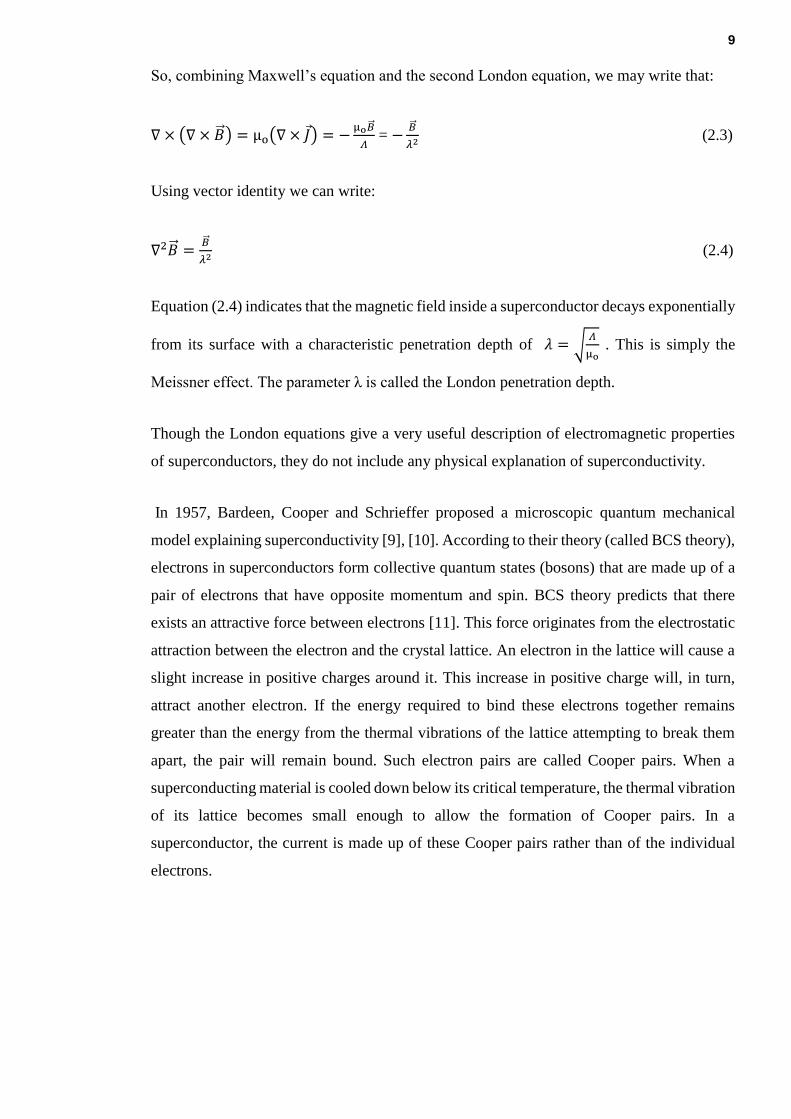
So, combining Maxwell’s equation and the second London equation, we may write that:
∇ × (∇ × ) = μo(∇ × 𝐽 ) = −μo
𝛬 = −
𝜆2 (2.3)
Using vector identity we can write:
∇2 =
𝜆2 (2.4)
Equation (2.4) indicates that the magnetic field inside a superconductor decays exponentially
from its surface with a characteristic penetration depth of 𝜆 = √𝛬
μo . This is simply the
Meissner effect. The parameter λ is called the London penetration depth.
Though the London equations give a very useful description of electromagnetic properties
of superconductors, they do not include any physical explanation of superconductivity.
In 1957, Bardeen, Cooper and Schrieffer proposed a microscopic quantum mechanical
model explaining superconductivity [9], [10]. According to their theory (called BCS theory),
electrons in superconductors form collective quantum states (bosons) that are made up of a
pair of electrons that have opposite momentum and spin. BCS theory predicts that there
exists an attractive force between electrons [11]. This force originates from the electrostatic
attraction between the electron and the crystal lattice. An electron in the lattice will cause a
slight increase in positive charges around it. This increase in positive charge will, in turn,
attract another electron. If the energy required to bind these electrons together remains
greater than the energy from the thermal vibrations of the lattice attempting to break them
apart, the pair will remain bound. Such electron pairs are called Cooper pairs. When a
superconducting material is cooled down below its critical temperature, the thermal vibration
of its lattice becomes small enough to allow the formation of Cooper pairs. In a
superconductor, the current is made up of these Cooper pairs rather than of the individual
electrons.
10
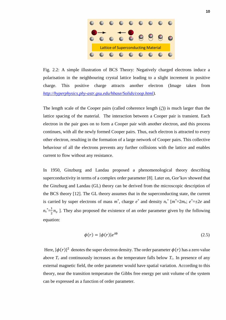
Fig. 2.2: A simple illustration of BCS Theory: Negatively charged electrons induce a
polarisation in the neighbouring crystal lattice leading to a slight increment in positive
charge. This positive charge attracts another electron (Image taken from
http://hyperphysics.phy-astr.gsu.edu/hbase/Solids/coop.html).
The length scale of the Cooper pairs (called coherence length (ξ)) is much larger than the
lattice spacing of the material. The interaction between a Cooper pair is transient. Each
electron in the pair goes on to form a Cooper pair with another electron, and this process
continues, with all the newly formed Cooper pairs. Thus, each electron is attracted to every
other electron, resulting in the formation of a large network of Cooper pairs. This collective
behaviour of all the electrons prevents any further collisions with the lattice and enables
current to flow without any resistance.
In 1950, Ginzburg and Landau proposed a phenomenological theory describing
superconductivity in terms of a complex order parameter [8]. Later on, Gor’kov showed that
the Ginzburg and Landau (GL) theory can be derived from the microscopic description of
the BCS theory [12]. The GL theory assumes that in the superconducting state, the current
is carried by super electrons of mass m*, charge e* and density ns* [m*=2me; e
*=±2e and
ns*=
1
2𝑛𝑠 ]. They also proposed the existence of an order parameter given by the following
equation:
𝜙(𝑟) = |𝜙(𝑟)|𝑒𝑖Θ (2.5)
Here, |𝜙(𝑟)|2 denotes the super electron density. The order parameter 𝜙(𝑟) has a zero value
above Tc and continuously increases as the temperature falls below Tc. In presence of any
external magnetic field, the order parameter would have spatial variation. According to this
theory, near the transition temperature the Gibbs free energy per unit volume of the system
can be expressed as a function of order parameter.
Lattice of Superconducting Material
MMaMaterial

11
According to BCS theory, electrons in the Cooper pair network are bound to each other with
energy (usually of the order of meV) specific to the material and operating temperature. This
energy is referred to as superconducting gap energy (2Δ). Whenever it is necessary to split
the Copper pairs in normal electrons to disrupt superconducting properties, it is imperative
to supply more energy than the gap energy externally. The relationship between interaction
potential of electrons and energy gap can be expressed by the following integral equation
derived from BCS theory [8]:
1
𝑁(0)𝑉𝐵𝐶𝑆= ∫
𝑡𝑎𝑛ℎ1
2𝛽(𝜉2+∆2)1/2
(𝜉2+∆2)1/2
ℏ𝜔𝑐
0 (2.6)
Here, N(0) is the density of states of electrons at absolute zero temperature, VBCS denotes the
interactional potential, 𝜔𝑐 is the cut-off frequency at which the lattice induced attraction of
the electrons is cancelled by the Coulomb potential and 𝛽 is the Boltzmann factor 1/kBT .
From this integral, temperature dependence of superconducting gap energy Δ(T) can be
computed numerically from equation (2.6) or from the approximate formula as discussed by
Khasanov et al. or Carrington et al. [13], [14] :
Δ(𝑇) = Δ(0)tanh 1.82[1.018(𝑇𝑐
𝑇− 1)]0.51 (2.7)
Dependence of critical current on temperature in the dirty limit can be described by the
following relation:
𝐼𝑐(𝑇) = 𝐼𝑐(0)∆(𝑇)
∆(0)tanh [
∆(𝑇)
2𝑘𝐵𝑇] (2.8)
Ic(T) is the critical current measured at a specific measurement temperature.
The following figure shows the temperature dependence of superconducting energy gaps of
niobium, tantalum & tin and how it matches with the numerical solution of equation (2.6) or
(2.7).
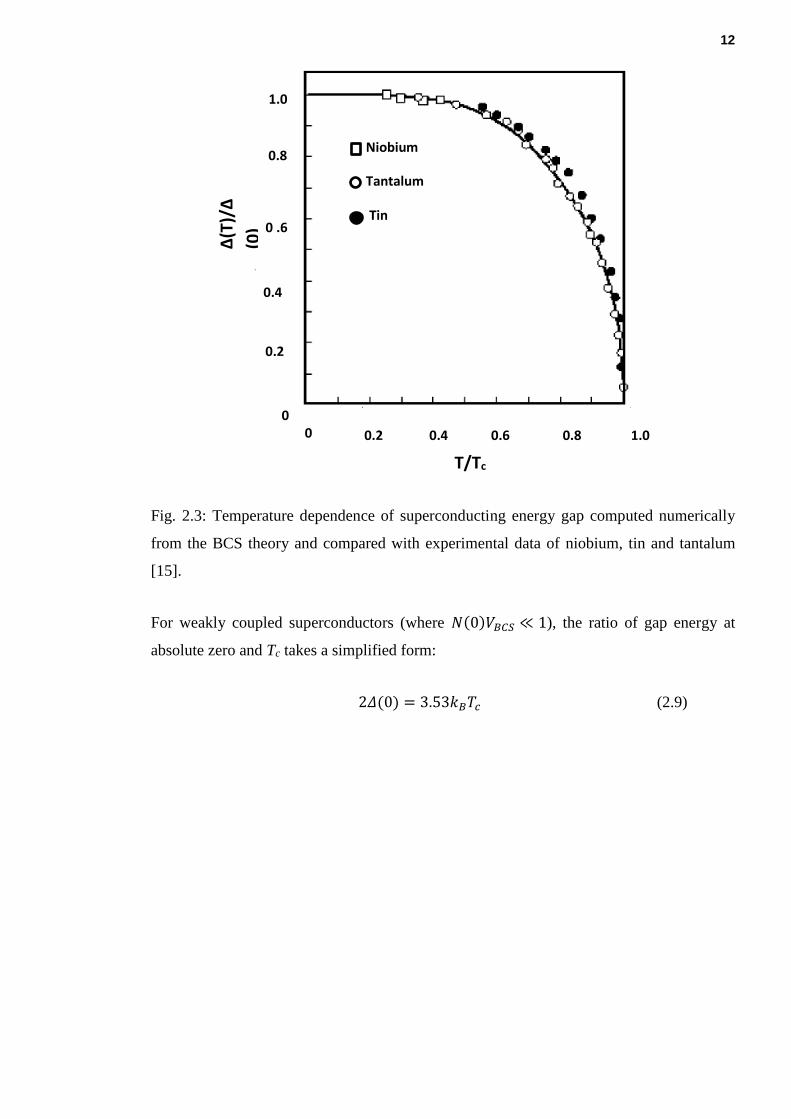
12
Fig. 2.3: Temperature dependence of superconducting energy gap computed numerically
from the BCS theory and compared with experimental data of niobium, tin and tantalum
[15].
For weakly coupled superconductors (where 𝑁(0)𝑉𝐵𝐶𝑆 ≪ 1), the ratio of gap energy at
absolute zero and Tc takes a simplified form:
2𝛥(0) = 3.53𝑘𝐵𝑇𝑐 (2.9)
0.2 0.4 0.6 0.8 1.0
1.0
0.8
0 .6
0.4
0.2
0 0
Niobium
Tantalum
Tin
T/Tc
Δ(T
)/Δ
(0)
13
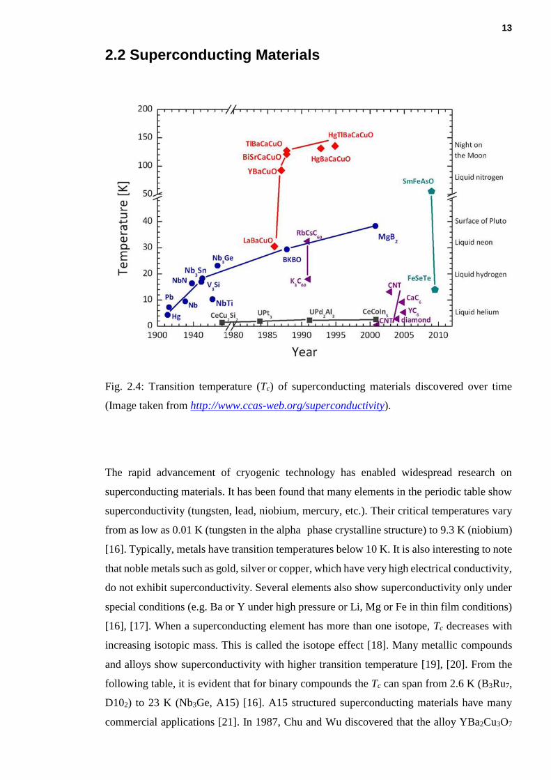
2.2 Superconducting Materials
Fig. 2.4: Transition temperature (Tc) of superconducting materials discovered over time
(Image taken from http://www.ccas-web.org/superconductivity).
The rapid advancement of cryogenic technology has enabled widespread research on
superconducting materials. It has been found that many elements in the periodic table show
superconductivity (tungsten, lead, niobium, mercury, etc.). Their critical temperatures vary
from as low as 0.01 K (tungsten in the alpha phase crystalline structure) to 9.3 K (niobium)
[16]. Typically, metals have transition temperatures below 10 K. It is also interesting to note
that noble metals such as gold, silver or copper, which have very high electrical conductivity,
do not exhibit superconductivity. Several elements also show superconductivity only under
special conditions (e.g. Ba or Y under high pressure or Li, Mg or Fe in thin film conditions)
[16], [17]. When a superconducting element has more than one isotope, Tc decreases with
increasing isotopic mass. This is called the isotope effect [18]. Many metallic compounds
and alloys show superconductivity with higher transition temperature [19], [20]. From the
following table, it is evident that for binary compounds the Tc can span from 2.6 K (B3Ru7,
D102) to 23 K (Nb3Ge, A15) [16]. A15 structured superconducting materials have many
commercial applications [21]. In 1987, Chu and Wu discovered that the alloy YBa2Cu3O7

14
has a superconducting transition temperature of 95 K which can be achieved by liquid
nitrogen [22]. Figure 2.4 illustrates the timeline of the discovery of successive classes of
superconducting materials and their transition temperatures.
Table 2.1: Superconducting materials and their respective critical temperatures in
bulk form [16]
Material Tc (K) 𝟐𝜟(𝟎) (meV)
Nb 9.1 2.77
Ti 0.4 0.12
Pb 7.2 2.19
Se 6.9 2.1
Nb3Ge 23.2 7.06
B3Ru7 2.6 0.79
MoC 14.3 4.35
VRu 5.0 1.52
MgB2 39.0 11.87
NbN 16 4.9
TiN 5 1.52
Al 1.2 0.36
YBa2Cu3O7 95.0 28.91*
(*This value has been calculated from BCS theory. High temperature superconductors have
complicated superconducting gap structure which is far from ideal BCS theory.)
2.3 Superconducting Thin Films
Thin film form of superconducting materials is the key to many nanoscale device
applications [23]. Especially in the quantum sensor based technologies, superconducting
thin films play a decisive role [24]. The relationship between low temperature and normal
state material parameters is crucial to the exploration of the superconductivity of thin films.
As is well documented in the literature, the superconducting property of thin films is tuned
with film thickness and sheet resistance [16]. (The sheet resistance of a film is defined by
𝑅𝑠 = 𝜌
𝑑 where 𝜌 is the resistivity of the film and d denotes film thickness [25].) Another
important parameter relating to the normal state and cryogenic properties of thin films is the
residual resistivity ratio (RRR). This is defined by the ratio of sheet resistance measured at
room temperature to that at 20 K [26]. It can give an idea about the metallic or insulating
15
nature of the films. It can also provide a qualitative idea about impurities or crystal defects
in the thin film. For metallic films (e.g. Nb) the higher value of RRR indicates higher metallic
purity and high crystalline structure of the film. Hence, for the metallic superconducting
materials, we should aim for high RRR values. For the semiconducting materials (e.g. NbN
and NbTiN) a RRR value >1 indicates the metallic nature of the superconducting film. On
the other hand, RRR value < 1 indicates the insulating nature.
2.3.1 Theoretical Models describing correlation of
superconductivity and material parameters of Thin Films
Reduction in the film thickness results in the degradation of superconducting property. In
particular, once the film thickness reaches a value comparable to the coherence length of the
specific material, the superconducting property of the film rapidly decreases. Since, in this
thesis, we aim to optimise ultrathin films (< 10 nm) for superconducting detectors, it is worth
exploring the theoretical models which describe the correlation between Tc, thickness and
sheet resistance and explain the thickness induced destruction of superconductivity. Several
theoretical models have been reported in the literature for this purpose [27], [28], [29].

16
Fig. 2.5: Theoretical Models describing correlation of superconductivity and material
parameters of thin films. (a) Finkel’stein Model: Comparison of the Finkel’stein model with
the Tc versus Rs data collected from a series of Mo79Ge21 samples. According to this model,
for homogeneously disordered materials suppression in Tc can be modelled as a function of
Rs (without considering thickness as a variable) [29]. (b) Simonin Model: The figure shows
how the Simonin model fits with the Tc vs d experimental measurements of niobium and
lead films. Based on Ginzburg Landau theory, this model describes the correlation between
Tc and thickness [28]. (c) Universal Scaling Law: Fitting of universal scaling law proposed
by Ivry et al. to NbN films deposited on MgO substrates. This empirical law takes into
consideration both thickness and sheet resistance dependence of superconducting properties
[27].
Finkel’stein proposed a model using renormalisation group tools [29]. This derivation was
based on a modified BCS equation. This model explains the destruction of superconductivity
through the competition between Cooper-pair attraction and disorder enhanced Coulomb
repulsion. According to this model, Tc can be expressed as a function of sheet resistance (Rs)
a) b)
c)
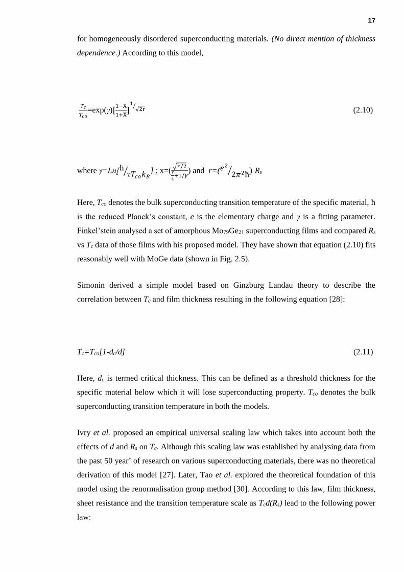
17
for homogeneously disordered superconducting materials. (No direct mention of thickness
dependence.) According to this model,
𝑇𝑐
𝑇𝑐𝑜=exp(γ)[
1−X
1+X]1
√2r⁄
(2.10)
where γ=Ln[ħ 𝜏𝑇𝑐𝑜𝑘𝐵⁄ ] ; x=(
√𝑟/2𝑟
4+1/𝛾
) and r=(𝑒2
2𝜋2ħ⁄ ) Rs
Here, Tco denotes the bulk superconducting transition temperature of the specific material, ħ
is the reduced Planck’s constant, e is the elementary charge and γ is a fitting parameter.
Finkel’stein analysed a set of amorphous Mo79Ge21 superconducting films and compared Rs
vs Tc data of those films with his proposed model. They have shown that equation (2.10) fits
reasonably well with MoGe data (shown in Fig. 2.5).
Simonin derived a simple model based on Ginzburg Landau theory to describe the
correlation between Tc and film thickness resulting in the following equation [28]:
Tc=Tco[1-dc/d] (2.11)
Here, dc is termed critical thickness. This can be defined as a threshold thickness for the
specific material below which it will lose superconducting property. Tco denotes the bulk
superconducting transition temperature in both the models.
Ivry et al. proposed an empirical universal scaling law which takes into account both the
effects of d and Rs on Tc. Although this scaling law was established by analysing data from
the past 50 year’ of research on various superconducting materials, there was no theoretical
derivation of this model [27]. Later, Tao et al. explored the theoretical foundation of this
model using the renormalisation group method [30]. According to this law, film thickness,
sheet resistance and the transition temperature scale as Tcd(Rs) lead to the following power
law:
18
Tcd=ARs-B (2.12)
Here A and B are fitting parameters. Ivry et al. discussed that the numerical value of the
exponent B can be related to structural disorder of the material. More disordered the thin
film material is higher the value of B will be.
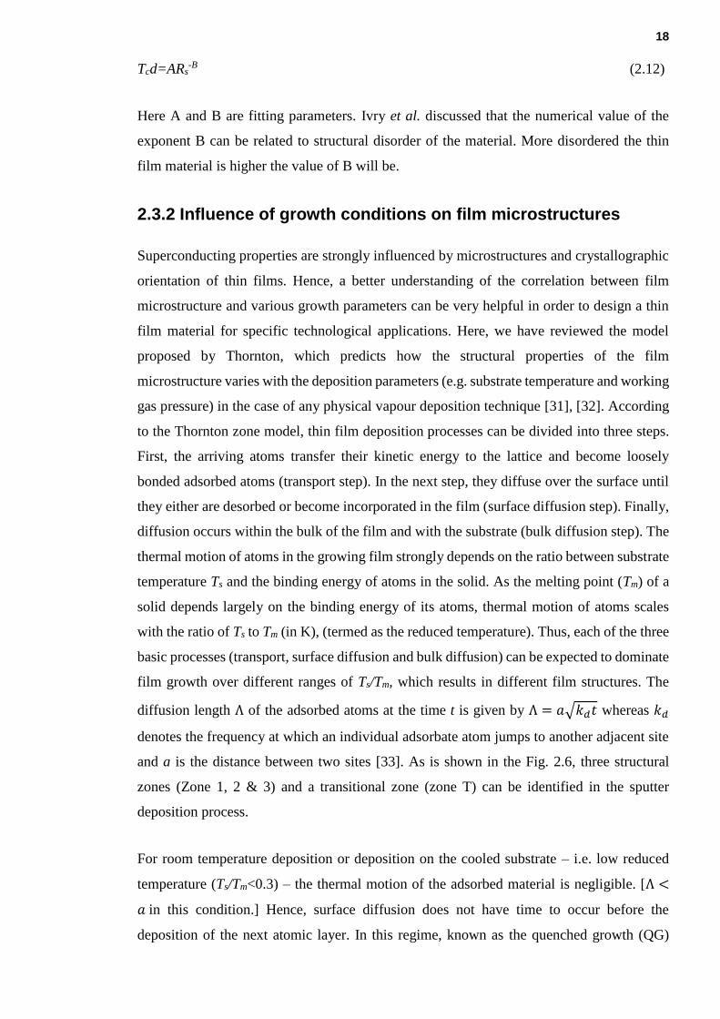
2.3.2 Influence of growth conditions on film microstructures
Superconducting properties are strongly influenced by microstructures and crystallographic
orientation of thin films. Hence, a better understanding of the correlation between film
microstructure and various growth parameters can be very helpful in order to design a thin
film material for specific technological applications. Here, we have reviewed the model
proposed by Thornton, which predicts how the structural properties of the film
microstructure varies with the deposition parameters (e.g. substrate temperature and working
gas pressure) in the case of any physical vapour deposition technique [31], [32]. According
to the Thornton zone model, thin film deposition processes can be divided into three steps.
First, the arriving atoms transfer their kinetic energy to the lattice and become loosely
bonded adsorbed atoms (transport step). In the next step, they diffuse over the surface until
they either are desorbed or become incorporated in the film (surface diffusion step). Finally,
diffusion occurs within the bulk of the film and with the substrate (bulk diffusion step). The
thermal motion of atoms in the growing film strongly depends on the ratio between substrate
temperature Ts and the binding energy of atoms in the solid. As the melting point (Tm) of a
solid depends largely on the binding energy of its atoms, thermal motion of atoms scales
with the ratio of Ts to Tm (in K), (termed as the reduced temperature). Thus, each of the three
basic processes (transport, surface diffusion and bulk diffusion) can be expected to dominate
film growth over different ranges of Ts/Tm, which results in different film structures. The
diffusion length Λ of the adsorbed atoms at the time t is given by Λ = 𝑎√𝑘𝑑𝑡 whereas 𝑘𝑑
denotes the frequency at which an individual adsorbate atom jumps to another adjacent site
and a is the distance between two sites [33]. As is shown in the Fig. 2.6, three structural
zones (Zone 1, 2 & 3) and a transitional zone (zone T) can be identified in the sputter
deposition process.
For room temperature deposition or deposition on the cooled substrate – i.e. low reduced
temperature (Ts/Tm<0.3) – the thermal motion of the adsorbed material is negligible. [Λ <
𝑎 in this condition.] Hence, surface diffusion does not have time to occur before the
deposition of the next atomic layer. In this regime, known as the quenched growth (QG)

19
regime, it is the transport process that dominates film growth, meaning that atoms become
immobilised where they land. Films resulting from these quenched growth processes exhibit
amorphous or poor crystalline microstructure (Zone 1 and zone T in Fig. 2.6):
Fig. 2.6: Influence of deposition parameters on structural properties of thin films deposited
by any physical vapour deposition technique as explained by Thornton’s structure zone
model [34].
When we start to heat the substrate during film deposition (i.e. at intermediate reduced
temperatures (0.3<Ts/Tm<0.5)), film growth gradually becomes dominated by ad-atom
surface diffusion. Films resulting from this growth regime consist of columns having tight
grain boundaries between them (Zone 2 in Fig. 2.6). Grain sizes increase with Ts/Tm. Hence,
films grown on the heated substrate have improved crystalline property in comparison to the
films grown at room temperature. If we heat substrates further to higher temperature ( i.e at
high reduced temperatures (Ts/Tm>0.5)) bulk diffusion dominates the film growth and its
structure is dominated by more isotropic and equiaxed grains (Zone 3 in Fig. 2.6 ). Zone 3
is rarely experimentally observed.
20
From the above general description of structures, it can be inferred that for amorphous films
it would be useful to grow the films at low temperatures (at room temperature or even on
cooled substrates). On the hand, for crystalline or polycrystalline materials substrate heating
would improve the structural properties of the films.
2.4 Detection of electromagnetic energy in superconductors
Due to its unique properties, superconductivity can be utilised in the detection of
electromagnetic energy. Based on Max Planck’s mathematical formulation, Einstein
postulated that electromagnetic radiation may be described as a collection of quantised
particles called photons [35], [36]. According to Planck's law, the energy of each single
photon is characterised by its frequency (E=hυ). Photon detection is immensely important in
many scientific and technological applications [37]. For instance, low energy, long
wavelength photons are particularly relevant in cosmology and astrophysics where the
Doppler shift has influenced the radiation across billions of light years [38]. In
telecommunications, fibre optic cables are used to transmit information with low attenuation
at infrared wavelength [39]. In quantum cryptography, secure cryptographic keys are created
by encoding information on the phase or polarisation of single photons [40]. Thus, infrared
photon detection is essential to the development of next generation communication
technology. Photons in the mid and far infrared are also highly relevant in the field of
atmospheric science and remote sensing [41]. In the following sections, we summarise how
superconductivity has been used to develop novel photon detection technology.
2.4.1 Superconducting Tunnel Junction
A Superconducting Tunnel Junction (STJ) consists of a thin insulating barrier layer (e.g.
Al2O3) sandwiched between two thin superconducting absorbers (e.g. Nb or Ta) [42]. When
a photon is incident on the superconducting absorber, which is maintained well below its
critical temperature (usually below 1 K), charge carriers (hot electrons) are generated as
Cooper pairs are broken. These charge carriers tunnel across the thin barrier layer resulting
in a measurable current. The magnitude of this tunnelling current depends upon the

21
tunnelling, recombination and scattering of charge carriers in the system. STJs have very
high energy resolution. For photon energies between 1 eV and 1 keV, Nb based STJ has
energy resolution between 0.13 eV and 4.3 eV full width half maximum (FWHM). Due to
their high energy resolution, STJs are of interest in the field of infrared astronomy. However,
since STJs need ultralow operational temperature and require an applied magnetic field to
suppress other tunnelling effects (Josephson current), they are too expensive and impractical
for widespread use in other applications.
Fig. 2.7: Schematic Diagram of a Superconducting Tunnel Junction (STJ): incident photons
generate quasi particles (hot electrons) in the superconducting absorber layer. They tunnel
through the insulating Al2O3 barrier to generate a measurable current signal. Tunnelling of
Cooper pairs (Josephson tunnelling) is suppressed by the application of a magnetic field
[43].
2.4.2 Superconducting Transition-Edge Sensors
A Superconducting Transition-Edge Sensor (STES) consists of a thin layer of
superconducting material (e.g. tungsten) placed on an insulating substrate. The STES
operates near the transition temperature of the superconducting thin film [44], [45]. When a
photon is incident on the sensor, the superconducting material absorbs the photon, and its
temperature slightly increases above its transition temperature. Hence, it generates a sharp
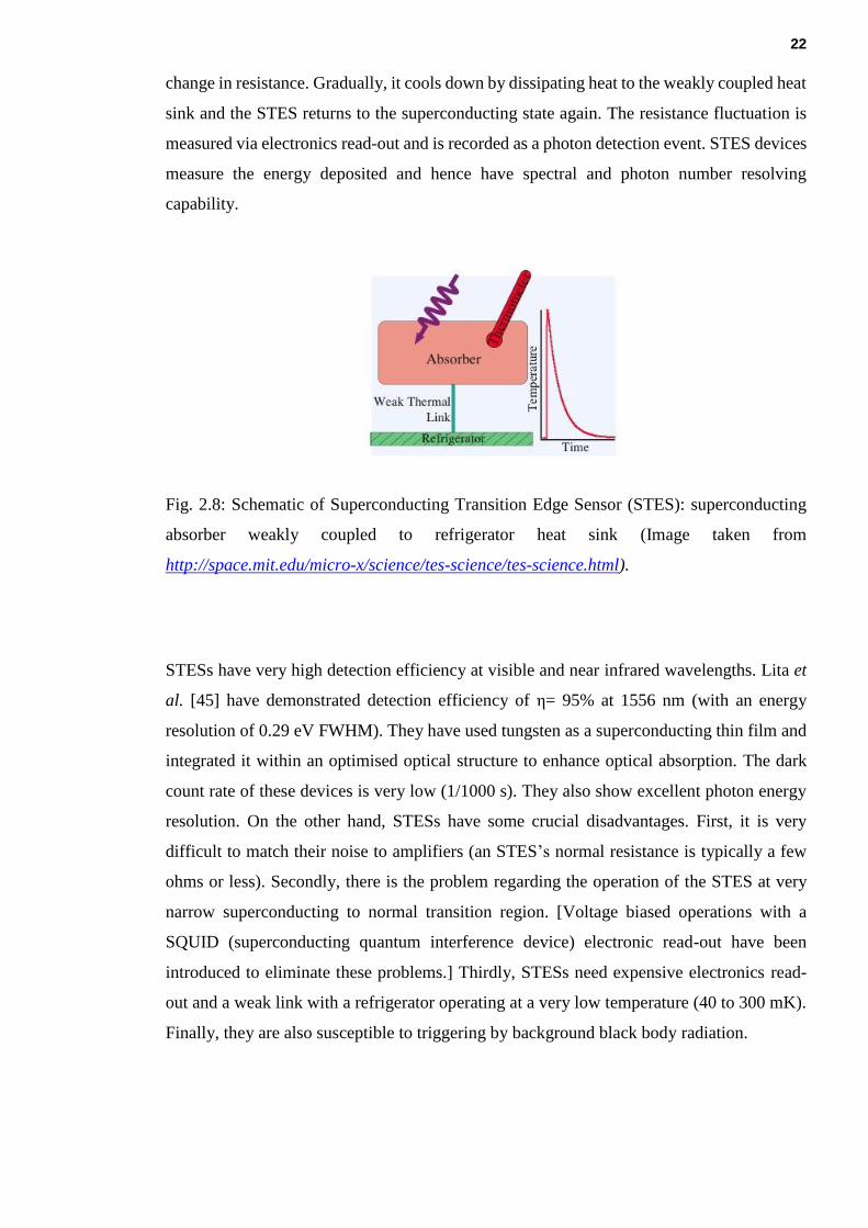
22
change in resistance. Gradually, it cools down by dissipating heat to the weakly coupled heat
sink and the STES returns to the superconducting state again. The resistance fluctuation is
measured via electronics read-out and is recorded as a photon detection event. STES devices
measure the energy deposited and hence have spectral and photon number resolving
capability.
Fig. 2.8: Schematic of Superconducting Transition Edge Sensor (STES): superconducting
absorber weakly coupled to refrigerator heat sink (Image taken from
http://space.mit.edu/micro-x/science/tes-science/tes-science.html).
STESs have very high detection efficiency at visible and near infrared wavelengths. Lita et
al. [45] have demonstrated detection efficiency of η= 95% at 1556 nm (with an energy
resolution of 0.29 eV FWHM). They have used tungsten as a superconducting thin film and
integrated it within an optimised optical structure to enhance optical absorption. The dark
count rate of these devices is very low (1/1000 s). They also show excellent photon energy
resolution. On the other hand, STESs have some crucial disadvantages. First, it is very
difficult to match their noise to amplifiers (an STES’s normal resistance is typically a few
ohms or less). Secondly, there is the problem regarding the operation of the STES at very
narrow superconducting to normal transition region. [Voltage biased operations with a
SQUID (superconducting quantum interference device) electronic read-out have been
introduced to eliminate these problems.] Thirdly, STESs need expensive electronics read-
out and a weak link with a refrigerator operating at a very low temperature (40 to 300 mK).
Finally, they are also susceptible to triggering by background black body radiation.

23
2.5 Infrared single photon detection: Superconducting Nanowire Single Photon Detector (SNSPD)
In 2001, Gol'tsman et al. first demonstrated that nano structures patterned on a
superconducting thin film may be used for single photon detection [46], [47]. They used a
bridge structure that was well below a micrometre in width and patterned via electron beam
lithography and etching in a 5 nm thick NbN superconducting film. A nanowire patterned
superconducting detector was cooled down well below its superconducting transition
temperature, and it was DC-biased with a current close to its critical current.
The nanowire absorbs incident photons depending upon the optical properties of the
superconducting material. If photons have sufficient energy (greater than the
superconducting gap energy of the material) Cooper pairs will be broken, creating hot
electrons or quasiparticles. For NbN at infrared wavelengths the absorbed photon will disrupt
hundreds of Cooper pairs in the nanowire, resulting in the formation of a resistive region as
the breaking of Cooper pairs will lead to the transition to a normal state. This small resistive
region is called a ‘hotspot’ [48]. The hotspot resistance forces the super current in the
superconducting nanowire to bypass this region. Since the width of the nanowire is very
small (~100 nm), this diversion causes the local current density around the hotspot to
increase quickly (within few picosecond) beyond the critical current density of the material,
creating a resistive barrier across the nanowire. Thus, the bias current is diverted in a parallel
path across shunt resistance [49]. As is shown in Fig. 2.10, the electrons in the hotspot region
exchange their energy with phonons in the nanowire via electron-phonon scattering with a
time a constant of 𝜏𝑒−𝑝ℎ (~ 10 ps). Then, this energy is coupled to the substrate through
phonon-phonon scattering with a time constant of 𝜏𝑝ℎ−𝑠𝑢𝑏. A small fraction of the energy
is reflected back into the electron system of the nanowire due to the lattice mismatch between
the superconducting nanowire and the substrate. Thus, the substrate (which is remained cold
at Tsubstrate) acts as a heat sink for the ‘hot’ electrons absorbing their energy [50]. In this way,
the hotspot region gradually cools down and recovers to a superconducting state and the wire
starts carrying bias currents normally. Hence, we get a measurable output voltage pulse as a
signal of the photon detection event. Recently, Engel et al. have compared the existing
theoretical descriptions of the detection mechanism of the SNSPD with the experimental
data, and they have predicted that a magnetic vortices based model may improve accuracy
of theoretical description [51].
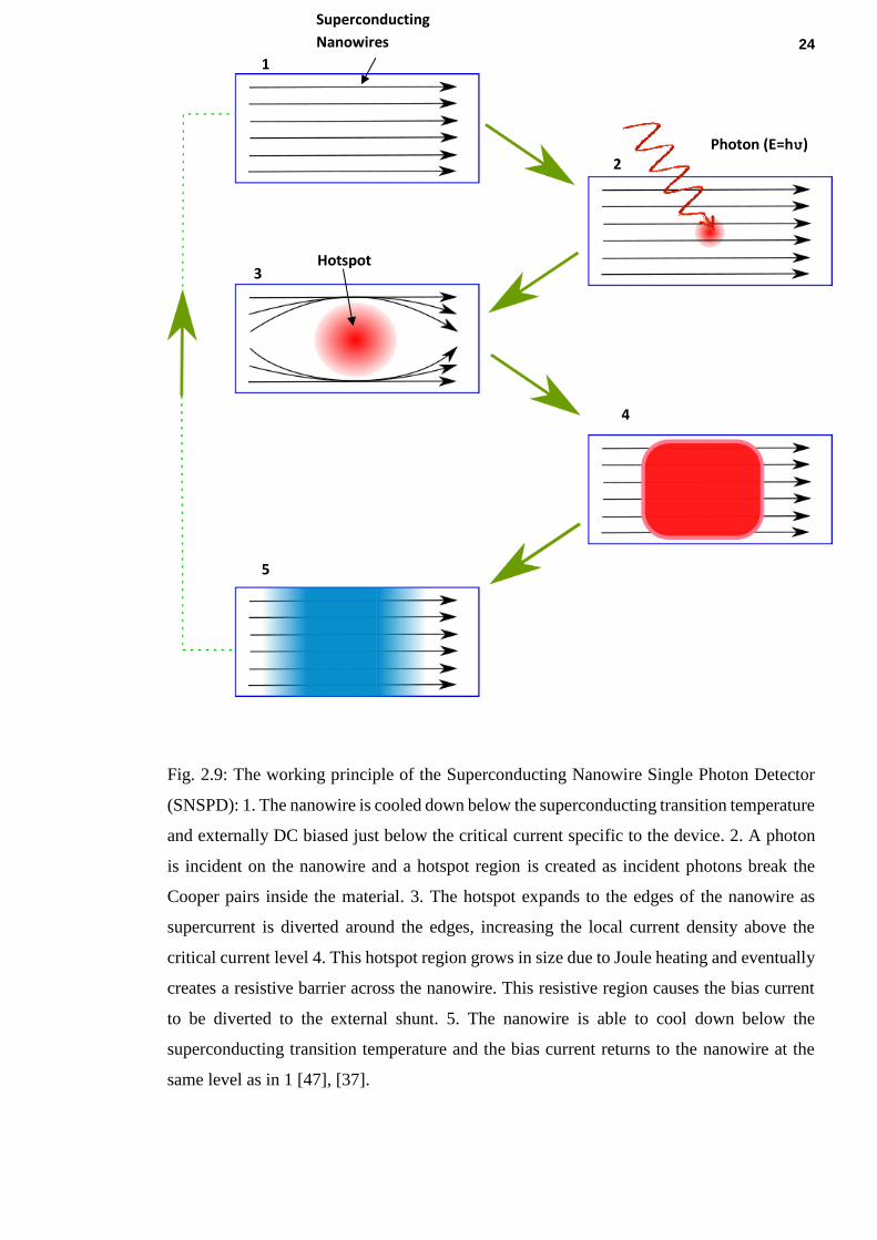
24
Fig. 2.9: The working principle of the Superconducting Nanowire Single Photon Detector
(SNSPD): 1. The nanowire is cooled down below the superconducting transition temperature
and externally DC biased just below the critical current specific to the device. 2. A photon
is incident on the nanowire and a hotspot region is created as incident photons break the
Cooper pairs inside the material. 3. The hotspot expands to the edges of the nanowire as
supercurrent is diverted around the edges, increasing the local current density above the
critical current level 4. This hotspot region grows in size due to Joule heating and eventually
creates a resistive barrier across the nanowire. This resistive region causes the bias current
to be diverted to the external shunt. 5. The nanowire is able to cool down below the
superconducting transition temperature and the bias current returns to the nanowire at the
same level as in 1 [47], [37].
2
1
3
4
5
Photon (E=hυ)
Hotspot
Superconducting
Nanowires

25
Fig. 2.10: Schematic of the energy dissipation process after photon absorption in a
superconductor: Te and Tph denote the temperature of the electron system and phonon system
of superconducting nanowires respectively. Electrons in the nanowire absorb energy from
the incident photon and a hotspot is created there (Te). The energy in the electron system is
coupled to the phonons of the superconducting material via electron-phonon scattering, with
a time constant of 𝜏𝑒−𝑝ℎ. The phonons then couple the energy to the substrate (which remains
cold at Tsubstrate ) via phonon-phonon scattering, with a time constant of 𝜏𝑝ℎ−𝑠𝑢𝑏 .
2.5.1 Performance Parameters for SNSPDs
An ideal single photon detector will generate an electrical signal whenever it absorbs a
photon. In practical scenarios, SNSPDs have non-ideal performance characteristics. The
following parameters benchmark the practical performance of SNSPD as a single photon
detector.
𝝉𝒆−𝒑𝒉
𝝉𝒑𝒉−𝒆
𝝉𝒑𝒉−𝒆

26
Fig. 2.11: An ideal single photon detector will generate a fast, well defined electrical signal
for every photon incident on it.
(a) Detection Efficiency: Detection efficiency (η) is the most crucial performance parameter
of an SNSPD. It is defined by the probability that a photon will be detected (by taking the
photon all the way through the experimental system and generating an output signal in the
read-out electronics) once a photon is incident on the detector system [52], [53]. In real life
applications, η is usually less than 100% and strongly depends on device design, uniformity
and the spectral wavelength of incident photons. Efficiency is usually measured by recording
device counts per second and comparing that to the number of incident photons.
Detection efficiency can be broken into several constituent elements. First, in any real life
application, photons can be lost before reaching the detector due to absorption, scattering or
reflection within the experimental environment. Thus, the probability of coupling incident
light with a detector is defined as the coupling efficiency (ηCoupling). Secondly, the optical
absorption property of the detector (depending on wavelength, material and geometry)
defines the number of photons which will actually be absorbed by the detector. Absorption
efficiency (ηAbsorption) gives the probability that an incident photon which is coupled with the
detector is absorbed by the SNSPD. Finally, there may be a non-unity probability that the
detector generates an output electrical signal at the read-out electronics after photon
absorption. We define this as the registering probability (ηRegistering).

27
Taking all these into account, we can write the following:
η=ηCoupling X ηAbsorption X ηRegistering (2.13)
(b) Dark Counts: An SNSPD may produce spurious signal pulses in addition to photon
detection signals due to stray light, black body radiation or electrical noise [37]. Since these
detectors are highly sensitive, they can be triggered by stray light in the experimental
environment and also by black body radiation of the experimental system. Dark counts can
be reduced by encapsulating the detectors in a radiation shield and by eliminating as much
light from the laboratory as possible. The dark count rate (DCR) is measured in terms of
counts per second (cps) or Hertz (Hz).
(c) Dead Time: During the generation of the voltage signal, superconducting nanowires are
unable to register another incoming photon [47]. This time period is known as dead time. As
discussed above, upon absorption of a photon, a small resistive hotspot is created in the
nanowire. This grows very quickly to form a resistive barrier across the wire with a time
constant of τ1. This defines the rise time of the leading edge of the output voltage pulse.
Then, the nanowire slowly cools down to a superconducting state, dissipating heat to the
substrate with a time constant of τ2. This time constant defines the trailing edge of the pulse.
The total duration of (τ1+τ2) is defined as the dead time. After this time, the detector returns
to superconducting state and becomes ready for photon detection.
(d) Timing Jitter: Timing jitter is the intrinsic timing resolution between the arrival of the
photon at the SNSPD and the generation of the output pulse [54], [55]. The jitter of a detector
is measured by calculating the Full Width at Half Maximum (FWHM) from the plot of the
statistical distribution of time delay between the arrival of a photon at the detector and the
observation of an output signal from the detector. The lower the timing jitter of a device, the
better timing precision it has for the arrival of the photon. This sets a limit on the maximum
count rate of the detector or the maximum possible clock speed that the device can be used

28
at. Low timing jitter enables high-clock-rate quantum communication experiments and leads
to improved signal-to-noise ratio (SNR) in gated photon counting experiments.
Figure of Merit: Noise equivalent power (NEP) has been widely used as a figure of merit
of photon detectors. It is measured by the input optical power, which is necessary to generate
a signal-to-noise ratio of 1 Hz output bandwidth at a given data-signaling rate or modulation
frequency, operating wavelength and effective noise bandwidth [56]. For single photon
detectors, it is given by ℎ𝜈
𝜂√2𝐷𝐶𝑅 (DCR denotes dark count of the device). However, NEP
does not take into account the timing jitter of the detector. Hadfield et al. proposed a
dimentionless figure of merit of the SNSPD considering all the perforance paramters [37].
It is defined by H=𝜂
𝐷𝐶𝑅Δ𝑡 . (Δ𝑡 denotes the timing jitter of the device.) It should be noted
that if we operate the detector at a lower bias current we will get very low dark count leading
to a low value of NEP. However, it will also reduce the detection efficiency of the device.
2.5.2 Evolution of Device Design
Since its initial demonstration, many research groups around the world have been working
to improve the performance parameters of SNSPDs. Focussing an optical spot on a ~100-
200 nm wide nanowire (well below the wavelength of infrared light) may not be feasible for
practical experiments or will lead to very poor coupling efficiency. One approach used to
solve this is to pattern the superconducting nanowire in a large square area (several microns
along each side) meander in order to increase the coupling efficiency of the incoming light.
To enhance the optical absorption in the detector, researchers have tried to integrate the
device inside an optical cavity or waveguide circuit or to deposit an anti-reflection coating
on top of the device (e.g. detectors have been fabricated on the top of SiO2/Si or
GaAs/AlGaAS distributed Bragg reflectors or Au mirrors have been used to form an optical
cavity). This reduces optical losses due to transmission or reflection from the device and
thereby increases the probability of photon absorption in the nanowire [57], [58]. Zhang et
al. have shown that a 60% system detection efficiency at a wavelength of 940 nm can be
achieved with a NbN based meander device fabricated on the top of a Si based DBR
substrate. To enhance the device’s active area so that detectors can be optically coupled
through free space or using multi-mode fibres, the concept of large area multi pixel SNSPD
array has been proposed. Allman et al. have reported the performance of free-space-coupled
64 pixel WSi based SNSPD array [59].

29
Fig. 2.12: Recent advances in SNSPD device designs from international groups (a) SNSPD
fabricated on the top of GaAS based waveguide structure to to improve optical coupling
efficency (TU Eindhoven) [60] (b) NbN based SNSPD integrated in optical cavity (MIT)
[58] (c) 64 pixel SNSPD array based on NbTiN film (NICT Japan) [61].
2.5.3 Superconducting thin films for SNSPD
The first and the most crucial step in superconducting detector fabrication is to deposit
superconducting thin film on appropriate substrates. For SNSPD operation we need ultrathin
(< 10 nm) superconducting films which can be cooled down using refrigerators. For thicker
films, the hotspot will not be able to create a resistive barrier across the nanowire. Rather, it
will decay, dissipating heat in the surroundings. Hence, the device will not be able to
generate a signal indicating photon detection. Gol’tsman et al. used 4 nm thick NbN in their
initial detectors [46]. NbN has a crucial advantage of having a comparatively higher critical
30
temperature (17 K for bulk) and shorter coherence length (~ 5 nm) [62]. Thus, it is possible
to deposit thin NbN (~ 6nm or 8nm) films which will superconduct even at 4 K [63]. Being
a very hard refractory transition metal nitride, NbN has the advantage of having stability
even over repeated thermal cycling between room temperature and cryogenic temperatures
[64]. With subsequent development, SNSPDs with NbTiN (a polycrystalline material having
properties similar to NbN) films have been evolved. NbTiN nanowire devices have been
shown to possess a shorter dead time compared to NbN devices since they have lower kinetic
inductance [65]. NbN and NbTiN have been widely employed as the base material for
SNSPD fabrication.
Since NbN or NbTiN films used in SNSPDs are very thin, the crystalline quality of the films
becomes a crucial issue. Poor crystalline quality may lead to non-uniformity in the film or
to degradation of the film's superconducting property. The lattice structure of the film
material should match well with that of the substrate to achieve ultrathin films with high
crystalline properties. Since lattice parameters of MgO (0.421 nm) [66] or sapphire (0.471
nm) [67] are very close to that of NbN (0.439 nm) [68] and NbTiN (0.434 nm) [69], these
are widely used substrates for SNSPD. Marsili et al. have reported a Tc of 8.6 K for a 3 nm
NbN film deposited on an MgO substrate [63].
However, crystalline nature of NbN & NbTiN makes substrate choice of superconducting
detectors very limited, which sometimes restricts their efficiency and range of applications.
Especially, for integration in waveguide circuits or optical cavities we need to fabricate
detectors on substrates like GaAs or silicon. Though enough research has been carried out
to heat the substrate up to a few hundred degrees centigrade during the thin film deposition
or to control film growth parameters, deposition of NbN or NbTiN on lattice mismatched
substrates or complicated optical structures is still a challenging problem [70]. Miki et al.
have demonstrated high efficiency fiber-coupled NbTiN based SNSPDs fabricated on
thermally oxidised silicon substrates (the best performing device have an SDE of 74%) [71].
Recently, several amorphous transition metal (TM) based Type II superconducting materials
(MoSi, MoGe or WSi) have been demonstrated to be highly promising alternatives for this
purpose. These materials offer various advantages to SNSPD fabrication [72]. (Type II
superconductors are a specific class of superconducting materials where there are two
differenct critical magnetic fields. At the onset of the first one, the material enter a mixed
region of normal and superconducting state, named as vortex state. At the second one,
superconducting property is completely destroyed.) They do not have strict substrate

31
requirements and also have lower superconducting gap energies which give higher intrinsic
single photon detection efficiency at long wavelengths [73]. Though they have lower critical
current density compared to NbN due to lower free carrier concentration but that also leads
to larger hotspot size during absorption of an incident photon [74].
From the eqn. 2.9 it is evident that the advantage of the lower superconducting gap (2Δ(0))
comes with a lower superconducting transition temperature. Molybdenum silicide, with a
composition of Mo75Si25, has a bulk Tc of ~7.5 K [62], which is comparatively much higher
than what other transition metal based superconducting material allows. On the other hand,
its bulk superconducting energy gap is ~ 2.28 meV [62] which is almost half of the energy
gap of NbN (4.9 meV) [73]. The following table presents a comparison between
superconducting properties of various TM based amorphous alloys and traditional SNSPD
materials. Amorphous alloys such as WSi (which is until now the most commonly used
amorphous thin film for high efficiency SNSPDs) or NbSi have very low bulk Tc. Hence, we
need an expensive and complicated cooling system to run WSi based SNSPDs below 1 K to
achieve high system detection efficiency (SDE) and low timing jitter. MoSi has a Tc > 4K
even in the thin film form although its superconducting energy gap is comparable to that of
WSi. So, it can be an ideal base material for high performance SNSPDs which can be
operated at a temperature >2K with relatively cheap, less complex closed cycle cryogenic
systems.
Table 2.2: Comparison of the superconducting properties of amorphous transition
metal (TM) based alloy materials with conventional SNSPD material
NbN MoSi MoGe WSi NbSi
Bulk Tc (K) 16 [73] 7.5 [73] 5 [62] 7.4 [62] 3.1 [75]
Thin Film
Tc (K)
8.6 (3 nm)
[63]
4.2 (4 nm)
[73]
4.4 (7.5 nm)
[62]
3.7 (4.5 nm)
[62]
2 (10 nm) [76]
Energy
Gap 2Δ(0)
(meV)
4.9 [73] 2.28 [62] 2.2 [62] 1.52 [62] 0.94
SNSPDs fabricated from WSi amorphous thin films have demonstrated better than 90%
SDE. The first MoSi based SNSPD was reported by Korneeva et al. achieving 18%
efficiency at 1200 nm wavelength [77]. Verma et al. have recently shown by integrating
32
detectors in an optical cavity, an enhanced efficiency of 87% at 1542 nm can be obtained
with 76 ps timing jitter [78].
Though high temperature superconductors (HTS) could be interesting material for SNSPDs
in terms of cryogenics, they have significant disadvantages. These materials have large
superconducting energy gaps compared to low temperature superconductors [79]. (As shown
by equation 2.9 superconducting energy gap is a linear function of Tc . Though HTSs are far
from ideal BCS superconductors its energy gap is larger due to its comparetively higher Tc
.) Hence, it is really difficult to design high efficiency SNSPDs for infrared single photon
detection based on HTS films. Ultrathin films with optimal superconducting properties based
on HTS materials are hard to produce and are subject to rapid degradation. Moreover,
complicated crystal structure and grain boundaries lead to suppresion of critical current and
formation of grain boundary based josphson junstions. It would be very challenging to
deposit uniform HTS films over a large area and fabricate nanowire based devices on them
[80].
2.5.4 Applications
SNSPDs have been demonstrated to be highly a promising alternative solution for advanced
photon counting applications. Potential applications include quantum key distribution
(QKD) [81], linear optical quantum computing [82], characterisation of quantum emitters
[83], space-to-ground communications [84], integrated circuit testing [85] and single oxygen
luminescence dosimetry for laser based cancer treatment [86]. As shown in the following
figure, the spectral sensitivity of an SNSPD covers a wide range (200 nm - >> 2µm) due to
smaller superconducting energy gap (meV instead of eV). At infrared wavelengths SNSPDs
operate with high system detection efficiency, low dark count rate and tens of picoseconds
timing jitter. On the other hand, the performance of semiconductor based single photon
detectors is restricted by material properties (e.g. for infrared photon detection SPAD
development is very complicated due to competing requirements of a material with good IR
absorption and low noise gain). Though the requirement of cryogenic operation brings
additional complexity to measurement set up, it is possible to design and fabricate high
performance SNSPDs which can be operated at a temperature >2 K using relatively cheap,
less complex closed cycle cryogenic systems. Hence, SNSPDs can be promoted as an
attractive substitute technology for single photon detection especially in the infrared spectral
domain.
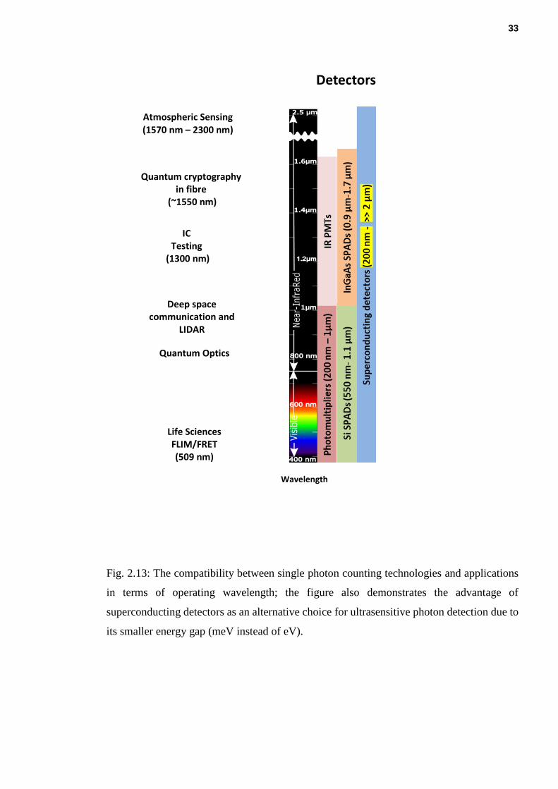
33
Fig. 2.13: The compatibility between single photon counting technologies and applications
in terms of operating wavelength; the figure also demonstrates the advantage of
superconducting detectors as an alternative choice for ultrasensitive photon detection due to
its smaller energy gap (meV instead of eV).
Detectors
Wavelength
Atmospheric Sensing (1570 nm – 2300 nm)
Quantum cryptography in fibre
(~1550 nm)
IC Testing
(1300 nm)
Life Sciences FLIM/FRET (509 nm)
Deep space communication and
LIDAR
Quantum Optics
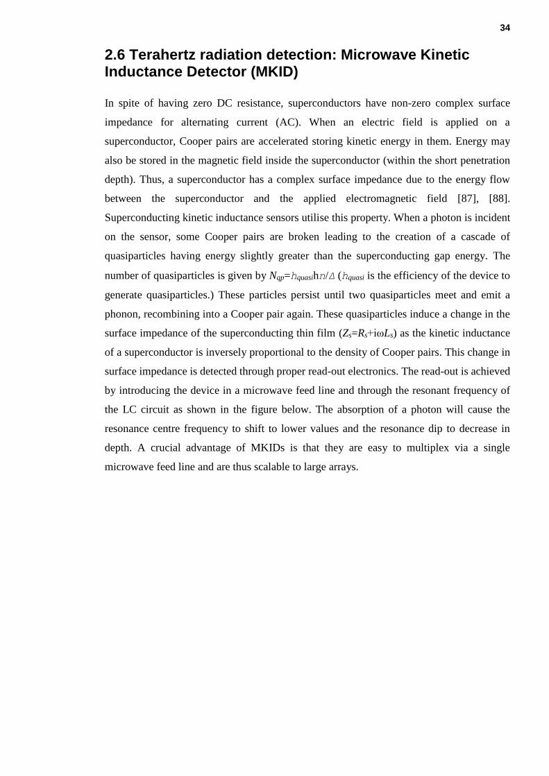
34
2.6 Terahertz radiation detection: Microwave Kinetic Inductance Detector (MKID)
In spite of having zero DC resistance, superconductors have non-zero complex surface
impedance for alternating current (AC). When an electric field is applied on a
superconductor, Cooper pairs are accelerated storing kinetic energy in them. Energy may
also be stored in the magnetic field inside the superconductor (within the short penetration
depth). Thus, a superconductor has a complex surface impedance due to the energy flow
between the superconductor and the applied electromagnetic field [87], [88].
Superconducting kinetic inductance sensors utilise this property. When a photon is incident
on the sensor, some Cooper pairs are broken leading to the creation of a cascade of
quasiparticles having energy slightly greater than the superconducting gap energy. The
number of quasiparticles is given by Nqp=hquasihn/Δ (hquasi is the efficiency of the device to
generate quasiparticles.) These particles persist until two quasiparticles meet and emit a
phonon, recombining into a Cooper pair again. These quasiparticles induce a change in the
surface impedance of the superconducting thin film (Zs=Rs+iωLs) as the kinetic inductance
of a superconductor is inversely proportional to the density of Cooper pairs. This change in
surface impedance is detected through proper read-out electronics. The read-out is achieved
by introducing the device in a microwave feed line and through the resonant frequency of
the LC circuit as shown in the figure below. The absorption of a photon will cause the
resonance centre frequency to shift to lower values and the resonance dip to decrease in
depth. A crucial advantage of MKIDs is that they are easy to multiplex via a single
microwave feed line and are thus scalable to large arrays.
35
Fig. 2.14: MKID operation principle. A: Incident photons break Cooper pairs creating
quasiparticles. B: By embedding a superconducting thin film device in a resonance circuit,
it is possible to read out changes in the complex surface impedance and frequency division
multiplexing can be achieved by coupling many resonator circuits to a single transmission
feedline. C: Measured transmission from contact 1 to 2 in resonator circuit shown in B. The
blue line represents the equilibrium situation and the red line the situation after photon
absorption [89].
2.6.1 Performance Parameters for MKIDs
Noise Equivalent Power (NEP): Noise equivalent power (NEP) is an important parameter
to measure the sensitivity of MKID detectors. In thermal equilibrium, the sensitivity of
kinetic inductance detectors is limited by the random generation and recombinations of
quasiparticles due to thermal noise. The generation-recombination noise equivalent power
NEPG-R can be expressed as [89]:
𝑁𝐸𝑃𝐺−𝑅 =2∆
𝜂𝑞𝑢𝑎𝑠𝑖√
𝑁𝑞𝑝
𝜏𝑞𝑝∝ exp (−
Δ
𝑘𝐵𝑇) (2.14)
Here, Nqp denotes the number of quasiparticles and 𝜏𝑞𝑝 is the quasiparticle life time. Since,
theoretically, both Nqp and 𝜏𝑞𝑝 follow exponential dependency with temperature, 𝑁𝐸𝑃𝐺−𝑅
also follow similar scaling with temperature. For applications in next generation far infrared
astronomoy projects , a NEP of the order of 10^-19 is required. On the other hand, for passive
teraherz imaging, a NEP ~10^-15 is sufficient [87].
36
Energy Resolution: For any photon detector which works on the concept of creation of
quasiparticles upon absorption of photons, there is a fundamental limit on the energy
resolution of the device called the Fano Limit. This limit arises because the number of
quasiparticles created by absorbing a photon is a noisy process. Due to this noise or
fluctuation, for a monochromatic incident signal, a gaussian like signal is generated instead
of a sharp delta function like peak. The full width half maximum of this peak defines the
energy resolution of the detector system. The following equation describes the energy
resolution of MKID [89]:
Δ𝐸 = 2.355√𝐸𝑝ℎ𝑜𝑡𝑜𝑛Δ𝐹𝜂𝑞𝑢𝑎𝑠𝑖−1 (2.15)
Here, F is the Fano factor and Δ denotes the energy gap. Since energy lower than this value
cannot be detected by the specific detector, the relative energy resolution is defined by,
R=E/ 𝛥𝐸 (2.16)
(E is energy of incident photons)
2.6.2 Base material for MKID
Since its first demonstration in 2003, there have been considerable research efforts made to
develop microwave kinetic inductance detectors (MKIDs). This technology is widely
employed in ground based astronomy and is under consideration for many other domains.
In the first instance, thin Al films were used to fabricate MKIDs [90]. Recently, TiN has
shown to have several advantageous properties in comparison to Al. The main benefit of
TiN thin film is its tunable superconducting property, as the Tc of the sub stoichiometric TiN
film can be tuned by changing its N2 content (in the range of 0.5 K < Tc< 5 K). Hence, we
can design the film property according to the desired frequency range to be detected or the
operating temperature of the device [91]. Also, higher room temperature resistivity of TiN
leads to higher kinetic inductance, which allows for much more straightforward and compact
designs of lumped-element MKID devices (assuming the thicknesses of the superconducting
thin films is much smaller than their London penetration depths; the correlation between
kinetic inductance and room temperature sheet resistance can be interpreted from the
following equation: 𝐿𝑘 =ℏ𝑅𝑠
𝜋Δ(0) [92]).
37
2.6.3 Application of MKIDs
MKIDs enable the detection of single photons for the frequencies ranging from infrared to
x-ray with high time resolution (~ µs) and with simultaneous energy resolution. They are
gaining importance in millimetre wave astronomy. MKIDs do not suffer from the read noise
or dark current like CCDs (charge coupled devices) or other standard detector for optical
astronomy. The following Fig. 2.15 shows an image of an IRAM 30 m telescope located in
Spain where there is an ongoing project of MKID based detector installations in this
telescope. MKIDs can also provide a low noise, high sensitivity alternative in the field of
passive terahertz imaging. There is a huge commercial market for terahertz imaging related
applications. (Applications of terahertz imaging include defence assessment, the analysis of
sub-surface features in historical art works, biomedical imaging, remote sensing in automatic
navigation systems, etc. [93], [94]) Rowe has reviewed the comparison between the key
specifications and the performance parameters of MKID based camera and other available
terahertz imaging systems [95].

38
.
Fig. 2.15: Applications of MKIDs: (a) IRAM 30 m telescope located in Spain, there is an
ongoing project of KID based detector installation (b) Passive terahertz imaging.
2.7 Summary
Detection of single photon is a crucial technology for many real life applications including
quantum information processing, astronomy, remote sensing, deep space communication or
biotechnology. Two superconducting device technologies (superconducting nanowire single
photon detectors [SSPDs/SNSPDs]) and microwave kinetic inductance detectors (MKIDs)
have the potential to outperform other existing technologies and offer scalability to large
arrays due to their unique properties. Superconducting thin films are critical for the

39
development of high efficiency superconducting detectors. In this thesis, we have studied
optimisation of NbTiN & NbN thin film growth for SNSPD fabrication. After that,
amorphous superconducting thin films have been explored (with an emphasis on MoSi) for
the same purpose. Finally, we have investigated TiN as a potential high transition
temperature base material for MKIDs for passive Terahertz imaging.
References
[1] H. Kamerlingh Onnes, “Further experiments with liquid helium. D. On the change
of electric resistance of pure metals at very low temperatures, etc. V. The
disappearance of the resistance of mercury.,” Comm. Phys. Lab. Univ. Leiden; No.
122b, 1911.
[2] D. van Delft and P. Kes, “The discovery of superconductivity,” Phys. Today, vol.
63, no. 9, pp. 38–43, Sep. 2010.
[3] D. Dew-Hughes, “The critical current of superconductors: an historical review,” vol.
27, pp. 967–979, 2001.
[4] C. Kittel, Introduction to solid state physics. Wiley, 2005.
[5] W. Meissner and R. Ochsenfeld, “Ein neuer Effekt bei Eintritt der
Supraleitfähigkeit,” Naturwissenschaften, vol. 21, no. 44, pp. 787–788, Nov. 1933.
[6] R. Radenbaugh, “Refrigeration for superconductors,” Proc. IEEE, vol. 92, no. 10,
pp. 1719–1734, Oct. 2004.
[7] F. London and H. London, “The Electromagnetic Equations of the Supraconductor,”
Proc. R. Soc. A Math. Phys. Eng. Sci., vol. 149, no. 866, pp. 71–88, Mar. 1935.
[8] M. Tinkham, Introduction to Superconductivity: Second Edition (Dover Books on
Physics) (Vol i). Dover Publications, 2004.
[9] J. Bardeen, L. N. Cooper, and J. R. Schrieffer, “Theory of Superconductivity,” Phys.
Rev., vol. 108, no. 5, pp. 1175–1204, Dec. 1957.
[10] J. Bardeen, L. Cooper, and J. Schrieffer, “Microscopic Theory of
Superconductivity,” Phys. Rev., vol. 106, no. 1, pp. 162–164, Apr. 1957.
[11] L. Cooper, “Bound Electron Pairs in a Degenerate Fermi Gas,” Phys. Rev., vol. 104,
no. 4, pp. 1189–1190, Nov. 1956.
[12] L. P. Gor ’kov, “MICROSCOPIC DERIVATION OF THE GINZBURG-LANDAU
EQUATIONS IN THE THEORY OF SUPERCONDUCTIVITY,” J. Exptl. Theor.
Phys., vol. 36, no. 36, pp. 1918–1923, 1959.
[13] R. Khasanov, P. W. Klamut, A. Shengelaya, Z. Bukowski, I. M. Savić, C. Baines,
and H. Keller, “Muon-spin rotation measurements of the penetration depth of the
Mo3 Sb7 superconductor,” Phys. Rev. B, vol. 78, p. 14502, 2008.
[14] A. Carrington and F. Manzano, “Magnetic penetration depth of MgB2,” Phys. C
Supercond., vol. 385, no. 1, pp. 205–214, 2003.
[15] F. J. Blatt, Modern physics. McGraw-Hill, 1992.

40
[16] C. P. Poole, Superconductivity. Academic Press, 2007.
[17] B. Lorenz and C. W. Chu, “High Pressure Effects on Superconductivity,” in
Frontiers in Superconducting Materials, Berlin/Heidelberg: Springer-Verlag, 2005,
pp. 459–497.
[18] J. de Launay, “The Isotope Effect in Superconductivity,” Phys. Rev., vol. 93, no. 4,
pp. 661–665, Feb. 1954.
[19] B. Matthias, T. Geballe, and V. Compton, “Superconductivity,” Rev. Mod. Phys.,
vol. 35, no. 1, pp. 1–22, Jan. 1963.
[20] T. H. Geballe, B. T. Matthias, V. B. Compton, E. Corenzwit, G. W. Hull, and L. D.
Longinotti, “Superconductivity in Binary Alloy Systems of the Rare Earths and of
Thorium with Pt-Group Metals,” Phys. Rev., vol. 137, no. 1A, pp. A119–A127, Jan.
1965.
[21] J. Muller, “A15-type superconductors,” Reports Prog. Phys., vol. 43, no. 5, pp. 641–
687, May 1980.
[22] M. Wu, J. Ashburn, C. Torng, P. Hor, R. Meng, L. Gao, Z. Huang, Y. Wang, and C.
Chu, “Superconductivity at 93 K in a new mixed-phase Y-Ba-Cu-O compound
system at ambient pressure,” Phys. Rev. Lett., vol. 58, no. 9, pp. 908–910, Mar.
1987.
[23] J. P. Pritchard, “Superconducting thin-film technology and applications,” IEEE
Spectr., vol. 3, no. 5, pp. 46–54, May 1966.
[24] T. Guruswamy, D. J. Goldie, and S. Withington, “Quasiparticle generation
efficiency in superconducting thin films,” Supercond. Sci. Technol., vol. 27, no. 5, p.
55012, May 2014.
[25] D. K. Schroder, Semiconductor material and device characterization. Wiley, 1998.
[26] N. W. Ashcroft and N. D. Mermin, Solid state physics. Brooks/Cole Cengage
Learning, 2003.
[27] Y. Ivry, C. S. Kim, A. E. Dane, D. De Fazio, A. N. McCaughan, K. A. Sunter, Q.
Zhao, and K. K. Berggren, “Universal scaling of the critical temperature for thin
films near the superconducting-to-insulating transition,” Phys. Rev. B, vol. 90, no.
21, p. 214515, 2014.
[28] J. Simonin, “Surface term in the superconductive Ginzburg-Landau free energy:
Application to thin films,” Phys. Rev. B, vol. 33, no. 11, pp. 7830–7832, Jun. 1986.
[29] A. M. Finkel’stein, “Suppression of superconductivity in homogeneously disordered
systems,” Phys. B Condens. Matter, vol. 197, no. 1, pp. 636–648, 1994.
[30] Y. Tao, “Scaling Laws for Thin Films near the Superconducting-to-Insulating
Transition,” Sci. Rep., vol. 6, no. 2, p. 23863, March. 2016.
[31] J. A. Thornton, “Influence of apparatus geometry and deposition conditions on the
structure and topography of thick sputtered coatings,” J. Vac. Sci. Technol., vol. 11,
no. 4, 1974.
[32] J. A. Thornton, “Influence of substrate temperature and deposition rate on structure
of thick sputtered Cu coatings,” J. Vac. Sci. Technol., vol. 12, no. 4, pp. 830–835,
Jul. 1975.

41
[33] D. L. Smith, Thin-film deposition : principles and practice. McGraw-Hill, 1995.
[34] F.Marsili, “Single-photon and photon-number-resolving detectors based on
superconducting nanowires,” PhD Thesis , Faculty of Science, École polytechnique
fédérale de Lausanne EPFL, Switzerland, 2009.
[35] M. Planck, “Ueber das Gesetz der Energieverteilung im Normalspectrum,” Ann.
Phys., vol. 309, no. 3, pp. 553–563, 1901.
[36] A. Einstein, “Über einen die Erzeugung und Verwandlung des Lichtes betreffenden
heuristischen Gesichtspunkt,” Ann. Phys., vol. 322, no. 6, pp. 132–148, 1905.
[37] R. H. Hadfield, “Single-photon detectors for optical quantum information
applications,” Nat. Photonics, vol. 3, no. 12, pp. 696–705, Dec. 2009.
[38] J. M. Beckers, “Adaptive Optics for Astronomy: Principles, Performance, and
Applications,” Annu. Rev. Astron. Astrophys., vol. 31, no. 1, pp. 13–62, Sep. 1993.
[39] B. Lee, “Review of the present status of optical fiber sensors,” Opt. Fiber Technol.,
vol. 9, no. 2, pp. 57–79, Apr. 2003.
[40] W. Tittel, J. Brendel, H. Zbinden, and N. Gisin, “Quantum Cryptography Using
Entangled Photons in Energy-Time Bell States,” Phys. Rev. Lett., vol. 84, no. 20, pp.
4737–4740, May 2000.
[41] A. Kirmani, D. Venkatraman, D. Shin, A. Colaço, F. N. C. Wong, J. H. Shapiro, and
V. K. Goyal, “First-photon imaging.,” Science, vol. 343, no. 6166, pp. 58–61, Jan.
2014.
[42] A. Peacock, P. Verhoeve, N. Rando, A. van Dordrecht, B. G. Taylor, C. Erd, M. A.
C. Perryman, R. Venn, J. Howlett, D. J. Goldie, J. Lumley, and M. Wallis, “Single
optical photon detection with a superconducting tunnel junction,” Nature, vol. 381,
no. 6578, pp. 135–137, May 1996.
[43] S. Friedrich, “Superconducting Tunnel Junction Photon Detectors: Theory and
Applications,” J. Low Temp. Phys., vol. 151, no. 1–2, pp. 277–286, Jan. 2008.
[44] B. Cabrera, R. M. Clarke, P. Colling, A. J. Miller, S. Nam, and R. W. Romani,
“Detection of single infrared, optical, and ultraviolet photons using superconducting
transition edge sensors,” Appl. Phys. Lett., vol. 73, no. 6, p. 735, Aug. 1998.
[45] A. E. Lita, A. J. Miller, and S. W. Nam, “Counting near-infrared single-photons
with 95% efficiency,” Opt. Express, vol. 16, no. 5, p. 3032, 2008.
[46] G. N. Gol’tsman, O. Okunev, G. Chulkova, A. Lipatov, A. Semenov, K. Smirnov,
B. Voronov, A. Dzardanov, C. Williams, and R. Sobolewski, “Picosecond
superconducting single-photon optical detector,” Appl. Phys. Lett., vol. 79, no. 6, p.
705, Aug. 2001.
[47] C. M. Natarajan, M. G. Tanner, and R. H. Hadfield, “Superconducting nanowire
single-photon detectors: physics and applications,” Supercond. Sci. Technol., vol.
25, no. 6, p. 63001, Jun. 2012.
[48] A. D. Semenov, G. N. Gol'tsman, and R. Sobolewski, “Hot-electron effect in
superconductors and its applications for radiation sensors,” Supercond. Sci.
Technol., vol. 15, no. 4, pp. R1–R16, Apr. 2002.
[49] J. K. W. Yang, A. J. Kerman, E. A. Dauler, V. Anant, K. M. Rosfjord, and K. K.

42
Berggren, “Modeling the Electrical and Thermal Response of Superconducting
Nanowire Single-Photon Detectors,” IEEE Trans. Appl. Supercond., vol. 17, no. 2,
pp. 581–585, Jun. 2007.
[50] A. J. Annunziata, “Single-Photon Detection, Kinetic Inductance, and Non-
Equilibrium Dynamics in Niobium and Niobium Nitride Superconducting
Nanowires,” PhD Thesis, Department of Physics, Yale University, U.S.A, 2010.
[51] A. Engel, J. J. Renema, K. Il ’in, and A. Semenov, “Detection mechanism of
superconducting nanowire single-photon detectors.” Supercond. Sci. Technol. , vol.
28 , no. 11, p. 114003, Sept. 2015
[52] C. Silberhorn, “Detecting quantum light,” Contemp. Phys., vol. 48, no. 3, pp. 143–
156, May 2007.
[53] S. Cova, M. Ghioni, a. Lotito, I. Rech, and F. Zappa, “Evolution and prospects for
single-photon avalanche diodes and quenching circuits,” J. Mod. Opt., vol. 51, no.
9–10, pp. 1267–1288, Jan. 2004.
[54] E. A. Dauler, B. S. Robinson, A. J. Kerman, J. K. W. Yang, E. K. M. Rosfjord, V.
Anant, B. Voronov, G. Gol’tsman, and K. K. Berggren, “Multi-Element
Superconducting Nanowire Single-Photon Detector,” IEEE Trans. Appl.
Supercond., vol. 17, no. 2, pp. 279–284, Jun. 2007.
[55] S. S. Haykin, Communication systems. Wiley, 2009.
[56] P. L. Richards, “Bolometers for infrared and millimeter waves,” J. Appl. Phys., vol.
76, no. 1, pp. 1–24, Jul. 1994.
[57] V. Anant, A. J. Kerman, E. A. Dauler, J. K. W. Yang, K. M. Rosfjord, and K. K.
Berggren, “Optical properties of superconducting nanowire single-photon
detectors,” Opt. Express, vol. 16, no. 14, p. 10750, Jul. 2008.
[58] K. M. Rosfjord, J. K. W. Yang, E. A. Dauler, A. J. Kerman, V. Anant, B. M.
Voronov, G. N. Gol’tsman, and K. K. Berggren, “Nanowire single-photon detector
with an integrated optical cavity and anti-reflection coating,” Opt. Express, vol. 14,
no. 2, p. 527, 2006.
[59] M. S. Allman, V. B. Verma, M. Stevens, T. Gerrits, R. D. Horansky, a. E. Lita, F.
Marsili, A. Beyer, M. D. Shaw, D. Kumor, R. Mirin, and S. W. Nam, “A near-
infrared 64-pixel superconducting nanowire single photon detector array with
integrated multiplexed readout,” Appl. Phys. Lett., vol. 106, no. 19, p. 192601, 2015.
[60] J. P. Sprengers, A. Gaggero, D. Sahin, S. Jahanmirinejad, G. Frucci, F. Mattioli, R.
Leoni, J. Beetz, M. Lermer, M. Kamp, S. Höfling, R. Sanjines, and A. Fiore,
“Waveguide superconducting single-photon detectors for integrated quantum
photonic circuits,” Appl. Phys. Lett., vol. 99, no. 18, p. 181110, Oct. 2011.
[61] S. Miki, T. Yamashita, Z. Wang, and H. Terai, “A 64-pixel NbTiN superconducting
nanowire single-photon detector array for spatially resolved photon detection,” Opt.
Express, vol. 22, no. 7, p. 7811, Apr. 2014.
[62] A. E. Lita, V. B. Verma, R. D. Horansky, J. M. Shainline, R. P. Mirin, and S. Nam,
“Materials Development for High Efficiency Superconducting Nanowire Single-
Photon Detectors,” MRS Proc., vol. 1807, pp. 1–6, 2015.
[63] F. Marsili, D. Bitauld, A. Fiore, A. Gaggero, F. Mattioli, R. Leoni, M. Benkahoul, F.

43
Lévy, “High efficiency NbN nanowire superconducting single photon detectors
fabricated on MgO substrates from a low temperature process.” Opt. Express, vol.
16, no. 5, p. 3191, 2008.
[64] H. O. Pierson, Handbook of refractory carbides and nitrides : properties,
characteristics, processing, and applications. Noyes Publications, 1996.
[65] S. Miki, M. Takeda, M. Fujiwara, M. Sasaki, A. Otomo, and Z. Wang,
“Superconducting NbTiN Nanowire Single Photon Detectors with Low Kinetic
Inductance,” Appl. Phys. Express, vol. 2, no. 7, p. 75002, Jun. 2009.
[66] “Magnesium oxide (MgO) crystal structure, lattice parameters, thermal expansion,”
in II-VI and I-VII Compounds; Semimagnetic Compounds, Berlin/Heidelberg:
Springer-Verlag, pp. 1–6.
[67] M. Lucht, M. Lerche, H.-C. Wille, Y. V Shvyd ’ko, H. D. Rüter, E. Gerdau, and P.
Becker, “Precise Measurement of the Lattice Parameters of Sapphire in the
Temperature Range 4.5 K -250 K Using the ossbauer Wavelength Standard,” J.
Appl. Cryst, vol. 36, no. 4, pp. 1075–1081, 2003.
[68] G. Zou, M. Jain, H. Zhou, H. Luo, S. A. Baily, L. Civale, E. Bauer, T. M.
Mccleskey, A. K. Burrell, and Q. Jia, “Ultrathin epitaxial superconducting niobium
nitride films grown by a chemical solution technique.”
[69] M. C. Burton, M. R. Beebe, K. Yang, R. A. Lukaszew, A.-M. Valente-Feliciano,
and C. Reece, “Superconducting NbTiN thin films for superconducting radio
frequency accelerator cavity applications,” J. Vac. Sci. Technol. A Vacuum,
Surfaces, Film., vol. 34, no. 2, p. 21518, Mar. 2016.
[70] F. Marsili, A. Gaggero, L. H. Li, A. Surrente, R. Leoni, F. Lévy, and A. Fiore,
“High quality superconducting NbN thin films on GaAs,” Supercond. Sci. Technol.,
vol. 22, no. 9, p. 95013, Sep. 2009.
[71] S. Miki, T. Yamashita, H. Terai, and Z. Wang, “High performance fiber-coupled
NbTiN superconducting nanowire single photon detectors with Gifford-McMahon
cryocooler.,” Opt. Express, vol. 21, no. 8, pp. 10208–14, Apr. 2013.
[72] D. Bosworth, S.-L. Sahonta, R. H. Hadfield, and Z. H. Barber, “Amorphous
Molybdenum Silicon Superconducting Thin Films,” AIP Adv., vol. 5, no. 8, p.
87106, 2015.
[73] V. B. Verma, A. E. Lita, M. R. Vissers, F. Marsili, D. P. Pappas, R. P. Mirin, and S.
W. Nam, “Superconducting nanowire single photon detectors fabricated from an
amorphous Mo0.75Ge0.25 thin film,” Appl. Phys. Lett., vol. 105, no. 2, pp. 0–5, 2014.
[74] B. Baek, A. E. Lita, V. Verma, and S. W. Nam, “Superconducting a-WxSi 1−x
nanowire single-photon detector with saturated internal quantum efficiency from
visible to 1850 nm,” Appl. Phys. Lett., vol. 98, no. 25, p. 251105, 2011.
[75] T. Proslier, J. A. Klug, J. W. Elam, H. Claus, N. G. Becker, and M. J. Pellin,
“Atomic Layer Deposition and Superconducting Properties of NbSi Films,” J. Phys.
Chem. C, vol. 115, no. 19, pp 9477–9485, May. 2011.
[76] S. N. Dorenbos, P. Forn-Díaz, T. Fuse, A. H. Verbruggen, T. Zijlstra, T. M.
Klapwijk, and V. Zwiller, “Low gap superconducting single photon detectors for
infrared sensitivity,” Appl. Phys. Lett., vol. 98, no. 25, p. 251102, June. 2011.
44
[77] Y. P. Korneeva, M. Y. Mikhailov, Y. P. Pershin, N. N. Manova, A. V Divochiy, Y.
B. Vakhtomin, A. A. Korneev, K. V Smirnov, A. G. Sivakov, A. Y. Devizenko, and
G. N. Goltsman, “Superconducting single-photon detector made of MoSi film,”
Supercond. Sci. Technol., vol. 27, no. 9, p. 95012, Sep. 2014.
[78] V. B. Verma, B. Korzh, F. Bussières, R. D. Horansky, S. D. Dyer, a E. Lita, I.
Vayshenker, F. Marsili, M. D. Shaw, H. Zbinden, R. P. Mirin, and S. W. Nam,
“High-efficiency superconducting nanowire single-photon detectors fabricated from
MoSi thin-films,” Instrum. Detect., vol. 23, no. 26, pp. 343–348, 2015.
[79] M. Hashimoto, I. M. Vishik, R.-H. He, T. P. Devereaux, and Z.-X. Shen, “Energy
gaps in high-transition-temperature cuprate superconductors,” Nat. Phys., vol. 10,
no. 7, pp. 483–495, Jun. 2014.
[80] D. M. Ginsberg, Ed., Physical properties of high temperature superconductors.
World Scientific, 1989.
[81] R. J. Collins, R. H. Hadfield, V. Fernandez, S. W. Nam, and G. S. Buller, “Low
timing jitter detector for gigahertz quantum key distribution,” Electron. Lett., vol.
43, no. 3, p. 180, Feb. 2007.
[82] E. Knill, R. Laflamme, and G. J. Milburn, “A scheme for efficient quantum
computation with linear optics.,” Nature, vol. 409, no. 6816, pp. 46–52, Jan. 2001.
[83] M. A. Jaspan, J. L. Habif, R. H. Hadfield, and S. W. Nam, “Heralding of
telecommunication photon pairs with a superconducting single photon detector,”
Appl. Phys. Lett., vol. 89, no. 3, p. 31112, Jul. 2006.
[84] M. E. Grein, A. J. Kerman, E. A. Dauler, O. Shatrovoy, R. J. Molnar, D. Rosenberg,
J. Yoon, C. E. DeVoe, D. V Murphy, B. S. Robinson, and D. M. Boroson, “Design
of a ground-based optical receiver for the lunar laser communications
demonstration,” Space Optical Systems and Applications (ICSOS), 2011
International Conference on. pp. 78–82, 2011.
[85] J. Zhang, N. Boiadjieva, G. Chulkova, H. Deslandes, G. N. Gol’tsman, A. Korneev,
P. Kouminov, M. Leibowitz, W. Lo, R. Malinsky, O. Okunev, A. Pearlman, W.
Slysz, K. Smirnov, C. Tsao, A. Verevkin, B. Voronov, K. Wilsher, and R.
Sobolewski, “Noninvasive CMOS circuit testing with NbN superconducting single-
photon detectors,” Electron. Lett., vol. 39, no. 14, p. 1086, 2003.
[86] N. R. Gemmell, A. McCarthy, B. Liu, M. G. Tanner, S. D. Dorenbos, V. Zwiller, M.
S. Patterson, G. S. Buller, B. C. Wilson, and R. H. Hadfield, “Singlet oxygen
luminescence detection with a fiber-coupled superconducting nanowire single-
photon detector,” Opt. Express, vol. 21, no. 4, p. 5005, Feb. 2013.
[87] J. Zmuidzinas and P. L. Richards, “Superconducting detectors and mixers for
millimeter and submillimeter astrophysics,” Proc. IEEE, vol. 92, no. 10, pp. 1597–
1616, 2004.
[88] B. A. Mazin, “Microwave kinetic inductance detectors,” PhD Thesis, Department of
Physcis, Mathematics and Astronomy, California Institute of Technology, U.S.A,
2005.
[89] J. Baselmans, “Kinetic Inductance Detectors,” J. Low Temp. Phys., vol. 167, no. 3–
4, pp. 292–304, Jan. 2012.
[90] B. A. Mazin, “Microwave kinetic inductance detectors: The first decade,” in AIP

45
Conference Proceedings, 2009, pp. 135–142.
[91] G. Coiffard, K.-F. Schuster, E. F. C. Driessen, S. Pignard, M. Calvo, A. Catalano, J.
Goupy, and A. Monfardini, “Uniform Non-stoichiometric Titanium Nitride Thin
Films for Improved Kinetic Inductance Detector Arrays,” J. Low Temp. Phys., vol.
184, no. 3–4, pp. 654–660, Aug. 2016.
[92] H. McCarrick, D. Flanigan, G. Jones, B. R. Johnson, P. Ade, D. Araujo, K.
Bradford, R. Cantor, G. Che, P. Day, S. Doyle, H. Leduc, M. Limon, V. Luu, P.
Mauskopf, A. Miller, T. Mroczkowski, C. Tucker, and J. Zmuidzinas, “Horn-
coupled, commercially-fabricated aluminum lumped-element kinetic inductance
detectors for millimeter wavelengths,” Rev. Sci. Instrum., vol. 85, no. 12, p. 123117,
Dec. 2014.
[93] J. F. Federici, B. Schulkin, F. Huang, D. Gary, R. Barat, F. Oliveira, and D.
Zimdars, “THz imaging and sensing for security applications?explosives, weapons
and drugs,” Semicond. Sci. Technol., vol. 20, no. 7, pp. S266–S280, Jul. 2005.
[94] J. A. Zeitler and Y.-C. Shen, “Industrial Applications of Terahertz Imaging,”
Springer Berlin Heidelberg, 2012, pp. 451–489.
[95] S. Rowe, “Passive terahertz imaging with lumped element kinetic inductance
detectors,” PhD Thesis, Department of Physics and Astronomy, School of Physics
and Astronomy, Cardiff University, U.K, 2015.

46
Chapter 3
Experimental Methods
In this chapter, we describe the experimental methods which have been employed to deposit
and characterise superconducting thin films for this study. A newly installed ultra-high
vacuum sputter deposition system has been used for the purpose of growth and process
optimisation of superconducting thin films (Section 3.1). An atomic layer deposition tool
has been used to grow TiN films (Section 3.1). Superconducting properties of the films have
been characterised in a cryogen free thin film testing set-up (Section 3.2). Structural and
optical properties have been analysed using high resolution scanning transmission electron
microscopy (Section 3.4) and variable angle spectroscopic ellipsometry (Section 3.5).
3.1 Thin Film Growth
Thin films can be grown by various techniques such as atomic layer deposition, sputtering,
electron beam evaporation, chemical vapour deposition or ion-implantation etc [1], [2].
Among these methods, sputtering is the most used technique for superconducting thin film
growth for the purpose of nanoscale device applications. Magnetron sputtering can be used
to grow all the materials we are interested in for superconducting detector fabrication, i.e.
refractory metal nitrides (NbN, NbTiN or TiN) or TM based amorphous alloys (MoSi, MoGe
or WSi). That is why we have used an ultra-high vacuum load-locked sputter deposition
system for superconducting thin film growth. The atomic layer deposition (ALD) technique
has also been explored to deposit superconducting TiN films.
3.1.1 Sputter Deposition System
A schematic of a sputter deposition process is shown in Fig. 3.1. During sputter deposition,
a high voltage is applied between the cathode (target) and anode. This ignites a glow-
discharge plasma. Positively charged plasma ions collide with the target leading to the
erosion of target particles. These target atoms are deposited on the substrate forming a thin
film. An inert gas (Ar is most widely used) is used as the medium for plasma generation. Ar+
ions have a very small mean free path (~ 52 nm under standard temperature and pressure).
So, a magnetic field across the target is maintained in order to enhance the number of high
energy ions bombarding the target. This traps secondary electrons in the discharge for a
longer duration, increasing the probability of ionising argon during their travel from cathode
to anode [3].
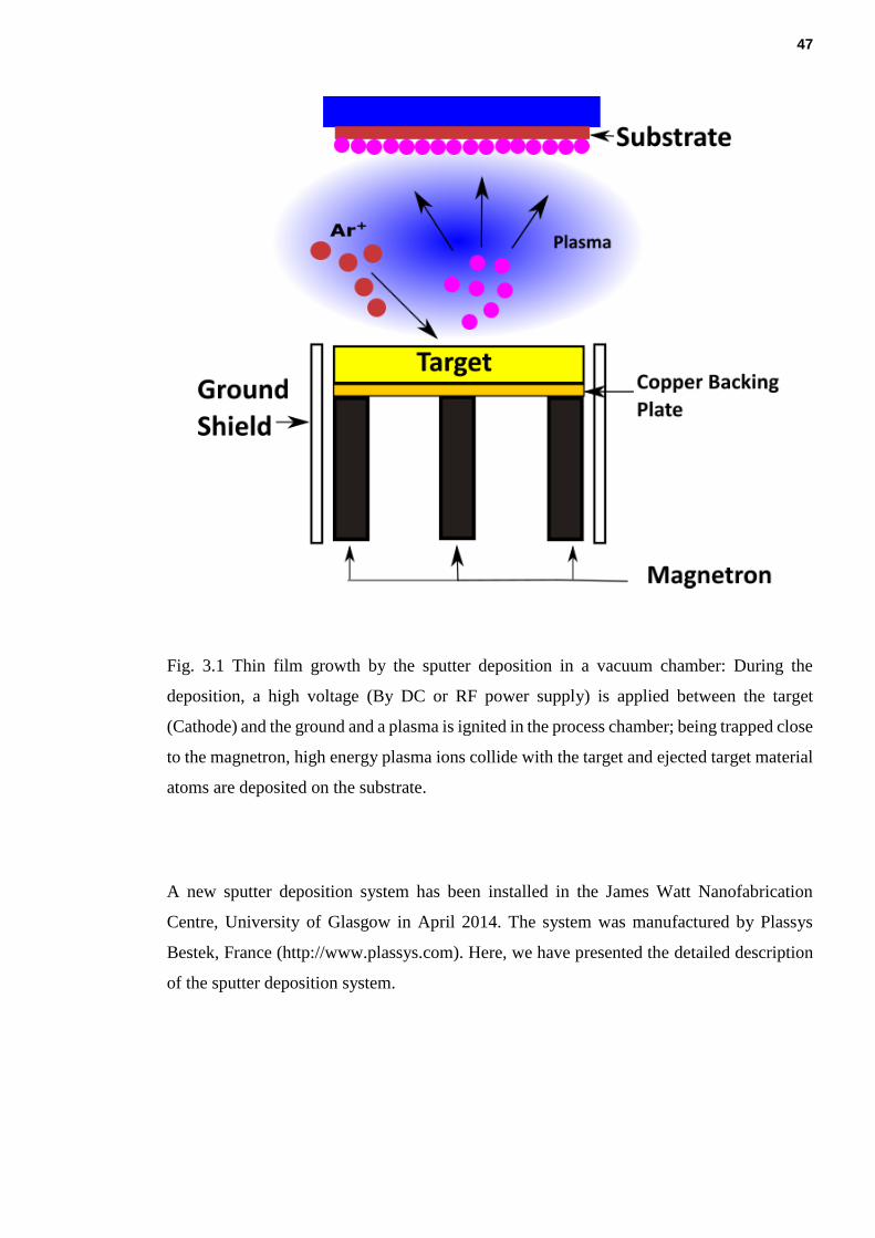
47
Fig. 3.1 Thin film growth by the sputter deposition in a vacuum chamber: During the
deposition, a high voltage (By DC or RF power supply) is applied between the target
(Cathode) and the ground and a plasma is ignited in the process chamber; being trapped close
to the magnetron, high energy plasma ions collide with the target and ejected target material
atoms are deposited on the substrate.
A new sputter deposition system has been installed in the James Watt Nanofabrication
Centre, University of Glasgow in April 2014. The system was manufactured by Plassys
Bestek, France (http://www.plassys.com). Here, we have presented the detailed description
of the sputter deposition system.

48
Fig. 3.2 Plassys VI Sputter deposition system.
Fig. 3.3 Technical drawing of the cross-section of the deposition system.
Figure 3.2 shows an image taken from the front of the system. The instrument has a 340 litre
sputtering chamber made of electro polished stainless steel. The main process chamber is
400 mm high and has an inner diameter of 600 mm. The substrate holder is attached to the
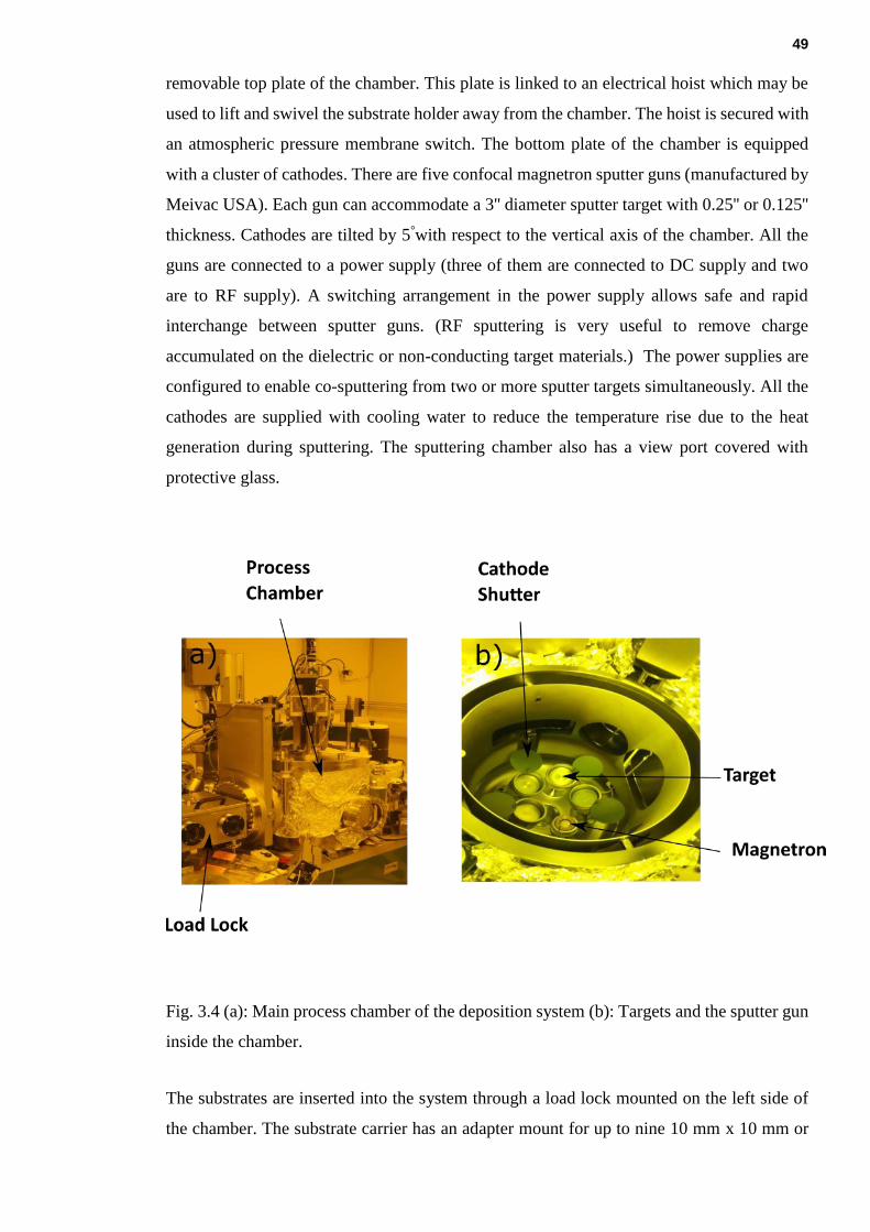
49
removable top plate of the chamber. This plate is linked to an electrical hoist which may be
used to lift and swivel the substrate holder away from the chamber. The hoist is secured with
an atmospheric pressure membrane switch. The bottom plate of the chamber is equipped
with a cluster of cathodes. There are five confocal magnetron sputter guns (manufactured by
Meivac USA). Each gun can accommodate a 3'' diameter sputter target with 0.25'' or 0.125''
thickness. Cathodes are tilted by 5°with respect to the vertical axis of the chamber. All the
guns are connected to a power supply (three of them are connected to DC supply and two
are to RF supply). A switching arrangement in the power supply allows safe and rapid
interchange between sputter guns. (RF sputtering is very useful to remove charge
accumulated on the dielectric or non-conducting target materials.) The power supplies are
configured to enable co-sputtering from two or more sputter targets simultaneously. All the
cathodes are supplied with cooling water to reduce the temperature rise due to the heat
generation during sputtering. The sputtering chamber also has a view port covered with
protective glass.
Fig. 3.4 (a): Main process chamber of the deposition system (b): Targets and the sputter gun
inside the chamber.
The substrates are inserted into the system through a load lock mounted on the left side of
the chamber. The substrate carrier has an adapter mount for up to nine 10 mm x 10 mm or
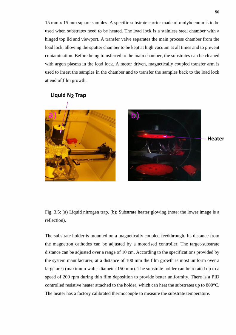
50
15 mm x 15 mm square samples. A specific substrate carrier made of molybdenum is to be
used when substrates need to be heated. The load lock is a stainless steel chamber with a
hinged top lid and viewport. A transfer valve separates the main process chamber from the
load lock, allowing the sputter chamber to be kept at high vacuum at all times and to prevent
contamination. Before being transferred to the main chamber, the substrates can be cleaned
with argon plasma in the load lock. A motor driven, magnetically coupled transfer arm is
used to insert the samples in the chamber and to transfer the samples back to the load lock
at end of film growth.
Fig. 3.5: (a) Liquid nitrogen trap. (b): Substrate heater glowing (note: the lower image is a
reflection).
The substrate holder is mounted on a magnetically coupled feedthrough. Its distance from
the magnetron cathodes can be adjusted by a motorised controller. The target-substrate
distance can be adjusted over a range of 10 cm. According to the specifications provided by
the system manufacturer, at a distance of 100 mm the film growth is most uniform over a
large area (maximum wafer diameter 150 mm). The substrate holder can be rotated up to a
speed of 200 rpm during thin film deposition to provide better uniformity. There is a PID
controlled resistive heater attached to the holder, which can heat the substrates up to 800°C.
The heater has a factory calibrated thermocouple to measure the substrate temperature.

51
Besides substrate heating, this deposition system also has the capability of cooling substrates
before film growth. The process chamber is connected to a liquid N2 trap mounted on a
flange. This trap is manually filled before film deposition. The substrate carrier is transferred
from the main chamber to an elevator mounted on the base plate. This motor driven elevator
pushes the substrate carrier against the LN2 trap to cool it down. Once the carrier has been
cooled down, it is transferred to the substrate holder. A magnetically coupled transfer arm
will move the substrate from the LN2 position to the deposition position inside the main
chamber.
The sputtering chamber is connected to two high vacuum pumping assemblies (viz. cryo and
turbo pumping system). Pumping ports are mounted on the sidewall of the chamber. They
maintain an ultra-high vacuum (with a base pressure of less than 5 X 10^-9 Torr) in the
process chamber. [Oxford Instruments model 8/8LP cryo pump, pumping speed: 1500 l/sec
for Air, 4000 l/s for H2O water cooled compressor; Edwards model STPA 803c turbo pump,
pumping speed: 800 l/sec.] The base pressure of the chamber is monitored through a hot-
filament ionisation gauge (manufactured by Kurt-J-Lesker).
The instrument is connected to four gas lines (Ar, N2, O2 and CH4). Each line is equipped
with a digitally controlled mass flow controller and a pneumatic stop valve. During the
execution of any process in the chamber, the cryo pump line is closed with a gate valve
(Mode CF 200) as reactive gases are not safe for cryo pumping and the turbo pump is
throttled with a butterfly valve (VAT model 612). The position of this throttle valve, along
with the flow rate of incoming gas, controls chamber pressure during any process.
The following table gives an overview of the sputter targets we have used for thin film
deposition in our instrument.
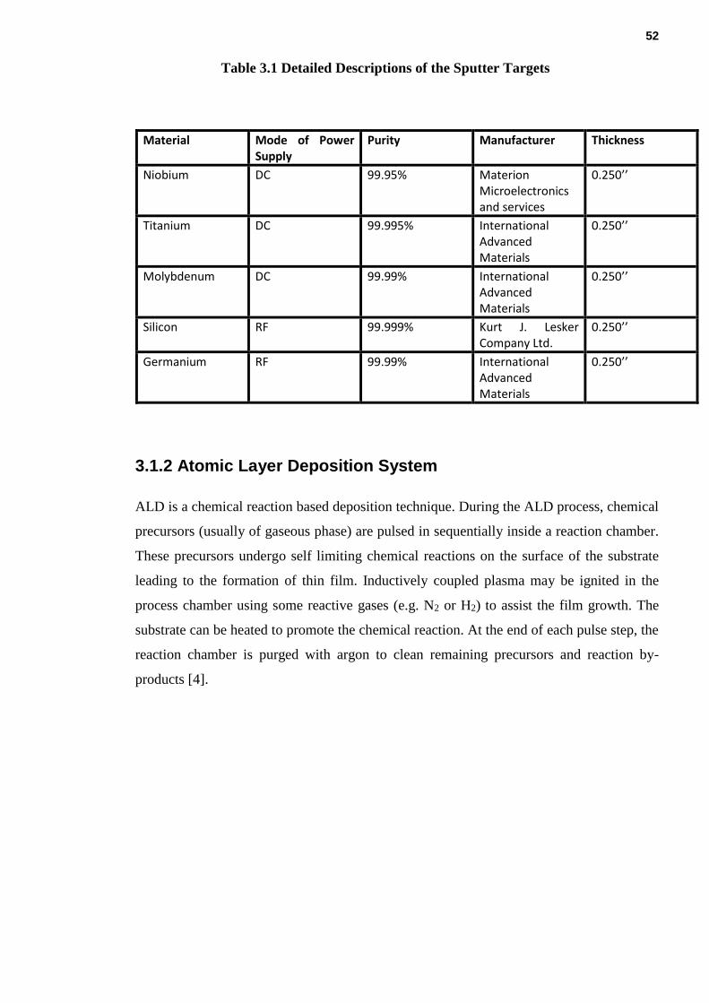
52
Table 3.1 Detailed Descriptions of the Sputter Targets
3.1.2 Atomic Layer Deposition System
ALD is a chemical reaction based deposition technique. During the ALD process, chemical
precursors (usually of gaseous phase) are pulsed in sequentially inside a reaction chamber.
These precursors undergo self limiting chemical reactions on the surface of the substrate
leading to the formation of thin film. Inductively coupled plasma may be ignited in the
process chamber using some reactive gases (e.g. N2 or H2) to assist the film growth. The
substrate can be heated to promote the chemical reaction. At the end of each pulse step, the
reaction chamber is purged with argon to clean remaining precursors and reaction by-
products [4].
Material Mode of Power Supply
Purity Manufacturer Thickness
Niobium DC 99.95% Materion Microelectronics and services
0.250’’
Titanium DC 99.995% International Advanced Materials
0.250’’
Molybdenum DC 99.99% International Advanced Materials
0.250’’
Silicon RF 99.999% Kurt J. Lesker Company Ltd.
0.250’’
Germanium RF 99.99% International Advanced Materials
0.250’’

53
Fig. 3.6: Schematic diagram of the process chamber of Atomic layer deposition (ALD):
formation of thin film by surface limiting chemical reaction on the substrate surface.
We have used a FlexAL®II ALD system manufactured by Oxford Instruments for TiN thin
film deposition. This system is integrated into a cluster tool installed in the James Watt
Nanofabrication Centre, University of Glasgow. The system can accommodate a wafer size
with a diameter of up to 200 mm (8”). There is a load lock attached to the main process
chamber, which allows substrate transfer without venting the main chamber. To increase the
efficiency of the deposition process, the wafer carrier can be electrically heated up to a
temperature of 500°C. The temperature of the substrate is monitored with the help of a PLC
controller during the deposition. The main chamber is pumped with the help of a turbo
pump. An inductively coupled plasma source (ICP 65) has been used in this system to
generate plasma during film deposition (a RF generator and AMU has served the purpose of
power supply). There is a precursor delivery module adjacent to the system to deliver
necessary precursors for the film growth. The flow of the precursors is controlled by
pneumatic valves.

54
Fig. 3.7: Atomic layer deposition chamber as a part of the cluster tool installed in the James
Watt Nanofabrication Centre, University of Glasgow, manufactured by Oxford Instruments.
3.2 Cryogen free Thin Film Testing Station1
Until the end of last century, the most common method for cooling down a superconducting
sample was to immerse it in liquid helium. Usually, liquid helium is stored in a cryogenic
storage dewar, but no dewar can provide perfect thermal insulation. Thus, the cryogenic
liquid slowly boils away and the liquid helium storage needs to be refilled regularly. This
makes the use of liquid helium dewars very expensive. Moreover, regular use of liquid
helium may lead to several safety hazards, and this demands trained personnel for proper
use. Recently developed refrigeration systems based on closed cycle cooling offer a solution
to this problem. Over the past decade, commercially available closed cycle cryo-coolers have
improved it to a large extent so far as attainable base temperature is concerned.
A closed cycle cryostat has been developed to measure the superconducting transition
temperature of the thin films. This thin film testing system is based on a Sumitomo
RDK101D coldhead and a Sumitomo CNA-11C compressor unit. The compressor and the
coldhead are connected with a two way gas line. This system runs through a 13 A electrical
outlet (with 1 kW power consumption) and requires only air cooling. The operation of this
cold head is based on Gifford-McMahon (GM) closed cycle cooling. High purity helium is
1 The cryogen-free thin film testing set up was designed by the author and built up by Kleanthis
Erotokritou as a part of his master thesis.

55
circulated through the cold head and compressor. The cyclic operation of the GM cryo-
cooler consists of 4 steps [5].
Step 1: At first, the high pressure inlet valve is open. The displacer is moved to the top of
the coldhead. The gas flows through the regenerator to the bottom of the coldhead. The
regenerator absorbs heat from the gas, reducing its temperature. This gas, in turn, reduces
the temperature of the coldhead.
Step 2: The high pressure valve is then closed and the low pressure valve is opened with the
position of the displacer fixed at the top. Part of the gas flows through the regenerator to the
low pressure side of the compressor. Thus, gas in the cold head expands. This expansion
cools down the gas further.
Step 3: The displacer is moved to the bottom of the coldhead forcefully (using a motor).
This forces the cold gas to pass the regenerator while taking up heat from the regenerator.
Gas flows to the low pressure outlet valve.
Step 4: The outlet valve is then closed and the inlet valve is opened with the displacer at a
fixed position. The gas, now in the hot end of the coldhead, is compressed and heat is
released to the surroundings. At the end of this step, we are back to Step 1.
Sub-helium temperature can easily be achieved by building multi stage cryo-coolers. As
shown in the following figure, the coldhead we have used has two stages: One warmer stage
and another colder stage which reach a base temperature of ~3-4K during cool-down.
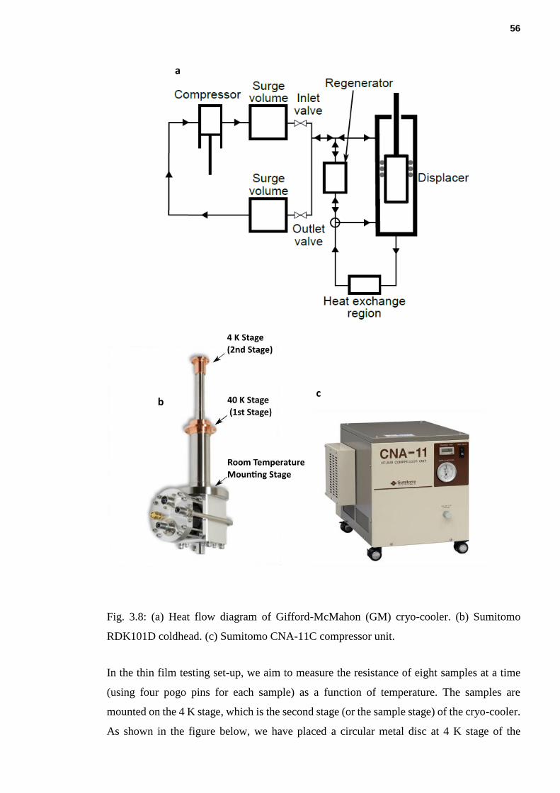
56
Fig. 3.8: (a) Heat flow diagram of Gifford-McMahon (GM) cryo-cooler. (b) Sumitomo
RDK101D coldhead. (c) Sumitomo CNA-11C compressor unit.
In the thin film testing set-up, we aim to measure the resistance of eight samples at a time
(using four pogo pins for each sample) as a function of temperature. The samples are
mounted on the 4 K stage, which is the second stage (or the sample stage) of the cryo-cooler.
As shown in the figure below, we have placed a circular metal disc at 4 K stage of the
a
b c

57
coldhead. Around this disc there are 8 rectangular holes with steps at their boundary to place
pogo pin holders (as shown in Figure 3.10(a)). In each holder (made of Tufnol laminated
plastic) we have inserted four pogo pins by press fitting. On the top of this, we placed another
circular metal disc. This disc has eight slots to accommodate eight 15 mm x 15 mm square
samples (Figure 3.10(b)). Our samples (thin films sputtered on different substrates) are to be
placed in these slots. An insulating carrier is used for this purpose to avoid shortage between
the edge of samples and the metal stage. This disc is to be placed on the metal stage with
pogo pins in such a way that all the pogo pins can touch the samples. Oxygen-Free High
Conductivity (OFHC) copper has been used for these metallic parts as it has a very high
thermal conductivity.
Fig. 3.9: Block diagram of the cryogen free thin film testing set up.

58
The coldhead needs to be encapsulated in a vacuum can and sealed off before cool-down
because cold surfaces act as a trap for any residual gases remaining inside the chamber after
the cool-down, and this can lead to a serious hazard. We have attached a hexagonal base at
the bottom of the cold head (Fig. 3.10 (c)). A vacuum can with commercially available O-
rings and flanges have been placed over the hexagonal base. Before every cool-down, the
system has been pumped down and sealed off using an isolation valve.
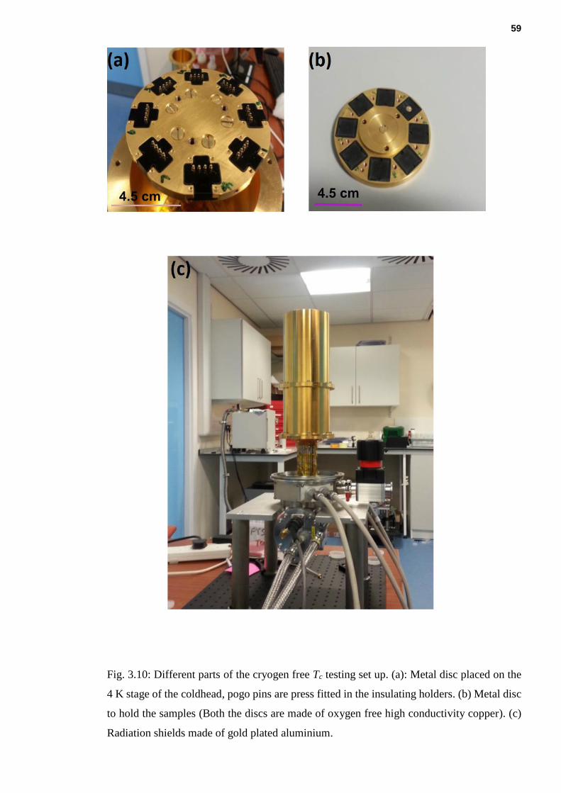
59
Fig. 3.10: Different parts of the cryogen free Tc testing set up. (a): Metal disc placed on the
4 K stage of the coldhead, pogo pins are press fitted in the insulating holders. (b) Metal disc
to hold the samples (Both the discs are made of oxygen free high conductivity copper). (c)
Radiation shields made of gold plated aluminium.

60
One of the primary requirements for our cryostat design is to reach a stable base temperature
of below 4 K for a long period of time so that it can be employed in the electrical
characterisation of superconducting thin films. For that purpose, it is necessary to reduce the
heat load in the cryostat as much as possible. Radiative heat load can be a significant problem
in reaching very low temperatures due to the huge difference between ambient temperature
and temperature in the coldhead. Therefore, we have mounted a radiation shield on the 40 K
stage of the cold head. Metals with highly reflective surfaces can be used for this purpose
since these have very low radiation emissivity. Emissivity can be further reduced by
polishing the metals’ surfaces. We have used gold plated aluminium for the radiation shield.
For the electronics read-out we have used an isolated voltage source (SRS SIM928) in series
with a resistor to provide a constant amount of current through the outer pair of pogo pins at
each individual sample. At the same time, we have measured the voltage difference across
each sample with the help of an inner pair of pins as a function of cryostat temperature (four
point resistance measurement). We have introduced a programmable Labjack switch which
is connected to a computer through a RS-232 cable. The purpose of the Labjack is to record
the applied current and measure potential difference values across each sample and then
calculate their individual resistance by the use of a home built Python program. Additionally,
an electronic switching circuit (relay) is connected through the Labjack to the computer in
order to swap between the connected samples. The isolated voltage source, digital voltmeter
and temperature sensors are installed in an SRS SIM900 mainframe.
For temperature measurement, we have used a silicon diode thermometer manufactured by
Lake Shore which can be used in a cryogenic environment. The thermometer is attached to
the 4 K stage of the coldhead. Since the accuracy of temperature measurement is crucial for
this set-up, this thermometer is individually calibrated by the manufacturing company. It is
calibrated from 1.4 K to 325 K with a tolerance of ±12 mK. The calibrated curve has been
loaded to the SRS temperature sensor by a Python program. In order to connect the pogo
pins of each sample to the electronic controlling circuit, we have used twisted pairs of a 110
micrometre diameter polyester insulated constantan wire. This wire was chosen mainly due
to the fact that low thermal conductivity of constantan would help to decrease conductive
heat load on the system. These wires connect the pogo pins and the hermetically sealed
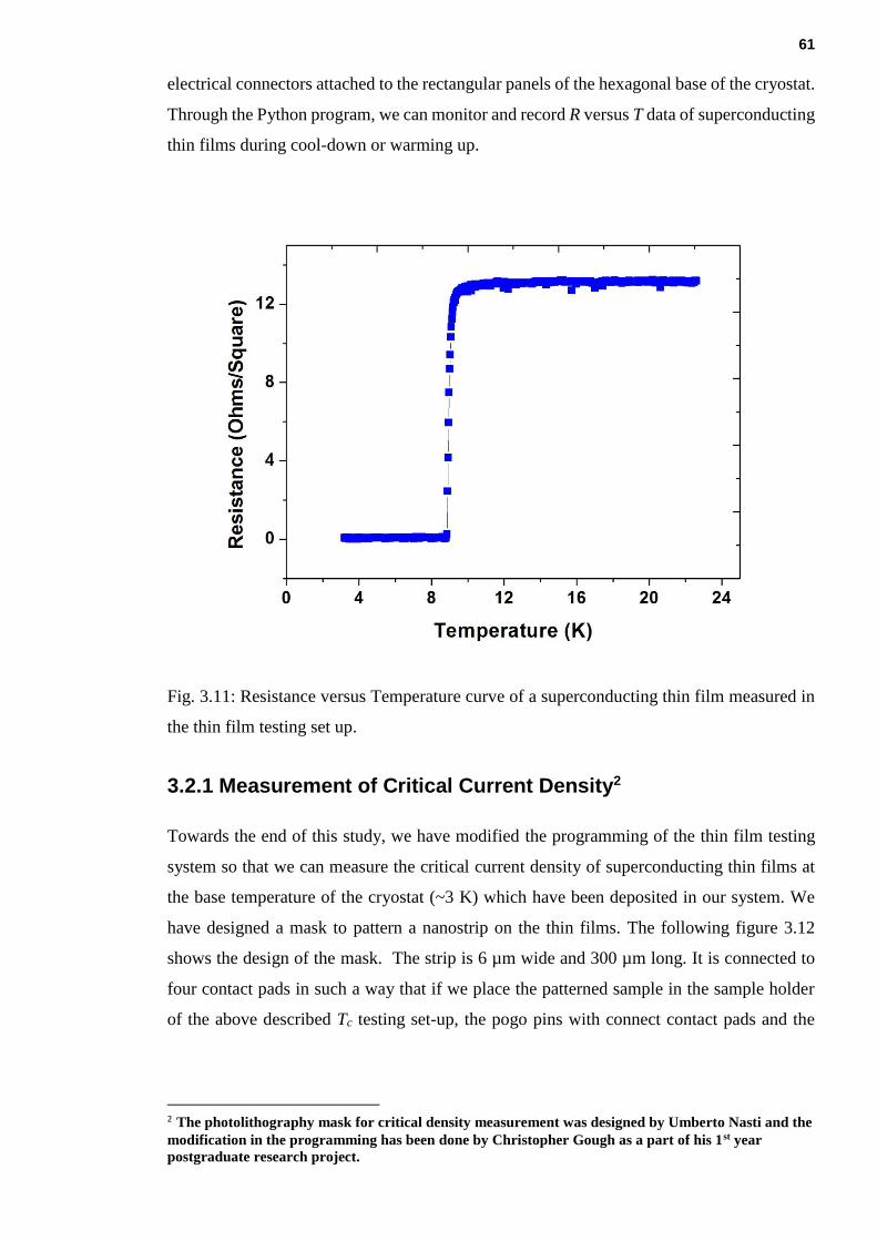
61
electrical connectors attached to the rectangular panels of the hexagonal base of the cryostat.
Through the Python program, we can monitor and record R versus T data of superconducting
thin films during cool-down or warming up.
Fig. 3.11: Resistance versus Temperature curve of a superconducting thin film measured in
the thin film testing set up.
3.2.1 Measurement of Critical Current Density2
Towards the end of this study, we have modified the programming of the thin film testing
system so that we can measure the critical current density of superconducting thin films at
the base temperature of the cryostat (~3 K) which have been deposited in our system. We
have designed a mask to pattern a nanostrip on the thin films. The following figure 3.12
shows the design of the mask. The strip is 6 µm wide and 300 µm long. It is connected to
four contact pads in such a way that if we place the patterned sample in the sample holder
of the above described Tc testing set-up, the pogo pins with connect contact pads and the
2 The photolithography mask for critical density measurement was designed by Umberto Nasti and the
modification in the programming has been done by Christopher Gough as a part of his 1st year
postgraduate research project.
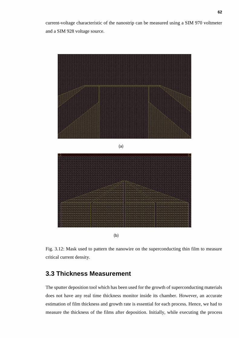
62
current-voltage characteristic of the nanostrip can be measured using a SIM 970 voltmeter
and a SIM 928 voltage source.
(a)
(b)
Fig. 3.12: Mask used to pattern the nanowire on the superconducting thin film to measure
critical current density.
3.3 Thickness Measurement
The sputter deposition tool which has been used for the growth of superconducting materials
does not have any real time thickness monitor inside its chamber. However, an accurate
estimation of film thickness and growth rate is essential for each process. Hence, we had to
measure the thickness of the films after deposition. Initially, while executing the process

63
optimisation for different materials, we followed a simple process to measure thickness.
Before deposition, we drew a line across the substrate with an ink gel pen. After that, the
substrate is inserted into the chamber and film is deposited on the top of it. At the end of
deposition cycle, we etched the ink with acetone. Finally, the step created in the etch process
can be scanned in atomic force microscopy (AFM). From this AFM scan, we can measure
the thickness of the film.
Later on, several films have been analysed in high resolution transmission electron
microscopy (HRTEM) and variable angle spectroscopic ellipsometry (VASE). We have
extracted film thickness from these techniques and compared it with AFM measurements.
Fig. 3.13: Thickness measurement: (a) Step created by making a cross mark on the substrate
with help of an ink pen prior to film growth and etching the film in acetone after deposition.
(b) AFM scan across the step created. (c) Thickness measurement from the step profile.
3.4 Transmission Electron Microscopy3
We have analysed chemical composition and structural characteristics of superconducting
thin films in high resolution transmission electron microscopy (HRTEM). The transmission
electron microscope facilities available in the School of Physics and Astronomy, University
of Glasgow (JEOL ARM200cF and FEI Tecnai T20 microscope) have been used for this
3 Transmission electron microscopy analysis has been carried out in collaboration with the research
group led by Dr. Ian MacLaren, School of Physics and Astronomy, University of Glasgow.

64
purpose. Before the HRTEM analysis, electron transparent cross sections have been prepared
using a dual beam focussed ion beam (FIB) system [6].
3.4.1 Sample Preparation for HRTEM Analysis
At the beginning of the sample preparation, a conductive layer is deposited on the top of the
film as a protection against the potential damage during FIB processing. For our samples,
Gold has been used as the protective layer. After that, the sample is inserted in the FIB
system. A metal strip (Pt for our films) is deposited on the region of interest using ion beam
(Fig. 3.14 (b)). Then, material surrounding the region of interest is removed with the help of
a focussed ion beam. As shown in Fig. 3.14 (c), a large stair-step FIB trench is cut on one
side of the area of interest and a rectangular trench is made on the other side. After this
step, the sample holder is tilted to an angle of >45° and then the bottom, left side and a
portion of the right side of the specimen is cut so that the sample is partially released. Then,
the holder is tilted back to its original position and the specimen is thinned to electron
transparency. For HRTEM analysis, a final thinning is performed at an angle of ∼1–2° with
respect to the plane of the sample surface. The thinnest portion of the sample lies in the area
of interest for HRTEM analysis (usually ~50 nm). Finally, a micromanipulator is used to
lift the sample cross section from the trench and transfer to a copper TEM mesh grid (Fig.
3.14 (d)).
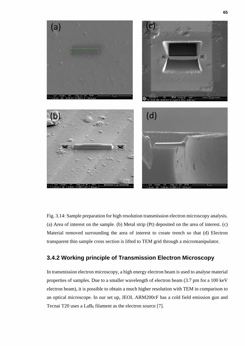
65
Fig. 3.14: Sample preparation for high resolution transmission electron microscopy analysis.
(a) Area of interest on the sample. (b) Metal strip (Pt) deposited on the area of interest. (c)
Material removed surrounding the area of interest to create trench so that (d) Electron
transparent thin sample cross section is lifted to TEM grid through a micromanipulator.
3.4.2 Working principle of Transmission Electron Microscopy
In transmission electron microscopy, a high energy electron beam is used to analyse material
properties of samples. Due to a smaller wavelength of electron beam (3.7 pm for a 100 keV
electron beam), it is possible to obtain a much higher resolution with TEM in comparison to
an optical microscope. In our set up, JEOL ARM200cF has a cold field emission gun and
Tecnai T20 uses a LaB6 filament as the electron source [7].
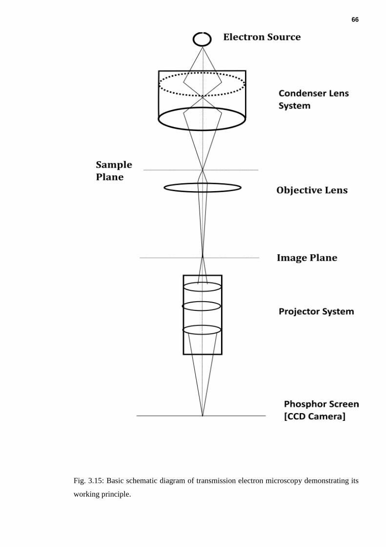
66
Fig. 3.15: Basic schematic diagram of transmission electron microscopy demonstrating its
working principle.

67
As shown in the above figure, the electron source of the microscope generates a high energy
electron beam. A two stage condenser lens system is used to focus the electron beam on the
sample. There is an aperture immediately after the condenser lens system. The ‘brightness’
of the image is controlled by the condenser system. The objective lens forms an inverted
image (with a small degree of magnification) of the sample by focussing the transmitted
electron beam in a virtual image plane. The focal length of the lens can be changed by
adjusting the current passing through the electromagnetic coil that makes up the objective
lens. An objective aperture may be inserted to select electrons which will form the image
(selecting specific diffraction spots for dark field imaging). The projection system forms a
magnified image in the recording device. The magnification of the microscope can vary
from a few hundred to several hundred thousand depending on the setting of the strength of
the projector lenses.
By adjusting the projection lens system, we can also image the diffraction pattern formed
due to the interaction between the electron beam and the sample at the back focal plane of
the objective lens. The diffraction pattern can reveal much useful information about the
structural properties of the sample under investigation.
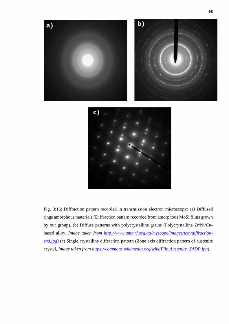
68
Fig. 3:16: Diffraction pattern recorded in transmission electron microscopy: (a) Diffused
rings amorphous materials (Diffraction pattern recorded from amorphous MoSi films grown
by our group). (b) Diffuse patterns with polycrystalline grains (Polycrystalline Zr/Ni/Cu-
based alloy, Image taken from http://www.ammrf.org.au/myscope/images/tem/diffraction-
sad.jpg) (c) Single crystalline diffraction pattern (Zone axis diffraction pattern of austenite
crystal, Image taken from https://commons.wikimedia.org/wiki/File:Austenite_ZADP.jpg).
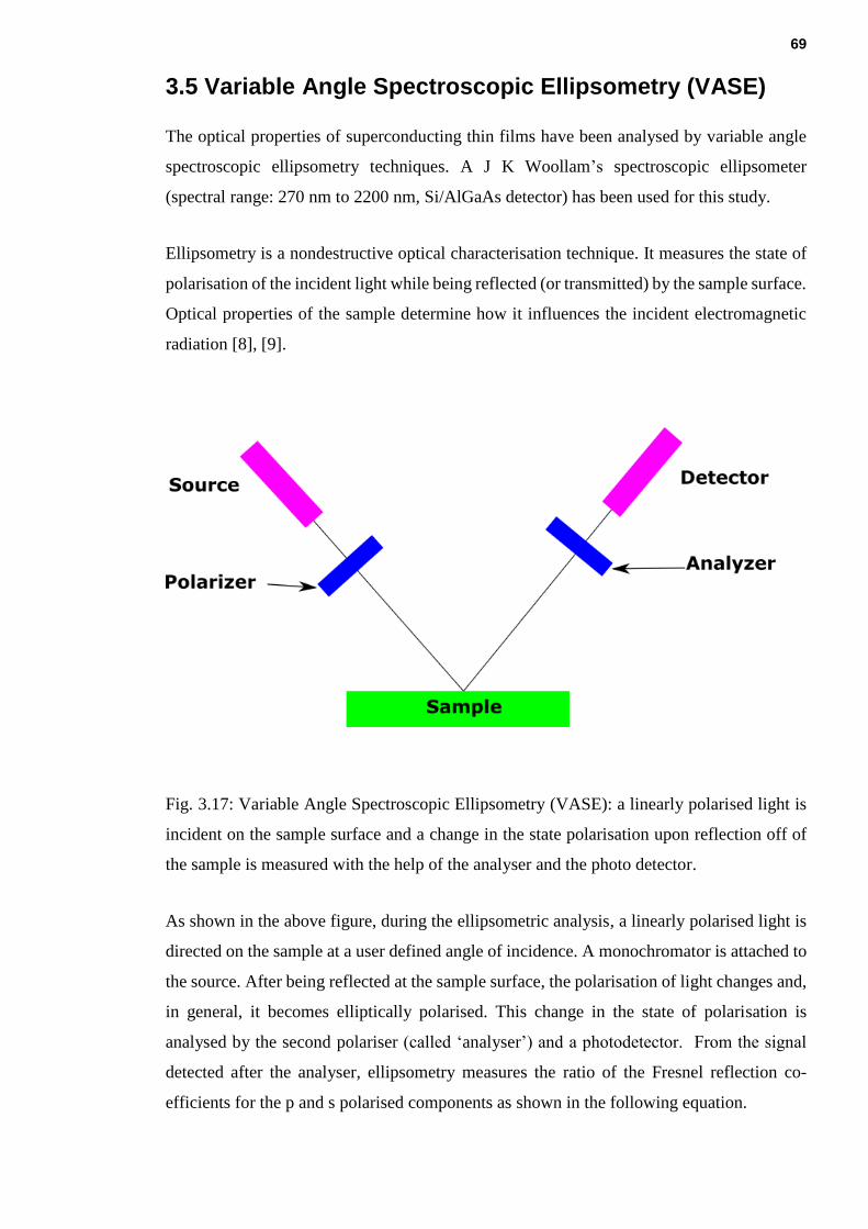
69
3.5 Variable Angle Spectroscopic Ellipsometry (VASE)
The optical properties of superconducting thin films have been analysed by variable angle
spectroscopic ellipsometry techniques. A J K Woollam’s spectroscopic ellipsometer
(spectral range: 270 nm to 2200 nm, Si/AlGaAs detector) has been used for this study.
Ellipsometry is a nondestructive optical characterisation technique. It measures the state of
polarisation of the incident light while being reflected (or transmitted) by the sample surface.
Optical properties of the sample determine how it influences the incident electromagnetic
radiation [8], [9].
Fig. 3.17: Variable Angle Spectroscopic Ellipsometry (VASE): a linearly polarised light is
incident on the sample surface and a change in the state polarisation upon reflection off of
the sample is measured with the help of the analyser and the photo detector.
As shown in the above figure, during the ellipsometric analysis, a linearly polarised light is
directed on the sample at a user defined angle of incidence. A monochromator is attached to
the source. After being reflected at the sample surface, the polarisation of light changes and,
in general, it becomes elliptically polarised. This change in the state of polarisation is
analysed by the second polariser (called ‘analyser’) and a photodetector. From the signal
detected after the analyser, ellipsometry measures the ratio of the Fresnel reflection co-
efficients for the p and s polarised components as shown in the following equation.

70
𝜌 =𝑟𝑝
𝑟𝑠= tan (𝜓)exp (𝑖𝛥𝑣) (3.1)
The above equation is the fundamental equation of ellipsometry. Here, rp and rs denote the
Fresnel reflection co-efficient for the p and s polarised components. tan (𝜓) and 𝛥𝑣 are the
amplitude change and phase shift of the incident light upon reflection. (p polarised light
denotes light polarised parallel to the plane of incidence and s polarised light denotes light
polarised perpendicular to the plane of incidence.) Measured data is usually expressed as a
function of 𝜓 and 𝛥𝑣 as shown in equation 3.1. The angle of incidence is usually kept close
to the Brewster angle so that the measured ratio can be maximised.
To retrieve important information (e.g. thickness, refractive index, etc.) from the
ellipsometric measurement, we need to construct a model which is suitable for the sample
which is being measured. After constructing the model, we take the help of different fitting
algorithms of the analysis software provided with the instrument (WVASE32 version 3.840)
to fit the theoretical model with the 𝜓 and Δ𝑣 measurement data. It is to be noted that
ellipsometric measurement strongly depends on the modelling as we cannot extract useful
optical or physical parameters only from the measured data. For the superconducting thin
films we have used a combination of Drude and Lorentz oscillator models to describe their
optical properties.
3.6 Nanowire patterning of superconducting thin films
The transport properties, including the temperature dependence of the critical current density
of amorphous superconducting thin films, have been measured from the low temperature
measurements of nanowires patterned on the films. Electron beam lithography (EBL) and
reactive ion etching (RIE) have been used for this purpose. Here, we have given a brief
overview of the fabrication procedure which has been followed to fabricate the nanowires.
At the beginning, amorphous MoSi film (~ 10 nm thick) is grown on the top of the silicon
substrate. Then, ZEP 520 A (a positive tone electron beam resist) is spun at 4000 rpm for 60
seconds and baked for four minutes (leading to a thickness of 110 nm). EBL is used to define
the patterns for alignment markers and contact pads. A Vistec VB6 UHR EHF EBL tool at
100 keV has been used for all the EBL patterning. Then the chip is developed in Oxylene (at
23°C temperature), leaving only the unexposed resist. 15nm Ti and then 75 nm Au is
deposited on the device by electron beam evaporation. The Ti layer works as an adhesive
layer between the Au layer and the Si substrate. The resist along with the unwanted Au is

71
removed by putting the chip in a 1165-Stripper solvent overnight. After that, the nanowires
are patterned over the thin film. A second round of the EBL process is performed in a similar
way to steps 2–4 to create the pattern. Reactive Ion Etching (RIE) removes the thin film
unshielded by the resist (CF4 gas). The remaining resist is stripped using Shipley 1165
microposit remover.
Fig. 3.18: Nanowire fabrication: 1: Deposition of superconducting thin film on Silicon
substrate. 2. Spinning of ZEP 520 A (a positive tone electron beam resist) at 4000 rotations
per minute (rpm) for 60 seconds and baked for four minutes. 3. Exposure to the electron
beam to define patterns for contact pads and alignment markers. 4. Development in Oxylene
(at 23°C temperature) for 60 seconds. 5. Deposition of 15 nm Ti and then 75 nm Au using
electron beam evaporation. 6. Removal of resist along with the unwanted Au by putting the
chip in 1165-Stripper solvent overnight. 7-9. Nanowire patterns are defined using a second
round of EBL. 10. Reactive Ion Etching (RIE) removes the thin film unshielded by the resist
(CF4 gas). 11. The remaining resist is stripped using Shipley 1165 microposit remover.
72
References
[1] J. George, Preparation of thin films. M. Dekker, 1992.
[2] M. Leskela and M. Ritalä, “Atomic layer deposition ( ALD ) : from precursors to
thin film structures,” Thin Solid Films, vol. 409, pp. 138–146, 2002.
[3] E. Alfonso, J. Olaya, and G. Cubillos, “Thin Film Growth Through Sputtering
Technique and Its Applications,” in Crystallization - Science and Technology,
InTech, 2012, pp. 397-432.
[4] R. W. Johnson, A. Hultqvist, and S. F. Bent, “A brief review of atomic layer
deposition: from fundamentals to applications,” Mater. Today, vol. 17, no. 5, pp.
236–246, Jun. 2014.
[5] W. E. Gifford and R. C. Longsworth, “Surface Heat Pumping,” in Advances in
Cryogenic Engineering, Boston, MA: Springer US, 1966, pp. 171–179.
[6] L. A. Giannuzzi and F. A. Stevie, “A review of focused ion beam milling techniques
for TEM specimen preparation,” Micron, vol. 30, no. 3, pp. 197–204, 1999.
[7] D. B. Williams and C. B. Carter, Transmission Electron Microscopy. Boston, MA:
Springer US, 2009.
[8] J. A. Woollam and P. G. Snyder, “Fundamentals and applications of variable angle
spectroscopic ellipsometry,” Mater. Sci. Eng. B, vol. 5, no. 2, pp. 279–283, Jan.
1990.
[9] J. A. Woollam, P. G. Snyder, and M. C. Rost, “Variable angle spectroscopic
ellipsometry: A non-destructive characterization technique for ultrathin and
multilayer materials,” Thin Solid Films, vol. 166, pp. 317–323, Dec. 1988.
73
Chapter 4
Optimisation of Niobium (Nb), Niobium Nitride
(NbN) and Niobium Titanium Nitride (NbTiN) Thin
Film Growth
Since the fabrication of superconducting nanowire single photon detectors (SNSPDs) begins
with superconducting thin film deposition, the quality of the films plays a vital role
determining device performance. Nb based refractory metal nitrides (NbN & NbTiN) are the
most widely used traditional thin film material for SNSPD applications. In this chapter, the
growth and optimisation of NbTiN thin films have been reported (Section 4.2). Structural
and optical characterisation of NbTiN films have also been discussed (Section 4.4 & 4.5).
The acceptance test of the sputter deposition system (Section 4.1) and the process developed
for NbN has been reported (Section 4.3). The chapter concludes with a short discussion on
the SNSPD device fabrication based on the films deposited following the optimised process
described in this chapter (Section 4.6).
4.1 Acceptance test of sputter deposition system
Immediately after the installation of the sputter deposition system, we started with the
optimisation of thick superconducting niobium film. A 300 nm thick niobium film was
deposited in our sputtering system (at 0.2 Pa chamber pressure, 0.9 A discharge current) and
transition temperature was measured in the thin film testing set-up. The following figure
presents resistance versus temperature data (Fig. 4.1). The film has a transition temperature
of 9.1 K, which is close to the transition temperature of bulk niobium. This was a part of the
acceptance test for the sputter deposition system.4
4 In the literature, there are several definitions of Tc. We define it as the temperature at which
resistance of the film disappears or falls to zero in the R vs. T curve.

74
Fig. 4.1: Resistance versus Temperature curve of 300 nm thick niobium film deposited on a
silicon substrate (zoomed in view) demonstrating a Tc of 9.1 K.
It is observed from the R vs T curve (Fig. 4.2) that resistance of the niobium film steadily
decreases with temperature during the cool-down process. Hence, the film is purely metallic
in nature. The residual resistivity ratio (RRR) of the film is 4.4.

75
Fig. 4.2: Resistance versus Temperature curve of 300 nm thick niobium film deposited on a
silicon substrate.
4.2 Niobium Titanium Nitride Growth and Characterisation
As discussed in the Section 2.4 of Chapter 2, the fabrication process of a superconducting
nanowire single photon detector (SNSPD) initiates with superconducting thin films growth.
For the operation of an SNSPD, ultrathin superconducting films (with a thickness of < 10
nm) are required which can be cooled down below their transition temperatures using a 2
stage cryo-coolers (to avoid expensive and hazardous cryogenic liquids). Gol'tsman et al.
used NbN film in their initial SNSPD devices [1]. Until now, NbN & NbTiN are the most
extensively used base materials for SNSPD fabrication (due to their higher bulk critical
temperature and shorter coherence length) [2]. Hence, we have started our thin film
optimization with NbTiN and NbN.
4.2.1 Choice of substrate and deposition conditions
At first, NbTiN film growth has been optimised in terms of desirable thickness, uniformity
and superconducting properties. As was stated earlier in Section 2.4 of Chapter 2, since the
76
lattice parameters of MgO or sapphire are very close to that of NbTiN, they have been widely
used as substrates for NbN or NbTiN based SNSPDs. However, this limited choice of
substrates restricts the potential application of SNSPDs. That is why we chose silicon as our
substrate for optimisation. Silicon is an attractive substrate material for various applications
at telecommunication wavelength. It also has an advanced and mature fabrication
technology. Single side polished silicon wafers with <001> crystalline direction have been
diced into 15 mm x 15 mm sized substrates and have been used for NbN & NbTiN growth
optimisation.
Before deposition, the substrates have been cleaned in an ultrasonic bath with RO water,
acetone and IPA for 5 minutes. Then, the substrates are inserted in the loadlock of the sputter
deposition tool. Prior to the film deposition, substrates were etched into the loadlock with
argon plasma for 2 minutes. After that, they are transferred to the main chamber with the
automated transfer arm. NbTiN films are grown by the co-sputtering of confocal Nb and Ti
targets in an argon environment and introducing a small amount of nitrogen in the chamber
as the reactive gas. The distance between the substrate and the target is kept at 100 mm. The
substrate holder was rotated at a speed of 60 rpm during deposition for better uniformity of
the film growth. While executing the deposition process, the cryo gate valve of the chamber
is closed. The turbo pump is throttled with a butterfly valve to maintain the desired pressure
in the chamber.
4.2.2 Choice between Current and Voltage Controlled Deposition
Thin film growth process in DC magnetron sputtering can be controlled by the constant
current mode, constant voltage mode or constant power mode. Yagoubov et al. [3] have
discussed a potential approach to monitoring the NbN sputtering process and avoiding the
hysteresis formation. According to their study, if NbN (or NbTiN) films are sputtered at a
constant voltage or power mode, there is a possibility of the formation of a hysteresis loop
in the I-V curve due to the unstable state of the discharge plasma. Fig. 4.3 depicts such a
curve (I-V curve during reactive sputtering of NbN in the constant voltage mode).
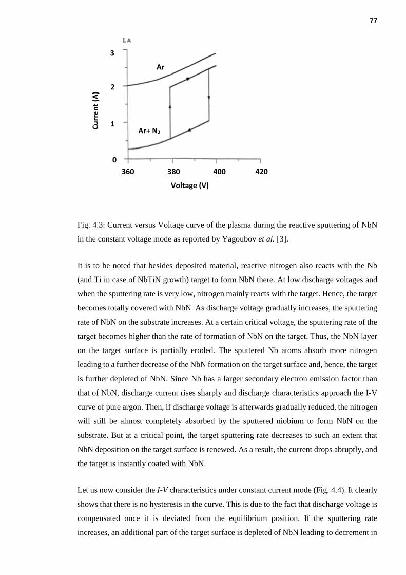
77
Fig. 4.3: Current versus Voltage curve of the plasma during the reactive sputtering of NbN
in the constant voltage mode as reported by Yagoubov et al. [3].
It is to be noted that besides deposited material, reactive nitrogen also reacts with the Nb
(and Ti in case of NbTiN growth) target to form NbN there. At low discharge voltages and
when the sputtering rate is very low, nitrogen mainly reacts with the target. Hence, the target
becomes totally covered with NbN. As discharge voltage gradually increases, the sputtering
rate of NbN on the substrate increases. At a certain critical voltage, the sputtering rate of the
target becomes higher than the rate of formation of NbN on the target. Thus, the NbN layer
on the target surface is partially eroded. The sputtered Nb atoms absorb more nitrogen
leading to a further decrease of the NbN formation on the target surface and, hence, the target
is further depleted of NbN. Since Nb has a larger secondary electron emission factor than
that of NbN, discharge current rises sharply and discharge characteristics approach the I-V
curve of pure argon. Then, if discharge voltage is afterwards gradually reduced, the nitrogen
will still be almost completely absorbed by the sputtered niobium to form NbN on the
substrate. But at a critical point, the target sputtering rate decreases to such an extent that
NbN deposition on the target surface is renewed. As a result, the current drops abruptly, and
the target is instantly coated with NbN.
Let us now consider the I-V characteristics under constant current mode (Fig. 4.4). It clearly
shows that there is no hysteresis in the curve. This is due to the fact that discharge voltage is
compensated once it is deviated from the equilibrium position. If the sputtering rate
increases, an additional part of the target surface is depleted of NbN leading to decrement in
Ar+ N2
Ar
360 380 400 420
Voltage (V)
0
1
2
3
Cu
rren
t (A
)

78
nitrogen partial pressure. This will reduce discharge voltage (since the presence of nitrogen
enhances impedance of argon plasma in the discharge). Hence, the sputtering rate returns to
its initial value. The converse will occur if the sputtering rate decreases. Hence, it is possible
to obtain a one-to-one correspondence between discharge voltage and nitrogen flow at
constant current mode operation. Therefore, the change in discharge voltage due to the
introduction of nitrogen into the chamber may be used as a suitable parameter to control
nitrogen partial pressure in the system.
Fig. 4.4: Current-Voltage curve when NbN is deposited in constant current stabilisation
condition [3].
Later on, many other groups (for instance Marsili et al., Matsunaga et al., etc.) have utilised
this concept to optimise NbN or NbTiN thin film deposition in reactive sputtering [4], [5].
In this study, we have also used a constant current controlled approach.
4.2.3 Characterisation of Plasma
At the beginning of the film growth, we have explored the target voltage vs nitrogen flow
curve of niobium plasma in order to set a starting value of nitrogen flow for optimisation.
Ar+ N2
Ar
360 380 400 420
ΔV
Voltage (V)
0
1
2
3
Cu
rren
t (A
)
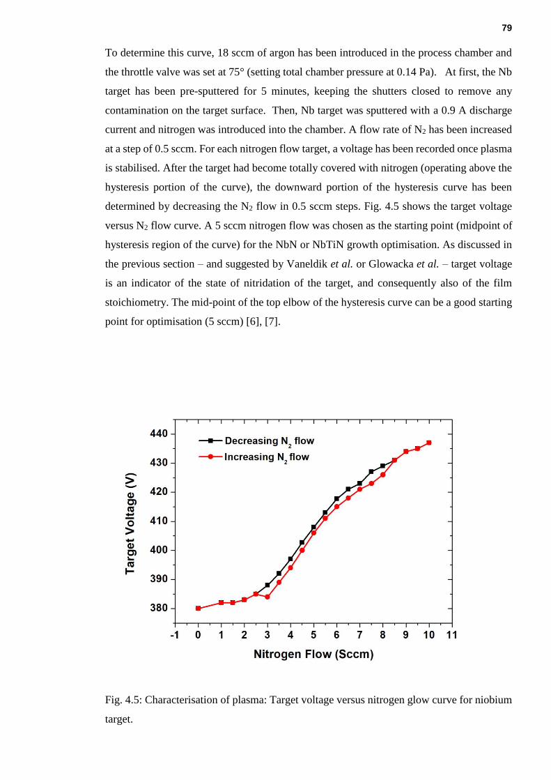
79
To determine this curve, 18 sccm of argon has been introduced in the process chamber and
the throttle valve was set at 75° (setting total chamber pressure at 0.14 Pa). At first, the Nb
target has been pre-sputtered for 5 minutes, keeping the shutters closed to remove any
contamination on the target surface. Then, Nb target was sputtered with a 0.9 A discharge
current and nitrogen was introduced into the chamber. A flow rate of N2 has been increased
at a step of 0.5 sccm. For each nitrogen flow target, a voltage has been recorded once plasma
is stabilised. After the target had become totally covered with nitrogen (operating above the
hysteresis portion of the curve), the downward portion of the hysteresis curve has been
determined by decreasing the N2 flow in 0.5 sccm steps. Fig. 4.5 shows the target voltage
versus N2 flow curve. A 5 sccm nitrogen flow was chosen as the starting point (midpoint of
hysteresis region of the curve) for the NbN or NbTiN growth optimisation. As discussed in
the previous section – and suggested by Vaneldik et al. or Glowacka et al. – target voltage
is an indicator of the state of nitridation of the target, and consequently also of the film
stoichiometry. The mid-point of the top elbow of the hysteresis curve can be a good starting
point for optimisation (5 sccm) [6], [7].
Fig. 4.5: Characterisation of plasma: Target voltage versus nitrogen glow curve for niobium
target.
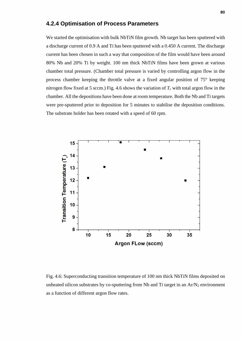
80
4.2.4 Optimisation of Process Parameters
We started the optimisation with bulk NbTiN film growth. Nb target has been sputtered with
a discharge current of 0.9 A and Ti has been sputtered with a 0.450 A current. The discharge
current has been chosen in such a way that composition of the film would have been around
80% Nb and 20% Ti by weight. 100 nm thick NbTiN films have been grown at various
chamber total pressure. (Chamber total pressure is varied by controlling argon flow in the
process chamber keeping the throttle valve at a fixed angular position of 75° keeping
nitrogen flow fixed at 5 sccm.) Fig. 4.6 shows the variation of Tc with total argon flow in the
chamber. All the depositions have been done at room temperature. Both the Nb and Ti targets
were pre-sputtered prior to deposition for 5 minutes to stabilise the deposition conditions.
The substrate holder has been rotated with a speed of 60 rpm.
Fig. 4.6: Superconducting transition temperature of 100 nm thick NbTiN films deposited on
unheated silicon substrates by co-sputtering from Nb and Ti target in an Ar/N2 environment
as a function of different argon flow rates.

81
From the Fig. 4.6 it can be clearly seen that a maximum Tc of 15.1 K is achieved if NbTiN
is grown with 18 sccm Ar and 5 sccm N2. (This corresponds to a total chamber pressure of
0.14 Pa.) A deposition time of 6 minutes has been used to deposit 100 nm thick films.
Fig. 4.7: Normalised Resistance versus Temperature of 100 nm thick NbTiN film deposited
at various nitrogen flows keeping the total chamber pressure constant at 0.14 Pa.
After that, the total chamber pressure has been fixed at 0.14 Pa and 100 nm thick NbTiN
film was deposited at different nitrogen flow rates when other deposition parameters were
kept unchanged. As it can be seen from the Fig. 4.7, a maximum Tc of 15.1 K can be achieved
from a film grown with 5 sccm N2 flow. We have also checked the influence of other
deposition parameters (e.g. Nb:Ti ratio or substrate holder rotation) on superconducting
property of the film. The above mentioned process parameters give an optimum Tc for 100
nm thick NbTiN film deposited at room temperature.

82
4.2.5 Process Optimisation for ultrathin NbTiN Films (thickness <10 nm)
As mentioned in Chapter 2, decreasing film thickness results in the degradation of
superconducting and electrical properties of thin films. To explore this thickness
dependence, NbTiN films ranging from 100 to 5.5 nm in thickness were deposited on silicon
substrates under the same optimised deposition conditions. The thickness of the films has
been reduced by decreasing the deposition time.
Table 4.1: Optimised Recipe for NbTiN Deposition
Nb 0.9 A (356 W, 398 V)
Ti 0.450 A (179 W, 399 V)
Target Substrate Distance
100 mm
Substrate Holder Rotation
60 Rotation per minute
Ar Flow 18 sccm
N2Flow 5 sccm
Throttle Position
75°
Chamber Pressure
0.14 Pa
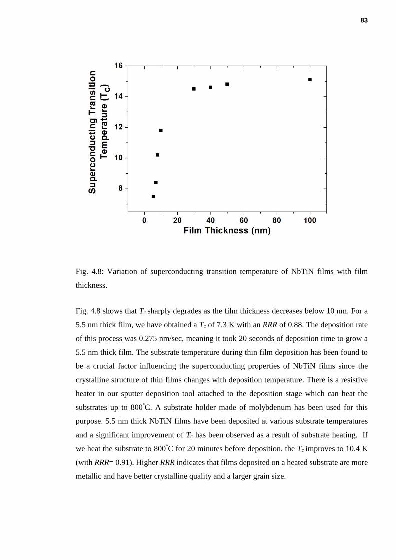
83
Fig. 4.8: Variation of superconducting transition temperature of NbTiN films with film
thickness.
Fig. 4.8 shows that Tc sharply degrades as the film thickness decreases below 10 nm. For a
5.5 nm thick film, we have obtained a Tc of 7.3 K with an RRR of 0.88. The deposition rate
of this process was 0.275 nm/sec, meaning it took 20 seconds of deposition time to grow a
5.5 nm thick film. The substrate temperature during thin film deposition has been found to
be a crucial factor influencing the superconducting properties of NbTiN films since the
crystalline structure of thin films changes with deposition temperature. There is a resistive
heater in our sputter deposition tool attached to the deposition stage which can heat the
substrates up to 800°C. A substrate holder made of molybdenum has been used for this
purpose. 5.5 nm thick NbTiN films have been deposited at various substrate temperatures
and a significant improvement of Tc has been observed as a result of substrate heating. If
we heat the substrate to 800°C for 20 minutes before deposition, the Tc improves to 10.4 K
(with RRR= 0.91). Higher RRR indicates that films deposited on a heated substrate are more
metallic and have better crystalline quality and a larger grain size.
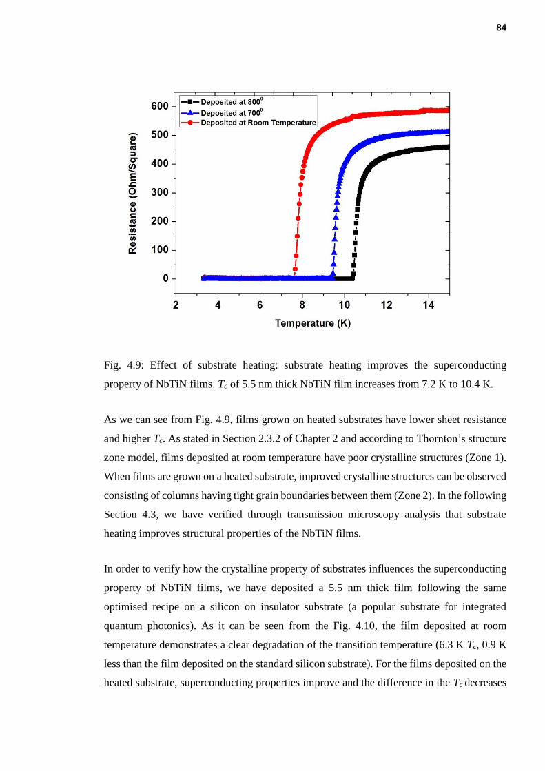
84
Fig. 4.9: Effect of substrate heating: substrate heating improves the superconducting
property of NbTiN films. Tc of 5.5 nm thick NbTiN film increases from 7.2 K to 10.4 K.
As we can see from Fig. 4.9, films grown on heated substrates have lower sheet resistance
and higher Tc. As stated in Section 2.3.2 of Chapter 2 and according to Thornton’s structure
zone model, films deposited at room temperature have poor crystalline structures (Zone 1).
When films are grown on a heated substrate, improved crystalline structures can be observed
consisting of columns having tight grain boundaries between them (Zone 2). In the following
Section 4.3, we have verified through transmission microscopy analysis that substrate
heating improves structural properties of the NbTiN films.
In order to verify how the crystalline property of substrates influences the superconducting
property of NbTiN films, we have deposited a 5.5 nm thick film following the same
optimised recipe on a silicon on insulator substrate (a popular substrate for integrated
quantum photonics). As it can be seen from the Fig. 4.10, the film deposited at room
temperature demonstrates a clear degradation of the transition temperature (6.3 K Tc, 0.9 K
less than the film deposited on the standard silicon substrate). For the films deposited on the
heated substrate, superconducting properties improve and the difference in the Tc decreases

85
to 0.2 K. Hence, it can be inferred that due to its polycrystalline nature, superconducting
properties of NbTiN can be highly influenced by substrates.
Fig. 4.10: Superconducting property of 5.5 nm thick NbTiN film deposited on silicon and
silicon on insulator (SoI) substrates with and without heating.
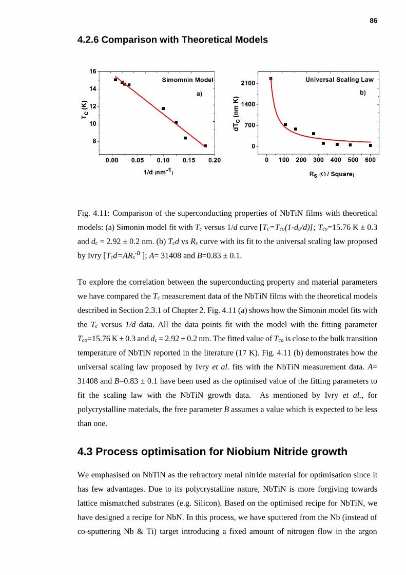
86
4.2.6 Comparison with Theoretical Models
Fig. 4.11: Comparison of the superconducting properties of NbTiN films with theoretical
models: (a) Simonin model fit with Tc versus 1/d curve [Tc=Tco(1-dc/d)]; Tco=15.76 K ± 0.3
and dc = 2.92 ± 0.2 nm. (b) Tcd vs Rs curve with its fit to the universal scaling law proposed
by Ivry [Tcd=ARs-B ]; A= 31408 and B=0.83 ± 0.1.
To explore the correlation between the superconducting property and material parameters
we have compared the Tc measurement data of the NbTiN films with the theoretical models
described in Section 2.3.1 of Chapter 2. Fig. 4.11 (a) shows how the Simonin model fits with
the Tc versus 1/d data. All the data points fit with the model with the fitting parameter
Tco=15.76 K ± 0.3 and dc = 2.92 ± 0.2 nm. The fitted value of Tco is close to the bulk transition
temperature of NbTiN reported in the literature (17 K). Fig. 4.11 (b) demonstrates how the
universal scaling law proposed by Ivry et al. fits with the NbTiN measurement data. A=
31408 and B=0.83 ± 0.1 have been used as the optimised value of the fitting parameters to
fit the scaling law with the NbTiN growth data. As mentioned by Ivry et al., for
polycrystalline materials, the free parameter B assumes a value which is expected to be less
than one.
4.3 Process optimisation for Niobium Nitride growth
We emphasised on NbTiN as the refractory metal nitride material for optimisation since it
has few advantages. Due to its polycrystalline nature, NbTiN is more forgiving towards
lattice mismatched substrates (e.g. Silicon). Based on the optimised recipe for NbTiN, we
have designed a recipe for NbN. In this process, we have sputtered from the Nb (instead of
co-sputtering Nb & Ti) target introducing a fixed amount of nitrogen flow in the argon
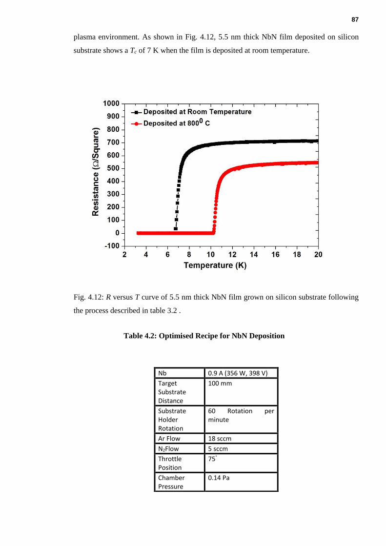
87
plasma environment. As shown in Fig. 4.12, 5.5 nm thick NbN film deposited on silicon
substrate shows a Tc of 7 K when the film is deposited at room temperature.
Fig. 4.12: R versus T curve of 5.5 nm thick NbN film grown on silicon substrate following
the process described in table 3.2 .
Table 4.2: Optimised Recipe for NbN Deposition
Nb 0.9 A (356 W, 398 V)
Target Substrate Distance
100 mm
Substrate Holder Rotation
60 Rotation per minute
Ar Flow 18 sccm
N2Flow 5 sccm
Throttle Position
75°
Chamber Pressure
0.14 Pa

88
4.4 High resolution scanning transmission electron microscopy analysis
We have analysed a specific selection of NbTiN films in high resolution TEM. Samples have
been prepared for TEM analysis following the process described in Section 3.4 of Chapter
3. A JEOL ARM200cF microscope has been used for this analysis. Fig. 4.13 shows the TEM
images (400 KX) of a 6.5 nm thick NbTiN film deposited at room temperature and at 800°C.
The ordered structure of the crystalline silicon substrate is seen on the left hand side of the cross
section image. Between the film and the substrate, there is a native oxide layer. The cross section
also shows epitaxial growth of films with a smooth and sharp interface. We have measured the
thickness of the layers at several locations for both the films. NbTiN and native oxide layers
have a thickness of 6.7 nm (± 0.2 nm) and 2.5 nm (± 0.3 nm) respectively. Line profile analysis
of digital micrograph software has been used to extract thickness of all the layers. As can be seen
from the line profiles for the film deposited at room temperature and the film deposited on the
heated substrate, the substrate heating does not affect film thickness or deposition rate.
Fig .4.13 TEM cross-section image of a 6.5 nm thick NbTiN film deposited at room
temperature.
Silicon Substrate
NbTiN Film
Native Oxide Layer
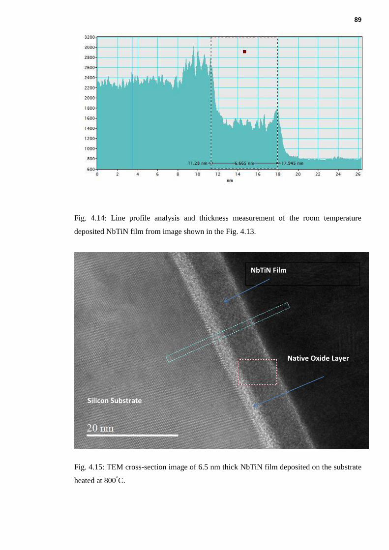
89
Fig. 4.14: Line profile analysis and thickness measurement of the room temperature
deposited NbTiN film from image shown in the Fig. 4.13.
Fig. 4.15: TEM cross-section image of 6.5 nm thick NbTiN film deposited on the substrate
heated at 800°C.
Silicon Substrate
NbTiN Film
Native Oxide Layer
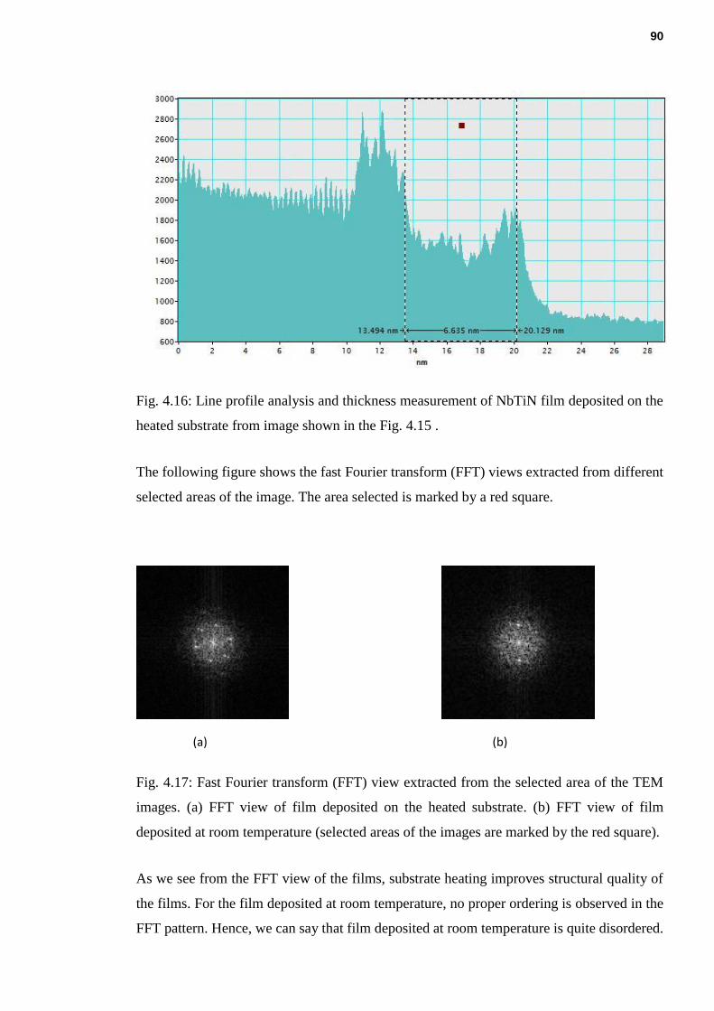
90
Fig. 4.16: Line profile analysis and thickness measurement of NbTiN film deposited on the
heated substrate from image shown in the Fig. 4.15 .
The following figure shows the fast Fourier transform (FFT) views extracted from different
selected areas of the image. The area selected is marked by a red square.
(a) (b)
Fig. 4.17: Fast Fourier transform (FFT) view extracted from the selected area of the TEM
images. (a) FFT view of film deposited on the heated substrate. (b) FFT view of film
deposited at room temperature (selected areas of the images are marked by the red square).
As we see from the FFT view of the films, substrate heating improves structural quality of
the films. For the film deposited at room temperature, no proper ordering is observed in the
FFT pattern. Hence, we can say that film deposited at room temperature is quite disordered.
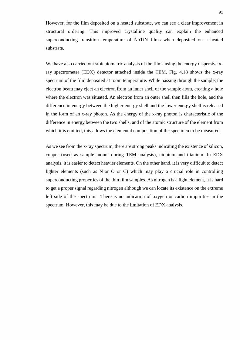
91
However, for the film deposited on a heated substrate, we can see a clear improvement in
structural ordering. This improved crystalline quality can explain the enhanced
superconducting transition temperature of NbTiN films when deposited on a heated
substrate.
We have also carried out stoichiometric analysis of the films using the energy dispersive x-
ray spectrometer (EDX) detector attached inside the TEM. Fig. 4.18 shows the x-ray
spectrum of the film deposited at room temperature. While passing through the sample, the
electron beam may eject an electron from an inner shell of the sample atom, creating a hole
where the electron was situated. An electron from an outer shell then fills the hole, and the
difference in energy between the higher energy shell and the lower energy shell is released
in the form of an x-ray photon. As the energy of the x-ray photon is characteristic of the
difference in energy between the two shells, and of the atomic structure of the element from
which it is emitted, this allows the elemental composition of the specimen to be measured.
As we see from the x-ray spectrum, there are strong peaks indicating the existence of silicon,
copper (used as sample mount during TEM analysis), niobium and titanium. In EDX
analysis, it is easier to detect heavier elements. On the other hand, it is very difficult to detect
lighter elements (such as N or O or C) which may play a crucial role in controlling
superconducting properties of the thin film samples. As nitrogen is a light element, it is hard
to get a proper signal regarding nitrogen although we can locate its existence on the extreme
left side of the spectrum. There is no indication of oxygen or carbon impurities in the
spectrum. However, this may be due to the limitation of EDX analysis.

92
Fig. 4.18: Energy dispersive x-ray (EDX) spectrum recorded from the 6.5 nm thick NbTiN
film during HRTEM analysis; the peaks of the spectrum indicate the existence of Nb, Ti, Pt
(deposited as capping during the FIB cross-section) and Si (Substrate).
4.5 Measurement of optical constants for NbN & NbTiN
Accurate measurement of optical constants is crucial to the simulation of optical absorption
in SNSPDs and is a key to integrating these devices with complex optical structures (such
as cavities, nanoantennas and waveguides). The complex refractive index of NbN & NbTiN
films (deposited following the optimised recipe) has been evaluated at room temperature
using a J.A. Woollam & Co. VASE (variable angle spectroscopic ellipsometry) instrument.
We used plasma-enhanced chemical vapour deposition (PECVD) to deposit a 390 nm thick
layer of SiO2 on several silicon substrates. 5.5 nm thick NbN & NbTiN films have been
grown on the top of that at room temperature.
Spectral range of the VASE measurement is from a 270 nm to 2200 nm wavelength (with a
wavelength resolution of 10 nm). Since both the films are optically absorbing all over the
measurement range, it could be difficult to find a unique solution for both the film thickness
and optical parameters due to strong correlations between them. This is why a transparent
layer of SiO2 has been added between the NbN or NbTiN films and substrates. The SiO2
layer underneath the thin films helps to break parameter correlation between optical
constants and film thickness by interference enhancement during the VASE measurement
[8]. The data obtained from ellipsometric measurement has been modelled with a
combination of several Lorentz oscillators. In the following figures, we have shown
refractive index (n) and extinction co-efficient (k) measured from 5.5 nm thick NbN and
NbTiN films. It can be clearly seen that NbTiN film has a higher extinction co-efficient

93
(~10% higher at 1550 nm) than that of NbN film. In a previous study, Anant et al. have
reported optical constants of 12 nm thick NbN film [9]. Their measured values of n & k at
1550 nm were 5.23 and 5.82, which is ~1.5 times higher than our measured value (4.22 and
3.50). This higher value might be due to thicker films they used for VASE measurements.
Fig. 4.19: Complex refractive index measurement of 5.5 nm thick NbTiN and NbN films
using variable angle spectroscopic ellipsometry (VASE) (Both the films have been grown at
room temperature on the silicon substrate).

94
4.6 Device fabrication5
The NbTiN films optimised in this chapter have been used for multi-pixel SNSPD array
fabrication by Dr Alessandro Casaburi. Fig. 4.20 demonstrates a 4 pixel array (60 X 60 um2)
fabricated based on NbTiN film being deposited following the optimised recipe described in
Table 4.1. 7 nm thick films were deposited on Si/SiO2 based DBR substrates at room
temperature for device fabrication. After fabrication, the device shows a Tc of 8 K. Fig. 4.20
(b) shows current versus voltage characteristic curves of all the four pixels measured at 3.6
K. It can be seen that one pixel has a critical current (Ic) of 44 µA while others show Ic
between 50-54 µA. At 1550 nm, the best performing pixel has shown 35% system detection
efficiency at 1 kHz dark count rate.
Fig. 4.20: Superconducting device fabrication based on the films grown following the
optimised process described in this chapter: (a) SEM image of a 4 pixel array (60 X 60 µm2)
fabricated based on 7 nm thick NbTiN film. (b) R(T) curve of the device indicating a Tc of 8
K (c) Current-Voltage curves of all the four pixels measured at 3.6 K. (d) System Detection
Efficiency versus dark counts measured at 1550 nm.
5 SNSPD device fabrication based on NbTiN thin film and its characterisation has been performed by
Dr. Alessandro Casaburi.

95
4.7 Summary
In this chapter, we have reported the growth and optimisation of refractory metal nitrides
with an emphasis on NbTiN. Following the optimised process, a Tc of 7.2 K has been
achieved for a 5.5 nm thick NbTiN film grown on a silicon substrate. When we heat the
substrate up to 800°C, a NbTiN film with the same thickness shows a transition temperature
of 10.4 K. Higher Tc and a lower sheet resistance of the films grown on the heated substrate
indicate that films deposited at higher temperatures have larger grains and better crystalline
structures. Comparison of Tc measurement data with the theoretical models (Ivry and
Simonin) indicates polycrystalline nature of NbTiN films. HRTEM analysis shows that film
thickness or deposition rate is independent of substrate temperature and the structural
property of the thin films improves with substrate heating. Elemental mapping using EDX
analysis confirms that composition of the films consists of Nb, Ti and N2 as expected.
References
[1] G. N. Gol’tsman, O. Okunev, G. Chulkova, A. Lipatov, A. Semenov, K. Smirnov,
B. Voronov, A. Dzardanov, C. Williams, and R. Sobolewski, “Picosecond
superconducting single-photon optical detector,” Appl. Phys. Lett., vol. 79, no. 6, p.
705, Aug. 2001.
[2] C. M. Natarajan, M. G. Tanner, and R. H. Hadfield, “Superconducting nanowire
single-photon detectors: physics and applications,” Supercond. Sci. Technol., vol.
25, no. 6, p. 63001, Jun. 2012.
[3] P. Yagoubov, G. Gol'tsman, B. Voronov, L. Seidman, V. Siomash, and S.
Cherednichenko, “THE BANDWIDTH OF HEB MIXERS EMPLOYING
ULTRATHIN NbN FILMS ON SAPPHIRE SUBSTRATE,” Proc. of the 7th Int.
Symp. on Space Terahertz Tech, pp. 290–302, March 1996.
[4] T. Matsunaga, H. Maezawa, and T. Noguchi, “Characterization of NbTiN thin films
prepared by reactive DC-magnetron sputtering,” IEEE Trans. Appiled Supercond.,
vol. 13, no. 2, pp. 3284–3287, Jun. 2003.
[5] F. Marsili, D. Bitauld, A. Fiore, A. Gaggero, F. Mattioli, R. Leoni, M. Benkahoul,
and F. Lévy, “High efficiency NbN nanowire superconducting single photon
detectors fabricated on MgO substrates from a low temperature process,” Opt.
Express, vol. 16, no. 5, p. 3191, 2008.
[6] J. F. Vaneldik, K. L. Westra, D. Routledge, and M. J. Brett, “Target hysteresis and
film properties of sputtered NbN,” J. Phys. D. Appl. Phys., vol. 22, no. 11, pp.
1788–1790, Nov. 1989.
[7] D. M. Glowacka, D. J. Goldie, S. Withington, H. Muhammad, and G. Yassin,
“Development of a NbN Deposition Process for Superconducting Quantum
Sensors,” Jan. 2014.
[8] J. N. Hilfiker, N. Singh, T. Tiwald, D. Convey, S. M. Smith, J. H. Baker, and H. G.

96
Tompkins, “Survey of methods to characterize thin absorbing films with
Spectroscopic Ellipsometry,” Thin Solid Films, vol. 516, no. 22, pp. 7979–7989,
2008.
[9] V. Anant, “Engineering the optical properties of subwavelength devices and
materials,” P.hD Thesis, Dept. of Electrical Engineering and Computer Science,
Massachusetts Institute of Technology, U.S.A, 2007.

97
Chapter 5
Amorphous Superconducting Thin Films:
Molybdenum Silicide (MoSi) and Molybdenum
Germanium (MoGe)
The crystalline nature of NbN or NbTiN makes the substrate choice for SNSPD very limited,
which sometimes restricts their range of applications. So, amorphous superconducting films
like MoSi or MoGe can be very useful for superconducting detector applications.
Amorphous films do not set strict requirements on substrate choice as there is no issue of
lattice matching. This chapter describes the growth, characterisation and optimisation of
amorphous MoSi and MoGe thin films deposited by co-sputtering in an Ar plasma
environment (Sections 5.1 and 5.2). The correlation between superconducting transition
temperature (Tc), sheet resistance (Rs) and thickness of the films has been compared to
several theoretical models for disordered superconducting films (Section 5.3).
Superconducting and optical properties of amorphous materials must be very sensitive to
short (up to 1 nm) or medium-range order (~1-3 nm) in the atomic structure. Fluctuation
electron microscopy (FEM) studies (an HRTEM analysis technique) showed that the films
assumed an A15 like medium-range order. Electron energy loss spectroscopy (EELS)
indicates that the film stoichiometry was close to Mo83Si17, which is consistent with reports
that many other A15 structures with the nominal formula A3B show a significant non-
stoichiometry with A:B > 3:1 (Section 5.4). Optical properties from ultraviolet (270 nm) to
infrared (2200 nm) wavelengths were measured via variable angle spectroscopic
ellipsometry for 5 nm thick MoSi films and have been compared with the optical properties
of polycrystalline NbN and NbTiN (Section 5.5).
5.1 Molybdenum Silicide deposition
Molybdenum silicide (MoSi) films have been grown on various substrates in the sputter
deposition system (Chapter 3.1). We have co-sputtered from confocal molybdenum (Mo)
and silicon (Si) targets in an argon plasma environment. The distance between the targets
and the substrate is kept at 100 mm. The substrate holder has been rotated at a speed of 60
rotations per minute during the deposition for better uniformity of the film growth. At the
beginning of each deposition cycle, 30 sccm of Argon was introduced into the process
chamber keeping the throttle valve fixed at 80o (setting the total chamber pressure at 0.2 Pa).
Film growth has been initially optimised on a silicon substrate.
98
We have sputtered from the Mo target with a DC power supply at a constant current mode
and silicon target with an impedance matched RF power supply. At first, the discharge
current of the Mo target was fixed at a specific value. Then, the RF power of Si targets was
varied keeping other deposition conditions unchanged to tune the composition of the MoSi
films. Prior to each sample deposition, both the targets were pre-sputtered keeping the
shutters closed for one minute to stabilise the deposition conditions. After that, the same
process had been repeated at several fixed discharge current values for the Mo target,
keeping other chamber parameters unchanged.
Fig. 5.1(a) summarises the variation of Tc of 20 nm thick MoSi films deposited on silicon
substrates as a function of applied power at the Si target for several different Mo discharge
currents. Deposition time was adjusted for each deposition cycle in such a way that the film
thickness remains constant. All the depositions were carried out at room temperature. Fig.
1(b) shows the normalised resistance versus temperature curves for the 20 nm thick MoSi
films deposited with a 0.3 A discharge current applied at a Mo target. Both the figures
indicate that an optimal film composition has been achieved, with a Tc of 7.3 K (and an RRR
of 0.95) for a 0.3 A Mo target discharge current and 125 W Si target RF power. Later on,
the influence of other chamber variables (e.g. substrate holder rotation etc.) on film property
was also checked, which indicates that these deposition parameters are optimum in terms of
film quality. For this optimised growth condition, the film deposition rate was 0.122 nm/sec,
meaning that 2 minutes and 45 seconds of deposition time was used to grow the 20 nm thick
film.
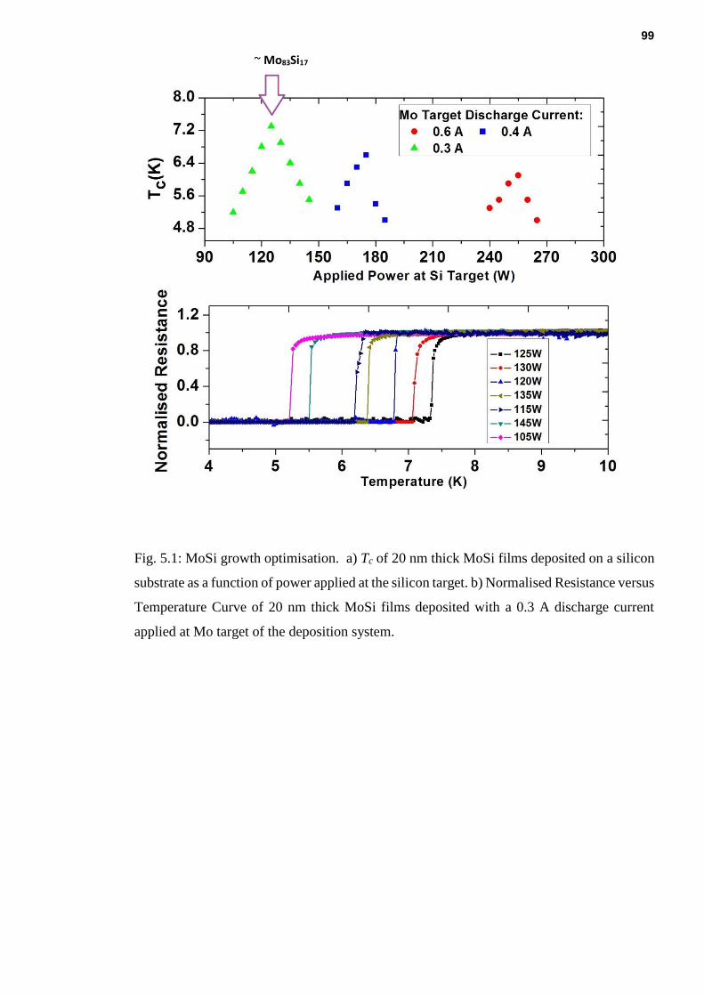
99
Fig. 5.1: MoSi growth optimisation. a) Tc of 20 nm thick MoSi films deposited on a silicon
substrate as a function of power applied at the silicon target. b) Normalised Resistance versus
Temperature Curve of 20 nm thick MoSi films deposited with a 0.3 A discharge current
applied at Mo target of the deposition system.
~ Mo83Si17
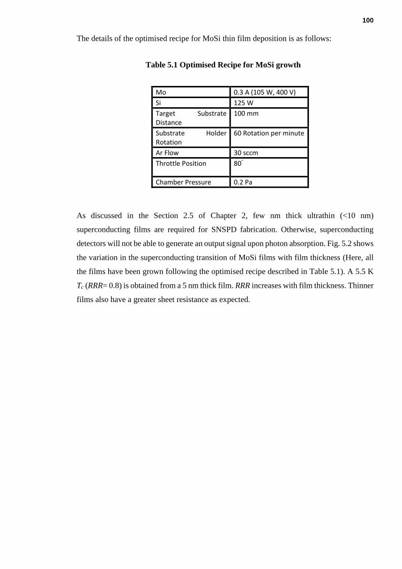
100
The details of the optimised recipe for MoSi thin film deposition is as follows:
Table 5.1 Optimised Recipe for MoSi growth
Mo 0.3 A (105 W, 400 V)
Si 125 W
Target Substrate Distance
100 mm
Substrate Holder Rotation
60 Rotation per minute
Ar Flow 30 sccm
Throttle Position 80°
Chamber Pressure 0.2 Pa
As discussed in the Section 2.5 of Chapter 2, few nm thick ultrathin (<10 nm)
superconducting films are required for SNSPD fabrication. Otherwise, superconducting
detectors will not be able to generate an output signal upon photon absorption. Fig. 5.2 shows
the variation in the superconducting transition of MoSi films with film thickness (Here, all
the films have been grown following the optimised recipe described in Table 5.1). A 5.5 K
Tc (RRR= 0.8) is obtained from a 5 nm thick film. RRR increases with film thickness. Thinner
films also have a greater sheet resistance as expected.

101
Fig. 5.2: R versus T curve of MoSi film with three different thicknesses deposited at room
temperature on a silicon substrate.
5.2 Optimisation of Molybdenum Germanium thin film growth
MoGe is another amorphous TM based superconducting material which can be used for
SNSPD fabrication. Deposition of MoGe superconducting thin films has also been optimised
following a similar process as MoSi. MoGe films have been co-sputtered from confocal Mo
and Ge targets in the argon plasma environment of the UHV deposition system. The distance
between the targets and the substrate is kept at 100 mm. We introduced 30 sccm of argon in
the process chamber keeping the butterfly throttle valve fixed at 80° (total chamber pressure:
0.2 Pa). Molybdenum target have been sputtered with a DC power supply at a constant
current mode and germanium target with an impedance that matched the RF power supply.
The discharge current of Mo target was fixed at a specific value. Then, the RF power of the
Ge target has been varied while other deposition conditions are kept unchanged to tune the
composition of MoGe films.
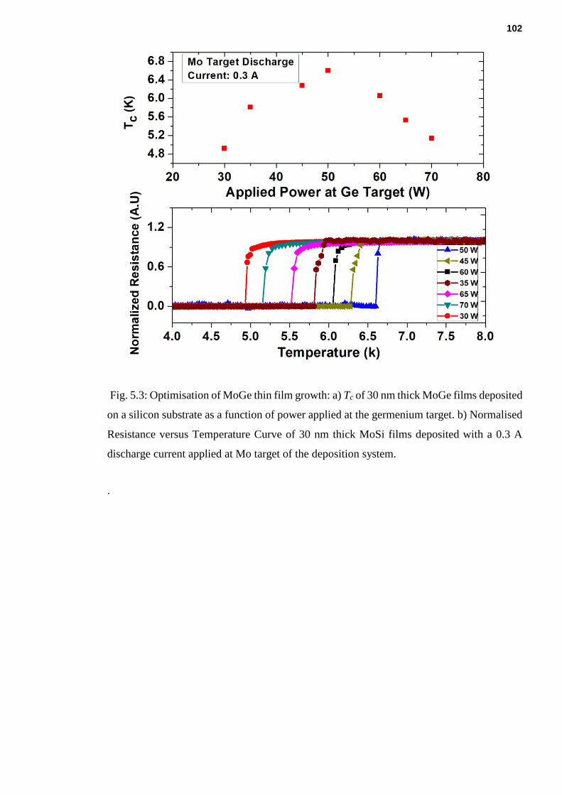
102
Fig. 5.3: Optimisation of MoGe thin film growth: a) Tc of 30 nm thick MoGe films deposited
on a silicon substrate as a function of power applied at the germenium target. b) Normalised
Resistance versus Temperature Curve of 30 nm thick MoSi films deposited with a 0.3 A
discharge current applied at Mo target of the deposition system.
.

103
Fig. 5.4: R versus T curve of MoGe films with three different thicknesses deposited at room
temperature.
The above Fig. 5.3 shows the normalised resistance versus temperature curve of 30 nm thick
MoGe film deposited on a silicon substrate at room temperature for various values of RF
power applied at the Ge target. 2 minutes and 40 seconds (160 seconds) of deposition time
was used when we deposited with a 0.3 A of discharge current at the Mo target. Before
deposition, both Mo and Ge targets were pre-sputtered for one minute with the shutter
closed. Fig. 5.3 shows we get a Tc of 6.6 K (with RRR 0.95) if we deposit a 30 nm thick
MoGe film with a 0.3 A discharge current at a Mo target and 50 W RF power at a Ge target.
Table 5.2 Optimised Recipe for MoGe Growth
Mo 0.3 A (105 W, 400 V)
Ge 50 W
Target Substrate Distance
100 mm
Substrate Holder Rotation
60 Rotations per minute
Ar Flow 30 sccm
Throttle Position 80°
Chamber Pressure 0.2 Pa
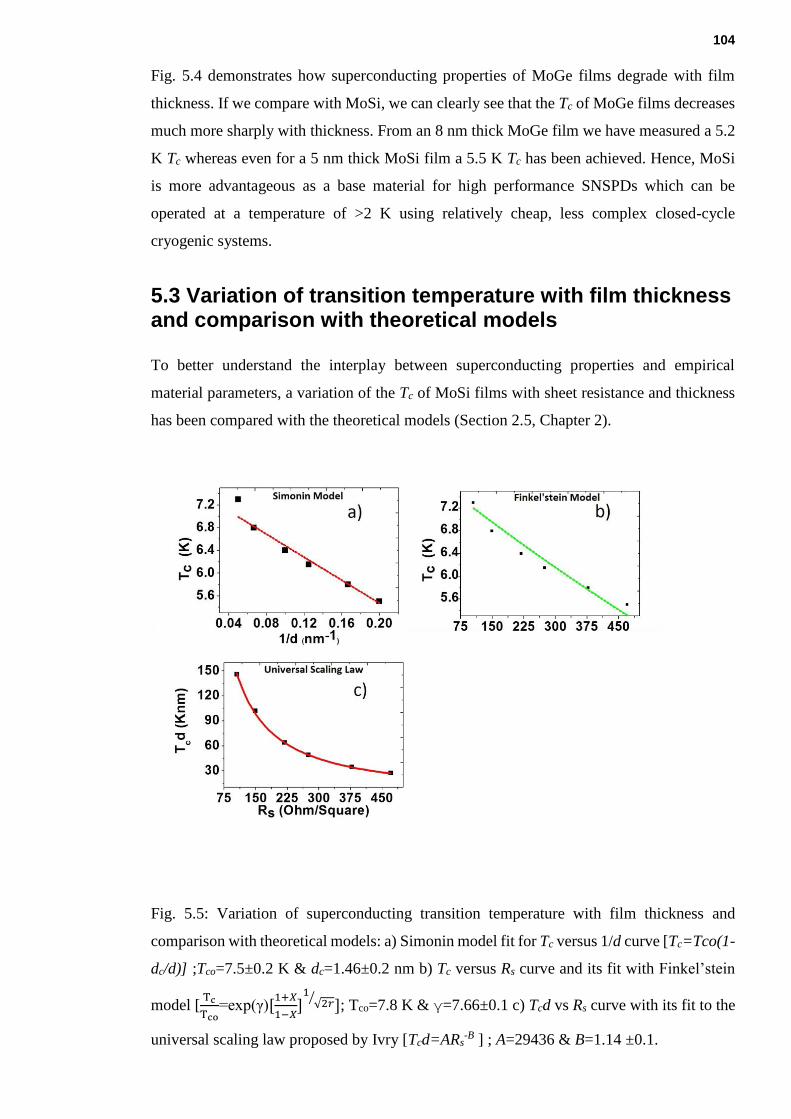
104
Fig. 5.4 demonstrates how superconducting properties of MoGe films degrade with film
thickness. If we compare with MoSi, we can clearly see that the Tc of MoGe films decreases
much more sharply with thickness. From an 8 nm thick MoGe film we have measured a 5.2
K Tc whereas even for a 5 nm thick MoSi film a 5.5 K Tc has been achieved. Hence, MoSi
is more advantageous as a base material for high performance SNSPDs which can be
operated at a temperature of >2 K using relatively cheap, less complex closed-cycle
cryogenic systems.
5.3 Variation of transition temperature with film thickness and comparison with theoretical models
To better understand the interplay between superconducting properties and empirical
material parameters, a variation of the Tc of MoSi films with sheet resistance and thickness
has been compared with the theoretical models (Section 2.5, Chapter 2).
Fig. 5.5: Variation of superconducting transition temperature with film thickness and
comparison with theoretical models: a) Simonin model fit for Tc versus 1/d curve [Tc=Tco(1-
dc/d)] ;Tco=7.5±0.2 K & dc=1.46±0.2 nm b) Tc versus Rs curve and its fit with Finkel’stein
model [Tc
Tco=exp(γ)[
1+𝑋
1−𝑋]1
√2𝑟⁄
]; Tco=7.8 K & γ=7.66±0.1 c) Tcd vs Rs curve with its fit to the
universal scaling law proposed by Ivry [Tcd=ARs-B ] ; A=29436 & B=1.14 ±0.1.

105
Fig. 5.5(a) shows Tc vs 1/d plot and how equation 2.11 (Simonin Model) is fitted with the
data [1]. The data point related to 20 nm thick film (thickest of the set) deviates from the fit.
The rest of the data set fits well with a least squares fit using Tco=7.5±0.2 K and dc = 1.46 ±
0.2 nm. These values are in good agreement with literature. Critical thickness is related to
BCS interaction potential by dc= 2a/N(0)VBCS. From Osofsky et al., we get for MoSi
N(0)VBCS= 0.086 and a ~0.06 nm. Hence, dc ~1.4 nm [2].
In Fig. 5.5(b) we have compared the Tc vs Rs plot of the MoSi films we have grown with
Finkel’stein model (equation 2.10) [3]. The fit was obtained by optimising Tco and γ. The Tc
data fits in Finkel’stein model with Tco=7.8 K and γ= 7.66 ±0.1. Such a high value of fitting
parameter γ is an indication of a strongly disordered film. (For amorphous MoGe, Graybeal
et al. have reported a value of 8.2 for the same parameter [4].) This means that the
suppression of superconductivity due to the fluctuation of Cooper pairs can be neglected
because of the amorphous nature of the film.
From these values of Tco and γ we obtain a mean scattering time of 𝜏= 4.61 X 10⁻¹⁶ sec (as
we saw in the equation 2.10, γ=Ln[ħ 𝜏𝑇𝑐𝑜𝑘𝐵⁄ ]). For the 5 nm thick MoSi film, the measured
resistivity is 235.2 μΩ cm. Using this value of mean scattering time, we can estimate an
electron density ne=3.24 X 10²² /cm3 (𝜎 = 𝑛𝑒(𝑒2
𝑚𝑒⁄ )𝜏), diffusion constant D = 0.21 X
10-4 m2/sec(𝐷 =𝜇𝑘𝐵𝑇
𝑒) and a mean free path of 0.2 nm (assuming free electron mass equals
the rest mass of the electron). The free electron density is about 10 times lower than that of
the NbN reported in literature (for 6 nm NbN 1.26 X10²³ /cm3 [5]) as expected for MoSi.
Ioffe-Regel parameters (kfl) calculated based on a free electron model [𝑘𝑓𝑙 =
ħ(3𝜋2)2
3𝑛𝑒
−1
3(𝑒−2𝜌𝑛−1)] gives a value of 5.25, which is another indication of a
homogeneously disordered film. However, our estimated value of kfl is slightly higher in
comparison to the measurements of IR parameters which have been reported for strongly
disordered films in literature (2.6 for 5 nm thick TiN [6]). This higher value may be due to
inaccuracy in the approximation of electron density from our data fit (we have not measured
it directly). Also, Graham et al. have shown that for some amorphous materials, a metal-
insulator transition may be observed at a much higher value (around kfl~ 5.2 for indium
oxide) [7]. Instead of kfl ~ 1, they proposed kfl~ 𝜋 as the Ioffe-Regal criteria. We also note
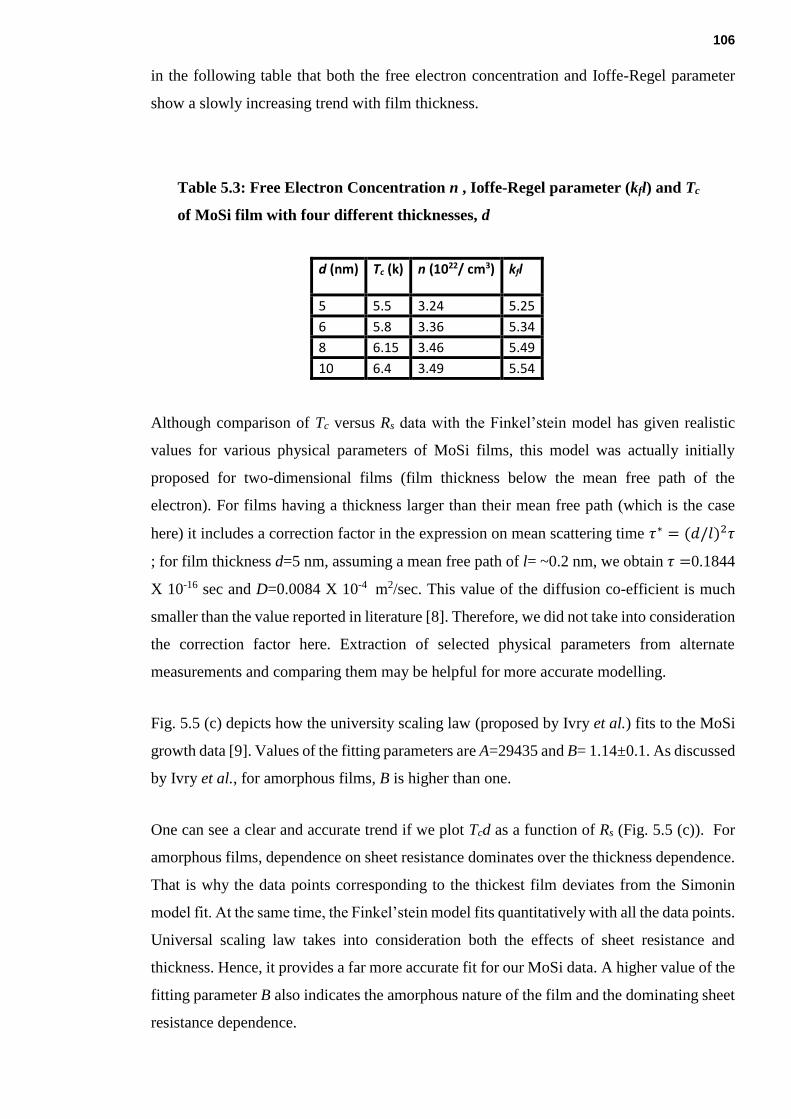
106
in the following table that both the free electron concentration and Ioffe-Regel parameter
show a slowly increasing trend with film thickness.
Although comparison of Tc versus Rs data with the Finkel’stein model has given realistic
values for various physical parameters of MoSi films, this model was actually initially
proposed for two-dimensional films (film thickness below the mean free path of the
electron). For films having a thickness larger than their mean free path (which is the case
here) it includes a correction factor in the expression on mean scattering time 𝜏∗ = (𝑑/𝑙)2𝜏
; for film thickness d=5 nm, assuming a mean free path of l= ~0.2 nm, we obtain 𝜏 =0.1844
X 10-16 sec and D=0.0084 X 10⁻⁴ m2/sec. This value of the diffusion co-efficient is much
smaller than the value reported in literature [8]. Therefore, we did not take into consideration
the correction factor here. Extraction of selected physical parameters from alternate
measurements and comparing them may be helpful for more accurate modelling.
Fig. 5.5 (c) depicts how the university scaling law (proposed by Ivry et al.) fits to the MoSi
growth data [9]. Values of the fitting parameters are A=29435 and B= 1.14±0.1. As discussed
by Ivry et al., for amorphous films, B is higher than one.
One can see a clear and accurate trend if we plot Tcd as a function of Rs (Fig. 5.5 (c)). For
amorphous films, dependence on sheet resistance dominates over the thickness dependence.
That is why the data points corresponding to the thickest film deviates from the Simonin
model fit. At the same time, the Finkel’stein model fits quantitatively with all the data points.
Universal scaling law takes into consideration both the effects of sheet resistance and
thickness. Hence, it provides a far more accurate fit for our MoSi data. A higher value of the
fitting parameter B also indicates the amorphous nature of the film and the dominating sheet
resistance dependence.
Table 5.3: Free Electron Concentration n , Ioffe-Regel parameter (kfl) and Tc
of MoSi film with four different thicknesses, d
d (nm) Tc (k) n (1022/ cm3) kfl
5 5.5 3.24 5.25
6 5.8 3.36 5.34
8 6.15 3.46 5.49
10 6.4 3.49 5.54

107
5.4 Influence of variations in deposition conditions and choice of substrate
We have also explored the effects of various small modifications in the deposition conditions
on the superconducting properties of amorphous MoSi films. Bosworth et al. showed that
substrate cooling may promote amorphous character in superconducting MoSi films and
hence enhance their superconducting characteristics [10]. We have cooled a silicon substrate
under the liquid nitrogen trap (77 K) of our deposition system for three hours and then
immediately deposited a 10 nm thick MoSi film on it. Fig. 5.6 shows that the film deposited
on the cooled substrate has a sheet resistance slightly lower than that of the film deposited
at room temperature. The film deposited on the cooled substrate has a slightly lower Tc
(~0.2K < room temperature deposited film) however the film deposited at a low temperature
shows a sharper superconducting transition (transition width of 55 mK) in comparison to the
film grown at room temperature (376 mK transition width). This narrower transition can be
explained by an improvement in film homogeneity due to deposition on a liquid nitrogen
cooled substrate. In our chamber, the target-substrate distance is large (100 mm). So, there
is unlikely to be significant radiative heating of the substrate holder during deposition.
Hence, even the films we deposited at room temperature are amorphous. (Later on, we
checked this fact using TEM observation.)
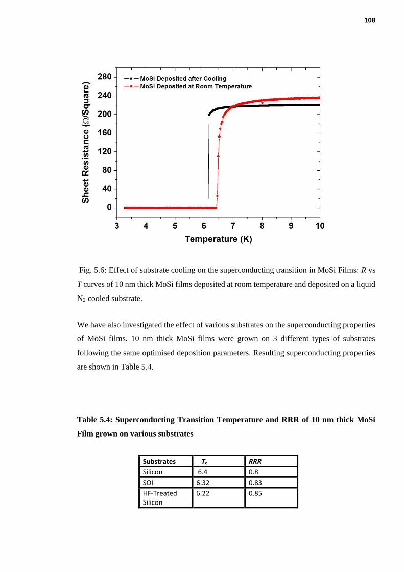
108
Fig. 5.6: Effect of substrate cooling on the superconducting transition in MoSi Films: R vs
T curves of 10 nm thick MoSi films deposited at room temperature and deposited on a liquid
N2 cooled substrate.
We have also investigated the effect of various substrates on the superconducting properties
of MoSi films. 10 nm thick MoSi films were grown on 3 different types of substrates
following the same optimised deposition parameters. Resulting superconducting properties
are shown in Table 5.4.
Table 5.4: Superconducting Transition Temperature and RRR of 10 nm thick MoSi
Film grown on various substrates
Substrates Tc RRR
Silicon 6.4 0.8
SOI 6.32 0.83
HF-Treated Silicon
6.22 0.85
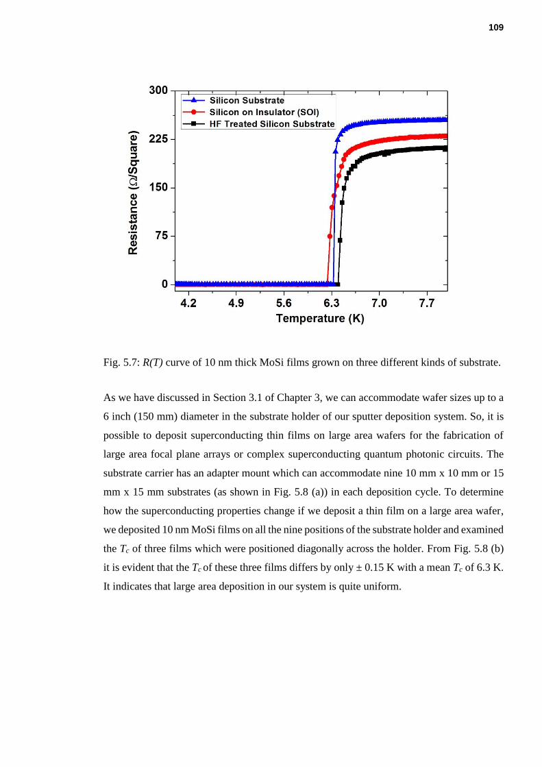
109
Fig. 5.7: R(T) curve of 10 nm thick MoSi films grown on three different kinds of substrate.
As we have discussed in Section 3.1 of Chapter 3, we can accommodate wafer sizes up to a
6 inch (150 mm) diameter in the substrate holder of our sputter deposition system. So, it is
possible to deposit superconducting thin films on large area wafers for the fabrication of
large area focal plane arrays or complex superconducting quantum photonic circuits. The
substrate carrier has an adapter mount which can accommodate nine 10 mm x 10 mm or 15
mm x 15 mm substrates (as shown in Fig. 5.8 (a)) in each deposition cycle. To determine
how the superconducting properties change if we deposit a thin film on a large area wafer,
we deposited 10 nm MoSi films on all the nine positions of the substrate holder and examined
the Tc of three films which were positioned diagonally across the holder. From Fig. 5.8 (b)
it is evident that the Tc of these three films differs by only ± 0.15 K with a mean Tc of 6.3 K.
It indicates that large area deposition in our system is quite uniform.
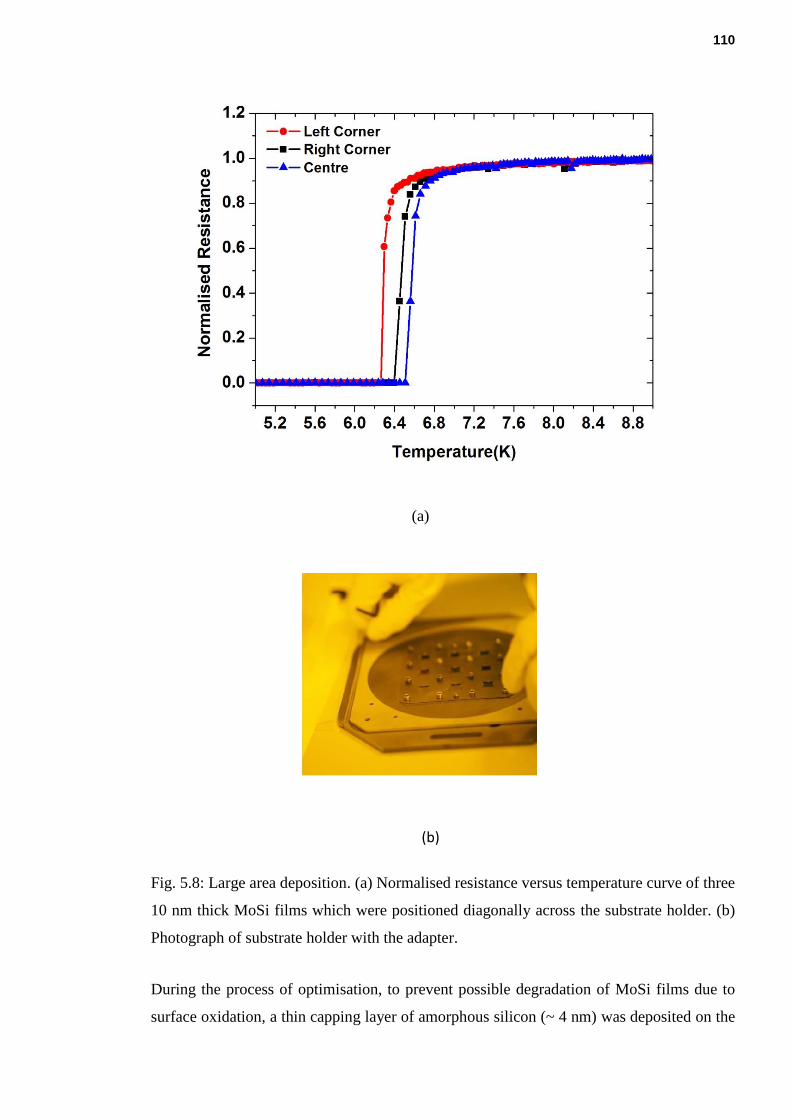
110
(a)
(b)
Fig. 5.8: Large area deposition. (a) Normalised resistance versus temperature curve of three
10 nm thick MoSi films which were positioned diagonally across the substrate holder. (b)
Photograph of substrate holder with the adapter.
During the process of optimisation, to prevent possible degradation of MoSi films due to
surface oxidation, a thin capping layer of amorphous silicon (~ 4 nm) was deposited on the
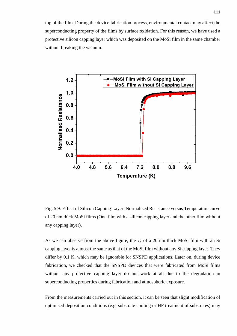
111
top of the film. During the device fabrication process, environmental contact may affect the
superconducting property of the films by surface oxidation. For this reason, we have used a
protective silicon capping layer which was deposited on the MoSi film in the same chamber
without breaking the vacuum.
Fig. 5.9: Effect of Silicon Capping Layer: Normalised Resistance versus Temperature curve
of 20 nm thick MoSi films (One film with a silicon capping layer and the other film without
any capping layer).
As we can observe from the above figure, the Tc of a 20 nm thick MoSi film with an Si
capping layer is almost the same as that of the MoSi film without any Si capping layer. They
differ by 0.1 K, which may be ignorable for SNSPD applications. Later on, during device
fabrication, we checked that the SNSPD devices that were fabricated from MoSi films
without any protective capping layer do not work at all due to the degradation in
superconducting properties during fabrication and atmospheric exposure.
From the measurements carried out in this section, it can be seen that slight modification of
optimised deposition conditions (e.g. substrate cooling or HF treatment of substrates) may
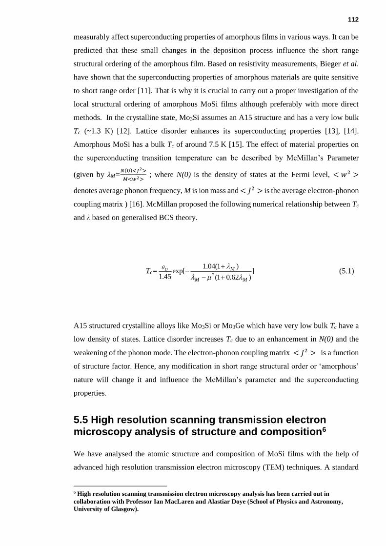
112
measurably affect superconducting properties of amorphous films in various ways. It can be
predicted that these small changes in the deposition process influence the short range
structural ordering of the amorphous film. Based on resistivity measurements, Bieger et al.
have shown that the superconducting properties of amorphous materials are quite sensitive
to short range order [11]. That is why it is crucial to carry out a proper investigation of the
local structural ordering of amorphous MoSi films although preferably with more direct
methods. In the crystalline state, Mo3Si assumes an A15 structure and has a very low bulk
Tc (~1.3 K) [12]. Lattice disorder enhances its superconducting properties [13], [14].
Amorphous MoSi has a bulk Tc of around 7.5 K [15]. The effect of material properties on
the superconducting transition temperature can be described by McMillan’s Parameter
(given by λM=𝑁(0)<𝐽2>
𝑀<𝑤2> ; where N(0) is the density of states at the Fermi level, < 𝑤2 >
denotes average phonon frequency, M is ion mass and < 𝐽2 > is the average electron-phonon
coupling matrix ) [16]. McMillan proposed the following numerical relationship between Tc
and λ based on generalised BCS theory.
Tc= ])62.01(
)1(04.1exp[
45.1 *MM
MD
(5.1)
A15 structured crystalline alloys like Mo3Si or Mo3Ge which have very low bulk Tc have a
low density of states. Lattice disorder increases Tc due to an enhancement in N(0) and the
weakening of the phonon mode. The electron-phonon coupling matrix < 𝐽2 > is a function
of structure factor. Hence, any modification in short range structural order or ‘amorphous’
nature will change it and influence the McMillan’s parameter and the superconducting
properties.
5.5 High resolution scanning transmission electron microscopy analysis of structure and composition6
We have analysed the atomic structure and composition of MoSi films with the help of
advanced high resolution transmission electron microscopy (TEM) techniques. A standard
6 High resolution scanning transmission electron microscopy analysis has been carried out in
collaboration with Professor Ian MacLaren and Alastiar Doye (School of Physics and Astronomy,
University of Glasgow).

113
focussed ion beam (FIB) technique has been used to prepare samples for TEM analysis. The
following figure shows a TEM image (600 KX magnified) of a 5.5 nm thick MoSi film
without a Si capping layer.
Fig. 5.10: Cross section of 5.5 thick MoSi Film without any Si cap.
Fig. 5.11: FFT View of the selected area of the film (marked by a red line in Fig. 5.10).
Silicon Substrate
MoSi Thin Film
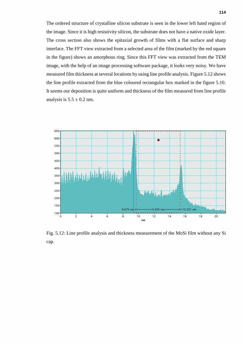
114
The ordered structure of crystalline silicon substrate is seen in the lower left hand region of
the image. Since it is high resistivity silicon, the substrate does not have a native oxide layer.
The cross section also shows the epitaxial growth of films with a flat surface and sharp
interface. The FFT view extracted from a selected area of the film (marked by the red square
in the figure) shows an amorphous ring. Since this FFT view was extracted from the TEM
image, with the help of an image processing software package, it looks very noisy. We have
measured film thickness at several locations by using line profile analysis. Figure 5.12 shows
the line profile extracted from the blue coloured rectangular box marked in the figure 5.10.
It seems our deposition is quite uniform and thickness of the film measured from line profile
analysis is 5.5 ± 0.2 nm.
Fig. 5.12: Line profile analysis and thickness measurement of the MoSi film without any Si
cap.
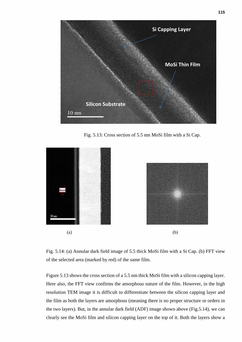
115
Fig. 5.13: Cross section of 5.5 nm MoSi film with a Si Cap.
(a) (b)
Fig. 5.14: (a) Annular dark field image of 5.5 thick MoSi film with a Si Cap. (b) FFT view
of the selected area (marked by red) of the same film.
Figure 5.13 shows the cross section of a 5.5 nm thick MoSi film with a silicon capping layer.
Here also, the FFT view confirms the amorphous nature of the film. However, in the high
resolution TEM image it is difficult to differentiate between the silicon capping layer and
the film as both the layers are amorphous (meaning there is no proper structure or orders in
the two layers). But, in the annular dark field (ADF) image shown above (Fig.5.14), we can
clearly see the MoSi film and silicon capping layer on the top of it. Both the layers show a
MoSi Thin Film
Silicon Substrate
Si Capping Layer
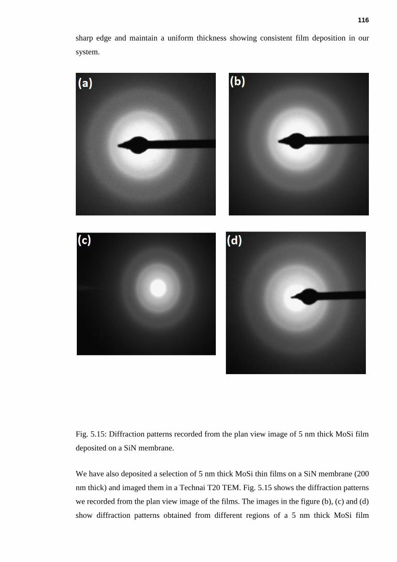
116
sharp edge and maintain a uniform thickness showing consistent film deposition in our
system.
Fig. 5.15: Diffraction patterns recorded from the plan view image of 5 nm thick MoSi film
deposited on a SiN membrane.
We have also deposited a selection of 5 nm thick MoSi thin films on a SiN membrane (200
nm thick) and imaged them in a Technai T20 TEM. Fig. 5.15 shows the diffraction patterns
we recorded from the plan view image of the films. The images in the figure (b), (c) and (d)
show diffraction patterns obtained from different regions of a 5 nm thick MoSi film

117
deposited without any Si capping layer. Figure (a) shows the diffraction pattern when a
selected area aperture is inserted in the TEM. Hence, these images clearly show the
amorphous nature of MoSi film. Our optimised recipe thus promotes the amorphous nature
of MoSi thin films.
As we have stated in Section 5.3, the superconducting properties of amorphous materials
must be very sensitive to short or medium range ordering. We have employed the Fluctuation
Electron Microscopy (FEM) technique to explore local structural ordering of MoSi films.
FEM is a diffraction based analysis to investigate the medium range ordering (~1-3 nm) in
the atomic structure of disordered materials. This method was initially proposed by Gibson
and Treacy [17]. In this technique, a small sample volume was scanned with a probe size of
the order of 1-2 nm, and a large data set of diffraction patterns were collected (thousands of
diffraction patterns). We have carried out this analysis in a JEOL ARM200F microscope
using the Medipix-3 camera. The illumination of the microscope was adjusted by turning the
objective lens off and working in the aberration-corrected Lorentz mode to produce small
probe convergence angles to increase resolution in reciprocal space.
In this analysis, a qualitative idea about short or medium range ordering (SRO/MRO) in the
sample can be achieved from the fluctuations in the diffracted intensity. The magnitude of
such fluctuations is measured by computing the normalised variance of the diffracted
intensity.
𝑉(𝑘𝑠, 𝑟) =<𝐼2(𝑟,𝑘𝑠)>
<𝐼(𝑟,𝑘𝑠)>2 − 1 (5.2)
Here, ks is the scattering vector and r denotes the position in sample space.
In the following figure 5.16, we have shown the diffraction pattern recorded from the MoSi
film. The speckle ring indicates the existence of nano crystalline structures embedded in the
amorphous film. The variance of all the diffraction patterns from the central portion of the
film was calculated as a function of q=2pkr (kr denotes the interplaner distance in reciprocal
lattice space) using the method described by Hart et al. [18]. As we can see in the figure
5.17, the variance plot of the MoSi film has several small and large peaks. A small peak
occurs at a q value of around 1.8 Å-1, while larger peaks are visible at ~2.85 Å-1 and ~4.6 Å-
1. We have compared these peak locations with diffraction peaks of A15 structured Mo3Si
(shown in the same figure). The similarity between them clearly indicates that our films
consist of A15-like nanoscale structures over a short range evolving to a long range disorder.

118
Fig. 5.16: Speckle pattern indicating the existence of short or medium range order in the
MoSi film.
Fig. 5:17: Variance plot of diffracted intensity obtained from the FEM analysis of 5 nm thick
MoSi film, peaks of the variance plot match with the diffraction peak of Mo3Si crystal
structure.
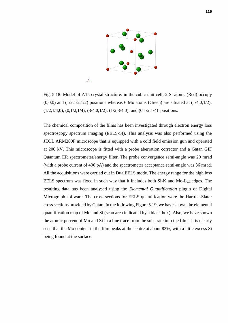
119
Fig. 5.18: Model of A15 crystal structure: in the cubic unit cell, 2 Si atoms (Red) occupy
(0,0,0) and (1/2,1/2,1/2) positions whereas 6 Mo atoms (Green) are situated at (1/4,0,1/2);
(1/2,1/4,0); (0,1/2,1/4); (3/4,0,1/2); (1/2,3/4,0); and (0,1/2,1/4) positions.
The chemical composition of the films has been investigated through electron energy loss
spectroscopy spectrum imaging (EELS-SI). This analysis was also performed using the
JEOL ARM200F microscope that is equipped with a cold field emission gun and operated
at 200 kV. This microscope is fitted with a probe aberration corrector and a Gatan GIF
Quantum ER spectrometer/energy filter. The probe convergence semi-angle was 29 mrad
(with a probe current of 400 pA) and the spectrometer acceptance semi-angle was 36 mrad.
All the acquisitions were carried out in DualEELS mode. The energy range for the high loss
EELS spectrum was fixed in such way that it includes both Si-K and Mo-L2,3 edges. The
resulting data has been analysed using the Elemental Quantification plugin of Digital
Micrograph software. The cross sections for EELS quantification were the Hartree-Slater
cross sections provided by Gatan. In the following Figure 5.19, we have shown the elemental
quantification map of Mo and Si (scan area indicated by a black box). Also, we have shown
the atomic percent of Mo and Si in a line trace from the substrate into the film. It is clearly
seen that the Mo content in the film peaks at the centre at about 83%, with a little excess Si
being found at the surface.
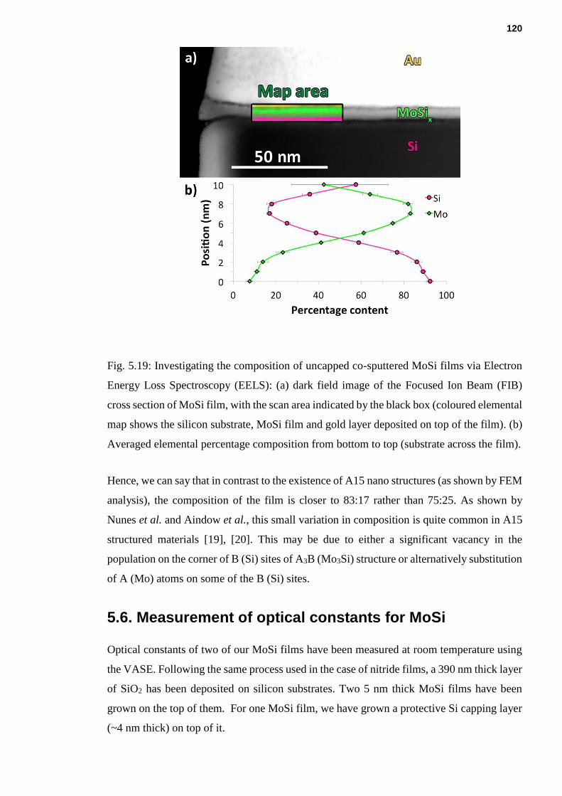
120
Fig. 5.19: Investigating the composition of uncapped co-sputtered MoSi films via Electron
Energy Loss Spectroscopy (EELS): (a) dark field image of the Focused Ion Beam (FIB)
cross section of MoSi film, with the scan area indicated by the black box (coloured elemental
map shows the silicon substrate, MoSi film and gold layer deposited on top of the film). (b)
Averaged elemental percentage composition from bottom to top (substrate across the film).
Hence, we can say that in contrast to the existence of A15 nano structures (as shown by FEM
analysis), the composition of the film is closer to 83:17 rather than 75:25. As shown by
Nunes et al. and Aindow et al., this small variation in composition is quite common in A15
structured materials [19], [20]. This may be due to either a significant vacancy in the
population on the corner of B (Si) sites of A3B (Mo3Si) structure or alternatively substitution
of A (Mo) atoms on some of the B (Si) sites.
5.6. Measurement of optical constants for MoSi
Optical constants of two of our MoSi films have been measured at room temperature using
the VASE. Following the same process used in the case of nitride films, a 390 nm thick layer
of SiO2 has been deposited on silicon substrates. Two 5 nm thick MoSi films have been
grown on the top of them. For one MoSi film, we have grown a protective Si capping layer
(~4 nm thick) on top of it.
121
In the following figure 5.20, we have shown the optical constants evaluated from a 5 nm
thick MoSi film and a 5 nm film thick MoSi film with a Si capping layer. The presence of
the Si capping layer slightly enhances the extinction co-efficient. The enhancement of
absorption co-efficient due to the Si capping layer is more pronounced at λ< 600 nm. This
wavelength range is well above the gap energy of Si, so the Si is acting as an additional
absorbing layer. Over the IR range, a slight enhancement in k for the Si capping is still
noticeable. We have also compared these measurements with VASE measurements carried
out on 5.5 nm thick polycrystalline NbN and NbTiN thin films. It can be easily seen that
MoSi films have a much higher extinction coefficient (k) in comparison to NbN or NbTiN
over the whole spectral range, which means that at any specific wavelength the MoSi thin
films are more favourable in terms of optical absorption. We can also see that the k(λ) curve
of MoSi shows a continuous sharp increase even in the higher wavelength region (1500nm
-2200nm). But for NbN or NbTiN, k(λ) shows a saturation and very slow increment in that
wavelength region. Hence, MoSi can serve as a more suitable material for mid-infrared
SNSPDs in terms of optical properties.
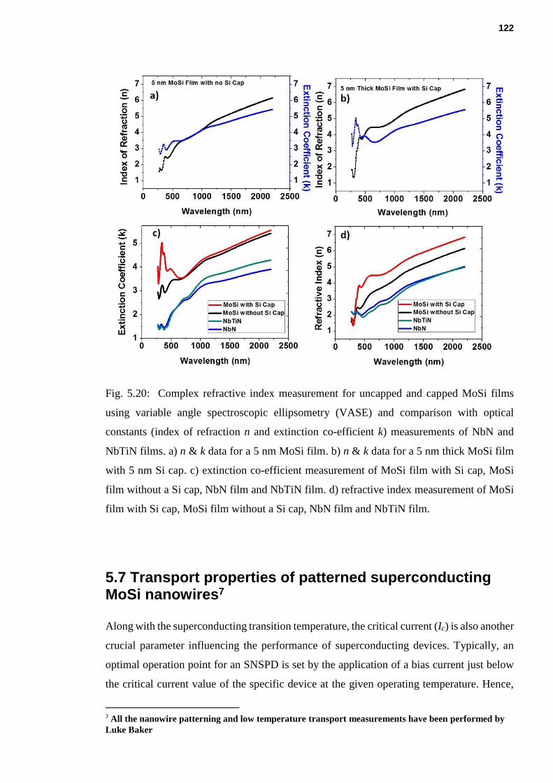
122
Fig. 5.20: Complex refractive index measurement for uncapped and capped MoSi films
using variable angle spectroscopic ellipsometry (VASE) and comparison with optical
constants (index of refraction n and extinction co-efficient k) measurements of NbN and
NbTiN films. a) n & k data for a 5 nm MoSi film. b) n & k data for a 5 nm thick MoSi film
with 5 nm Si cap. c) extinction co-efficient measurement of MoSi film with Si cap, MoSi
film without a Si cap, NbN film and NbTiN film. d) refractive index measurement of MoSi
film with Si cap, MoSi film without a Si cap, NbN film and NbTiN film.
5.7 Transport properties of patterned superconducting MoSi nanowires7
Along with the superconducting transition temperature, the critical current (Ic) is also another
crucial parameter influencing the performance of superconducting devices. Typically, an
optimal operation point for an SNSPD is set by the application of a bias current just below
the critical current value of the specific device at the given operating temperature. Hence,
7 All the nanowire patterning and low temperature transport measurements have been performed by
Luke Baker
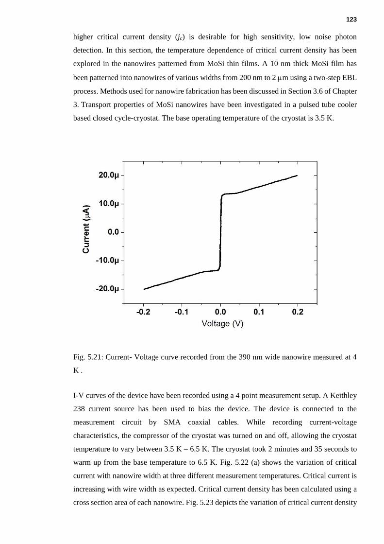
123
higher critical current density (jc) is desirable for high sensitivity, low noise photon
detection. In this section, the temperature dependence of critical current density has been
explored in the nanowires patterned from MoSi thin films. A 10 nm thick MoSi film has
been patterned into nanowires of various widths from 200 nm to 2 m using a two-step EBL
process. Methods used for nanowire fabrication has been discussed in Section 3.6 of Chapter
3. Transport properties of MoSi nanowires have been investigated in a pulsed tube cooler
based closed cycle-cryostat. The base operating temperature of the cryostat is 3.5 K.
Fig. 5.21: Current- Voltage curve recorded from the 390 nm wide nanowire measured at 4
K .
I-V curves of the device have been recorded using a 4 point measurement setup. A Keithley
238 current source has been used to bias the device. The device is connected to the
measurement circuit by SMA coaxial cables. While recording current-voltage
characteristics, the compressor of the cryostat was turned on and off, allowing the cryostat
temperature to vary between 3.5 K – 6.5 K. The cryostat took 2 minutes and 35 seconds to
warm up from the base temperature to 6.5 K. Fig. 5.22 (a) shows the variation of critical
current with nanowire width at three different measurement temperatures. Critical current is
increasing with wire width as expected. Critical current density has been calculated using a
cross section area of each nanowire. Fig. 5.23 depicts the variation of critical current density
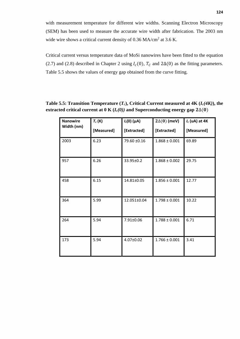
124
with measurement temperature for different wire widths. Scanning Electron Microscopy
(SEM) has been used to measure the accurate wire width after fabrication. The 2003 nm
wide wire shows a critical current density of 0.36 MA/cm2 at 3.6 K.
Critical current versus temperature data of MoSi nanowires have been fitted to the equation
(2.7) and (2.8) described in Chapter 2 using 𝐼𝑐(0), 𝑇𝐶 and 2∆(0) as the fitting parameters.
Table 5.5 shows the values of energy gap obtained from the curve fitting.
Table 5.5: Transition Temperature (Tc), Critical Current measured at 4K (Ic(4K)), the
extracted critical current at 0 K (Ic(0)) and Superconducting energy gap 𝟐∆(𝟎)
Nanowire Width (nm)
Tc (K)
[Measured]
Ic(0) (µA)
[Extracted]
𝟐∆(𝟎) (meV)
[Extracted]
Ic (uA) at 4K
[Measured]
2003
6.23
79.60 ±0.16
1.868 ± 0.001 69.89
957
6.26
33.95±0.2
1.868 ± 0.002 29.75
458
6.15 14.81±0.05
1.856 ± 0.001 12.77
364
5.99
12.051±0.04
1.798 ± 0.001 10.22
264
5.94
7.91±0.06
1.788 ± 0.001 6.71
173 5.94 4.07±0.02
1.766 ± 0.001 3.41
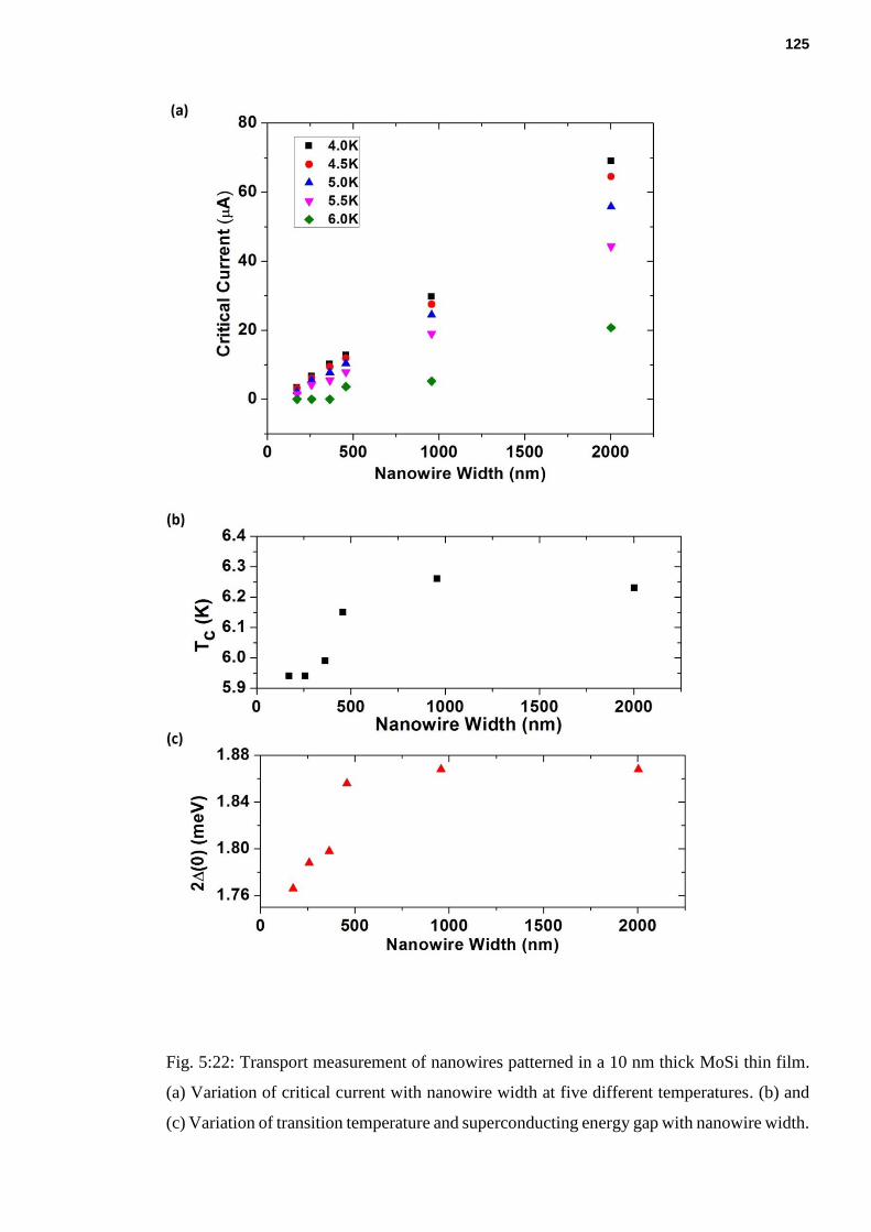
125
Fig. 5:22: Transport measurement of nanowires patterned in a 10 nm thick MoSi thin film.
(a) Variation of critical current with nanowire width at five different temperatures. (b) and
(c) Variation of transition temperature and superconducting energy gap with nanowire width.

126
It is evident that all the nanowires (2003-173 nm width) show a similar trend of
superconducting transport properties. Tc is slightly depressed with decreasing wire width
(from 6.23 K to 5.94 K). Fig. 5.22 (b) and 5.22 (c) demonstrate how Tc and the values of
superconducting energy gap obtained through the curve fitting vary over the nanowire width.
Though critical current decreases consistently with wire width (as expected), all the
nanowires show a common trend of variation in critical current density with temperature
(Fig. 5.23). Also, at any specific measurement temperature, there is a slow reduction in
critical current density values of the nanowires with decreasing wire width. The nanowire of
2003 nm width shows a critical current density of 0.36 MA/cm2 measured at 3.6 K. The
thinnest nanowire (173 nm wide) shows a comparatively lower Jc of 0.2 MA/cm2. This
deviation along with the fluctuation in values of Jc in the rest of the nanowires can be
explained by inhomogeneity caused during the nanowire fabrication. Close SEM inspection
indicates the edges of the nanowires may be damaged with redeposition of etch debris and
e-beam resist which would lead to a reduction in the superconducting cross section. This
effect would be strongest (proportionately to the width) in the narrowest wires. The
superconducting energy gaps of the nanowires based on our thin films are much smaller than
the bulk energy gap of MoSi (~ 2.26 meV) reported in the literature. The wire width > 458
nm 2Δ(0) assumes a value of ~ 1.87 meV; for the 173 nm wide nanowire, it drops to 1.77
meV.
127
Fig. 5.23: Critical current density versus temperature curve of MoSi nanowires with widths
ranging from 90 nm to 2003 nm (widths of the nanowires have been corrected from SEM
inspection).
Lita et al. [15] have reported a critical current density of ~1.3 MA/cm2 at 250 mK for a 1μm
wide nanowire patterned on a 6.3 nm thick MoSi film. Korneeva et al. [21], [22] have shown
critical current density varies from 1.1-2.5 MA/cm2 for nanowire patterned meander devices
on 4 nm thick MoSi films measured at 1.7 K. In comparison, the lower critical current
densities observed in the nanowires fabricated from our film can be explained by a higher
measurement temperature range.
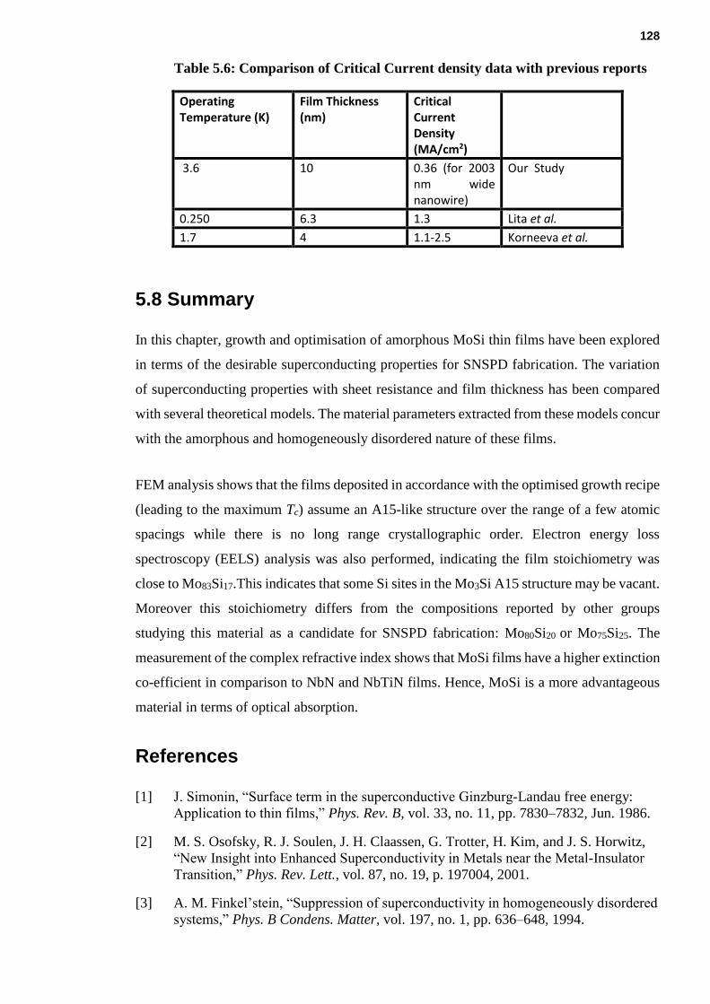
128
Table 5.6: Comparison of Critical Current density data with previous reports
Operating Temperature (K)
Film Thickness (nm)
Critical Current Density (MA/cm2)
3.6 10 0.36 (for 2003 nm wide nanowire)
Our Study
0.250 6.3 1.3 Lita et al.
1.7 4 1.1-2.5 Korneeva et al.
5.8 Summary
In this chapter, growth and optimisation of amorphous MoSi thin films have been explored
in terms of the desirable superconducting properties for SNSPD fabrication. The variation
of superconducting properties with sheet resistance and film thickness has been compared
with several theoretical models. The material parameters extracted from these models concur
with the amorphous and homogeneously disordered nature of these films.
FEM analysis shows that the films deposited in accordance with the optimised growth recipe
(leading to the maximum Tc) assume an A15-like structure over the range of a few atomic
spacings while there is no long range crystallographic order. Electron energy loss
spectroscopy (EELS) analysis was also performed, indicating the film stoichiometry was
close to Mo83Si17.This indicates that some Si sites in the Mo3Si A15 structure may be vacant.
Moreover this stoichiometry differs from the compositions reported by other groups
studying this material as a candidate for SNSPD fabrication: Mo80Si20 or Mo75Si25. The
measurement of the complex refractive index shows that MoSi films have a higher extinction
co-efficient in comparison to NbN and NbTiN films. Hence, MoSi is a more advantageous
material in terms of optical absorption.
References
[1] J. Simonin, “Surface term in the superconductive Ginzburg-Landau free energy:
Application to thin films,” Phys. Rev. B, vol. 33, no. 11, pp. 7830–7832, Jun. 1986.
[2] M. S. Osofsky, R. J. Soulen, J. H. Claassen, G. Trotter, H. Kim, and J. S. Horwitz,
“New Insight into Enhanced Superconductivity in Metals near the Metal-Insulator
Transition,” Phys. Rev. Lett., vol. 87, no. 19, p. 197004, 2001.
[3] A. M. Finkel’stein, “Suppression of superconductivity in homogeneously disordered
systems,” Phys. B Condens. Matter, vol. 197, no. 1, pp. 636–648, 1994.
129
[4] J. M. Graybeal and M. R. Beasley, “Localization and interaction effects in ultrathin
amorphous superconducting films,” Phys. Rev. B, vol. 29, no. 7, pp. 4167–4169,
Apr. 1984.
[5] A. Semenov, B. Günther, U. Böttger, H.-W. Hübers, H. Bartolf, A. Engel, A.
Schilling, K. Ilin, M. Siegel, R. Schneider, D. Gerthsen, and N. A. Gippius, “Optical
and transport properties of ultrathin NbN films and nanostructures,” Phys. Rev. B,
vol. 80, no. 5, p. 54510, Aug. 2009.
[6] N. Hadacek, M. Sanquer, and J.-C. Villé, “Double reentrant superconductor-
insulator transition in thin TiN films,” Phys. Rev. B, vol. 69, p. 24505, 2004.
[7] M. R. Graham, C. J. Adkins, H. Behar, and R. Rosenbaum, “Experimental study of
the Ioffe-Regel criterion for amorphous indium oxide films,” J. Phys. Condens.
Matter, vol. 10, no. 4, pp. 809–819, Feb. 1998.
[8] X. Zhang, A. Engel, Q. Wang, A. Schilling, A. Semenov, M. Sidorova, H.-W.
Hübers, I. Charaev, K. Ilin, and M. Siegel, “Characteristics of superconducting
tungsten silicide W x Si1−x for single photon detection,” Phys. Rev. B, vol. 94, 2016.
[9] Y. Ivry, C. S. Kim, A. E. Dane, D. De Fazio, A. N. McCaughan, K. A. Sunter, Q.
Zhao, and K. K. Berggren, “Universal scaling of the critical temperature for thin
films near the superconducting-to-insulating transition,” Phys. Rev. B, vol. 90, no.
21, p. 214515, 2014.
[10] D. Bosworth, S.-L. Sahonta, R. H. Hadfield, and Z. H. Barber, “Amorphous
Molybdenum Silicon Superconducting Thin Films,” AIP Adv., vol. 5, no. 8, p.
87106, 2015.
[11] J. Bieger, H. Adrian, P. Müller, G. Saemann-Ischenko, and E. L. Haase,
“Superconductivity and electrical resistivity of amorphous Nb75Ge25 and
Nb80Si20 after heavy ion irradiation at low temperature,” Solid State Commun., vol.
36, no. 11, pp. 979–982, 1980.
[12] H. M. Tütüncü, S. Bağcı, and G. P. Srivastava, “Electronic structure, phonons, and
electron-phonon interaction in Mo 3 Si,” Phys. Rev. B, vol. 82, no. 21, p.
214510, Dec. 2010.
[13] M. Lehmann, G. Saemann-Ischenko, H. Adrian, and C. Nölscher, “Disordered A15
compounds from the Matthias-Valley: Mo3Ge and Mo3Si,” Phys. B+C, vol. 107, no.
1, pp. 473–474, 1981.
[14] A. E. Kar’kin, V. I. Voronin, T. V. D’yachkova, N. I. Kadyrova, A. P. Tyutyunik,
V. G. Zubkov, Y. G. Zainulin, M. V. Sadovskii, and B. N. Goshchitskii,
“Superconducting properties of the atomically disordered MgB2 compound,” J. Exp.
Theor. Phys. Lett., vol. 73, no. 10, pp. 570–572, 2001.
[15] A. E. Lita, V. B. Verma, R. D. Horansky, J. M. Shainline, R. P. Mirin, and S. Nam,
“Materials Development for High Efficiency Superconducting Nanowire Single-
Photon Detectors,” MRS Proc., vol. 1807, pp. 1–6, 2015.
[16] W. L. McMillan, “Transition Temperature of Strong-Coupled Superconductors,”
Phys. Rev., vol. 167, no. 2, pp. 331–344, Mar. 1968.
[17] M. M. J. Treacy and J. M. Gibson, “Variable coherence microscopy,” Acta
Crystallogr. Sect. A Found. Crystallogr., vol. 52, no. 2, pp. 212–220, 1996.

130
[18] R. Bassiri, M. Hart, R. L. Byer, K. B. Borisenko, K. Evans, M. M. Fejer, A. C. Lin,
I. MacLaren, A. S. Markosyan, I. W. Martin, R. K. Route, and S. Rowan,
“Investigating the medium range order in amorphous Ta2 O5 coatings,” J. Phys.
Conf. Ser., vol. 522, no. June, p. 12043, 2014.
[19] C. A. Nunes, G. C. Coelho, and A. S. Ramos, “On the invariant reactions in the Mo-
rich portion of the Mo-Si system,” J. Phase Equilibria, vol. 22, no. 5, pp. 556–559,
Oct. 2001.
[20] M. Aindow, L. S. Smith, J. Shyue, M. H. Loretto, and H. L. Fraser, “On the origins
of ‘forbidden’ 100-type spots in electron diffraction patterns from the A15
compounds Nb 3 AI, Cr 3 Si and V 3 Si,” Philos. Mag. Lett., vol. 69, no. 1, pp. 23–
30, Jan. 1994.
[21] Y. P. Korneeva, M. Y. Mikhailov, and Y. P. Pershin, “Superconducting single-
photon detector made of MoSi film,” arXiv:1309.7074v1.
[22] Y. P. Korneeva, M. Y. Mikhailov, Y. P. Pershin, N. N. Manova, A. V Divochiy, Y.
B. Vakhtomin, A. A. Korneev, K. V Smirnov, A. G. Sivakov, A. Y. Devizenko, and
G. N. Goltsman, “Superconducting single-photon detector made of MoSi film,”
Supercond. Sci. Technol., vol. 27, no. 9, p. 95012, Sep. 2014.
131
Chapter 6
Titanium nitride (TiN) Growth for Microwave
Kinetic Inductance Detector Applications
Microwave Kinetic Inductance Detector (MKID) is a cryogenic detector technology which
is quickly gaining importance in the field of astronomical instruments. The main advantages
of MKIDs are that they are simple to fabricate and easy to multiplex into a large detector
array using the concept of frequency domain multiplexing [1]. As stated in Section 2.6 of
Chapter 2, basic operating principle of any MKID device is to measure the change in the
complex impedance of the superconducting film upon photon absorption. Any photon with
an energy of h𝜈 >2Δ if absorbed will break the Cooper pairs resulting in an increase in the
kinetic inductance (Lk). This change in Lk is very small; so we need to pattern the
superconducting films in to a high quality factor microwave resonance circuit to detect this
variation.
Traditionally, MKIDs have been fabricated into superconducting quarter-wavelength or
half-wavelength resonator elements capacitive coupled to a co-planar feed line. The change
in kinetic inductance is detected from the resulting shift in the resonant frequency of the
resonant circuit. This approach requires the quasi-particles generated by photon absorption
to be concentrated at the high current density region of the circuit. This can be achieved by
antenna coupling or quasi-particle trapping. For the detectors to work at a terahertz
frequency range (approximately 0.3 to 3 THz or 1 mm to 100 µm in terms of wavelength),
where antenna coupling can introduce a significant loss of efficiency, then a direct
absorption method needs to be considered. The concept of Lumped Element KID (LEKID)
has been proposed to solve this problem of coupling terahertz radiation to kinetic inductance
detectors. In this design, there is no requirement of antenna coupling or quasi-particle
trapping [2], [3].
We have explored the potential of TiN as an alternate base material for superconducting
lumped element kinetic inductance detector (LEKID) fabrication. Titanium nitride (TiN) has
been demonstrated to work as a useful material for MKIDs [4]. It offers several advantages
over the more traditionally available material (e.g. Al) for this purpose. The superconducting
property of TiN is tuneable with the nitrogen content of the film. So, we can engineer
detector material accordingly to our need. TiN also has higher normal state resistivity. There

132
is less possibility of formation of surface oxide on the top of TiN film. Moreover, due to its
higher Tc, TiN based MKID devices can be operated at a comparatively higher base
temperature which is within the reach of modern close cycle cryogenic cooling technology.
6.1 Optimisation of TiN thin film growth in sputter deposition system
TiN thin films have been grown by reactive sputtering (Chapter 3.1.1). Double sized
polished high resistivity silicon wafers have been used as substrates for this purpose. TiN
films are deposited by the sputtering of Ti targets and by introducing a small amount of
nitrogen into the chamber as the reacting gas. The distance between the substrate and the
target is kept at 100 mm. We introduced 18 sccm of argon into the chamber with a fixed
position of the throttle valve (75°). The following Fig. 6.1 shows the R versus T curve of 90
nm thick TiN film grown with several nitrogen flows. It can be seen that a Tc of 2.9 K can
be achieved if we grow the film with a 10 sccm N2 flow. When the substrate is heated up to
500°C before deposition, a 4 K Tc can be achieved. For these deposition parameters, a
deposition time of 40 minutes was required to grow the 90 nm thick films (meaning the
deposition rate was 2.25 nm/minute). Before deposition, we have cleaned the substrates in an
ultrasonic bath with RO water, acetone and IPA for 5 minutes. Also, the substrates have been
etched with diluted hydro fluoric (HF) acid immediately prior to film growth in order to remove
the native silicon oxide layer grown on the top of the substrate. The film grown on the heated
substrate has less sheet resistance indicating a larger grain size and improved structural property
of the film grown at higher temperature.
Table 6.1 Recipe used for sputtered TiN growth
Ti: 0.6 A (238 W, 397 V when deposited at room temperature; 242 W, 404 V after heating substrate)
Ar Flow 18 sccm
Total Pressure 0.18 Pa
Target Substrate Distance 100 mm
Substrate Holder Rotation 60 rpm
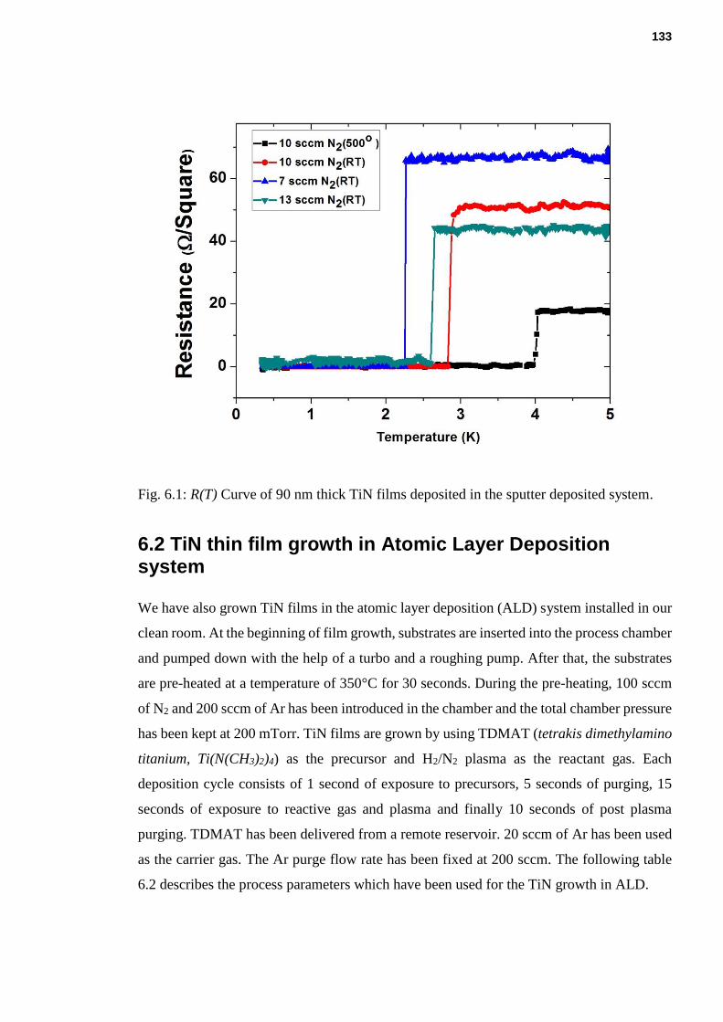
133
Fig. 6.1: R(T) Curve of 90 nm thick TiN films deposited in the sputter deposited system.
6.2 TiN thin film growth in Atomic Layer Deposition system
We have also grown TiN films in the atomic layer deposition (ALD) system installed in our
clean room. At the beginning of film growth, substrates are inserted into the process chamber
and pumped down with the help of a turbo and a roughing pump. After that, the substrates
are pre-heated at a temperature of 350°C for 30 seconds. During the pre-heating, 100 sccm
of N2 and 200 sccm of Ar has been introduced in the chamber and the total chamber pressure
has been kept at 200 mTorr. TiN films are grown by using TDMAT (tetrakis dimethylamino
titanium, Ti(N(CH3)2)4) as the precursor and H2/N2 plasma as the reactant gas. Each
deposition cycle consists of 1 second of exposure to precursors, 5 seconds of purging, 15
seconds of exposure to reactive gas and plasma and finally 10 seconds of post plasma
purging. TDMAT has been delivered from a remote reservoir. 20 sccm of Ar has been used
as the carrier gas. The Ar purge flow rate has been fixed at 200 sccm. The following table
6.2 describes the process parameters which have been used for the TiN growth in ALD.

134
Table 6.2 Recipe used for TiN growth in Atomic Layer Deposition (ALD)
Pre-Heat (at 350oC) 100 sccm N2 , 200 sccm Ar Purge; Chamber Pressure: 200 mTorr Duration: 30 seconds
Pressure Set up
TDMAT Dose 200 sccm Ar Purge, 20 sccm Ar Carrier; Chamber Pressure: 40 mTorr Duration: 1 seconds
TDMAT Purge 200 Sccm Ar Purge, 20 Sccm Ar Carrier; Chamber Pressure: 40 mTorr Duration: 5 seconds
Plasma Gas stabilisation 5 sccm H2, 15 or 30 sccm N2, 200 sccm Ar Purge, 20 sccm Ar Carrier; Chamber Pressure: 10 mTorr Duration: 5 seconds
H2/N2 Plasma 5 sccm H2, 30 or 15 sccm N2, 200 sccm Ar Purge, 20 sccm Ar Carrier; Chamber Pressure: 10 mTorr Duration: 5 seconds Plasma Power: 200 W Duration: 15 seconds
Post Plasma Purge 200 sccm Ar Purge, 200 sccm Ar Carrier; Chamber Pressure: 40 mTorr Duration: 10 seconds

135
Fig. 6.2: R(T) Curve of 30 nm thick TiN films deposited in the atomic layer deposition
system (Nitrogen flow rate in the reactive plasma has been varied).
Fig. 6.2 presents the Tc measurement of the 30 nm thick TiN films deposited following the
process described in Table 6.2. Two different N2 flow rates in the reactive plasma have been
used during TiN film growth. As it can be seen from the above figure, for the film grown
with 30 sccm N2, a 2.4 K Tc can be obtained. In this recipe, a total of 240 minutes (4 hours)
of deposition time was used to grow a 30 nm thick TiN film (meaning the film deposition
rate was 0.125 nm/minute).
A set of thicker TiN film (60 nm) grown by the ALD process have shown reduced Tc (2.2
K) which is contrary to the common trend found in the literature for TiN films [5]. This
anomalous behaviour may be explained by growth of impurities from the precursor in the
film as the film thickness is increased, degrading the superconducting properties.
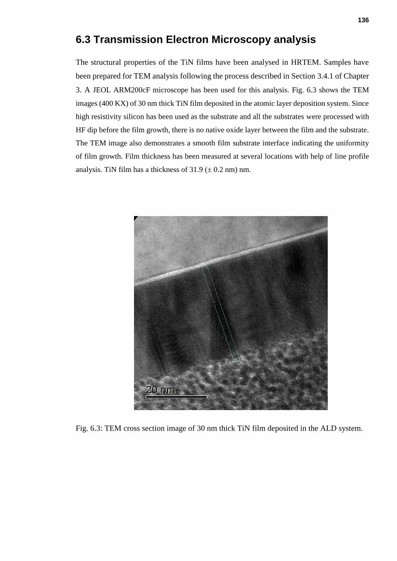
136
6.3 Transmission Electron Microscopy analysis
The structural properties of the TiN films have been analysed in HRTEM. Samples have
been prepared for TEM analysis following the process described in Section 3.4.1 of Chapter
3. A JEOL ARM200cF microscope has been used for this analysis. Fig. 6.3 shows the TEM
images (400 KX) of 30 nm thick TiN film deposited in the atomic layer deposition system. Since
high resistivity silicon has been used as the substrate and all the substrates were processed with
HF dip before the film growth, there is no native oxide layer between the film and the substrate.
The TEM image also demonstrates a smooth film substrate interface indicating the uniformity
of film growth. Film thickness has been measured at several locations with help of line profile
analysis. TiN film has a thickness of 31.9 (± 0.2 nm) nm.
Fig. 6.3: TEM cross section image of 30 nm thick TiN film deposited in the ALD system.
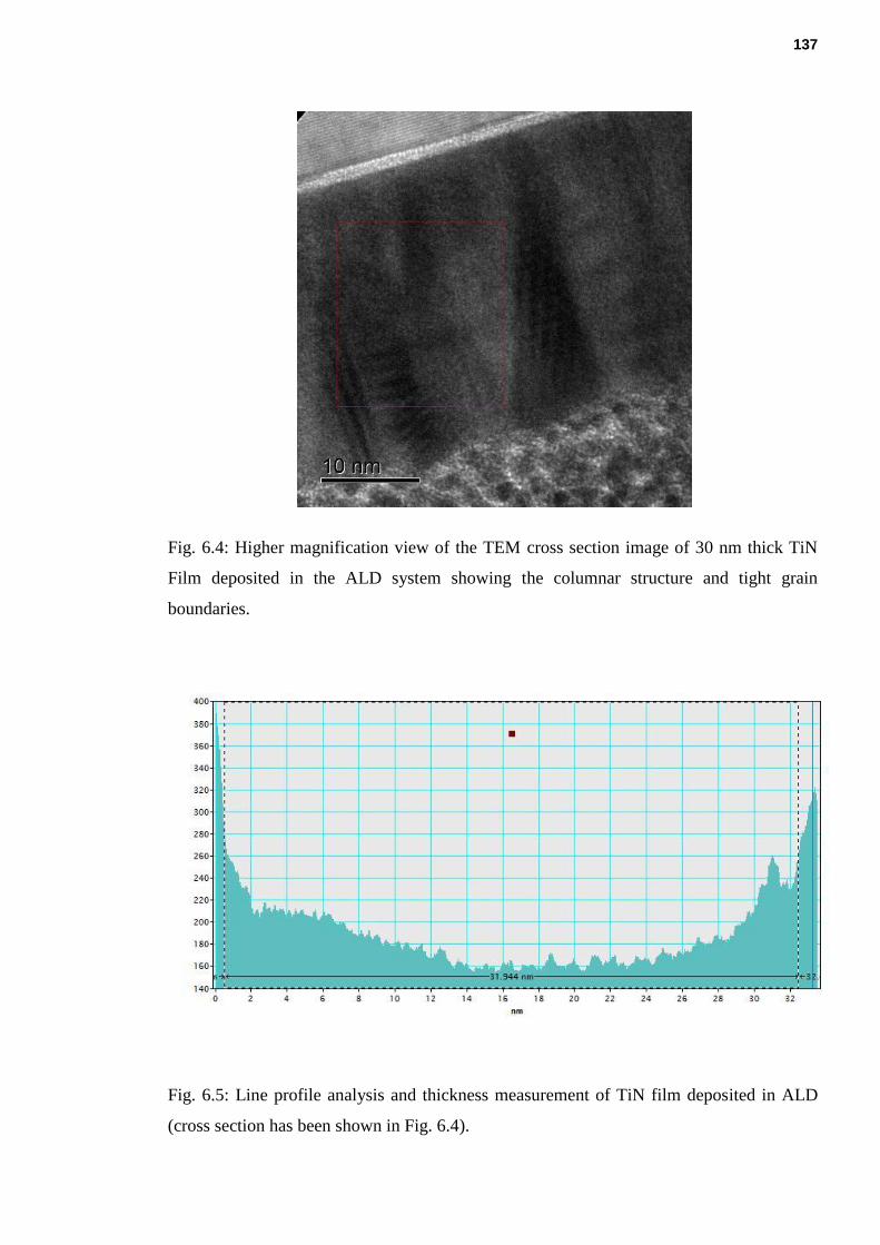
137
Fig. 6.4: Higher magnification view of the TEM cross section image of 30 nm thick TiN
Film deposited in the ALD system showing the columnar structure and tight grain
boundaries.
Fig. 6.5: Line profile analysis and thickness measurement of TiN film deposited in ALD
(cross section has been shown in Fig. 6.4).

138
(a) (b)
Fig. 6.6: Structural properties of ALD deposited TiN film: (a) FFT view extracted from the
area marked by the red square in Fig. 6.5; (b) Convergent beam electron diffraction image
of the TiN film.
Both Fig. 6.3 and Fig. 6.4 show columnar film growth and tight grain boundaries (grains
have a horizontal dimension of ~ 15 -20 nm). In Fig. 6.6 (a), an FFT view extracted from the
area marked by the red square in Fig. 6.4 has been shown. Though the image is very noisy,
the existence of structural order can be seen. In Fig. 6.6 (b), we have shown a convergent
beam electron diffraction pattern recorded the TiN film. Fig. 6.7 shows a cross section image
of 90 nm thick TiN film grown on a heated substrate in the sputter deposition system. The
line profile indicates a thickness of 87.5± 0.3 nm. The crystalline structure and large grains
of the sputter deposited film can be observed from the TEM image.

139
Fig. 6.7: TEM cross section image of 90 nm thick TiN Film deposited in the sputter
deposition system.
Fig. 6.8: Line profile analysis and thickness measurement of TiN film deposited in the
sputter system (cross section has been shown in Fig. 6.7).
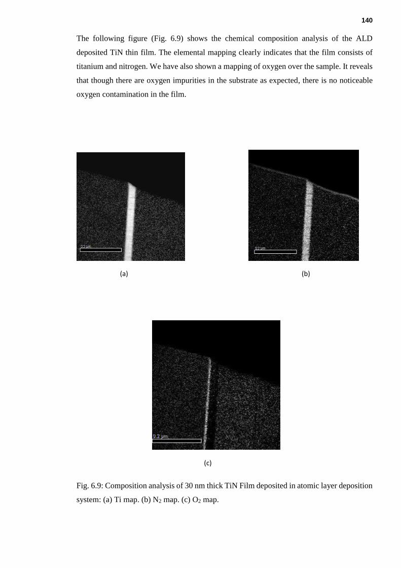
140
The following figure (Fig. 6.9) shows the chemical composition analysis of the ALD
deposited TiN thin film. The elemental mapping clearly indicates that the film consists of
titanium and nitrogen. We have also shown a mapping of oxygen over the sample. It reveals
that though there are oxygen impurities in the substrate as expected, there is no noticeable
oxygen contamination in the film.
(a) (b)
(c)
Fig. 6.9: Composition analysis of 30 nm thick TiN Film deposited in atomic layer deposition
system: (a) Ti map. (b) N2 map. (c) O2 map.

141
6.4 Device fabrication and testing8
MKID devices have been fabricated based on the TiN thin films deposited following the
optimised recipes described in this chapter. The device fabricated based on the 90 nm thick
sputter deposited film showed a resonance. However, the resonance curve of the device was
unresponsive to any optical radiation. On the other hand, the device fabricated from 30 nm
thick ALD deposited film has shown a proper response. As shown in the following figure,
the resonant frequency of the MKID device shifts towards left with the increase in optical
power while the depth of the resonance decreases. Fig. 6.10 demonstrates the design and the
optical microscope image of the device.
Fig. 6.10: Design and optical microscope image of the MKID device fabricated from the 30
nm thick ALD deposited TiN film.
8 MKID device fabrication and low temperature characterisation have been performed by Dr. Dmtry
Morozov using facilities at the University of Cardiff.

142
Fig. 6.11: Low temperature characterisation of the MKID device: (a) Resonance curve of the
device with different blackbody radiation. (b) Optical NEP of the phase response of the
device at Tbase = 230 mK.
(a)
(b)

143
From the Fig. 6.11 (a), it is clear that the device is responsive to blackbody radiation. At the
lowest blackbody temperature (8.16 K), the resonant frequency of the device is 2.0812 GHz.
The internal quality factor of the device is 21783.22. Base temperature of the device is
maintained below 0.3 K. Fig. 6.11 (b) shows optical NEP data of phase response of the
device at a 350 mK temperature. It is of the order of ~10^-15. As stated in Chapter 2, this
NEP value is sufficient for the application in passive terahertz imaging.
6.5 Summary
In this chapter, optimisation of TiN thin film growth for MKID applications has been
reported. 30 nm thick ALD deposited film has shown a Tc of 2.4 K and 90 nm thick sputter
deposited film has shown a maximum Tc of 4 K. The deposition rate of the ALD process is
much slower (~18 times) in comparison to the sputter deposition. HRTEM analysis reveals
that TiN films are highly crystalline in nature with large grain size. A prototype MKID
device has been fabricated from the TiN film that was grown following recipes described in
this chapter. The difference in the optical response of devices fabricated from the sputtered
and ALD deposited films is still unknown, but a slower deposition rate and higher uniformity
of ALD films can be a crucial reason behind this.
References
[1] P. K. Day, H. G. LeDuc, B. A. Mazin, A. Vayonakis, and J. Zmuidzinas, “A
broadband superconducting detector suitable for use in large arrays,” Nature, vol.
425, no. 6960, pp. 817–821, Oct. 2003.
[2] S. Doyle, P. Mauskopf, J. Naylon, A. Porch, and C. Duncombe, “Lumped Element
Kinetic Inductance Detectors,” J. Low Temp. Phys., vol. 151, no. 1–2, pp. 530–536,
Apr. 2008.
[3] S. Rowe, “Passive terahertz imaging with lumped element kinetic inductance
detectors,” PhD Thesis, Department of Physics and Astronomy, School of Physics
and Astronomy, Cardiff University, U.K, 2015.
[4] G. Coiffard, K.-F. Schuster, E. F. C. Driessen, S. Pignard, M. Calvo, A. Catalano, J.
Goupy, and A. Monfardini, “Uniform Non-stoichiometric Titanium Nitride Thin
Films for Improved Kinetic Inductance Detector Arrays,” in Journal of Low
Temperature Physics, 2016, vol. 184, no. 3–4, pp. 654–660.

144
[5] E. F. C. Driessen, P. C. J. J. Coumou, R. R. Tromp, P. J. de Visser, and T. M.
Klapwijk, “Strongly Disordered TiN and NbTiN s -Wave Superconductors Probed
by Microwave Electrodynamics,” Phys. Rev. Lett., vol. 109, no. 10, p. 107003, Sep.
2012.
145
Chapter 7
Conclusion and Outlook
7.1 Summary of Thesis Work
In this thesis, we have carried out an extensive study on the growth and optimisation of
superconducting thin films for next generation superconducting detector applications. Thin
films have been grown in a newly installed load-locked ultra-high vacuum sputter deposition
system and new atomic layer deposition unit in the James Watt Nanofabrication Centre at
the University of Glasgow. A cryogen free low temperature testing set-up has been built to
characterise superconducting properties of thin films.
At the beginning of this thesis, we started with the acceptance test of the sputter deposition
system (a Tc of 9.1 K has been reported for a 300 nm thick Nb film). NbN and NbTiN are
the most extensively used conventional thin film materials for SNSPD application. We have
optimised NbTiN thin films in terms of superconducting properties. Films have been grown
by the co-sputtering of Nb and Ti in an Ar environment. Nitrogen has been used as the
reactive gas. The amount of nitrogen in the chamber has been controlled by the throttle valve
position and the mass flow controller determining incoming gas flow. A Tc of 7.2 K has been
demonstrated by our optimised recipe for a 5.5 nm thick NbTiN film grown on a silicon
substrate at room temperature. When we heat the substrate up to 800°C during deposition, a
NbTiN film with the same thickness shows a transition temperature of 10.4 K. High
resolution transmission electron microscopy (HRTEM) analysis demonstrates the
polycrystalline nature of the NbTiN thin films. It also shows that substrate heating improves
the superconducting properties of the films.
The lattice-matching requirements between NbN or NbTiN films and the substrate create a
major constraint on high efficiency SNSPD fabrication or in integrating SNSPDs in complex
circuits. Amorphous superconducting materials such as MoSi, MoGe or WSi offer a
potential solution to this problem. Amorphous films do not set strict requirements on
substrate choice as there is no issue regarding lattice matching. In Chapter 5, we have
presented optimisation of MoSi film growth and demonstrated a Tc of 5.5 K for a 5 nm thick
film. A comparison of Tc measurement between MoGe and MoSi thin films indicates that

146
MoSi is a more suitable material for SNSPDs which can be operated at an elevated
temperature. By comparing our transition temperature measurement data with several
theoretical models (Finkel’stein, Simonin and Ivry) we find that the room temperature sheet
resistance is strongly linked to the resulting Tc of the amorphous film. We have employed
advanced TEM techniques, including FEM, to reveal that the film consists of a short range
nano crystalline structure which is similar to an A15 Mo3Si structure. Based on the sputter
deposition rates, the composition of the film is closer to 83:17 than 75:25. This is typical of
A15 structures and could be due to either a significant vacancy population on the corner of
B (Si) sites of an A3B (Mo3Si) structure or alternatively due to the substitution of A (Mo)
atoms on some of the B (Si) sites. VASE studies have also been carried out to determine the
complex refractive index of uncapped and Si capped MoSi films. This data is critically
important for integrating MoSi SNSPDs into advanced optical structures such as waveguides
and cavities, and it can also be crucial for tailoring devices to specific wavelengths in the
future. The refractive index properties of MoSi have been compared with NbTiN and NbN,
indicating that MoSi has superior optical absorption at mid infrared wavelengths. Finally,
transport properties including critical current and its dependence on temperature have been
evaluated after nanowire patterning (in range of 2003 nm width down to 173 nm width) in a
10 nm thick film. The critical current density measured at 3.6 K (in the range 0.36 to 0.2
MA/cm2, diminishing with wire width) indicates nanowires are suitable for SNSPD
operation at an elevated temperature (> 2 K). This study has implications for the optimisation
of MoSi films for next generation SNSPDs, for the realisation of uniform large area SNSPD
focal plane arrays and for the integration with advanced optical architectures such as
quantum photonic waveguide circuits.
To date, we have reported a low temperature photoresponse map recorded at 350 mK
(corresponding to a maximum system detection efficiency of approximately 5% at a 1550
nm wavelength under the perpendicular illumination condition) from a waveguide integrated
SNSPD fabricated on a 10 nm thick MoSi thin film deposited at the University of Cambridge
with a similar composition (Mo83Si17) [1]. Presently, the optical response of full SNSPD
devices fabricated based on the MoSi films that have been optimised in this study are being
explored.
In Chapter 6, we have described the process optimisation of TiN thin film growth for MKID
applications. Two different deposition techniques (sputtering and atomic layer deposition)
have been used to grow TiN films. Hydro fluoric (HF) acid cleaned, double side polished
silicon substrate has been used for the film growth. For the sputtered deposited films, a Tc of

147
2.9 K has been achieved for the 90 nm thick film grown at room temperature. Substrate
heating during deposition enhances Tc up to 4 K. A 30 nm thick TiN film in the ALD system
deposited following the optimised process shows a Tc of 2.4 K. HRTEM analysis shows that
ALD deposited films are uniform. Their cross-section images exhibit columnar film
structure and tight grain boundaries (with a grain size of ~ 15 -20 nm). Sputtered deposited
films also show a crystalline structure. Elemental mapping using TEM shows the existence
of Ti and N2 in the TiN thin film samples. The existence of oxygen impurities can be
observed in the silicon substrate. However, there is no noticeable oxygen contamination in
the TiN thin film samples.
7.2 Outlook
Since the initial demonstration of SNSPD and MKID technology, there has been a
considerable amount of effort made to improve the optimisation of superconducting thin film
materials for specific superconducting detector applications. For SNSPDs, amorphous
superconductors have evolved as potential alternatives to substitute traditional materials like
NbN or NbTiN. In case of MKID, TiN based devices have shown promising results. My
view on the further lines of research in this area has been summarised below.
A combination of deposition technique consisting of ALD and sputtering can be useful to
enhance the uniformity of superconducting thin film growth. Thin film growth in the ALD
chamber is very slow (~few Å/minute) and uniform. At first, a seed layer of a few nm thick
film can be grown using the atomic layer deposition system. Immediately after that, samples
can be taken out of the ALD chamber and inserted in the sputter deposition system. In the
sputter system, the same material can be sputtered until the desired thickness is reached. The
ALD deposited layer will help to promote uniformity and crystalline structure of the thin
film.
A bilayer of amorphous and polycrystalline superconducting thin film can be used as a base
material for SNSPDs. As discussed by Ivry et al. [2], both crystalline metal nitrides and
amorphous alloys have certain material properties which promote the specific performance
parameters of SNSPDs (e.g. NbN based devices are much faster with <35 ps timing jitter
and < 3ns reset timing; on the other hand, WSi based detectors show over 90% system
detector efficiency). Use of a hybrid thin film system consisting of both crystalline and
amorphous material can be a novel approach to optimising performance parameters of
SNSPDs.

148
Two-dimensional materials have recently gained huge interest in the scientific community
due to their unique properties. These materials have many exceptional applications in real
life [3]. Although the theoretical aspects of two-dimensional superconductivity are being
explored since past several decades, it remains extremely challenging to fabricate two-
dimensional superconducting material. Due to recent advances in nanofabrication
(especially after the discovery of graphene), the experimental investigation of 2D
superconductors is going to be an important field of research. Ugeda et al. have shown that
NbSe2 remains even in single atomic layer form and shows a Tc of 1.9 K (whereas its bulk
Tc is 7.2 K) [4]. Further exploration of superconducting properties in novel 2D materials may
lead to new concepts in superconducting detector technology.
The performance of superconducting detectors strongly depends on cryogenic technology.
At present, a base temperature at least below 2 K is required for the operation of high
efficiency SNDPDs. The fabrication of detectors based on the materials with higher
transition temperatures may elevate the operating temperature of detectors. MgB2 has a bulk
Tc of 39 K (discovered in 2001) [5]. In recent years, there have been consistent efforts to
fabricate nanowire based superconducting devices from MgB2. Arpaia et al. have reported
photoresponse of nanowires fabricated based on YBCO (a high temperature superconductor)
[6]. However, it is extremely challenging to fabricate uniform nanoscale devices on these
high Tc materials since they have complicated structural properties and are frequently
degraded during nanopatterning. Exploration of nanofabrication techniques and
superconducting properties of these materials may provide some new solution to the issues
of cooling power related to the operation of SNSPDs.
One of main disadvantage of the SNSPD is that its needs to be packaged in a complicated
cryogenic system which demands a lot of space and cooling power. Recently, there is some
research being done regarding the miniaturisation of cryo-coolers and the packaging of
SNSPDs into them [7], [8]. Since the base temperature of these smaller cryo-coolers is
comparatively high (~4.2 K) SNSPD devices which show excellent performance at lower
temperatures may not show high efficiency if integrated into such a system. It would be
interesting to optimise thin films for such a specific device operating temperature.
Since the past few years, several groups are investigating the detection process of SNSPD
devices and the hotspot growth mechanism in different superconducting materials [9], [10].
Further exploration on the microscopic process involved in the photon detection by SNSPDs
will give us a sound understanding of how material parameters influence superconducting
149
detector properties. This will also be useful for optimizing superconducting materials for any
specific detector application.
References
[1] J. Li, R. A. Kirkwood, L. J. Baker, D. Bosworth, K. Erotokritou, A. Banerjee, R. M.
Heath, C. M. Natarajan, Z. H. Barber, M. Sorel, and R. H. Hadfield, “Nano-optical
single-photon response mapping of waveguide integrated molybdenum silicide
(MoSi) superconducting nanowires,” Opt. Express, vol. 24, no. 13, p. 13931, Jun.
2016.
[2] Y. Ivry, J. J. Surick, M. Barzilay, C.-S. Kim, F. Najafi, E. Kalfon-Cohen, A. D.
Dane, and K. K. Berggren, “Superconducting-superconducting hybridization for
enhancing single-photon detection,” arXiv: 1703.08034, Mar. 2017.
[3] S. Qin, J. Kim, Q. Niu, and C.-K. Shih, “Superconductivity at the two-dimensional
limit.,” Science, vol. 324, no. 5932, pp. 1314–7, Jun. 2009.
[4] M. M. Ugeda, A. J. Bradley, Y. Zhang, S. Onishi, Y. Chen, W. Ruan, C. Ojeda-
Aristizabal, H. Ryu, M. T. Edmonds, H.-Z. Tsai, A. Riss, S.-K. Mo, D. Lee, A.
Zettl, Z. Hussain, Z.-X. Shen, and M. F. Crommie, “Characterization of collective
ground states in single-layer NbSe2,” Nat Phys, vol. 12, no. 1, pp. 92–97, Jan. 2016.
[5] J. Nagamatsu, N. Nakagawa, T. Muranaka, Y. Zenitani, and J. Akimitsu,
“Superconductivity at 39 K in magnesium diboride,” Nature, vol. 410, no. 6824, pp.
63–64, Mar. 2001.
[6] R. Arpaia, M. Ejrnaes, L. Parlato, F. Tafuri, R. Cristiano, D. Golubev, R.
Sobolewski, T. Bauch, F. Lombardi, and G. P. Pepe, “High-temperature
superconducting nanowires for photon detection,” Phys. C Supercond. its Appl., vol.
509, pp. 16–21, Feb. 2015.
[7] V. Kotsubo, R. Radebaugh, P. Hendershott, M. Bonczyski, B. Wilson, S. W. Nam,
and J. N. Ullom, “Compact 2.2 K Cooling System for Superconducting Nanowire
Single Photon Detectors,” IEEE Trans. Appl. Supercond., vol. 27, no. 4, pp. 1–5,
Jun. 2017.
[8] N. R. Gemmell, M. Hills, T. Bradshaw, T. Rawlings, B. Green, R. M. Heath, K.
Tsimvrakidis, S. Dobrovolskiy, V. Zwiller, S. N. Dorenbos, M. Crook, R. H.
Hadfield “A miniaturized 4 K platform for superconducting infrared photon
counting detectors,” (Sumbitted in Supercond. Sci. Technol.), 2017.
[9] F. Marsili, M. J. Stevens, A. Kozorezov, V. B. Verma, C. Lambert, J. A. Stern, R.
D. Horansky, S. Dyer, S. Duff, D. P. Pappas, A. E. Lita, M. D. Shaw, R. P. Mirin,
and S. W. Nam, “Hotspot relaxation dynamics in a current-carrying
superconductor,” Phys. Rev. B, vol. 93, no. 9, p. 94518, Mar. 2016.

150
[10] A. GKozorezov, C. Lambert, F. Marsili, M. J. Stevens, V. B. Verma, M. D. Shaw,
R. P. Mirin, and S. Woo Nam, “Fano fluctuations in superconducting nanowire
single-photon detectors,” arXiv:1702.02813v1, Feb.2017.

i
Appendix
List of Publications
[1] A. Banerjee, L. Baker, A. Doye, M. Nord, R. Heath, K. Erotokritou, D. Bosworth, Z.
Barber, I. MacLaren, and R. Hadfield, “Characterisation of amorphous molybdenum
silicide (MoSi) superconducting thin films and nanowires,” Supercond. Sci.
Technol.,vol. 30, no. 8, p. 84010, Jun. 2017.
[2] J. Li, R. A. Kirkwood, L. J. Baker, D. Bosworth, K. Erotokritou, A. Banerjee, R. M.
Heath, C. M. Natarajan, Z. H. Barber, M. Sorel, and R. H. Hadfield, “Nano-optical
single-photon response mapping of waveguide integrated molybdenum silicide
(MoSi) superconducting nanowires,” Opt. Express, vol. 24, no. 13, p. 13931, Jun.
2016.
[3] D. Morozov, S. Doyle, A. Banerjee, T. Brian, R. H. Hadfield, D. Hemakumara, I.
Thayne “Design and characterization of titanium nitride subarrays of Kinetic
Inductance Detectors for passive terahertz imaging, ” (Under Preparation)
Conference presentations
1. A.Banerjee, K. Erotokritou, R. Heath, A. Casaburi, R.H. Hadfield, '' Large area
superconducting thin film deposition for single photon detector focal plane arrays,''
Applied Superconductivity Conference, September 4-9 2016 Denver USA (Poster)
2. L.J. Baker, J. Li, R.Kirkwood, D. Bosworth, K. Erotokritou, A. Banerjee, R. Heath,
C.Natarajan, Z. Barber, R.H. Hadfield , ''Nano-optical single-photon response
mapping of waveguide-integrated molybdenum silicide,'' Applied Superconductivity
Conference, September 4-9 2016 Denver USA (Poster)
3. A.K. Doye, A. Banerjee, M. Nord, R.H. Hadfield, I. MacLaren, ''Determining local
structural and chemical ordering in amorphous MoSix for superconducting nanowire

ii
single-photon detectors'' Microscopy & Microanalysis July 24-28 2016 Ohio USA
(Poster)

iii
Detailed drawings and designs of the sputter deposition system
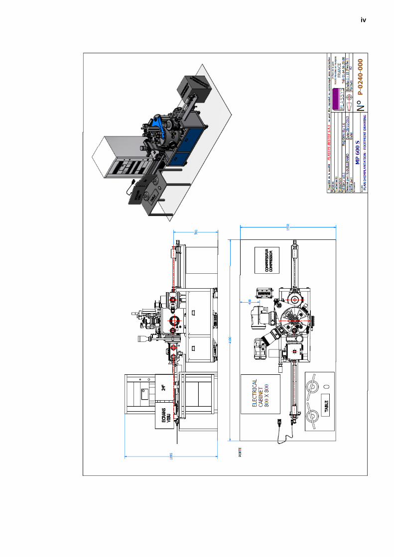
iv

v

vi
Timeline of superconducting materials grown in the sputter deposition system
Related Documents