AVR254: QWheel ® with ATtiny48 Features • Number of channels: 4 channels • Number of sensors: 1 sensor- one wheel- constituting all 4 channels • Wheel design: 4 channels • Electrode design: two-part electrode shapes (drive-receive); wide variety of possible layouts • PCB layers required: one layer (with jumpers), two layers (no jumpers) • Electrode materials: PCB, FPCB, silver or carbon on film, ITO on film • Panel materials: plastic, glass, composites, painted surfaces (low particle density metallic paints possible) • Adjacent metal: compatible with grounded metal immediately next to keys • Wheel sensitivity: individually settable via simple commands over TWI interface • Interface: Two-wire Serial Interface (Philips ® I 2 C-compatible slave mode @ 100kHz) • Moisture tolerance: best in class • Power: 1.8 V to 5.5 V • Signal processing: self-calibration • Applications: laptop, mobile, consumer appliances, PC peripherals etc. • Technology: patented spread-spectrum charge-transfer (transverse mode) • Patent & Trademarks : - QMatrix™ (patented charge-transfer method) - AKS™ (patented Adjacent Key Suppression ® ) technology - QWheel (patented charge-transfer method) 1 Overview This Application Note focuses on making a customized firmware solution using Atmel ® QTouch ® Library designed for a wheel (constructed from 4 channels). The firmware has the capabilities to configure/sense the touch on the wheel and report the changes to the Host using Atmel’s TWI (Two-wire Serial Interface) which is compatible to Philips I 2 C Interface. The firmware uses the QMatrix technology for sensing and detecting the touch on the wheel. The QMatrix technology employs transverse charge-transfer sensing electrode designs which can be made very compact and are easily wired. Charge is forced from an emitting electrode into the overlying panel dielectric, and then collected on a receiver electrode. This directs the charge into a sampling capacitor which is then converted directly to digital form, without the use of amplifiers. The channels are configured in a matrix format that minimizes the number of required scan lines and device pins. The key electrodes can be designed into a conventional Printed Circuit Board (PCB) or Flexible Printed Circuit Board (FPCB) as a copper pattern, or as printed conductive ink on plastic film. 8-bit Microcontrollers Application Note Preliminary Rev. 8262A-AVR-10/09

Welcome message from author
This document is posted to help you gain knowledge. Please leave a comment to let me know what you think about it! Share it to your friends and learn new things together.
Transcript
AVR254: QWheel® with ATtiny48
Features • Number of channels: 4 channels • Number of sensors: 1 sensor- one wheel- constituting all 4 channels • Wheel design: 4 channels • Electrode design: two-part electrode shapes (drive-receive); wide variety of
possible layouts • PCB layers required: one layer (with jumpers), two layers (no jumpers) • Electrode materials: PCB, FPCB, silver or carbon on film, ITO on film • Panel materials: plastic, glass, composites, painted surfaces (low particle density
metallic paints possible) • Adjacent metal: compatible with grounded metal immediately next to keys • Wheel sensitivity: individually settable via simple commands over TWI interface • Interface: Two-wire Serial Interface (Philips® I2C-compatible slave mode @ 100kHz) • Moisture tolerance: best in class • Power: 1.8 V to 5.5 V • Signal processing: self-calibration • Applications: laptop, mobile, consumer appliances, PC peripherals etc. • Technology: patented spread-spectrum charge-transfer (transverse mode) • Patent & Trademarks :
- QMatrix™ (patented charge-transfer method) - AKS™ (patented Adjacent Key Suppression®) technology - QWheel (patented charge-transfer method)
1 Overview This Application Note focuses on making a customized firmware solution using Atmel® QTouch® Library designed for a wheel (constructed from 4 channels). The firmware has the capabilities to configure/sense the touch on the wheel and report the changes to the Host using Atmel’s TWI (Two-wire Serial Interface) which is compatible to Philips I2C Interface. The firmware uses the QMatrix technology for sensing and detecting the touch on the wheel. The QMatrix technology employs transverse charge-transfer sensing electrode designs which can be made very compact and are easily wired. Charge is forced from an emitting electrode into the overlying panel dielectric, and then collected on a receiver electrode. This directs the charge into a sampling capacitor which is then converted directly to digital form, without the use of amplifiers.
The channels are configured in a matrix format that minimizes the number of required scan lines and device pins. The key electrodes can be designed into a conventional Printed Circuit Board (PCB) or Flexible Printed Circuit Board (FPCB) as a copper pattern, or as printed conductive ink on plastic film.
8-bit Microcontrollers Application Note Preliminary
Rev. 8262A-AVR-10/09
2 AVR254 8262A-AVR-10/09
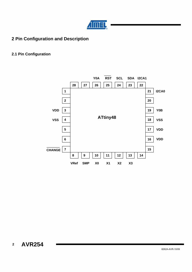
2 Pin Configuration and Description
2.1 Pin Configuration
ATtiny48
RST
28 27 26 25 24 23 22
8 9 10 11 12 13 14
21
20
19
18
17
16
15
1
2
3
4
5
6
7
SCL SDA I2CA1 Y0A
Y0B
VSS
VDD
VDD
VDD
VSS
CHANGE
VRef SMP X0 X1 X2 X3
I2CA0

AVR254
3
8262A-AVR-09/09
2.2 Pin Configuration Description
Table 2-1. Pin Listing
Pin
Function
I/O Comments If unused,
Connect To...
3 VDD P Power - 4 VSS P Supply ground - 7 _______
CHANGE OD State change notification Leave open
8 VRef P Supply ground - 9 SMP O Sample output. -
10 X0 O X matrix drive line Leave open 11 X1 O X matrix drive line Leave open 12 X2 O X matrix drive line Leave open 13 X3 O X matrix drive line Leave open 16 VDD P Power -
17 VDD P Power -
18 VSS P Supply ground - 19 Y0B I/O Y line connection Leave open
21 I2CA0 I TWI (I2C-compatible) address select
22 I2CA1 I TWI (I2C-compatible) address select
23 SDA OD Serial Interface Data - 24 SCL OD Serial Interface Clock -
25
____ RST
I Reset low; has internal 30k - 60k
pull- up Leave open or
VDD
26 Y0A I/O Y line connection Leave open

4 AVR254 8262A-AVR-10/09
3 Introduction
The customized firmware facilitates a digital burst mode charge-transfer sensor designed specifically for matrix layout touch controls; it includes all signal processing functions necessary to provide stable sensing under a wide variety of changing conditions. Only a few external parts are required for operation. The entire circuit can be built within a few square centimeters of single-sided PCB area. CEM-1 and FR1 punched, single-sided materials can be used for the lowest possible cost. The PCB’s rear can be mounted flush on the back of a glass or plastic panel using a conventional adhesive, such as 3M VHB two-sided adhesive acrylic film.
The firmware employs transverse charge-transfer sensing, a technology that senses changes in electrical charge forced across two electrode elements by a pulse edge.
The firmware uses Atmel’s TWI (Two-wire Serial Interface) which is compatible to Philips I2C interface to allow sensor data to be extracted and to permit sensor parameter setup. The command structure is designed to minimize the amount of data traffic while maximizing the amount of information conveyed.
3.1 QWheel The Tiny48 customized firmware is formed with 4 channels which are used to make a wheel. These can be located anywhere within an electrical grid of 4X and 1Y scan lines.
Additional processing can be done on the channels to form a wheel. The wheel will have to start at X0 and use only Y0. The wheel uses 4 channels.
3.2 Enabling/Disabling QWheel
Wheel can be enabled by setting a nonzero burst length for all the 4 channels.
A zero burst length for all the channels disables the wheel sensor.
AVR254
5
8262A-AVR-09/09
4 Hardware and Functional
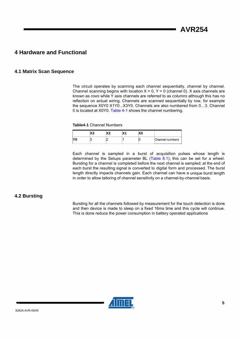
4.1 Matrix Scan Sequence
The circuit operates by scanning each channel sequentially, channel by channel. Channel scanning begins with location X = 0, Y = 0 (channel 0). X axis channels are known as rows while Y axis channels are referred to as columns although this has no reflection on actual wiring. Channels are scanned sequentially by row, for example the sequence X0Y0 X1Y0...X3Y0. Channels are also numbered from 0…3. Channel 0 is located at X0Y0. Table 4-1 shows the channel numbering.
Table4-1 Channel Numbers
X3 X2 X1 X0
Y0 3 2 1 0 Channel numbers
Each channel is sampled in a burst of acquisition pulses whose length is determined by the Setups parameter BL (Table 8.1); this can be set for a wheel. Bursting for a channel is completed before the next channel is sampled; at the end of each burst the resulting signal is converted to digital form and processed. The burst length directly impacts channels gain. Each channel can have a unique burst length in order to allow tailoring of channel sensitivity on a channel-by-channel basis.
4.2 Bursting Bursting for all the channels followed by measurement for the touch detection is done and then device is made to sleep on a fixed 16ms time and this cycle will continue. This is done reduce the power consumption in battery operated applications

6 AVR254 8262A-AVR-10/09
4.3 Cs Sample Capacitor Operation
Cs capacitor (Cs0) absorb charge from the channel electrodes on the rising edge of each X pulse. On each falling edge of X, the Y matrix line is clamped to ground to allow the electrode and wiring charges to neutralize in preparation for the next pulse. With each X pulse charge accumulates on Cs causing a staircase increase in its differential voltage.
After the burst completes, the device clamps the Y line to ground causing the opposite terminal to go negative. The charge on Cs is then measured using an external resistor to ramp the negative terminal upwards until a zero crossing is achieved. The time required to zero cross becomes the measurement result.
The value of these capacitors is not critical but 4.7nF is recommended for most cases. They should be 10 percent X7R ceramic. If the transverse capacitive coupling from X to Y is large enough the voltage on a Cs capacitor can saturate, destroying gain. In such cases the burst length should be reduced and/or the Cs value increased. See Section 4.4.
If a Y line is not used its corresponding Cs capacitor may be omitted and the pins left floating.
4.4 Sample Capacitor Saturation
Cs voltage saturation at a pin YnB is shown in Figure 4-1. Saturation begins to occur when the voltage at a YnB pin becomes more negative than -0.25V at the end of the burst. This nonlinearity is caused by excessive voltage accumulation on Cs inducing conduction in the pin protection diodes. This badly saturated signal destroys channel gain and introduces a strong thermal coefficient which can cause phantom detection. The cause of this is either from the burst length being too long, the Cs value being too small, or the X-Y transfer coupling being too large. Solutions include loosening up the key structure interleaving, more separation of the X and Y lines on the PCB, increasing Cs, and decreasing the burst length.
Increasing Cs will make the part slower; decreasing burst length will make it less sensitive. A better PCB layout and a looser key structure (up to a point) have no negative effects. Cs voltages should be observed on an oscilloscope with the matrix layer bonded to the panel material; if the Rs side of any Cs ramps more negative than -0.25 volts during any burst (not counting overshoot spikes which are probe artifacts), there is a potential saturation problem.

AVR254
7
8262A-AVR-09/09
Figure 4-2 shows a defective waveform similar to that of Figure 4-1, but in this case the distortion is caused by excessive stray capacitance coupling from the Y line to AC ground; for example, from running too near and too far alongside a ground trace, ground plane, or other traces. The excess coupling causes the charge-transfer effect to dissipate a significant portion of the received charge from a channel into the stray capacitance. This phenomenon is more subtle; it can be best detected by increasing BL to a high count and watching what the waveform does as it descends towards and below -0.25V. The waveform will appear deceptively straight, but it will slowly start to flatten even before the -0.25V level is reached.
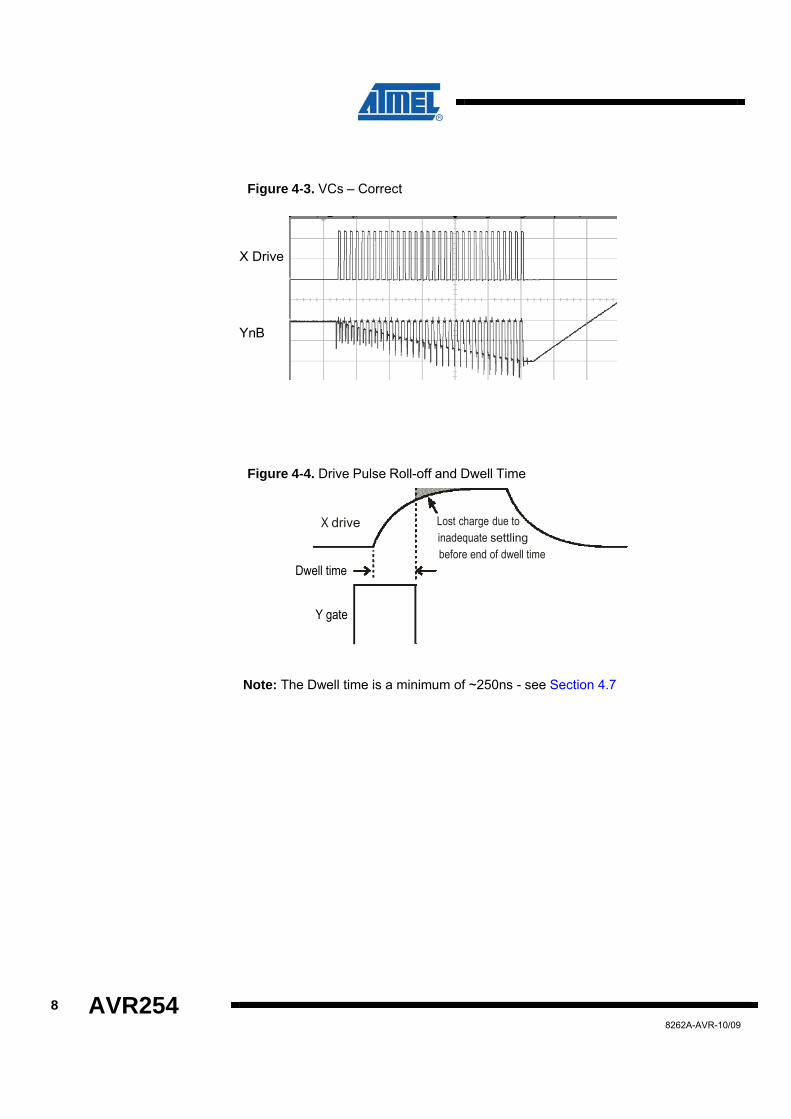
A correct waveform is shown in Figure 4-3. Note that the bottom edge of the bottom trace is substantially straight (ignoring the downward spikes).
Unlike other charge-transfer circuits, the Cs capacitor values on Tiny48 firmware have no effect on conversion gain. However, they do affect conversion time.
Unused Y lines should be left open.
Figure 4-1. VCs – Nonlinear During Burst (Burst too long, or Cs too small, or X-Y transcapacitance too large)
X Drive YnB
Figure 4-2.VCs – Poor Gain, Nonlinear During Burst (Excess capacitance from Y line to Gnd)
8 AVR254 8262A-AVR-10/09
Figure 4-3. VCs – Correct X Drive YnB
Figure 4-4. Drive Pulse Roll-off and Dwell Time X drive Lost charge due to inadequate settling before end of dwell time Dwell time
Y gate Note: The Dwell time is a minimum of ~250ns - see Section 4.7
AVR254
9
8262A-AVR-09/09
4.5 Sample Resistor The sample resistor (Rs0) is used to perform single-slope ADC conversion of the acquired charge on each Cs capacitor. These resistors directly control acquisition gain; larger values of Rs will proportionately increase signal gain. For most applications Rs should be 1MΩ.
Unused Y lines do not require an Rs resistor.
4.6 Signal Levels The signal values should normally be in the range of 200 to 750 counts with properly designed key shapes and values of Rs. However, long adjacent runs of X and Y lines can also artificially boost the signal values, and induce signal saturation; this is to be avoided. The X-to-Y coupling should come mostly from intra-key electrode coupling, not from stray X-to-Y trace coupling.
The signal swing from the smallest finger touch should preferably exceed 8 counts, with 12 being a reasonable target. The signal threshold setting (NTHR) should be set to a value guaranteed to be less than the signal swing caused by the smallest touch.
Increasing the burst length (BL) parameter will increase the signal strengths, as will increasing the sampling resistor (Rs) values.
4.7 Matrix Series Resistors The X and Y matrix scan lines can use series resistors (Rx0...Rx3 and Ry0 respectively) for improved EMC performance.
X drive lines require Rx in most cases to reduce edge rates and thus reduce RF emissions. Values range from 1kΩ to 20kΩ, typically 1kΩ.
Y lines need Ry to reduce EMC susceptibility problems and in some extreme cases, ESD. Typical Y values are about 1kΩ. Y resistors act to reduce noise susceptibility problems by forming a natural low-pass filter with the Cs capacitors.
It is essential that the Rx and Ry resistors and Cs capacitors be placed very close to the chip. Placing these parts more than a few millimeters away opens the circuit up to high frequency interference problems (above 20 MHz) as the trace lengths between the components and the chip start to act as RF antennae.
The upper limits of Rx and Ry are reached when the signal level and hence key sensitivity are clearly reduced. The limits of Rx and Ry will depend on key geometry and stray capacitance, and thus an oscilloscope is required to determine optimum values of both.

10 AVR254 8262A-AVR-10/09
Dwell time is the duration in which charge coupled from X to Y is captured as shown in Figure 4-4. Increasing Rx values will cause the leading edge of the X pulses to increasingly roll off, causing the loss of captured charge (and hence loss of signal strength) from the channels.
The dwell time is a minimum of 250 ns. If the X pulses have not settled within 250 ns, channel gain will be reduced; if this happens, either the stray capacitance on the X line(s) should be reduced (by a layout change, for example by reducing X line exposure to nearby ground planes or traces), or, the Rx resistor needs to be reduced in value (or a combination of both approaches).
One way to determine X line settling time is to monitor the fields using a patch of metal foil or a small coin over the key (Figure 4-5). Only one key along a particular X line needs to be observed, 250 ns dwell time should exceed the observed 95 percent settling of the X-pulse by 25 percent or more.
In almost all cases, Ry should be set equal to Rx, which will ensure that the charge on the Y line is fully captured into the Cs capacitor.
Figure 4-5.Probing X-Drive Waveforms with a Coin
AVR254
11
8262A-AVR-09/09
4.8 Setting the QWheel Group of channels can be configured as a wheel. The wheel uses the Y0 line of the matrix and must start at X0, with the channels placed in consecutive numerical order. The wheel constitutes of four channels on the Y0 line, with first channel starting as X0Y0, second channel X1Y0, third X2Y0 and fourth X3Y0.
Stability of the reported position will be dependent on the amount of signal on the wheel channels. Running at higher resolutions, with a thick panel might produce a fluctuating reported position.
4.9 PCB Layout, Construction
4.9.1 Overview
It is best to place the chip near the touch keys on the same PCB so as to reduce X and Y trace lengths, thereby reducing the chances for EMC problems. Long connection traces act as RF antennae. The Y (receive) lines are much more susceptible to noise pickup than the X (drive) lines. Even more importantly, all signal related discrete parts (resistors and capacitors) should be very close to the body of the chip. Wiring between the chip and the various resistors and capacitors should be as short and direct as possible to suppress noise pickup.
Ground planes, if used, should be placed under or around the chip itself and the associated resistors and capacitors in the circuit, under or around the power supply, and back to a connector. Ground planes can be used to shield against radiated noise, but at the expense of a reduction in sensitivity as described previously.
Note: When using ground planes/floods, parasitic capacitance on Y lines can lead to reduced charge- transfer efficiency. For noise suppression, ground planes/floods can be beneficial around and between keys on the touch side of the PCB. However, it is advisable to route Y lines on the PCB layer furthest away from the plane/flood, to reduce parasitic capacitance. Cross-hatched ground patterns can act as effective shields, while helping to reduce parasitic capacitance. Ground planes/floods around the chip are generally acceptable, taking into account the same considerations as for the Y line parasitics.
12 AVR254 8262A-AVR-10/09
4.9.2 LED Traces and Other Switching Signals
Digital switching signals near the Y lines will induce transients into the acquired signals, deteriorating the SNR performance of the device. Such signals should be routed away from the Y lines, or the design should be such that these lines are not switched during the course of signal acquisition (bursts).
LED terminals which are multiplexed or switched into a floating state and which are within or physically very near a key structure (even if on another nearby PCB) should be bypassed to either Vss or Vdd with at least a 10nF capacitor to suppress capacitive coupling effects which can induce false signal shifts. The bypass capacitor does not need to be next to the LED, in fact it can be quite distant. The bypass capacitor is noncritical and can be of any type.
LED terminals which are constantly connected to Vss or Vdd do not need further bypassing.
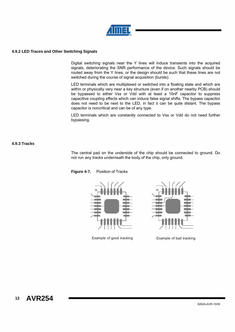
4.9.3 Tracks
The central pad on the underside of the chip should be connected to ground. Do not run any tracks underneath the body of the chip, only ground.
Figure 4-7. Position of Tracks
Example of good tracking Example of bad tracking

AVR254
13
8262A-AVR-09/09
4.9.4 PCB Cleanliness
All capacitive sensors should be treated as highly sensitive circuits which can be influenced by stray conductive leakage paths. Charge-transfer devices have a basic resolution in the femtofarad range; in this region, there is no such thing as “clean flux". Flux absorbs moisture and becomes conductive between solder joints, causing signal drift and resultant false detections or transient losses of sensitivity or instability. Conformal coatings will trap in existing amounts of moisture which will then become highly temperature sensitive.
The designer should specify ultrasonic cleaning as part of the manufacturing process, and in cases where a high level of humidity is anticipated, the use of conformal coatings after cleaning to keep out moisture.
4.10 Power Supply Considerations
See Section 10.2 for the Vdd range and short-term power supply fluctuations. If the power supply fluctuates slowly with temperature, the device will track and compensate for these changes automatically with only minor changes in sensitivity. If the supply voltage drifts or shifts quickly, the drift compensation mechanism will not be able to keep up, causing sensitivity anomalies or false detections.
As the device uses the power supply itself as an analog reference, the power should be very clean and come from a separate regulator. A standard inexpensive Low Dropout (LDO) type regulator should be used that is not also used to power other loads such as LEDs, relays, or other high current devices. Load shifts on the output of the LDO can cause Vdd to fluctuate enough to cause false detection or sensitivity shifts.
Caution: A regulator IC shared with other logic devices can result in erratic operation and is not advised.
A regulator can be shared among two or more charge-transfer devices on one board. A single ceramic 0.1uF bypass capacitor, with short traces, should be placed very close to supply pins 3 and 4 of the IC. Failure to do so can result in device oscillation, high current consumption, erratic operation etc. Pins 16 and 17 do not require bypassing if the traces between these pins and power traces are short.
4.11 Startup/Calibration Times
The device requires initialization times of approximately 70ms. The CHANGE will go low and calibration will start (takes 15 matrix scans), after this start up period is over.
14 AVR254 8262A-AVR-10/09
4.12 Calibration
Calibration does not happen periodically. The Wheel is only calibrated on power-up and when:
• Enabled
AND
– the signal delta value is greater than the positive threshold value, defined as
reference value plus three-quarters of the negative threshold.
OR
– the user issues a recalibrate command.
An interrupt on CHANGE pin occurs when there is a change in the wheel status bytes. An interrupt will occur on calibration only if at least one of the wheel was in detect as recalibration will then cause a status change.
4.13 Reset Input
The RST pin can be used to reset the device to simulate a power-down cycle, in order to bring the device up into a known state should communications with the device be lost. The pin is active low, and a low pulse lasting at least 10µs must be applied to this pin to cause a reset. If an external hardware reset is not used, the reset pin may be connected to Vdd.
4.14 Detection Integrator
The device features a detection integration mechanism, which acts to confirm a detection in a robust fashion. A per-key counter is incremented each time the key has exceeded its threshold and stayed there for a number of acquisitions. When this counter reaches a preset limit the key is finally declared to be touched.
For example, if the limit value is 10, then the device has to exceed its threshold and stay there for 10 acquisitions in succession without going below the threshold level, before the key is declared to be touched. If on any acquisition the signal is not seen to exceed the threshold level, the counter is cleared and the process has to start from the beginning.
AVR254
15
8262A-AVR-09/09
4.15 Sleep
The device performs a set of measurements and then sleep for 16ms (default value) to conserve power, and this cycle keeps on repeating unless LP Mode is changed to some other value.
There are two user-configurable sleep modes; Low Power (LP) mode and SLEEP mode. The LP setting is used for conserving power as shown in Section7.9. This will determine how often the device wakes up to do drift compensation. It also determines the maximum response time to the first touch after inactivity.
When a valid touch is registered, the device enters default sleep time (16ms) for a faster response to wheel touch. The device will stay in this mode if it continues to see wheel being touched and released. A low power setting of zero causes the device to enter an ultra-low power mode (SLEEP), where no measurements are carried out. SLEEP mode also stops the internal watchdog timer, so that the part is totally dormant, and current drain is <.3µA.
The Tiny48 customized firmware wakes from SLEEP mode if there is address match on the TWI-bus, reset on the RST pin or an LP mode is set.
16 AVR254 8262A-AVR-10/09
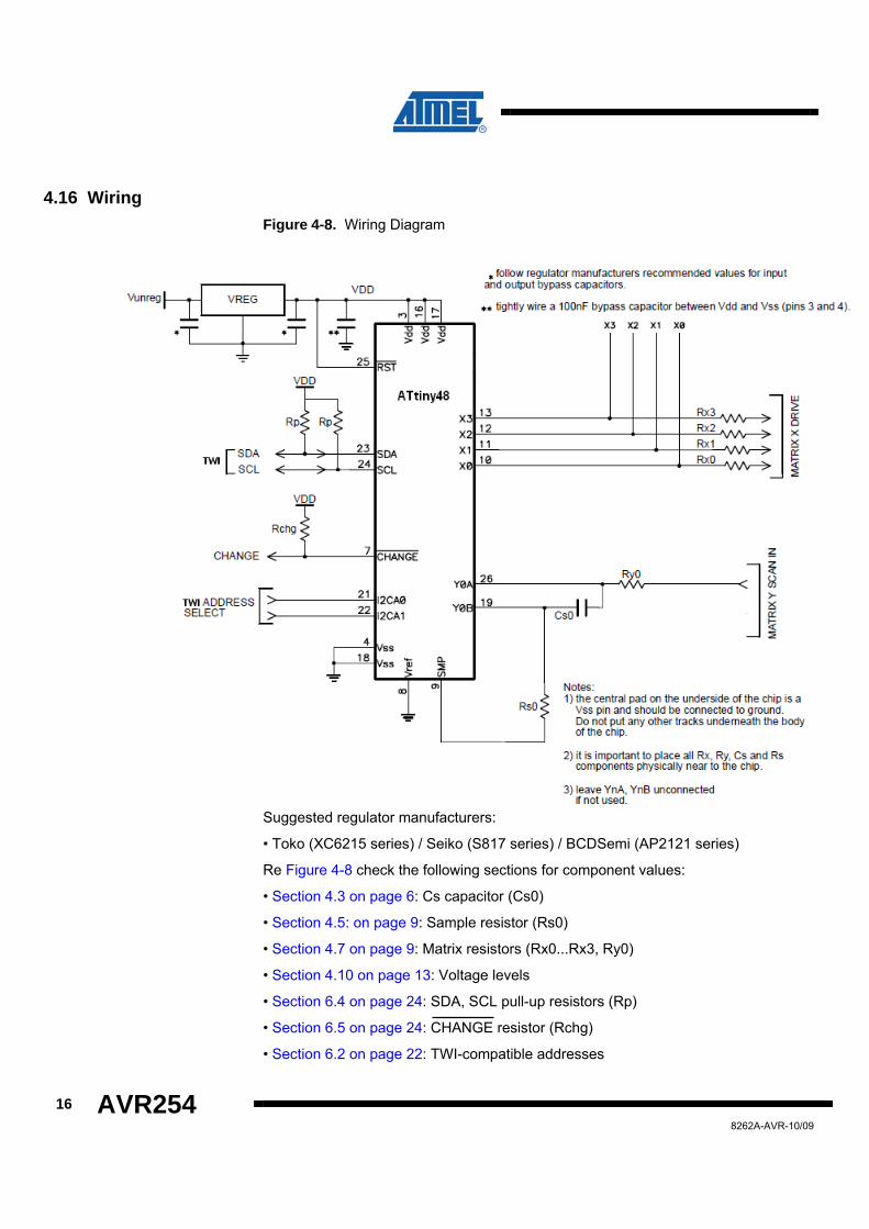
4.16 Wiring Figure 4-8. Wiring Diagram
Suggested regulator manufacturers:
• Toko (XC6215 series) / Seiko (S817 series) / BCDSemi (AP2121 series)
Re Figure 4-8 check the following sections for component values:
• Section 4.3 on page 6: Cs capacitor (Cs0)
• Section 4.5: on page 9: Sample resistor (Rs0)
• Section 4.7 on page 9: Matrix resistors (Rx0...Rx3, Ry0)
• Section 4.10 on page 13: Voltage levels
• Section 6.4 on page 24: SDA, SCL pull-up resistors (Rp)
• Section 6.5 on page 24: CHANGE resistor (Rchg)
• Section 6.2 on page 22: TWI-compatible addresses
AVR254
17
8262A-AVR-09/09
5 TWI (Two-wire Serial Interface) Bus Operation
5.1 Interface Bus
More detailed information about Atmel’s TWI (Two-wire Serial Interface) which is compatible with Philips I2C Bus/Protocol, is available on Atmel’s official website: http://www.atmel.com/dyn/resources/prod_documents/doc2565.pdf
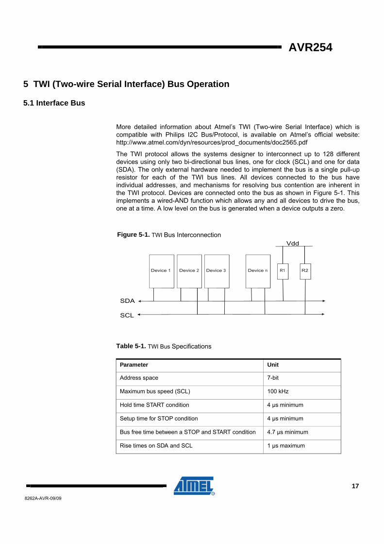
The TWI protocol allows the systems designer to interconnect up to 128 different devices using only two bi-directional bus lines, one for clock (SCL) and one for data (SDA). The only external hardware needed to implement the bus is a single pull-up resistor for each of the TWI bus lines. All devices connected to the bus have individual addresses, and mechanisms for resolving bus contention are inherent in the TWI protocol. Devices are connected onto the bus as shown in Figure 5-1. This implements a wired-AND function which allows any and all devices to drive the bus, one at a time. A low level on the bus is generated when a device outputs a zero.
Vdd
Device 1 Device 2 Device 3 Device n R1 R2
SDA
SCL
Table 5-1. TWI Bus Specifications
Parameter Unit
Address space 7-bit
Maximum bus speed (SCL) 100 kHz
Hold time START condition 4 µs minimum
Setup time for STOP condition 4 µs minimum
Bus free time between a STOP and START condition 4.7 µs minimum
Rise times on SDA and SCL 1 µs maximum
Figure 5-1. TWI Bus Interconnection
18 AVR254 8262A-AVR-10/09
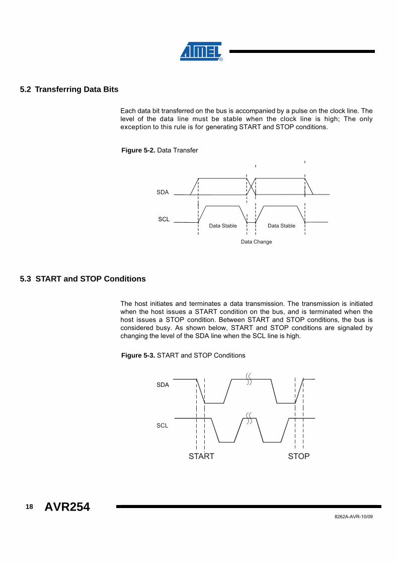
5.2 Transferring Data Bits
Each data bit transferred on the bus is accompanied by a pulse on the clock line. The level of the data line must be stable when the clock line is high; The only exception to this rule is for generating START and STOP conditions.
SDA
SCL Data Stable Data Stable
Data Change
5.3 START and STOP Conditions
The host initiates and terminates a data transmission. The transmission is initiated when the host issues a START condition on the bus, and is terminated when the host issues a STOP condition. Between START and STOP conditions, the bus is considered busy. As shown below, START and STOP conditions are signaled by changing the level of the SDA line when the SCL line is high.
SDA
SCL
START STOP
Figure 5-2. Data Transfer
Figure 5-3. START and STOP Conditions
AVR254
19
8262A-AVR-09/09
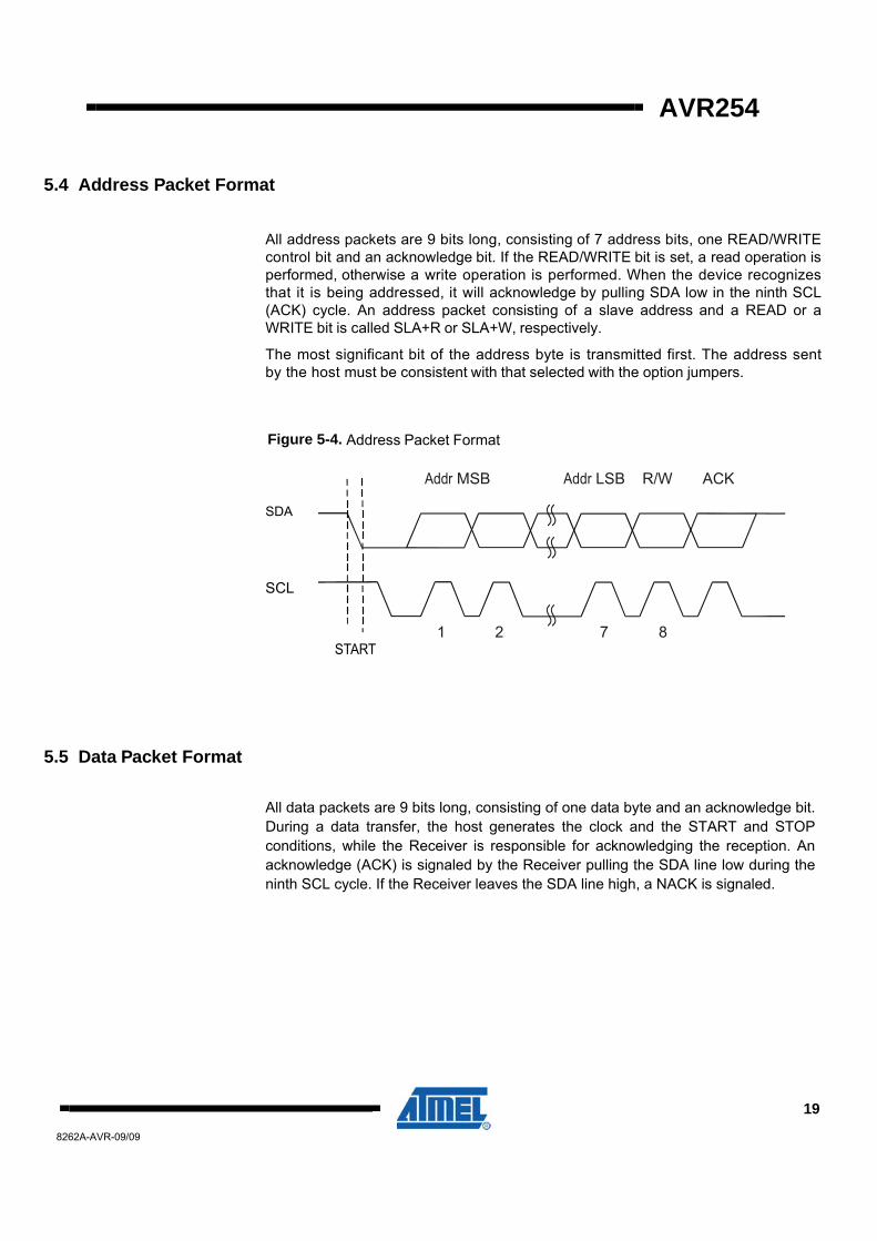
5.4 Address Packet Format
All address packets are 9 bits long, consisting of 7 address bits, one READ/WRITE control bit and an acknowledge bit. If the READ/WRITE bit is set, a read operation is performed, otherwise a write operation is performed. When the device recognizes that it is being addressed, it will acknowledge by pulling SDA low in the ninth SCL (ACK) cycle. An address packet consisting of a slave address and a READ or a WRITE bit is called SLA+R or SLA+W, respectively.
The most significant bit of the address byte is transmitted first. The address sent by the host must be consistent with that selected with the option jumpers.
Addr MSB Addr LSB R/W ACK SDA
SCL
1 2 7 8 START
5.5 Data Packet Format All data packets are 9 bits long, consisting of one data byte and an acknowledge bit. During a data transfer, the host generates the clock and the START and STOP conditions, while the Receiver is responsible for acknowledging the reception. An acknowledge (ACK) is signaled by the Receiver pulling the SDA line low during the ninth SCL cycle. If the Receiver leaves the SDA line high, a NACK is signaled.
Figure 5-4. Address Packet Format
20 AVR254 8262A-AVR-10/09
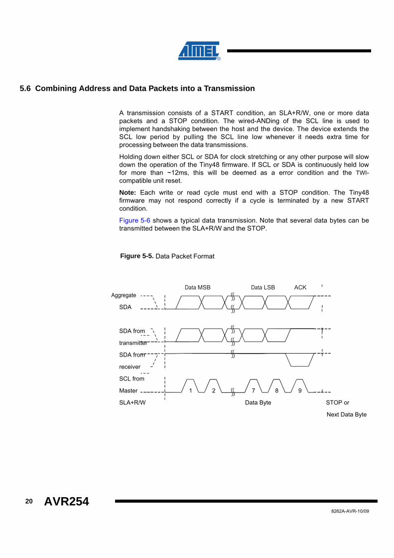
5.6 Combining Address and Data Packets into a Transmission
A transmission consists of a START condition, an SLA+R/W, one or more data packets and a STOP condition. The wired-ANDing of the SCL line is used to implement handshaking between the host and the device. The device extends the SCL low period by pulling the SCL line low whenever it needs extra time for processing between the data transmissions.
Holding down either SCL or SDA for clock stretching or any other purpose will slow down the operation of the Tiny48 firmware. If SCL or SDA is continuously held low for more than ~12ms, this will be deemed as a error condition and the TWI-compatible unit reset.
Note: Each write or read cycle must end with a STOP condition. The Tiny48 firmware may not respond correctly if a cycle is terminated by a new START condition.
Figure 5-6 shows a typical data transmission. Note that several data bytes can be transmitted between the SLA+R/W and the STOP.
Data MSB Data LSB ACK Aggregate
SDA
SDA from
transmitter
SDA from
receiver
SCL from
Master 1 2 7 8 9
SLA+R/W Data Byte STOP or
Next Data Byte
Figure 5-5. Data Packet Format

AVR254
21
8262A-AVR-09/09
Addr MSB Addr LSB R/W ACK Data MSB Data LSB ACK
SDA
SCL
1 2 7 8 9 1 2 7 8 9
START SLA+R/W Data Byte STOP
Figure 5-6. Packet Transmission
22 AVR254 8262A-AVR-10/09
6 Interfaces
6.1 TWI (Two-wire Interface) Protocol
The TWI (Two-wire Interface) protocol is based around access to an address table and supports multi-byte reads and writes.
Note: Each write or read cycle must end with a stop condition. The Tiny48 firmware may not respond correctly if a cycle is terminated by a new start condition.
6.2 TWI-Compatible Addresses
Four preset TWI (I2C-compatible) addresses are selectable through pin I2CA0 and I2CA1 (Table 6-1).
Table 6-1. TWI-Compatible Addresses
6.3 Data Read/Write
6.3.1 Writing Data to the Device
The sequence of events required to write data to the device is shown next.
Host to Device Device to Host
I2CA1 I2CA0 Address 0 0 0x0D
0 1 0X17
1 0 0X44
1 1 0X6B
S SLA+W A MemAddress A Data A P
AVR254
23
8262A-AVR-09/09
Table 5-1. Data Read/Write
The host initiates the transfer by sending the START condition, and follows this by sending the slave address of the device together with the Write-bit. The device sends an ACK. The host then sends the memory address within the device it wishes to write to. The device sends an ACK.
The host transmits one or more data bytes; each will be acknowledged by the device.
If the host sends more than one data byte, they will be written to consecutive memory addresses. The device automatically increments the target memory address after writing each data byte. After writing the last data byte, the host should send the STOP condition.
The host should not try to write beyond address 255 because the device will not increment the internal memory address beyond this.
6.3.2 Reading Data from the Device
The sequence of events required to read data from the device is shown next.
Host to Device Device to Host
S SLA+W A MemAddress A P S SLA+R A
The host initiates the transfer by sending the START condition, and follows this by sending the slave address of the device together with the Write-bit. The device sends an ACK. The host then sends the memory address within the device it wishes to read from. The device sends an ACK.
The host must then send a STOP and a START condition followed by the slave address again but this time accompanied by the Read-bit. The device will return an ACK, followed by a data byte. The host must return either an ACK or NACK. If the host returns an ACK, the device will subsequently transmit the data byte from the next address. Each time a data byte is transmitted, the device automatically increments the internal address. The device will continue to return data bytes until the host responds with a NACK. The host should terminate the transfer by issuing the
STOP condition.
Key S Start Condition
SLA+W Slave Address plus write bit
A Acknowledge bit
MemAddress Target Memory address within device
Data Data to be written
P STOP Condition
Data 1 A Data 2 A Data n /A P
24 AVR254 8262A-AVR-10/09
6.4 SDA and SCL
The TWI (I2C-compatible) bus transmits data and clock with SDA and SCL. They are open-drain; that is TWI master and slave devices can only drive these lines low or leave them open.
The Termination resistors (Rp) pull the line up to Vdd if no TWI (I2C-compatible) device is pulling it down.
The termination resistors commonly range from 1kΩ to 10kΩ and should be chosen so that the rise times on SDA and SCL meet the TWI specifications (1µs maximum).
6.5 CHANGE Pin
The CHANGE pin is an active low open drain output that can be used to alert the host of any changes to any of the 4 status bytes (address 2 to 5), thus reducing the need for wasteful TWI-compatible communications. After setting the Tiny48 firmware, host can not communicate with the device, except when CHANGE pin goes active.
CHANGE goes inactive again only when the host performs a read from all status bytes which have changed.
Poll rate: The host can make use of CHANGE pin output to initiate a communication; this will guarantee the optimal polling rate.
If the host cannot make use of CHANGE pin the poll rate should be no faster than once per matrix scan (see Section 10.4). Anything faster will not provide new information and will slow down the chip operation.
The CHANGE pin requires a pull-up resistor, with a typical value of ~100kΩ.
AVR254
25
8262A-AVR-09/09
7 Communication Protocol
7.1 Introduction
The device is address mapped. All communications consist of writes to, and reads from, locations in an 8-bit address map. Table 7-1 shows the address map of Tiny48 Customized firmware.
Table 7-1. Memory Map
Address Use Access
0 Chip ID Read
1 Major/minor code version Read
2 General Status Read
3 Wheel Touch Status Read
4-5 Wheel Touch Position Read
6 Calibrate Read/Write
7 Reset Read/Write
8 LP Mode Read/Write
9 Detect Integrity (DI) Read/Write
10 Negative threshold Read/Write
11...14 Burst Length for channels 0….3 Read/Write
15...22 Channel 0 -3 Signals Read
23...30 Channel 0 – 3 References Read
31...32 Wheel Delta Read

26 AVR254 8262A-AVR-10/09
7.2 Address 0: Chip ID
Table 7-2. Chip ID
Address b7 B6 b5 b4 b3 b2 b1 b0
0 Chip ID
There is an 8-bit chip ID, which is set at 0x0B.
7.3 Address 1: Code Version
Table 7-3. Code Version
Address b7 b6 b5 b4 b3 b2 b1 b0
1 Major Version
Minor Version
There is an 8-bit major and minor version of firmware code revision. The top nibble of the firmware version register contains the major version (e.g. 1.0) and the bottom nibble contains the minor version (e.g. 0.7).The Current Firmware Version will be 1.7 .So, when reading the version number , the value would be 0x17 which signifies the version number as 1.7
7.4 Address 2: General Status
Table 7-4. General Status
These bits indicate the general status of the device. A change in this byte will cause the CHANGE line to trigger. RESET: this bit is set after a reset. This bit is clear after this byte is read back by the host.
Address b7 b6 b5 b4 b3 b2 b1 b0
2
RESET
0
0
0
0
0
0
0
AVR254
27
8262A-AVR-09/09
7.5 Address 3: Wheel Touch Status Table 7-5. Wheel Touch Status
Address b7 b6 b5 b4 b3 b2 b1 b0
3 Touch Status( 0 or 1)
Address 3: detect touch status for wheel. This Address location indicates wheel in detection, if any, touched wheel report as “1”, untouched or disabled wheel report as “0”. A change in this byte will cause the CHANGE line to trigger.
7.6 Address 4…5: Wheel Touch Position Table 7-6. Wheel Touch Position
Address Value 4 Position
Position: Last position of the touch on the wheel.
A change in this byte will cause the CHANGE line to trigger.
7.7 Address 6: Calibrate
Table 7-7. Calibrate
Address b7 b6 b5 b4 b3 b2 b1 b0
6 CALIBRATE
Writing any nonzero value into this address will trigger the TINY48 firmware to start a recalibration on the wheel.
28 AVR254 8262A-AVR-10/09
7.8 Address 7: Reset Table 7-8. Reset
Address b7 b6 b5 b4 b3 b2 b1 b0 7 RESET
Writing value 1 will trigger the device to reset. After a reset, the device will revert to default settings. After receiving a reset command, TINY48 firmware will start not acknowledging TWI (I2C-compatible) communications and make CHANGE inactive within 16ms. The chip will reset after another ~16ms.
7.9 Address 8: LP Mode Table 7-9. LP Mode
Address b7 B6 b5 b4 b3 b2 b1 b0 8 LP_MODE
LP mode sets the sleep time between bursts. A higher value causes more sleep time between acquisitions resulting in lower power consumption, but slower response time. The values are between 0...7, with each incrementing the sleep time by certain value which are given below. For example, 1 = 16ms LP, 2 = 32ms LP, 3 = 64ms LP, 4 = 125ms LP,5 = 250 ms LP, 6 = 500 ms LP , 7 = 1000 ms LP etc. A value of zero causes the device to enter an ultra-low power mode (SLEEP), where no measurements are carried out. As the TINY48 customized firmware uses the watchdog timer to wake up from sleep , so the sleep timings are determined by the Watchdog Timeout Period available for tiny48 device based on the Watchdog Timer Prescalar values.The TINY48 firmware is designed to sleep as much as possible to conserve power. Note: The longer the LP mode, the longer the response time at first touch. The response time for the first touch includes the digital filter's settling time (a few measurement cycles) and the DI process. Above 256ms LP mode the power consumption does not reduce as much, even with longer LP mode durations. Refer to Table 10-1 for typical power consumptions. Default value: 1(16ms LP)

AVR254
29
8262A-AVR-09/09
7.10 Address 9: Detect Integrator Table 7-10. Detect Integrator
Address b7 b6 b5 b4 b3 b2 b1 b0 9 0 0 0 NDIL
NDIL is used to provide signal filtering.
To suppress false detections caused by spurious events like electrical noise, the device incorporates a 'detection integrator' or DI counter mechanism. A per-sensor counter is incremented each time the sensor has exceeded its threshold and stayed there for a number of acquisitions in succession, without going below the threshold level. When this counter reaches a preset limit the sensor is finally declared to be touched.
If on any acquisition the signal is not seen to exceed the threshold level, the counter is cleared and the process has to start from the beginning.
The TINY48 firmware has a built in minimum of 1 DI counts in addition to the NDIL value. Therefore, if setting a NDIL value of 3, the actual number of consecutive acquisitions is 4.
Available NDIL values are from 1 to 31. Default Value: 3 (4 DI value)
7.11 Address 10: Negative Threshold Table 7-11. Negative Threshold
Address b7 B6 b5 b4 b3 b2 b1 b0
10 THRESHOLD
The negative threshold value is established relative to a channel’s signal reference value. The threshold is used to determine sensor touch when crossed by a negative-going signal swing after having been filtered by the detection integrator. Larger absolute values of threshold desensitize sensor since the signal must travel farther in order to cross the threshold level. Conversely, lower thresholds make sensor more sensitive. As Cx and Cs drift, the reference point drift-compensates for these changes at a user-settable rate; the threshold level is recomputed whenever the reference point moves, and thus it also is drift compensated.
30 AVR254 8262A-AVR-10/09
The amount of NTHR required depends on the amount of signal swing that occurs when a sensor is touched. Thicker panels or smaller channel geometries reduce “channel gain", i.e. signal swing from touch, thus requiring smaller NTHR values to detect touch. Negative hysteresis: this is fixed at two less than the negative threshold value and cannot be altered. It is implemented to stop keys from dithering in and out of detect. NTHR Typical values: 5 to 12 NTHR Default value: 10 (10 counts of threshold)
7.12 Address 11..14: Burst Length Table 7-12. Burst Length
Address b7 B6 b5 b4 b3 b2 b1 b0
11…14 BURST LENGTH
The TINY48 firmware uses a fixed number of pulses which are executed in burst mode. This number is set in groups of four. Therefore, the value send to the TINY48 firmware is multiplied by four to get the actual number of burst pulses. The burst length is the number of times the charge-transfer process is performed on a given channel. Each charge-transfer process is simply the pulsing of an X line once, with a corresponding Y line enabled to capture the resulting charge passed through the channel’s capacitance Cx.
Increasing burst length directly affects channel sensitivity. This occurs because the accumulation of charge in the charge integrator is directly linked to the burst length. The burst length of each channel cannot be set individually, but it can be set for a wheel sensor as a whole which in turn will set the same burst length for all the channels used by the wheel sensor( In this case wheel constitutes of four channels ).
Apparent touch sensitivity is also controlled by the Negative Threshold level (NTHR). Burst length and NTHR interact; normally burst lengths should be kept as short as possible to reduce scan time and limit RF emissions, but NTHR should be kept above 6 to reduce false detections due to external noise. The detection integrator mechanism also helps to prevent false detections. The user can set the burst length of each channel which constitutes the wheel starting from memory map address 11 to 14. Channel 0 burst length is mapped to address 11, channel 1 to 12, channel 3 to 13 and channel 4 to 14.
Typical values: 8 to 32 (32 to 128 burst pulses) Default: 16 (64 burst pulses)

AVR254
31
8262A-AVR-09/09
7.13 Address 15….30: Signals and References Addresses 15...22 allow signal data to be read for each channel. There are two bytes of data for each channel. These are the channels’s 16-bit signal which is accessed as two 8-bit bytes, stored LSB first .As we have four channel for the wheel, so eight addresses are mapped corresponding to the signal value.
Addresses 23...30 allow reference data to be read for each channel. There are two bytes of data for each channel. These are the channel’s 16-bit reference which is accessed as two 8-bit bytes, stored LSB first. As we have four channel for the wheel, so eight addresses are mapped corresponding to the reference value.
There are a total of 4 channels and 4 bytes of data per channel, yielding a total of 16 addresses. These addresses are read-only.
Table 7-13. Signal and References
Address Channel # Use Address Channel # Use
15 0 Signal LSB 23 0 Reference LSB
16 0 Signal MSB 24 0 Reference MSB
17…22 1...3 Signal on Channel 1 to 3
25…30 1…3 Reference on Channel 1 to 3
7.14 Address 31...32: Deltas Addresses 31...32 allow delta data to be read for wheel. There are two bytes of data for wheel delta. These are the channel’s 16-bit (reference – signal) value which is accessed as two 8-bit bytes, stored LSB first. In the firmware, the delta’s for all the channels is calculated and then after arithmetic operations on that, gives the delta for the wheel.
Table 7-14. Signal Delta
Address Wheel # Use 31…32 0 Delta Value

32 AVR254 8262A-AVR-10/09
8 Setups Block
Setups data is sent from the host to the TINY48 customized firmware using the TWI (I2C-compatible) interface. The setups block is memory mapped onto this interface. Thus each setup can be accessed by reading/writing the appropriate address. Setups can be accessed individually or as a block.
Table 8-1. Setups Table
The burst length at address from 11 to 14 is for each channel from 0 to 3 which constitutes a wheel.
8.1 EEPROM Interface The TINY48 customized firmware during initialization time reads the particular location in EEPROM (Address 0x0A) .If the value at that address is found to be not equal to 0xff, it will read the Set-Up Values from the EEPROM. The configuration values are updated or written to the EEPROM when there would be a change in the configuration/setup values. The firmware will check for it and will write to the EEPROM the Updated Values during the next measurement of the touch.
Whenever the reset command comes from the host, the device get reset and it will read the configuration values from the EEPROM and update the memory map address registers with the EEPROM values.
Address
Bytes
Parameter
Symbol
Valid Range Bits
Default Value
Description
8 1
LP Mode
LP_MODE
0 – 7
8
1
0: SLEEP mode (no capacitive sensing) 1- 7: Low Power
mode
9
1
Detect Integrator
DI
1 – 31
8
4
10 1 Negative threshold
NTHR 7...12 8 10
11…14
4
Burst Length
BL
0...32
32
16 (64 pulses)
Wheel disabled if BL=0 for all channels 1...32: Burst length = BL x 4
AVR254
33
8262A-AVR-09/09
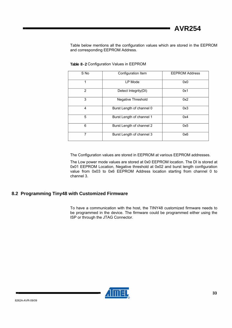
Table below mentions all the configuration values which are stored in the EEPROM and corresponding EEPROM Address.
Table 8 - 2 Configuration Values in EEPROM
S No Configuration Item EEPROM Address
1 LP Mode 0x0
2 Detect Integrity(DI) 0x1
3 Negative Threshold 0x2
4 Burst Length of channel 0 0x3
5 Burst Length of channel 1 0x4
6 Burst Length of channel 2 0x5
7 Burst Length of channel 3 0x6
The Configuration values are stored in EEPROM at various EEPROM addresses.
The Low power mode values are stored at 0x0 EEPROM location. The DI is stored at 0x01 EEPROM Location, Negative threshold at 0x02 and burst length configuration value from 0x03 to 0x6 EEPROM Address location starting from channel 0 to channel 3.
8.2 Programming Tiny48 with Customized Firmware
To have a communication with the host, the TINY48 customized firmware needs to be programmed in the device. The firmware could be programmed either using the ISP or through the JTAG Connector.

34 AVR254 8262A-AVR-10/09
9 Getting Started with TINY48 Customized Firmware
9.1 Using TWI (I2C-compatible) Bus The TINY48 customized firmware is an address-mapped part. All commands and data transfers consist of reads from, and writes to, memory location.
9.2 Establishing Contact To establish that the device is present and running, write a zero to it (see Section 9.3). Now read a single byte (see Section 9.4). This byte should be the ID of the device firmware (0x0B). If this is the case the device is present and running.
9.3 Writing to the Device A write cycle to the device consists of a start condition followed by the TWI (I2C-compatible) address of the device (see Section 6.1). The next byte is the address of the location into which the writing will start. This address is then stored as the address pointer.
Subsequent bytes in a multi-byte transfer will be written to the location of the address pointer, location of the address pointer +1, location of the address pointer +2 etc. This ends with the stop condition on the TWI (I2C-compatible) bus. A new write cycle will involve sending another address pointer.
It is possible to stop the write after the address pointer is sent if no data is required to be written to the device. This is done when setting the address pointer for reading data.
9.4 Reading from the Device A read cycle consists of a start condition followed by the TWI (I2C-compatible) address of the device (see Section 6.1). Bytes can then be read starting at the location pointed to by the address pointer set by the last write operation. The address is internally incremented for each byte read during a multi-byte read.
The stop condition at the end of the transfer causes the internal address pointer to revert to the value written during the last write operation. This means that if a set of data bytes needs to be read many times (such as the status bytes) then it is not necessary to keep sending an address pointer. It can be set to the first location and multi-byte reads will always then start there.
AVR254
35
8262A-AVR-09/09
9.5 Wheel A group of 4 channels on the Y0 line acts as a wheel. These have to be placed in numerical order starting with X0 and with no missing channels in the sequence. The number of channel needed in a Wheel is fixed as 4.
Now as the wheel is enabled, touching it will result in a wheel position being reported in the Wheel Touch Position byte.
If the wheel position is noisy, try reducing the panel thickness or increasing the sensitivities of the channels/forming the wheel, to get more signal for positional/Angle calculations.
9.6 Typical Initialization and Usage Figure 9-1 shows a typical example of communicating with the TINY48 firmware. 1. After a reset/power-up, wait for CHANGE to go low, indicating the TINY48 firmware has initialized and is ready to communicate. 2. Send all the setup parameters that need to be changed from the startup default values. 3 . After setting up the TINY48 firmware, send a Calibrate command. 4. Read all status bytes once (address 2 to 5), to return the CHANGE line to an inactive state. 5. If CHANGE line goes low, perform a read of the required status byte. All the status
bytes that have changed need to be read, to ensure that the CHANGE line goes
inactive again.
6. Process the received byte accordingly. 7. Check the reset bit in the general status byte (address 2). If it is a 1, go to step 2 to resend all the setup parameters, as a reset has occurred. If it is a 0, proceed to the next step. 8. Repeat steps 5, 6 and 7. Steps 5 and 6 are the continuous normal operating loop
sequence after initialization.

36 AVR254 8262A-AVR-10/09
Figure 9-1 Initialization Sequence
Yes
No
Yes
No
Reset/Power Up
__________Change
Pin active low No
Send Set Up Parameter to set Tiny48
__________Change
Pin active low
Read status bytes (Address 2…5 to restore change pin to inactive (high)
Send Calibrate Command
Yes
Read required status bytes and other status bytes to restore change pin to inactive (high)
Host Process receive status bytes
Reset occured
AVR254
37
8262A-AVR-09/09
10 Specifications
10.1 Absolute Maximum Specifications
10.2 Recommended Operating Conditions
Operating temp -40oC to +85oCStorage temp -55oC to +125oC Vdd +1.8V to 5.5V Supply ripple + noise* (<1MHz) ±25 mV Supply ripple + noise* (>1MHz) ±50 mV Cx transverse load capacitance per key 2 to 20 pF
VDD -0.5 to +6V
Max continuous pin current, any control or drive pin
±10 mA
Short circuit duration to ground, any pin Infinite
Short circuit duration to Vdd, any pin Infinite
Voltage forced onto any pin -0.6V to (Vdd + 0.6) Volts
CAUTION: Stresses beyond those listed under “Absolute Maximum Specifications" may cause permanent damage to the device. This is a stress rating only and functional operation of the device at these or other conditions beyond those indicated in theoperational sections of this specification is not implied. Exposure to absolutemaximum specification conditions for extended periods may affect device reliability.

38 AVR254 8262A-AVR-10/09
10.3 Power Consumption
Table 10-1. Average Current Consumption Test condition: 4 Channel Wheel Enabled, BL = 16 (4 x 16 = 64 actual pulses)
10.4 Revision History
Idd (µA) Vdd= 3.3V
LP Mode
3.3V
SLEEP <0.3
LP 16 ms 363
LP 32 ms 200
LP 64 ms 107
LP 128 ms 59
LP 256 ms 32
LP 512 ms 19
LP 1024 ms 12
Revision No. History
Firmware Revision 1.7 – July 2009
• Initial Release

8262A-AVR-09/09
Disclaimer Headquarters International
Atmel Corporation 2325 Orchard Parkway San Jose, CA 95131 USA Tel: 1(408) 441-0311 Fax: 1(408) 487-2600
Atmel Asia Unit 1-5 & 16, 19/F BEA Tower, Millennium City 5418 Kwun Tong Road Kwun Tong, Kowloon Hong Kong Tel: (852) 2245-6100 Fax: (852) 2722-1369
Product Contact
Atmel Europe Le Krebs 8, Rue Jean-Pierre Timbaud BP 309 78054 Saint-Quentin-en-Yvelines Cedex France Tel: (33) 1-30-60-70-00 Fax: (33) 1-30-60-71-11
Atmel Japan 9F, Tonetsu Shinkawa Bldg. 1-24-8 Shinkawa Chuo-ku, Tokyo 104-0033 Japan Tel: (81) 3-3523-3551 Fax: (81) 3-3523-7581
Web Site www.atmel.com
Technical Support [email protected]
Sales Contact www.atmel.com/contacts
Literature Request www.atmel.com/literature
Disclaimer: The information in this document is provided in connection with Atmel products. No license, express or implied, by estoppel or otherwise, to any intellectual property right is granted by this document or in connection with the sale of Atmel products. EXCEPT AS SET FORTH IN ATMEL’S TERMS AND CONDITIONS OF SALE LOCATED ON ATMEL’S WEB SITE, ATMEL ASSUMES NO LIABILITY WHATSOEVER AND DISCLAIMS ANY EXPRESS, IMPLIED OR STATUTORY WARRANTY RELATING TO ITS PRODUCTS INCLUDING, BUT NOT LIMITED TO, THE IMPLIED WARRANTY OF MERCHANTABILITY, FITNESS FOR A PARTICULAR PURPOSE, OR NON-INFRINGEMENT. IN NO EVENT SHALL ATMEL BE LIABLE FOR ANY DIRECT, INDIRECT, CONSEQUENTIAL, PUNITIVE, SPECIAL OR INCIDENTAL DAMAGES (INCLUDING, WITHOUT LIMITATION, DAMAGES FOR LOSS OF PROFITS, BUSINESS INTERRUPTION, OR LOSS OF INFORMATION) ARISING OUT OF THE USE OR INABILITY TO USE THIS DOCUMENT, EVEN IF ATMEL HAS BEEN ADVISED OF THE POSSIBILITY OF SUCH DAMAGES. Atmel makes no representations or warranties with respect to the accuracy or completeness of the contents of this document and reserves the right to make changes to specifications and product descriptions at any time without notice. Atmel does not make any commitment to update the information contained herein. Unless specifically provided otherwise, Atmel products are not suitable for, and shall not be used in, automotive applications. Atmel’s products are not intended, authorized, or warranted for use as components in applications intended to support or sustain life. © 2009 Atmel Corporation. All rights reserved. Atmel®, Atmel logo and combinations thereof, AVR®, AVR® logo, QWheel®, QTouch®, Adjacent Key Suppression® and others, are the registered trademarks, QMatrix™, AKS™, and others, are trademarks of Atmel Corporation or its subsidiaries. Other terms and product names may be trademarks of others.
Related Documents


