ADNS-7550 Integrated molded lead-frame DIP Sensor Data Sheet Theory of Operation The ADNS-7550 integrated molded lead-frame DIP sensor comprises of sensor and VCSEL in a single package. The advanced class of VCSEL was engineered by PixArt Imaging to provide a laser diode with a single lon- gitudinal and a single transverse mode. In contrast to most oxide-based single-mode VCSEL, this class of PixArt VCSEL remains within single mode operation over a wide range of output power. It has significantly lower power consumption than a LED. It is an excellent choice for optical navigation applications. The sensor is based on Laser technology, which measures changes in position by optically acquiring se- quential surface images (frames) and mathematically determining the direction and magnitude of movement. It contains an Image Acquisition System (IAS), a Digital Signal Processor (DSP), and a four wire serial port. The IAS acquires microscopic surface images via the lens and il- lumination system. These images are processed by the DSP to determine the direction and distance of motion. The DSP calculates the Δx and Δy relative displacement values. An external microcontroller reads the Δx and Δy information from the sensor serial port. The microcon- troller then translates the data into PS2, USB, or RF signals before sending them to the host PC or game console. Features • Wide operating voltage: 4.0V-5.25V. • Small form factor, integrated molded lead-frame chip- on-board package • Laser Technology • High speed motion detection up to 30 ips and 8g • Enhanced SmartSpeed self-adjusting frame rate for optimum performance • Motion detect pin output • 12-bits motion data registers. • Internal oscillator – no clock input needed. • Selectable 400, 800, 1200, 1600, 2000 cpi resolution. • Four wire serial port • Minimal number of passive components • Laser fault detect circuitry on-chip for Eye Safety Compliance • Advanced Technology VCSEL chip • Single Mode Lasing operation • 832-865 nm wavelength Applications • Laser Mice • Optical trackballs • Integrated molded lead-frame input devices All rights strictly reserved any portion in this paper shall not be reproduced, copied or transformed to any other forms without permission. PixArt Imaging Inc. E-mail: [email protected]

Welcome message from author
This document is posted to help you gain knowledge. Please leave a comment to let me know what you think about it! Share it to your friends and learn new things together.
Transcript

ADNS-7550
Integrated molded lead-frame DIP Sensor
Data Sheet
Theory of Operation
The ADNS-7550 integrated molded lead-frame DIP sensor comprises of sensor and VCSEL in a single package.
The advanced class of VCSEL was engineered by PixArt Imaging to provide a laser diode with a single lon-gitudinal and a single transverse mode. In contrast to most oxide-based single-mode VCSEL, this class of PixArt VCSEL remains within single mode operation over a wide range of output power. It has signifi cantly lower power consumption than a LED. It is an excellent choice for optical navigation applications.
The sensor is based on Laser technology, which measures changes in position by optically acquiring se-quential surface images (frames) and mathematically determining the direction and magnitude of movement. It contains an Image Acquisition System (IAS), a Digital Signal Processor (DSP), and a four wire serial port. The IAS acquires microscopic surface images via the lens and il-lumination system. These images are processed by the DSP to determine the direction and distance of motion. The DSP calculates the Δx and Δy relative displacement values. An external microcontroller reads the Δx and Δy information from the sensor serial port. The microcon-troller then translates the data into PS2, USB, or RF signals before sending them to the host PC or game console.
Features
• Wide operating voltage: 4.0V-5.25V.
• Small form factor, integrated molded lead-frame chip-on-board package
• Laser Technology
• High speed motion detection up to 30 ips and 8g
• Enhanced SmartSpeed self-adjusting frame rate for optimum performance
• Motion detect pin output
• 12-bits motion data registers.
• Internal oscillator – no clock input needed.
• Selectable 400, 800, 1200, 1600, 2000 cpi resolution.
• Four wire serial port
• Minimal number of passive components
• Laser fault detect circuitry on-chip for Eye Safety Compliance
• Advanced Technology VCSEL chip
• Single Mode Lasing operation
• 832-865 nm wavelength
Applications
• Laser Mice
• Optical trackballs
• Integrated molded lead-frame input devices
All rights strictly reserved any portion in this paper shall not be reproduced, copied or transformed to any other forms without permission.
PixArt Imaging Inc. E-mail: [email protected]
2
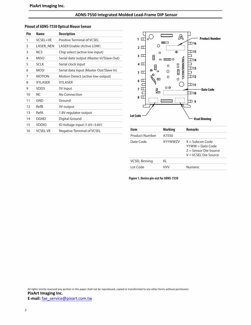
Pinout of ADNS-7550 Optical Mouse Sensor
Pin Name Description
1 VCSEL+VE Positive Terminal of VCSEL
2 LASER_NEN LASER Enable (Active LOW)
3 NCS Chip select (active low input)
4 MISO Serial data output (Master In/Slave Out)
5 SCLK Serial clock input
6 MOSI Serial data input (Master Out/Slave In)
7 MOTION Motion Detect (active low output)
8 XYLASER XYLASER
9 VDD5 5V Input
10 NC No Connection
11 GND Ground
12 RefB 3V output
13 RefA 1.8V regulator output
14 DGND Digital Ground
15 VDDIO IO Voltage input (1.65~3.6V)
16 VCSEL-VE Negative Terminal of VCSEL
Figure 1. Device pin-out for ADNS-7550
Product Number
Vcsel BinningLot Code
Date Code
1
2
3
4
5
6
7
8
16
15
14
13
12
11
10
9
Item Marking Remarks
Product Number A7550
Date Code XYYWWZV X = Subcon CodeYYWW = Date CodeZ = Sensor Die SourceV = VCSEL Die Source
VCSEL Binning KL
Lot Code VVV Numeric
All rights strictly reserved any portion in this paper shall not be reproduced, copied or transformed to any other forms without permission.
PixArt Imaging Inc. E-mail: [email protected]
PixArt Imaging Inc.
ADNS-7550 Integrated Molded Lead-Frame DIP Sensor
3
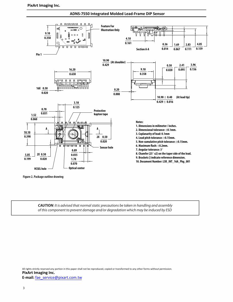
Figure 2. Package outline drawing
CAUTION: It is advised that normal static precautions be taken in handling and assemblyof this component to prevent damage and/or degradation which may be induced by ESD
Section A-A
4.10
0.161 0.36
0.014
1.69
0.067
2.83
0.111
4.05
0.159
AA
Optical center
Protective kapton tape
VCSEL hole
Sensor hole
3.18
0.125
2X 0.50
0.020
0.89
0.035
1.78
0.070
2X 0.50
0.020
0.78
0.0311.52
0.060
5.05
0.199
10.10
0.398
16X 0.50
0.020
16.20
0.638
10.90(At shoulder)
0.429
9.10
0.358
10.90 ± 0.40 (At lead tip)
0.429 ± 0.016
0.20
0.008
0.50
0.020
2.41
0.095
3.96
0.156
Feature For
Illustration Only
Pin 1
9.10
0.358
Notes:
1. Dimensions in milimeter / inches.
2. Dimensional tolerance: ±0.1mm.
3. Coplanarity of lead: 0.1mm
4. Lead pitch tolerance: ±0.15mm.
5. Non-cumulative pitch tolerance: ±0.15mm.
6. Maximum flash: ±0.2mm.
7. Angular tolerance: 3
8. Chamfer (25 x2) on the taper side of the lead.
9. Brackets () indicate reference dimension.
10. Document Number: LSR_INT_16A_Pkg_001
All rights strictly reserved any portion in this paper shall not be reproduced, copied or transformed to any other forms without permission.
PixArt Imaging Inc. E-mail: [email protected]
PixArt Imaging Inc.
ADNS-7550 Integrated Molded Lead-Frame DIP Sensor
4
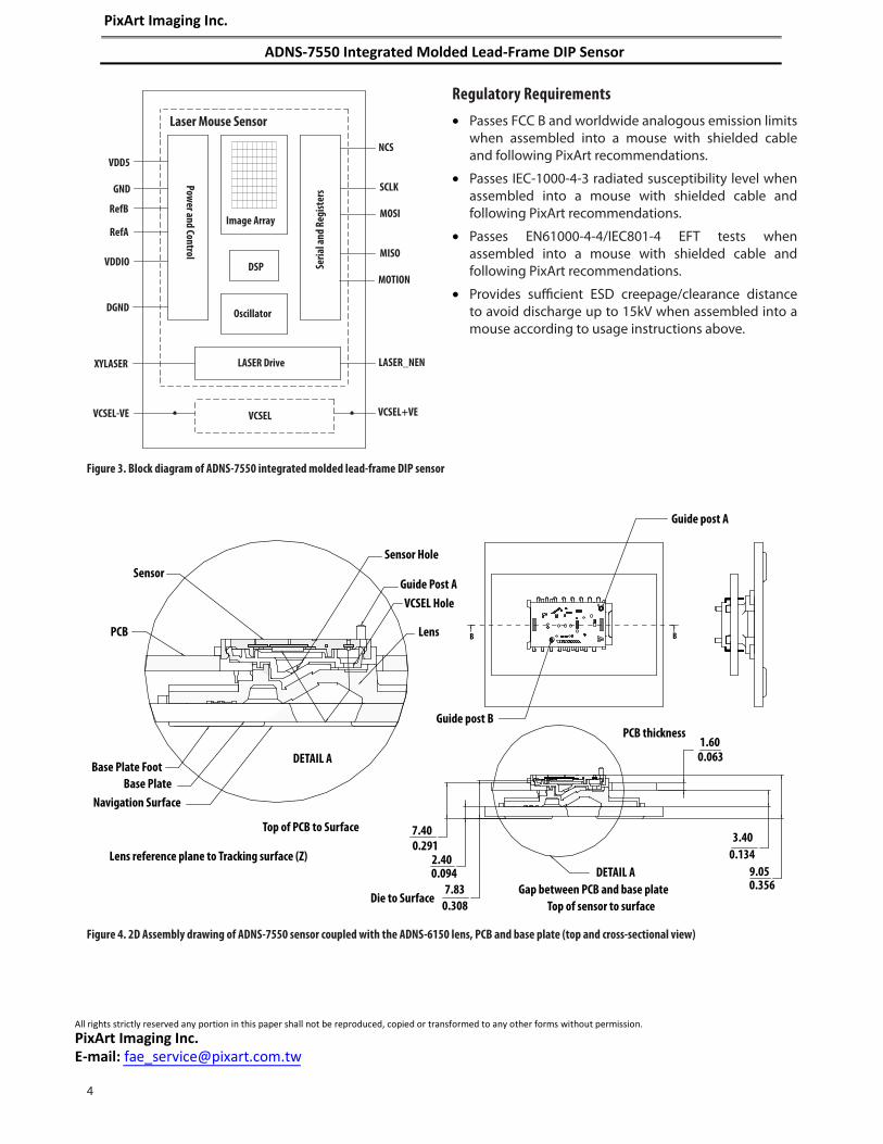
Figure 3. Block diagram of ADNS-7550 integrated molded lead-frame DIP sensor
Regulatory Requirements
• Passes FCC B and worldwide analogous emission limits when assembled into a mouse with shielded cable and following PixArt recommendations.
• Passes IEC-1000-4-3 radiated susceptibility level when assembled into a mouse with shielded cable and following PixArt recommendations.
• Passes EN61000-4-4/IEC801-4 EFT tests when assembled into a mouse with shielded cable and following PixArt recommendations.
• Provides suffi cient ESD creepage/clearance distance to avoid discharge up to 15kV when assembled into a mouse according to usage instructions above.
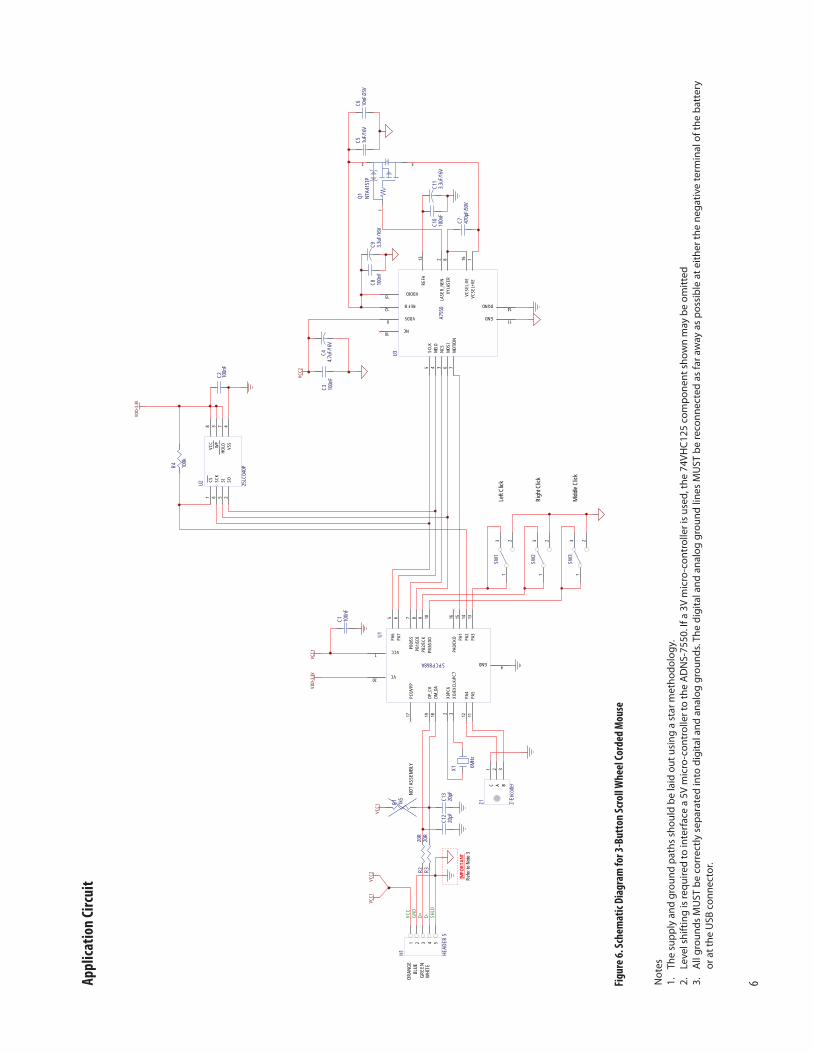
Figure 4. 2D Assembly drawing of ADNS-7550 sensor coupled with the ADNS-6150 lens, PCB and base plate (top and cross-sectional view)
Oscillator
LASER Drive
MISO
MOTION
MOSI
LASER_NEN
VCSEL+VE
XYLASER
VCSEL-VE
DGND
VDDIO
GND
VDD5
RefA
Pow
er and Con
trol
Image Array
DSP
VCSEL
Laser Mouse Sensor
Seri
al a
nd
Reg
iste
rs
SCLK
NCS
RefB
DETAIL A
Top of PCB to Surface 7.40
0.291Lens reference plane to Tracking surface (Z) 2.40
0.094
PCB thickness1.60
0.063
Gap between PCB and base plate
3.40
0.134
Top of sensor to surface
9.050.356
Die to Surface7.83
0.308
DETAIL A
Sensor Hole
Guide Post A
VCSEL Hole
Lens
Sensor
PCB
Base Plate Foot
Base Plate
Navigation Surface
B B
Guide post A
Guide post B
All rights strictly reserved any portion in this paper shall not be reproduced, copied or transformed to any other forms without permission.
PixArt Imaging Inc. E-mail: [email protected]
PixArt Imaging Inc.
ADNS-7550 Integrated Molded Lead-Frame DIP Sensor

5
Figure 5. Recommended PCB mechanical cutouts and spacing
Assembly Recommendation
1. Insert the integrated molded lead-frame DIP sensor and all other electrical components into the application PCB.
2. This sensor package is only qualifi ed for wave-solder process.
3. Wave-solder the entire assembly in a no-wash solder process utilizing a solder fi xture. The solder fi xture is needed to protect the sensor during the solder process. The fi xture should be designed to expose the sensor leads to solder while shielding the optical aperture from direct solder contact.
4. Place the lens onto the base plate. Care must be taken to avoid contamination on the optical surfaces.
5. Remove the protective kapton tapes from the optical aperture of the sensor and VCSEL respectively. Care must be taken to keep contaminants from entering the aperture.
6. Insert the PCB assembly over the lens onto the base plate. The sensor package should self-align to the lens. The optical position reference for the PCB is set by the base plate and lens. The alignment guide post of the lens locks the lens and integrated molded lead-frame DIP sensor together. Note that the PCB motion due to button presses must be minimized to maintain optical alignment.
7. Optional: The lens can be permanently locked to the sensor package by melting the lens’ guide posts over the sensor with heat staking process.
8. Tune the laser output power from the VCSEL to meet the Eye Safe Class I Standard as detailed in the LASER Power Adjustment Procedure.
9. Install the mouse top case. There must be a feature in the top case (or other area) to press down onto the sensor to ensure the sensor and lenses are interlocked to the correct vertical height.
Design considerations for improving ESD Performance
For improved electrostatic discharge performance, typical creepage and clearance distance are shown in the table below. Assumption: base plate construction as per the PixArt supplied IGES fi le and ADNS-6150, ADNS-6160-001 or ADNS-6170-002 lens:
Lens ADNS-6150 ADNS-6160-001 ADNS-6170-002
Creepage 12.0 mm 13.50 mm 20.30 mm
Clearance 2.1 mm 1.28 mm 1.28 mm
Note that the lens material is polycarbonate and therefore, cyanoacrylate based adhesives or other adhesives that may damage the lens should NOT be used.
Optical center
Pin #1
7X 1.78
0.070
0.89
0.035
3.18
0.125
5.35
0.21
1
Lens interference 2.31
0.091
13.35
0.526
10.7
0
0.42
1
(2.78)
0.110
1.05
0.04
19.
65
0.38
0
14.18
0.558
∅ 1.10 Pad ring
0.043
16X ∅ 0.70
0.028
0
0
All rights strictly reserved any portion in this paper shall not be reproduced, copied or transformed to any other forms without permission.
PixArt Imaging Inc. E-mail: [email protected]
PixArt Imaging Inc.
ADNS-7550 Integrated Molded Lead-Frame DIP Sensor
6
VCC
D+
D-
GN
D
SHLD
1 2 3 4 5
H1
HEA
DER
5
OR
ANG
EBL
UE
GR
EEN
WH
ITE
VCC
1
C5
1uF/
16V
C6
10nF
/25V
2
1
3
Q1
NTA
4151
P
C3
100n
FVCC
2
C4
4.7u
F/16
V
C7
470p
F/50
V
VDD
-3.3
V
C1
100n
F
VCC
1
Mid
dle
Clic
k
Rig
ht C
lick
Left
Clic
k
VCC1
XI/P
C6
2
XO/E
XCLK
/PC
73
GND4
PB0/
SS7
PB1/
SDI
8
PB2/
SCK
9
PB3/
SDO
10
PA3
13PA
214
PA1
15PA
0/C
KO16
PC0/
VPP
17
DM
_DA
18D
P_C
K19
VC20
PA7
6PA
65
PA5
11PA
412
U1
SPCP868A
CS
1
SO2
WP
3
VSS
4SI
5SC
K6
HO
LD7
VCC
8U
2
25LC
040P
C2
100n
F
R4
100k
VDD
-3.3
V
VCC
2C
810
0nF
C9
3.3u
F/16
V
C10
100n
FC
113.
3uF/
16V
A2
B3
C1
Z1 Z-En
code
r
13 2
SW1
13 2
SW2
13 2
SW3
X1 6MH
z
C12
20pF
C13
20pF
R1
1k5
VCC
1
R3
20R
R2
20R
NO
T AS
SEM
BLY
IMPO
RTA
NT
Ref
er to
Not
e 3
NC10
VDD59
VDDIO15
REF
A13
LASE
R_N
EN2
VCSE
L+VE
1
SCLK
5
MIS
O4
MO
SI6
NCS
3
MO
TIO
N7
VCSE
L-VE
16
XYLA
SER
8
DGND14
REF B12
GND11
U3
A755
0
Ap
pli
cati
on C
ircu
it
Figu
re 6
. Sch
emat
ic D
iagr
am fo
r 3-
Bu
tton
Scr
oll W
hee
l Cor
ded
Mou
se
Not
es
1.
The
supp
ly a
nd g
roun
d pa
ths
shou
ld b
e la
id o
ut u
sing
a s
tar m
etho
dolo
gy.
2.
Leve
l shi
ftin
g is
requ
ired
to in
terf
ace
a 5V
mic
ro-c
ontr
olle
r to
the
AD
NS-
7550
. If a
3V
mic
ro-c
ontr
olle
r is
used
, the
74V
HC1
25 c
ompo
nent
sho
wn
may
be
omitt
ed3.
A
ll gr
ound
s M
UST
be
corr
ectly
sep
arat
ed in
to d
igita
l and
ana
log
grou
nds.
The
digi
tal a
nd a
nalo
g gr
ound
line
s M
UST
be
reco
nnec
ted
as fa
r aw
ay a
s po
ssib
le a
t eith
er th
e ne
gativ
e te
rmin
al o
f the
bat
tery
or
at t
he U
SB c
onne
ctor
.

7
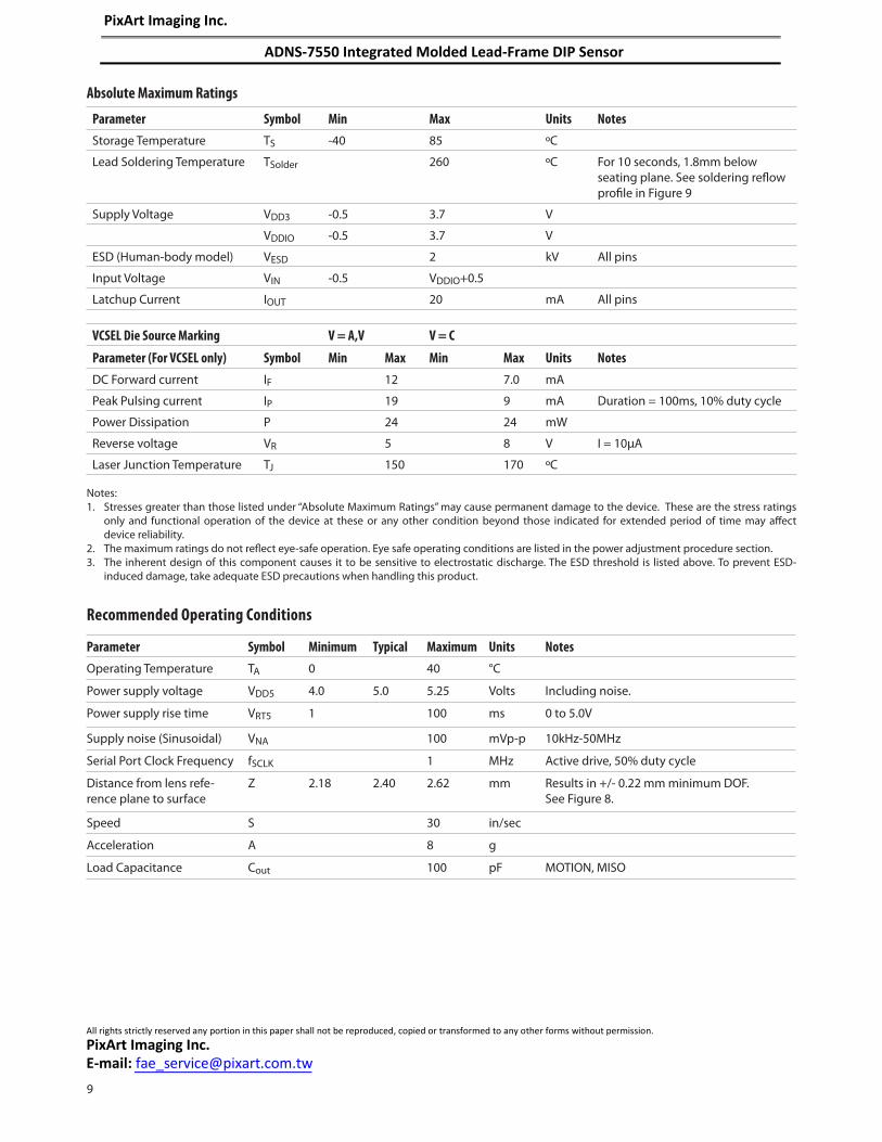
LASER Drive Mode
The laser is driven in pulsed mode during normal operation. A calibration mode is provided which drives the laser in continuous (CW) operation.
Eye Safety
The ADNS-7550 integrated molded lead-frame DIP sensor and the associated components in the schematic of Figure 5 are intended to comply with Class 1 Eye Safety Requirements of IEC 60825-1. PixArt Imaging suggests that manufacturers perform testing to verify eye safety on each mouse. It is also recommended to review possible single fault mechanisms beyond those described below in the section “Single Fault Detection”. Under normal conditions, the sensor generates the drive current for the VCSEL.
In order to stay below the Class 1 power requirements, LASER_CTRL0 (register 0x1a), LASER_CTRL1 (register 0x1f ), LSRPWR_CFG0 (register 0x1c) and LSRPWR_CFG1 (register 0x1d) must be programmed to appropriate values. The ADNS-7550 integrated molded lead-frame DIP sensor which comprised of the sensor and VCSEL; is designed to maintain the output beam power within Class 1 requirements over components manufacturing tolerances and the recommended temperature range when adjusted per the procedure below and implement-ed as shown in the recommended application circuit of Figure 6. For more information, please refer to Eye Safety Application Note AN 5361.
LASER Power Adjustment Procedure
1. The ambient temperature should be 25C +/- 5C.
2. Set VDD5 to its permanent value.
3. Set the Range bits (bit 7 and 6 of register 0x1f ) to b’01.
4. Set the Range_C1 and Range_C0 complement bits (bit 7 and 6 of register 0x1f ) to b’10.
5. Enable the Calibration mode by writing to bits [3, 2, 1] of register 0x1A so the laser will be driven with 100% duty cycle.
6. Set the laser current to the minimum value by writing 0x00 to register 0x1c, and the complementary value 0xFF to register 0x1d.
7. Program registers 0x1c and 0x1d with increasing values to achieve an output power of not more than 506uW to meet class 1 Eye Safety over temperature. If this power is obtained, the calibration is complete, skip to step 11.
8. If it was not possible to achieve the power target, set the laser current to the minimum value by writing 0x00 to register 0x1c, and the complementary value 0xff to register 0x1d.
9. Set the Range and Range_C bits in registers 0x1a and 0x1f, respectively, to choose to the higher laser current range.
10. Program registers 0x1c and 0x1d with increasing values to achieve an output power of not more than 506uW to meet class 1 Eye Safety over temperature.
11. Save the value of registers 0x1a, 0x1c, 0x1d, and 0x1f in non-volatile memory in the mouse. These registers must be restored to these values every time the ADNS-7550 is reset.
12. Reset the mouse, reload the register values from non-volatile memory, enable Calibration mode, and measure the laser power to verify that the calibration is correct.
Good engineering practices such as regular power meter calibration, random quality assurance retest of calibrated mice, etc. should be used to guarantee performance, reli-ability and safety for the product design.
LASER Output Power
The laser beam output power as measured at the naviga-tion surface plane is specifi ed below. The following con-ditions apply:
1. The system is adjusted according to the above procedure.
2. The system is operated within the recommended operating temperature range.
3. No allowance for optical power meter accuracy is assumed.
All rights strictly reserved any portion in this paper shall not be reproduced, copied or transformed to any other forms without permission.
PixArt Imaging Inc. E-mail: [email protected]
PixArt Imaging Inc.
ADNS-7550 Integrated Molded Lead-Frame DIP Sensor

8
Disabling the LASER
LASER_NEN is connected to the gate of a P-channel MOSFET transistor which when ON connects RefB to the LASER. In normal operation, LASER_NEN is low. In the case of a fault condition (ground or RefB at XYLASER), LASER_NEN goes high to turn the transistor off and dis-connect RefB from the LASER.
Single Fault Detection
ADNS-7550 is able to detect a short circuit or fault condition at the XYLASER pin, which could lead to excessive laser power output. A path to ground on this
pin will trigger the fault detection circuit, which will turn off the laser drive current source and set the LASER_NEN output high. When used in combination with external components as shown in the block diagram below, the system will prevent excess laser power for a resistive path to ground at XYLASER by shutting off the laser. In addition to the ground path fault detection described above, the fault detection circuit is continuously checking for proper operation by internally generating a path to ground with the laser turned off via LASER_NEN. If the XYLASER pin is shorted to VDD5/RefA/RefB, this test will fail and will be reported as a fault.
Figure 7. Single Fault Detection and Eye-safety Feature Block Diagram
LASERDRIVER
fault controlblock
VCSEL
VDD3
GND
voltage sensor
Microcontroller
Serial port
VCSEL+VE
VCSEL-VE
XYLASER
LASER_NEN
Ref B
current set
ADNS-7550
D
SG
All rights strictly reserved any portion in this paper shall not be reproduced, copied or transformed to any other forms without permission.
PixArt Imaging Inc. E-mail: [email protected]
PixArt Imaging Inc.
ADNS-7550 Integrated Molded Lead-Frame DIP Sensor
9
Absolute Maximum Ratings
Parameter Symbol Min Max Units Notes
Storage Temperature TS -40 85 ºC
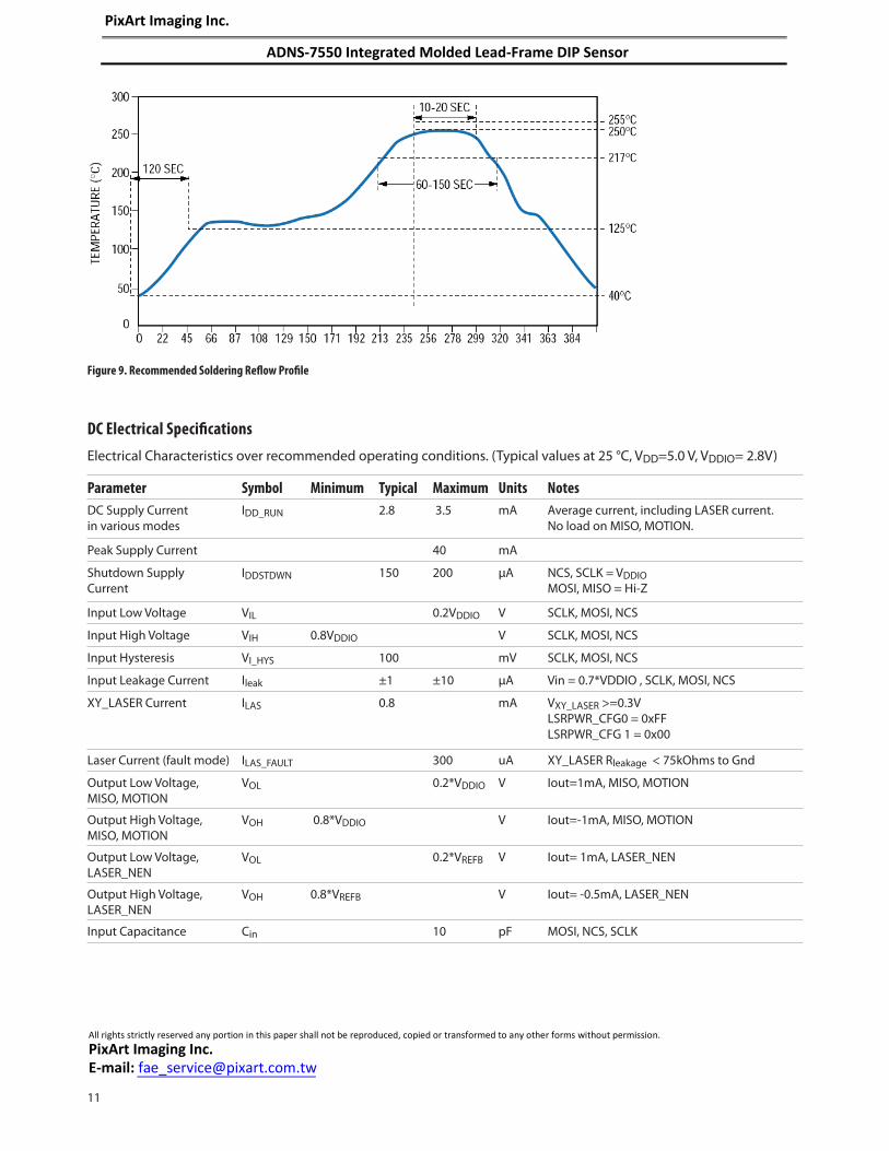
Lead Soldering Temperature TSolder 260 ºC For 10 seconds, 1.8mm below seating plane. See soldering refl ow profi le in Figure 9
Supply Voltage VDD3 -0.5 3.7 V
VDDIO -0.5 3.7 V
ESD (Human-body model) VESD 2 kV All pins
Input Voltage VIN -0.5 VDDIO+0.5
Latchup Current IOUT 20 mA All pins
VCSEL Die Source Marking V = A,V V = C
Parameter (For VCSEL only) Symbol Min Max Min Max Units Notes
DC Forward current IF 12 7.0 mA
Peak Pulsing current IP 19 9 mA Duration = 100ms, 10% duty cycle
Power Dissipation P 24 24 mW
Reverse voltage VR 5 8 V I = 10μA
Laser Junction Temperature TJ 150 170 ºC
Notes:1. Stresses greater than those listed under “Absolute Maximum Ratings” may cause permanent damage to the device. These are the stress ratings
only and functional operation of the device at these or any other condition beyond those indicated for extended period of time may aff ect device reliability.
2. The maximum ratings do not refl ect eye-safe operation. Eye safe operating conditions are listed in the power adjustment procedure section.3. The inherent design of this component causes it to be sensitive to electrostatic discharge. The ESD threshold is listed above. To prevent ESD-
induced damage, take adequate ESD precautions when handling this product.
Recommended Operating Conditions
Parameter Symbol Minimum Typical Maximum Units Notes
Operating Temperature TA 0 40 °C
Power supply voltage VDD5 4.0 5.0 5.25 Volts Including noise.
Power supply rise time VRT5 1 100 ms 0 to 5.0V
Supply noise (Sinusoidal) VNA 100 mVp-p 10kHz-50MHz
Serial Port Clock Frequency fSCLK 1 MHz Active drive, 50% duty cycle
Distance from lens refe-rence plane to surface
Z 2.18 2.40 2.62 mm Results in +/- 0.22 mm minimum DOF.See Figure 8.
Speed S 30 in/sec
Acceleration A 8 g
Load Capacitance Cout 100 pF MOTION, MISO
All rights strictly reserved any portion in this paper shall not be reproduced, copied or transformed to any other forms without permission.
PixArt Imaging Inc. E-mail: [email protected]
PixArt Imaging Inc.
ADNS-7550 Integrated Molded Lead-Frame DIP Sensor
10
Figure 8. Distance from lens reference plane to surface, Z
Sensor
Lens
Navigation SurfaceLens to Surface 2.40
Optical/Electrical Characteristics (at Tc = 5°C to 45°C):
VCSEL Die Source Marking V = A,V V = C
Parameter Symbol Min Typ Max Min Typ Max Units Notes
Peak Wavelength λ 832 865 832 865 nm
Maximum Radiant Power
LOPmax 4.5 4.0 mW Maximum output power under any condition. This is not a recommended operating condition and does not meet eye safety requirements.
Wavelength Temperature coef-fi cient
dλ/dT 0.065 0.065 nm/ºC
Wavelength Current coeffi cient
dλ/dI 0.21 0.3 nm/mA
Beam Divergence θFW@1/e^2
15 16 deg
Threshold current Ith 4.2 3.0 mA
Slope Effi ciency SE 0.4 0.35 W/A
Forward Voltage VF 2.1 2.4 2.1 2.4 V At 500uW output power
Comments: 1. VCSELs are sorted into bins as specifi ed in the power adjustment procedure. Appropriate binning register data values are used in the application
circuit to achieve the target output power. The VCSEL binning is marked on the integrated molded lead-frame DIP sensor package.2. When driven with current or temperature range greater than specifi ed in the power adjustment procedure section, eye safety limits may be
exceeded. The VCSEL should then be treated as a Class IIIb laser and as a potential eye hazard.3. Over driving beyond LOPmax limit will cause the VSCEL to enter into on unstable region. Any LOP reference point in the laser power calibration
process.
All rights strictly reserved any portion in this paper shall not be reproduced, copied or transformed to any other forms without permission.
PixArt Imaging Inc. E-mail: [email protected]
PixArt Imaging Inc.
ADNS-7550 Integrated Molded Lead-Frame DIP Sensor
11
DC Electrical Specifi cations
Electrical Characteristics over recommended operating conditions. (Typical values at 25 °C, VDD=5.0 V, VDDIO= 2.8V)
Parameter Symbol Minimum Typical Maximum Units Notes
DC Supply Currentin various modes
IDD_RUN 2.8 3.5 mA Average current, including LASER current.No load on MISO, MOTION.
Peak Supply Current 40 mA
Shutdown SupplyCurrent
IDDSTDWN 150 200 μA NCS, SCLK = VDDIOMOSI, MISO = Hi-Z
Input Low Voltage VIL 0.2VDDIO V SCLK, MOSI, NCS
Input High Voltage VIH 0.8VDDIO V SCLK, MOSI, NCS
Input Hysteresis VI_HYS 100 mV SCLK, MOSI, NCS
Input Leakage Current Ileak ±1 ±10 μA Vin = 0.7*VDDIO , SCLK, MOSI, NCS
XY_LASER Current ILAS 0.8 mA VXY_LASER >=0.3VLSRPWR_CFG0 = 0xFFLSRPWR_CFG 1 = 0x00
Laser Current (fault mode) ILAS_FAULT 300 uA XY_LASER Rleakage < 75kOhms to Gnd
Output Low Voltage,MISO, MOTION
VOL 0.2*VDDIO V Iout=1mA, MISO, MOTION
Output High Voltage,MISO, MOTION
VOH 0.8*VDDIO V Iout=-1mA, MISO, MOTION
Output Low Voltage,LASER_NEN
VOL 0.2*VREFB V Iout= 1mA, LASER_NEN
Output High Voltage,LASER_NEN
VOH 0.8*VREFB V Iout= -0.5mA, LASER_NEN
Input Capacitance Cin 10 pF MOSI, NCS, SCLK
Figure 9. Recommended Soldering Refl ow Profi le
All rights strictly reserved any portion in this paper shall not be reproduced, copied or transformed to any other forms without permission.
PixArt Imaging Inc. E-mail: [email protected]
PixArt Imaging Inc.
ADNS-7550 Integrated Molded Lead-Frame DIP Sensor
12
AC Electrical Specifi cations
Electrical Characteristics over recommended operating conditions. (Typical values at 25 °C, VDD=5.0V, VDDIO= 2.8V)
Parameter Symbol Minimum Typical Maximum Units Notes
Motion delayafter reset
tMOT-RST 23 ms From SW_RESET register write to valid motion, assuming motion is present
Shutdown tSTDWN 50 ms From Shutdown mode active to low current
Wake fromshutdown
tWAKEUP 23 ms From Shutdown mode inactive to valid motion. Notes: A RESET must be asserted after a shutdown. Refer to section “Notes on Shutdown also note tMOT-RST
MISO rise time tr-MISO 150 300 ns CL = 100pF
MISO fall time tf-MISO 150 300 ns CL = 100pF
MISO delayafter SCLK
tDLY-MISO 120 ns From SCLK falling edge to MISO data valid, no load conditions
MISO hold time thold-MISO 0.5 1/fSCLK us Data held until next falling SCLK edge
MOSI hold time thold-MOSI 200 ns Amount of time data is valid after SCLK rising edge
MOSI setup time tsetup-MOSI 120 ns From data valid to SCLK rising edge
SPI time betweenwrite commands
tSWW 30 μs From rising SCLK for last bit of the fi rst data byte, to rising SCLK for last bit of the second data byte.
SPI time betweenwrite and readcommands
tSWR 20 μs From rising SCLK for last bit of the fi rst data byte, to rising SCLK for last bit of the second address byte.
SPI time betweenread and subsequent commands
tSRWtSRR
500 ns From rising SCLK for last bit of the fi rst data byte, to falling SCLK for the fi rst bit of the address byte of the next command.
SPI read address-data delay
tSRAD 4 μs From rising SCLK for last bit of the address byte, to falling SCLK for fi rst bit of data being read.
NCS inactive aftermotion burst
tBEXIT 500 ns Minimum NCS inactive time after motion burst before next SPI usage
NCS to SCLK active tNCS-SCLK 120 ns From NCS falling edge to fi rst SCLK rising edge
SCLK to NCS inactive(for read operation)
tSCLK-NCS 120 ns From last SCLK rising edge to NCS rising edge, for valid MISO data transfer
SCLK to NCS inactive(for write operation)
tSCLK-NCS 20 us From last SCLK rising edge to NCS rising edge, for valid MOSI data transfer
NCS to MISO high-Z tNCS-MISO 500 ns From NCS rising edge to MISO high-Z state
MOTION rise time tr-MOTION 150 300 ns CL = 100pF
MOTION fall time tf-MOTION 150 300 ns CL = 100pF
Transient SupplyCurrent
IDDT 45 mA Max supply current during a VDD ramp from 0 to 2.8V
All rights strictly reserved any portion in this paper shall not be reproduced, copied or transformed to any other forms without permission.
PixArt Imaging Inc. E-mail: [email protected]
PixArt Imaging Inc.
ADNS-7550 Integrated Molded Lead-Frame DIP Sensor

13
Typical Path Deviation Largest Single Perpendicular Deviation
From A Straight Line at 45 Degrees Path Length = 4 inches;
Speed = 6 ips; Resolution = 800cpi
-5
5
15
25
35
45
-0.3 -0.2 -0.1 0 0.1 0.2 0.3Z - Height(mm)
Mou
se C
oun
t
White Paper
Photo Paper
Manila
Spruce Wood
Black Formica
White Formica
White Delrin
Figure 11. Average Error vs. Distance at 800cpi (mm)
Resolution vs Z- Height on General Surfaces (A7550)
0
200
400
600
800
1000
1200
-0.3 -0.2 -0.1 0 0.1 0.2 0.3
Z-Height(mm)
Res
olu
tion
(DP
I)
White Paper
Photo Paper
Manila
Spruce Wood
Black Formica
White Formica
White Delrin
Figure 10. Mean Resolution vs. Z at 800cpi
All rights strictly reserved any portion in this paper shall not be reproduced, copied or transformed to any other forms without permission.
PixArt Imaging Inc. E-mail: [email protected]
PixArt Imaging Inc.
ADNS-7550 Integrated Molded Lead-Frame DIP Sensor
14
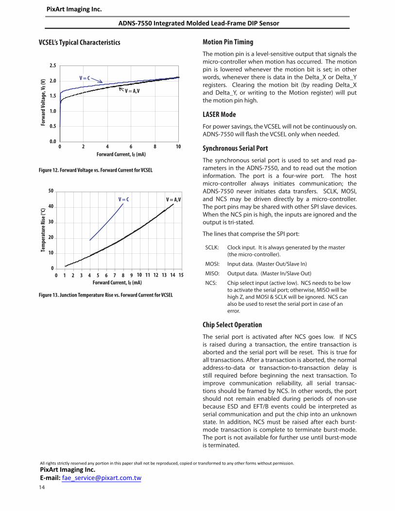
Figure 12. Forward Voltage vs. Forward Current for VCSEL
Figure 13. Junction Temperature Rise vs. Forward Current for VCSEL
VCSEL’s Typical Characteristics Motion Pin Timing
The motion pin is a level-sensitive output that signals the micro-controller when motion has occurred. The motion pin is lowered whenever the motion bit is set; in other words, whenever there is data in the Delta_X or Delta_Y registers. Clearing the motion bit (by reading Delta_X and Delta_Y, or writing to the Motion register) will put the motion pin high.
LASER Mode
For power savings, the VCSEL will not be continuously on. ADNS-7550 will fl ash the VCSEL only when needed.
Synchronous Serial Port
The synchronous serial port is used to set and read pa-rameters in the ADNS-7550, and to read out the motion information. The port is a four-wire port. The host micro-controller always initiates communication; the ADNS-7550 never initiates data transfers. SCLK, MOSI, and NCS may be driven directly by a micro-controller. The port pins may be shared with other SPI slave devices. When the NCS pin is high, the inputs are ignored and the output is tri-stated.
The lines that comprise the SPI port:
SCLK: Clock input. It is always generated by the master (the micro-controller).
MOSI: Input data. (Master Out/Slave In)
MISO: Output data. (Master In/Slave Out)
NCS: Chip select input (active low). NCS needs to be low to activate the serial port; otherwise, MISO will be high Z, and MOSI & SCLK will be ignored. NCS can also be used to reset the serial port in case of an error.
Chip Select Operation
The serial port is activated after NCS goes low. If NCS is raised during a transaction, the entire transaction is aborted and the serial port will be reset. This is true for all transactions. After a transaction is aborted, the normal address-to-data or transaction-to-transaction delay is still required before beginning the next transaction. To improve communication reliability, all serial transac-tions should be framed by NCS. In other words, the port should not remain enabled during periods of non-use because ESD and EFT/B events could be interpreted as serial communication and put the chip into an unknown state. In addition, NCS must be raised after each burst-mode transaction is complete to terminate burst-mode. The port is not available for further use until burst-mode is terminated.
0.0
0.5
1.0
1.5
2.0
2.5
0 2 4 6 8 10
Forward Current, IF (mA)
Forw
ard
Vol
tage
, VF
(V)
V = A,V
V = C
0
10
20
30
40
50
0 1 2 3 4 5 6 7 8 9 10 11 12 13 14 15
Forward Current, IF (mA)
Tem
pera
ture
Ris
e (°
C)
V = C V = A,V
All rights strictly reserved any portion in this paper shall not be reproduced, copied or transformed to any other forms without permission.
PixArt Imaging Inc. E-mail: [email protected]
PixArt Imaging Inc.
ADNS-7550 Integrated Molded Lead-Frame DIP Sensor
15
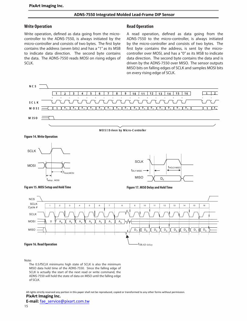
Read Operation
A read operation, defi ned as data going from the ADNS-7550 to the micro-controller, is always initiated by the micro-controller and consists of two bytes. The fi rst byte contains the address, is sent by the micro-controller over MOSI, and has a “0” as its MSB to indicate data direction. The second byte contains the data and is driven by the ADNS-7550 over MISO. The sensor outputs MISO bits on falling edges of SCLK and samples MOSI bits on every rising edge of SCLK.
1 2 3 4 5 6 7 8SCLK
Cycle #
SCLK
MOSI 0 A6 A5 A4 A3 A2 A1 A0
9 10 11 12 13 14 15 16
MISO D6 D5 D4 D3 D2 D1D0D7
NCS
tSRAD delayFigure 16. Read Operation
SCLK
MISO D0
tHOLD-MISO
tDLY-MISO
Figure 17. MISO Delay and Hold Time
Note: The 0.5/fSCLK minimums high state of SCLK is also the minimum
MISO data hold time of the ADNS-7550. Since the falling edge of SCLK is actually the start of the next read or write command, the ADNS-7550 will hold the state of data on MISO until the falling edge of SCLK.
SCLK
MOSI
tsetup , MOSI
tHold,MOSI
Fig ure 15. MOSI Setup and Hold Time
A6
A5
A2
A3
A4
A0
A1
D7
D4
D5
D6
D0
D1
D2
D3
1 57 8 9 1 0 1 1 1 2 1 3 1 4 1 62 3 4 5 6
1
S C L K
M O S I
M O S I D rive n by M icro -C o ntro lle r
1
1
1
A6
2
N C S
M I S O
Figure 14. Write Operation
Write Operation
Write operation, defi ned as data going from the micro-controller to the ADNS-7550, is always initiated by the micro-controller and consists of two bytes. The fi rst byte contains the address (seven bits) and has a “1” as its MSB to indicate data direction. The second byte contains the data. The ADNS-7550 reads MOSI on rising edges of SCLK.
All rights strictly reserved any portion in this paper shall not be reproduced, copied or transformed to any other forms without permission.
PixArt Imaging Inc. E-mail: [email protected]
PixArt Imaging Inc.
ADNS-7550 Integrated Molded Lead-Frame DIP Sensor
16
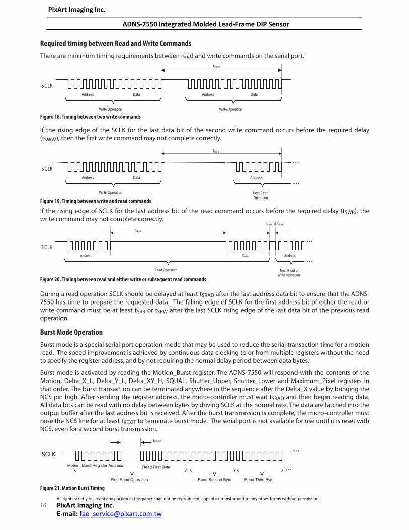
If the rising edge of SCLK for the last address bit of the read command occurs before the required delay (tSWR), the write command may not complete correctly.
Next Read orWrite Operation
Data
tSRAD
Read Operation
Address
tSRW & t SRR
Address
SCLK
Figure 20. Timing between read and either write or subsequent read commands
During a read operation SCLK should be delayed at least tSRAD after the last address data bit to ensure that the ADNS-7550 has time to prepare the requested data. The falling edge of SCLK for the fi rst address bit of either the read or write command must be at least tSRR or tSRW after the last SCLK rising edge of the last data bit of the previous read operation.
Required timing between Read and Write Commands
There are minimum timing requirements between read and write commands on the serial port.
SCLK
Address Data
tSWW
Write Operation
Address Data
Write Operation
Figure 18. Timing between two write commands
If the rising edge of the SCLK for the last data bit of the second write command occurs before the required delay (tSWW), then the fi rst write command may not complete correctly.
Address Data
Write Operation
Address
Next ReadOperation
SCLK
tSWR
Figure 19. Timing between write and read commands
Burst Mode Operation
Burst mode is a special serial port operation mode that may be used to reduce the serial transaction time for a motion read. The speed improvement is achieved by continuous data clocking to or from multiple registers without the need to specify the register address, and by not requiring the normal delay period between data bytes.
Burst mode is activated by reading the Motion_Burst register. The ADNS-7550 will respond with the contents of the Motion, Delta_X_L, Delta_Y_L, Delta_XY_H, SQUAL, Shutter_Upper, Shutter_Lower and Maximum_Pixel registers in that order. The burst transaction can be terminated anywhere in the sequence after the Delta_X value by bringing the NCS pin high. After sending the register address, the micro-controller must wait tSRAD and then begin reading data. All data bits can be read with no delay between bytes by driving SCLK at the normal rate. The data are latched into the output buff er after the last address bit is received. After the burst transmission is complete, the micro-controller must raise the NCS line for at least tBEXIT to terminate burst mode. The serial port is not available for use until it is reset with NCS, even for a second burst transmission.
Motion_Burst Register Address Read First Byte
First Read Operation Read Second Byte
SCLK
tSRAD
Read Third Byte
Figure 21. Motion Burst Timing
All rights strictly reserved any portion in this paper shall not be reproduced, copied or transformed to any other forms without permission.
PixArt Imaging Inc. E-mail: [email protected]
PixArt Imaging Inc.
ADNS-7550 Integrated Molded Lead-Frame DIP Sensor

17
Notes on Power-up
The ADNS-7550 does not perform an internal power up self-reset; the POWER_UP_RESET register must be written every time power is applied. The appropriate sequence is as follows:
i. Apply power to VDD5 and VDDIO in any order, with the delay of no more than 100ms in between each supply. Ensure all supplies are stable.
ii. Drive NCS high, then low to reset the SPI port.
iii. Write 0x5a to register 0x3a.
iv. Wait for at least one frame.
v. Clear observation register.
vi. Wait at least one frame and check observation register, all bits 0-3 must be set.
vii. Read from registers 0x02, 0x03, 0x04 and 0x05 (or read these same 4 bytes from burst motion register 0x42) one time regardless of the motion pin state.
viii. Write 0x27 to register 0x3C
ix. Write 0x0a to register 0x22
x. Write 0x01 to register 0x21
xi. Write 0x32 to register 0x3C
xii. Write 0x20 to register 0x23
xiii. Write 0x05 to register 0x3C
xiv. Write 0xB9 to register 0x37
During power-up there will be a period of time after the power supply is high but before any clocks are available. The table below shows the state of the various pins during power-up and reset.
State of Signal Pins After VDD is Valid
Pin
On
Power-Up
Before Reset
After ResetNCS High NCS Low
NCS Functional Hi Low Functional
MISO Undefi ned Undefi ned FunctionalDepends on NCS
SCLK Ignored Ignored FunctionalDepends on NCS
MOSI Ignored Ignored FunctionalDepends on NCS
MOTION Undefi ned Undefi ned Undefi ned Functional
LASER_NEN Undefi ned Undefi ned Undefi ned Functional
Notes on Shutdown
The ADNS-7550 can be set in Shutdown mode by writing 0xe7 to register 0x3b. The SPI port should not be accessed when Shutdown mode is asserted, except the power-up command (writing 0x5a to register 0x3a). (Other ICs on the same SPI bus can be accessed, as long as the sensor’s NCS pin is not asserted.) The table below shows the state of various pins during shutdown. To deassert Shutdown mode:
i. Write 0x5a to register 0x3a
ii. Wait for at least one frame.
iii. Clear observation register.
iv. Wait at least one frame
v. Check observation register, all bits 0-3 must be set to 1.
vi. Write 0x27 to register 0x3C
vii. Write 0x0a to register 0x22
viii. Write 0x01 to register 0x21
ix. Write 0x32 to register 0x3C
x. Write 0x20 to register 0x23
xi. Write 0x05 to register 0x3C
xii. Write 0xB9 to register 0x37
xiii. Any register settings must then be reloaded.
Pin Status when Shutdown Mode
NCS Functional [1]
MISO Undefi ned [2]
SCLK Ignore if NCS = 1 [3]
MOSI Ignore if NCS = 1 [4]
LASER_NEN High(off )
MOTION Undefi ned [2]
1. NCS pin must be held to 1 (high) if SPI bus is shared with other devices. It is recommended to hold to 1 (high) during Power Down unless powering up the Sensor. It must be held to 0 (low) if the sensor is to be re-powered up from shutdown (writing 0x5a to register 0x3a).
2. Depend on last state3. SCLK is ignore if NCS is 1 (high). It is functional if NCS is 0 (low).4. MOSI is ignore if NCS is 1 (high). If NCS is 0 (low), any command
present on the MOSI pin will be ignored except power-up command (writing 0x5a to register 0x3a).
Note: There are long wakeup times from shutdown. These features should
not be used for power management during normal mouse motion.
All rights strictly reserved any portion in this paper shall not be reproduced, copied or transformed to any other forms without permission.
PixArt Imaging Inc. E-mail: [email protected]
PixArt Imaging Inc.
ADNS-7550 Integrated Molded Lead-Frame DIP Sensor

18
Registers
The ADNS-7550 registers are accessible via the serial port. The registers are used to read motion data and status as well as to set the device confi guration.
Address Register Read/Write Default Value
0x00 Product_ID R 0x32
0x01 Revision_ID R 0x03
0x02 Motion R/W 0x00
0x03 Delta_X_L R 0x00
0x04 Delta_Y_L R 0x00
0x05 Delta_XY_H R 0x00
0x06 SQUAL R 0x00
0x07 Shutter_Upper R 0x00
0x08 Shutter_Lower R 0x64
0x09 Maximum_Pixel R 0xd0
0x0a Pixel_Sum R 0x80
0x0b Minimum_Pixel R 0x00
0x0c CRC0 R 0x00
0x0d CRC1 R 0x00
0x0e CRC2 R 0x00
0x0f CRC3 R 0x00
0x10 Self_Test W NA
0x11 Reserved
0x12 Confi guration2_Bits R/W 0x28
0x13-0x19 Reserved
0x1a LASER_CTRL0 R/W 0x00
0x1b Reserved
0x1c LSRPWR_CFG0 R/W 0x00
0x1d LSRPWR_CFG1 R/W 0x00
0x1e Reserved
0x1f LASER_CTRL1 R/W 0x00
0x20-0x2d Reserved
0x2e Observation R/W 0x00
0x2f-0x34 Reserved
0x35 Pixel_Grab R/W 0x00
0x36 H_RESOLUTION R/W 0x04
0x37-0x39 Reserved
0x3a POWER_UP_RESET W NA
0x3b Shutdown W NA
0x3c Reserved
0x3d Shut_thr R/W 0x56
0x3e Inverse_Revision_ID R 0xfc
0x3f Inverse_Product_ID R 0xcd
0x42 Motion_Burst R 0x00
PixArt Imaging Inc.
ADNS-7550 Integrated Molded Lead-Frame DIP Sensor

19
Product_ID Address: 0x00
Access: Read Reset Value: 0x32
Data Type: 8-Bit unsigned integer
USAGE: This register contains a unique identifi cation assigned to the ADNS-7550. The value in this register does not change; it can be used to verify that the serial communications link is functional.
Bit 7 6 5 4 3 2 1 0
Field PID7 PID6 PID5 PID4 PID3 PID2 PID1 PID0
Bit 7 6 5 4 3 2 1 0
Field RID7 RID6 RID5 RID4 RID3 RID2 RID1 RID0
Revision_ID Address: 0x01
Access: Read Reset Value: 0x03
Data Type: 8-Bit unsigned integer.
USAGE: This register contains the IC revision. It is subject to change when new IC versions are released.
All rights strictly reserved any portion in this paper shall not be reproduced, copied or transformed to any other forms without permission.
PixArt Imaging Inc. E-mail: [email protected]
PixArt Imaging Inc.
ADNS-7550 Integrated Molded Lead-Frame DIP Sensor
20
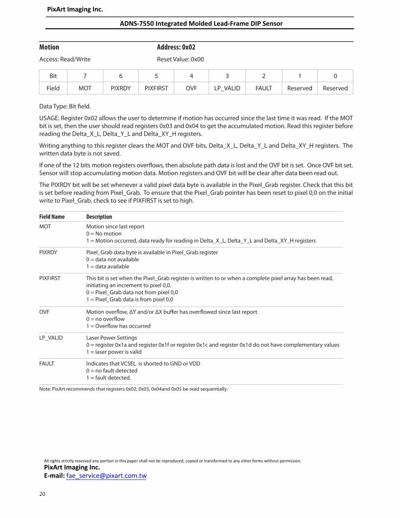
Field Name Description
MOT Motion since last report0 = No motion1 = Motion occurred, data ready for reading in Delta_X_L, Delta_Y_L and Delta_XY_H registers
PIXRDY Pixel_Grab data byte is available in Pixel_Grab register0 = data not available1 = data available
PIXFIRST This bit is set when the Pixel_Grab register is written to or when a complete pixel array has been read, initiating an increment to pixel 0,0.0 = Pixel_Grab data not from pixel 0,01 = Pixel_Grab data is from pixel 0,0
OVF Motion overfl ow, ΔY and/or ΔX buff er has overfl owed since last report0 = no overfl ow1 = Overfl ow has occurred
LP_VALID Laser Power Settings0 = register 0x1a and register 0x1f or register 0x1c and register 0x1d do not have complementary values1 = laser power is valid
FAULT Indicates that VCSEL is shorted to GND or VDD0 = no fault detected1 = fault detected.
Note: PixArt recommends that registers 0x02, 0x03, 0x04and 0x05 be read sequentially.
Bit 7 6 5 4 3 2 1 0
Field MOT PIXRDY PIXFIRST OVF LP_VALID FAULT Reserved Reserved
Motion Address: 0x02
Access: Read/Write Reset Value: 0x00
Data Type: Bit fi eld.
USAGE: Register 0x02 allows the user to determine if motion has occurred since the last time it was read. If the MOT bit is set, then the user should read registers 0x03 and 0x04 to get the accumulated motion. Read this register before reading the Delta_X_L, Delta_Y_L and Delta_XY_H registers.
Writing anything to this register clears the MOT and OVF bits, Delta_X_L, Delta_Y_L and Delta_XY_H registers. The written data byte is not saved.
If one of the 12 bits motion registers overfl ows, then absolute path data is lost and the OVF bit is set. Once OVF bit set, Sensor will stop accumulating motion data. Motion registers and OVF bit will be clear after data been read out.
The PIXRDY bit will be set whenever a valid pixel data byte is available in the Pixel_Grab register. Check that this bit is set before reading from Pixel_Grab. To ensure that the Pixel_Grab pointer has been reset to pixel 0,0 on the initial write to Pixel_Grab, check to see if PIXFIRST is set to high.
All rights strictly reserved any portion in this paper shall not be reproduced, copied or transformed to any other forms without permission.
PixArt Imaging Inc. E-mail: [email protected]
PixArt Imaging Inc.
ADNS-7550 Integrated Molded Lead-Frame DIP Sensor

21
Delta_X_L Address: 0x03
Access: Read Reset Value: 0x00
Data Type: Eight bit 2’s complement number.
USAGE: X movement is counts since last report. Absolute value is determined by resolution. Reading clears the register.
Bit 7 6 5 4 3 2 1 0
Field X7 X6 X5 X4 X3 X2 X1 X0
Bit 7 6 5 4 3 2 1 0
Field Y7 Y6 Y5 Y4 Y3 Y2 Y1 Y0
Delta_Y_L Address: 0x04
Access: Read Reset Value: 0x00
Data Type: Eight bit 2’s complement number.
USAGE: Y movement is counts since last report. Absolute value is determined by resolution. Reading clears the register.
00 01 02 7FE 7FF
+2047+2046+1 +2
FFFE801800
0-1-2-2047-2048Motion
Delta_X
00 01 02 7FE 7FF
+2047+2046+1 +2
FFFE801800
0-1-2-2047-2048Motion
Delta_Y
NOTE: PixArt recommends that registers 0x02, 0x03, 0x04 and 0x05 be read sequentially.
NOTE: PixArt recommends that registers 0x02, 0x03, 0x04 and 0x05 be read sequentially.
Bit 7 6 5 4 3 2 1 0
Field X11 X10 X9 X8 Y11 Y10 Y9 Y8
Delta_XY_H Address: 0x05
Access: Read Reset Value: 0x00
Data Type: 2’s complement number, upper 4 bits of Delta_X and Delta_Y.
USAGE: Delta_XY_H must be read after Delta_X_L and Delta_Y_L to have the full motion data. Reading clear the registers.
NOTE: PixArt recommends that registers 0x02, 0x03, 0x04 and 0x05 be read sequentially.
All rights strictly reserved any portion in this paper shall not be reproduced, copied or transformed to any other forms without permission.
PixArt Imaging Inc. E-mail: [email protected]
PixArt Imaging Inc.
ADNS-7550 Integrated Molded Lead-Frame DIP Sensor

22
SQUAL Address: 0x06
Access: Read Reset Value: 0x00
Data Type: Upper 8 bits of a 9-bit unsigned integer.
USAGE: SQUAL (Surface Quality) is a measure of the number of valid features visible by the sensor in the current frame.
The maximum SQUAL register value is 242. Since small changes in the current frame can result in changes in SQUAL, variations in SQUAL when looking at a surface are expected. The graph below shows 800 sequentially acquired SQUAL values, while a sensor was moved slowly over white paper. SQUAL is nearly equal to zero, if there is no surface below the sensor. SQUAL is typically maximized when the navigation surface is at the optimum distance from the imaging lens (the nominal Z-height).
Bit 7 6 5 4 3 2 1 0
Field SQ7 SQ6 SQ5 SQ4 SQ3 SQ2 SQ1 SQ0
Figure 22. SQUAL Values at 800cpi (White Paper)
Figure 23. Mean SQUAL vs. Z (White Paper)
SQUAL Value (White Paper)
At Z=0mm; Circle = 7.5" diameter; Speed=6ips
0
50
100
150
200
1 56 111 166 221 276 331 386 441 496 551 606 661 716 771 826
Count
Squ
al v
alu
e
Mean SQUAL vs Z (White Paper)
At Z=0mm; Circle = 7.5" diameter; Speed=6ips
0
50
100
150
200
1.6 1.8 2.0 2.2 2.4 2.6 2.8 3.0 3.2
Delta from Nominal Focus (mm)
Squ
al c
oun
t
Avg-3sigma
Avg
Avg+3sigma
All rights strictly reserved any portion in this paper shall not be reproduced, copied or transformed to any other forms without permission.
PixArt Imaging Inc. E-mail: [email protected]
PixArt Imaging Inc.
ADNS-7550 Integrated Molded Lead-Frame DIP Sensor
23
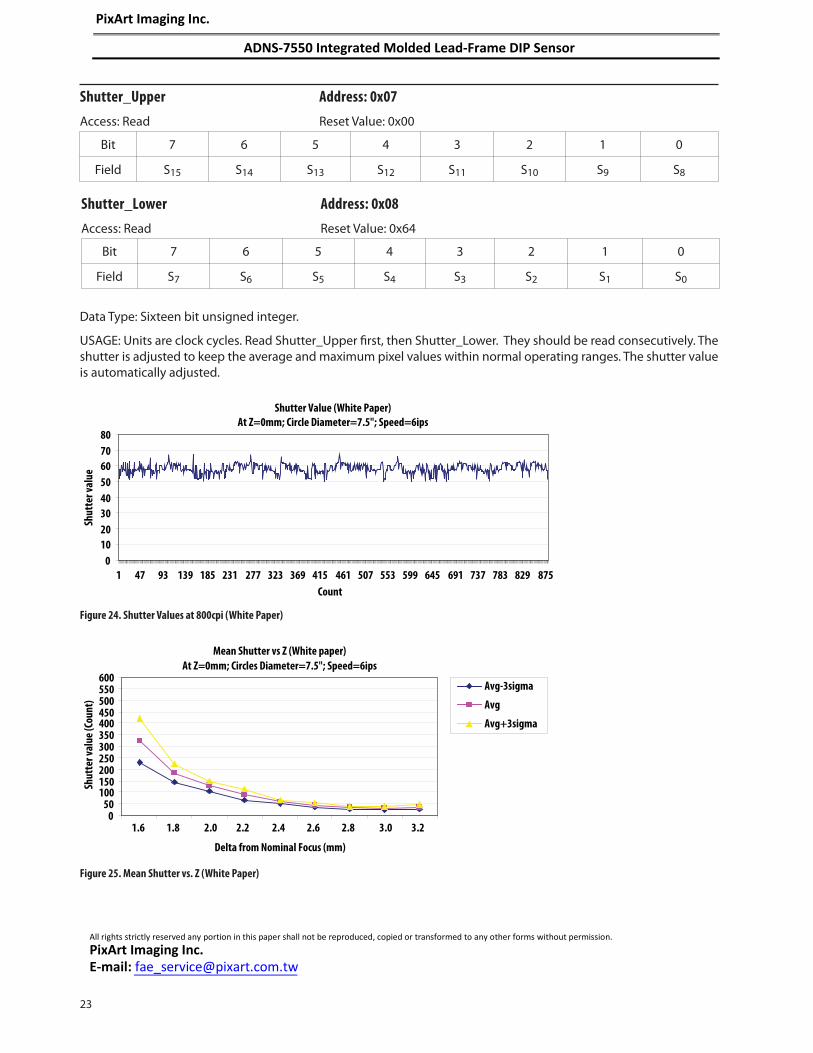
Shutter_Lower Address: 0x08
Access: Read Reset Value: 0x64
Shutter_Upper Address: 0x07
Access: Read Reset Value: 0x00
Data Type: Sixteen bit unsigned integer.
USAGE: Units are clock cycles. Read Shutter_Upper fi rst, then Shutter_Lower. They should be read consecutively. The shutter is adjusted to keep the average and maximum pixel values within normal operating ranges. The shutter value is automatically adjusted.
Bit 7 6 5 4 3 2 1 0
Field S7 S6 S5 S4 S3 S2 S1 S0
Bit 7 6 5 4 3 2 1 0
Field S15 S14 S13 S12 S11 S10 S9 S8
Figure 24. Shutter Values at 800cpi (White Paper)
Figure 25. Mean Shutter vs. Z (White Paper)
Shutter Value (White Paper)
At Z=0mm; Circle Diameter=7.5"; Speed=6ips
0
10
20
30
40
50
60
70
80
1 47 93 139 185 231 277 323 369 415 461 507 553 599 645 691 737 783 829 875
Count
Shu
tter
val
ue
Mean Shutter vs Z (White paper)
At Z=0mm; Circles Diameter=7.5"; Speed=6ips
050
100150200250300350400450500550600
1.6 1.8 2.0 2.2 2.4 2.6 2.8 3.0 3.2
Delta from Nominal Focus (mm)
Shu
tter
val
ue
(Cou
nt)
Avg-3sigma
Avg
Avg+3sigma
All rights strictly reserved any portion in this paper shall not be reproduced, copied or transformed to any other forms without permission.
PixArt Imaging Inc. E-mail: [email protected]
PixArt Imaging Inc.
ADNS-7550 Integrated Molded Lead-Frame DIP Sensor

24
Pixel_Sum Address: 0x0a
Access: Read Reset Value: 0x80
Data Type: High 8 bits of an unsigned 16-bit integer.
USAGE: This register is used to fi nd the average pixel value. It reports the upper eight bits of a 18-bit counter, which sums all pixels in the current frame. It may be described as the full sum divided by 1024. To fi nd the average pixel value, use the following formula:
Average Pixel = Register Value * 1024/676 = Register Value * 1.515
The maximum register value is 167. The minimum is 0. The pixel sum value can change on every frame.
Bit 7 6 5 4 3 2 1 0
Field AP7 AP6 AP5 AP4 AP3 AP2 AP1 AP0
Bit 7 6 5 4 3 2 1 0
Field MP7 MP6 MP5 MP4 MP3 MP2 MP1 MP0
Maximum_Pixel Address: 0x09
Access: Read Reset Value: 0xd0
Data Type: Eight-bit number.
USAGE: Maximum Pixel value in current frame. Minimum value = 0, maximum value = 254. The maximum pixel value can vary with every frame.
Minimum_Pixel Address: 0x0b
Access: Read Reset Value: 0x00
Data Type: Eight-bit number.
USAGE:Minimum Pixel value in current frame. Minimum value = 0, maximum value = 254. The minimum pixel value can vary with every frame.
Bit 7 6 5 4 3 2 1 0
Field MP7 MP6 MP5 MP4 MP3 MP2 MP1 MP0
All rights strictly reserved any portion in this paper shall not be reproduced, copied or transformed to any other forms without permission.
PixArt Imaging Inc. E-mail: [email protected]
PixArt Imaging Inc.
ADNS-7550 Integrated Molded Lead-Frame DIP Sensor

25
CRC0 Address: 0x0c
Access: Read Reset Value: 0x00
Data Type: Eight-bit number.
USAGE: Register 0x0c reports the fi rst byte of the system self test results. Value = F4.
Bit 7 6 5 4 3 2 1 0
Field CRC07 CRC06 CRC05 CRC04 CRC03 CRC02 CRC01 CRC00
CRC1 Address: 0x0d
Access: Read Reset Value: 0x00
Data Type: Eight-bit number.
USAGE: Register 0x0d reports the second byte of the system self test results. Value = 54.
Bit 7 6 5 4 3 2 1 0
Field CRC17 CRC16 CRC15 CRC14 CRC13 CRC12 CRC11 CRC10
CRC2 Address: 0x0e
Access: Read Reset Value: 0x00
Data Type: Eight-bit number.
USAGE: Register 0x0e reports the third byte of the system self test results. Value = 6D.
Bit 7 6 5 4 3 2 1 0
Field CRC27 CRC26 CRC25 CRC24 CRC23 CRC22 CRC21 CRC20
CRC3 Address: 0x0f
Access: Read Reset Value: 0x00
Data Type: Eight-bit number.
USAGE: Register 0x0f reports the fourth byte of the system self test results. Value = EB.
Bit 7 6 5 4 3 2 1 0
Field CRC37 CRC36 CRC35 CRC34 CRC33 CRC32 CRC31 CRC30
All rights strictly reserved any portion in this paper shall not be reproduced, copied or transformed to any other forms without permission.
PixArt Imaging Inc. E-mail: [email protected]
PixArt Imaging Inc.
ADNS-7550 Integrated Molded Lead-Frame DIP Sensor

26
Self_Test Address: 0x10
Access: Write Reset Value: NA
Data Type: Bit fi eld
USAGE: Before performing system self test, reset the chip. Then, set the TESTEN bit in register 0x10 to start the system self test. The test takes 250ms. During this time, do not write or read through the SPI port. Results are available in the CRC0-3 registers. After self-test, reset the chip again to start normal operation.
Bit 7 6 5 4 3 2 1 0
Field Reserved Reserved Reserved Reserved Reserved Reserved Reserved TESTEN
Field Name Description
TESTEN Enable System Self Test0 = Disabled1 = Enable
Reserved Address: 0x11
Confi guration2_bits Address: 0x12
Access: Read/Write Reset Value: 0x28
Data Type: Bit fi eld
USAGE: Register 0x12 allows the user to change the confi guration of the sensor. The RES bit allows selection between 400, 800, 1200 and 1600 cpi resolution.
Bit 7 6 5 4 3 2 1 0
Field 0 RES1 RES0 Reserved Reserved Reserved Reserved Reserved
Field Name Description
RES[1:0] Sets resolution 00 = 40001 = 80010 = 120011 = 1600
Reserved Address: 0x1b
All rights strictly reserved any portion in this paper shall not be reproduced, copied or transformed to any other forms without permission.
PixArt Imaging Inc. E-mail: [email protected]
PixArt Imaging Inc.
ADNS-7550 Integrated Molded Lead-Frame DIP Sensor

27
LASER_CTRL0 Address: 0x1a
Access: Read/Write Reset Value: 0x00
Data Type: Bit fi eld
USAGE: This register is used to control the laser drive. Bits 7 and 6 require complement values in register 0x1F. If the registers do not contain complementary values for these bits, the laser is turned off and the LP_VALID bit in the MOTION register is set to 0. The registers may be written in any order after the power ON reset.
Bit 7 6 5 4 3 2 1 0
Field Range1 Range0 Reserved Reserved CAL2 CAL1 CAL0 Force_Disable
Field Name Description
Range[1:0] Rbin Settings00= Laser current range from approximately 0.9mA to 3mA01= Laser current range from approximately 2mA to 5mA11 = Laser current range from approximately 4mA to 10mA10 = Invalid setting, LPVALID will be set and laser will off .
CAL2-0 Laser calibration mode - Write 101b to bits [3,2,1] to set the laser to continuous ON (CW) mode. - Write 000b to exit laser calibration mode, all other values are not recommended. Reading the Motion register (0x02 or 0x42) will reset the value to 000b and exit calibration mode.
Force_Disable LASER force disabled0 = LASER_NEN functions as normal1 = LASER_NEN output is high.
All rights strictly reserved any portion in this paper shall not be reproduced, copied or transformed to any other forms without permission.
PixArt Imaging Inc. E-mail: [email protected]
PixArt Imaging Inc.
ADNS-7550 Integrated Molded Lead-Frame DIP Sensor

28
LSRPWR_CFG0 Address: 0x1c
Access: Read/Write Reset Value: 0x00
Data Type: 8 Bit unsigned
USAGE: This register is used to set the laser current. It is to be used together with register 0x1D, where register 0x1D contains the complement of register 0x1C. If the registers do not contain complementary values, the laser is turned off and the LP_VALID bit in the MOTION register is set to 0. The registers may be written in any order after the power ON reset.
Bit 7 6 5 4 3 2 1 0
Field LP7 LP6 LP5 LP4 LP3 LP2 LP1 LP0
Field Name Description
LP7 – LP0 Controls the 8-bit DAC for adjusting laser current.One step is equivalent to (1/384)*100% = 0.26% drop of relative laser current.Refer to the table below for examples of relative laser current settings.
LP7 - LP3 LP 2 LP 1 LP 0 Relative Laser Current
00000 0 0 0 33.59%
00000 0 0 1 33.85%
00000 0 1 0 34.11%
: : : : : : :
11111 1 0 1 99.48%
11111 1 1 0 99.74%
11111 1 1 1 100%
LSRPWR_CFG1 Address: 0x1d
Access: Read/Write Reset Value: 0x00
Data Type: 8 Bit unsigned
USAGE: The value in this register must be a complement of register 0x1C for laser current to be as programmed, otherwise the laser is turned off and the LP_VALID bit in the MOTION register is set to 0. Registers 0x1C and 0x1D may be written in any order after power ON reset.
Bit 7 6 5 4 3 2 1 0
Field LPC7 LPC6 LPC5 LPC4 LPC3 LPC2 LPC1 LPC0
Reserved Address: 0x1e
All rights strictly reserved any portion in this paper shall not be reproduced, copied or transformed to any other forms without permission.
PixArt Imaging Inc. E-mail: [email protected]
PixArt Imaging Inc.
ADNS-7550 Integrated Molded Lead-Frame DIP Sensor

29
LASER_CTRL1 Address: 0x1f
Access: Read/Write Reset Value: 0x00
Data Type: 8 Bit unsigned
USAGE: Bits 7 and 6 of this register must be the complement of the corresponding bits in register 0x1A for the VCSEL control to be as programmed, otherwise the laser turned is off and the LP_VALID bit in the MOTION register is set to 0. Registers 0x1A and 0x1F may be written in any order after power ON reset.
Bit 7 6 5 4 3 2 1 0
Field Range_C1 Range_C0 Reserved Reserved Reserved Reserved Reserved Reserved
Reserved Address: 0x20-0x2d
Observation Address: 0x2e
Access: Read/Write Reset Value: 0x00
Data Type: Bit fi eld
USAGE: Register 0x2e provides bits that are set every frame. It can be used during EFT/B testing to check that the chip is running correctly. Writing anything to this register will clear the bits. Wait for at least one frame before reading the register.
Bit 7 6 5 4 3 2 1 0
Field Reserved Reserved Reserved OBS4 OBS3 OBS2 OBS1 OBS0
Field Name Description
OBS4-0 Set every frame
Reserved Address: 0x2f-0x34, 0x36-0x39
All rights strictly reserved any portion in this paper shall not be reproduced, copied or transformed to any other forms without permission.
PixArt Imaging Inc. E-mail: [email protected]
PixArt Imaging Inc.
ADNS-7550 Integrated Molded Lead-Frame DIP Sensor

30
Pixel_Grab Address: 0x35
Access: Read/Write Reset Value: 0x00
Data Type: 8 Bit Word
USAGE: For test purposes, the sensor will read out the contents of the pixel array, one pixel per frame. To start a pixel grab, write anything to this register to reset the pointer to pixel 0,0. Then read the PIXRDY bit in the Motion register. When the PIXRDY bit is set, there is valid data in this register to read out. After the data in this register is read, the pointer will automatically increment to the next pixel. Reading may continue indefi nitely; once a complete frame’s worth of pixels has been read, PIXFIRST will be set to high to indicate the start of the fi rst pixel and the address pointer will start at the beginning location again.
Bit 7 6 5 4 3 2 1 0
Field PD7 PD6 PD5 PD4 PD3 PD2 PD1 PD0
Top X-ray View of Mouse
RBLB
POSITIVE
Y
POSITIVE X
1
2
3
4
5
6
7
8
16
15
14
13
12
11
10
9
Figure 26. Pixel Address Map (sensor looking on the navigation surface through the lens)
All rights strictly reserved any portion in this paper shall not be reproduced, copied or transformed to any other forms without permission.
PixArt Imaging Inc. E-mail: [email protected]
PixArt Imaging Inc.
ADNS-7550 Integrated Molded Lead-Frame DIP Sensor
31
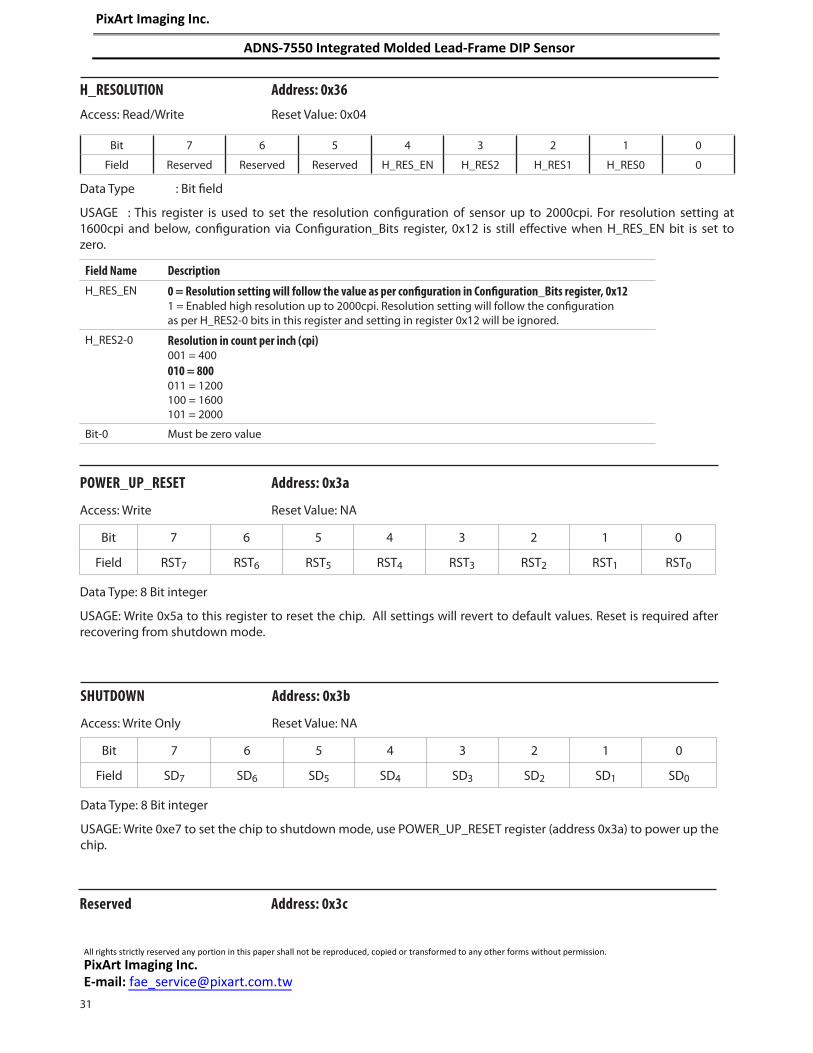
SHUTDOWN Address: 0x3b
Access: Write Only Reset Value: NA
Data Type: 8 Bit integer
USAGE: Write 0xe7 to set the chip to shutdown mode, use POWER_UP_RESET register (address 0x3a) to power up the chip.
Bit 7 6 5 4 3 2 1 0
Field SD7 SD6 SD5 SD4 SD3 SD2 SD1 SD0
Reserved Address: 0x3c
POWER_UP_RESET Address: 0x3a
Access: Write Reset Value: NA
Data Type: 8 Bit integer
USAGE: Write 0x5a to this register to reset the chip. All settings will revert to default values. Reset is required after recovering from shutdown mode.
Bit 7 6 5 4 3 2 1 0
Field RST7 RST6 RST5 RST4 RST3 RST2 RST1 RST0
H_RESOLUTION Address: 0x36
Access: Read/Write Reset Value: 0x04
Bit 7 6 5 4 3 2 1 0
Field Reserved Reserved Reserved H_RES_EN H_RES2 H_RES1 H_RES0 0
Data Type : Bit fi eld
USAGE : This register is used to set the resolution confi guration of sensor up to 2000cpi. For resolution setting at 1600cpi and below, confi guration via Confi guration_Bits register, 0x12 is still eff ective when H_RES_EN bit is set to zero.
Field Name Description
H_RES_EN 0 = Resolution setting will follow the value as per confi guration in Confi guration_Bits register, 0x121 = Enabled high resolution up to 2000cpi. Resolution setting will follow the confi gurationas per H_RES2-0 bits in this register and setting in register 0x12 will be ignored.
H_RES2-0 Resolution in count per inch (cpi)001 = 400010 = 800011 = 1200100 = 1600101 = 2000
Bit-0 Must be zero value
All rights strictly reserved any portion in this paper shall not be reproduced, copied or transformed to any other forms without permission.
PixArt Imaging Inc. E-mail: [email protected]
PixArt Imaging Inc.
ADNS-7550 Integrated Molded Lead-Frame DIP Sensor

Motion_Burst Address: 0x42
Access: Read Reset Value: 0x00
Data Type: Various
USAGE: Read from this register to activate burst mode. The sensor will return the data in the Motion register, Delta_X_L, Delta_Y_L, Delta_XY_H, Squal, Shutter_Upper, Shutter_Lower and Maximum_Pixel. Reading the fi rst 3 bytes clears the motion data. The read may be terminated anytime after Delta_X is read.
Bit 7 6 5 4 3 2 1 0
Field MB7 MB6 MB5 MB4 MB3 MB2 MB1 MB0
Inverse_Revision_ID Address: 0x3e
Access: Read Reset Value: 0xfc
Data Type: Inverse 8-Bit unsigned integer
USAGE: This value is the inverse of the Revision_ID. It can be used to test the SPI port.
Bit 7 6 5 4 3 2 1 0
Field NRID7 NRID6 NRID5 NRID4 NRID3 NRID2 NRID1 NRID0
Inverse_Product_ID Address: 0x3f
Access: Write Only Reset Value: 0xcd
Data Type: Inverse 8-Bit unsigned integer
USAGE: This value is the inverse of the Product_ID. It can be used to test the SPI port.
Bit 7 6 5 4 3 2 1 0
Field NPID7 NPID6 NPID5 NPID4 NPID3 NPID2 NPID1 NPID0
Shut_thr Address: 0x3d
Access: Read/Write Reset Value: 0x56
Data Type: 7 Bit number
USAGE: Threshold defi nes the Shutter value when lifted runaway happens.
Sensor will suspect lifted runaway happens and suppress motion if (Shutter > Shut_thr[7:1]*32).
Bit 7 6 5 4 3 2 1 0
Field Shut_thr7 Shut_thr6 Shut_thr5 Shut_thr4 Shut_thr3 Shut_thr2 Shut_thr1 Reserved
All rights strictly reserved any portion in this paper shall not be reproduced, copied or transformed to any other forms without permission.
PixArt Imaging Inc. E-mail: [email protected]
PixArt Imaging Inc.
ADNS-7550 Integrated Molded Lead-Frame DIP Sensor
Related Documents