AUXILIARY ENGINE DIGITAL INTERFACE UNIT (DIU) CONTRACT NO. NAS8-27323 FINAL REPORT AUGUST1972 I "pEFA^Mif >„*""»" ip GI »S DIGITAL : (.l-ctronic Co-.L^J"^ »JP«t juq _ CSCL 09C ELECTRONIC A SUBSIDIARY OF NCR G3/10 N72-33231 Dnclas 16412 16^112 COMMUNICATIOIMS SYSTEM DEVELOPMENT COMMUNICATIONS DATA LINK DATA PROCESSING ANTENNAS MULTIPLEXERS ST. PETERSBURG, FLORIDA https://ntrs.nasa.gov/search.jsp?R=19720025581 2020-05-16T16:19:07+00:00Z

Welcome message from author
This document is posted to help you gain knowledge. Please leave a comment to let me know what you think about it! Share it to your friends and learn new things together.
Transcript
AUXILIARY ENGINE DIGITAL INTERFACE
UNIT (DIU)
CONTRACT NO. NAS8-27323
FINAL REPORT
AUGUST 1972
I "pEFA^Mif >„*""»" ipGI»S DIGITAL: (.l-ctronic Co-.L^J"^ »JP«t j u q _
CSCL 09C
ELECTRONICA SUBSIDIARY OF NCR
G3/10
N72-33231
Dnclas1641216^112
COMMUNICATIOIMS
SYSTEM DEVELOPMENT
COMMUNICATIONS
DATA LINK
DATA PROCESSING
ANTENNAS
MULTIPLEXERS
ST. PETERSBURG, FLORIDA
https://ntrs.nasa.gov/search.jsp?R=19720025581 2020-05-16T16:19:07+00:00Z
AUXILIARY ENGINE DIGITAL INTERFACE
UNIT (DIU)
CONTRACT NO. NAS8-27323
Prepared for
NATIONAL AERONAUTICS AND SPACE ADMINISTRATIONGEORGE Co MARSHALL SPACE FLIGHT CENTER
HUNTSVILLE, ALABAMA 35812
FINAL REPORT
AUGUST 1972 ,
ELECTRONICCOMMUNICATIONS, INC.Box 12248 (1501 72° St. N.J
St. Petersburg, Florida 33733
TABLE OF CONTENTS
Paragraph Title Page
1.0 Introduction 1
2.0 Design Philosophy 2
3. 0 Auxiliary Propulsion Engine DigitalInterface Unit Electrical Design 2
3.1 Summary of Electrical Design 2
3.1.1 Functional Complexities 2
3.1. 2 Performance of CMOS Logic 4
3.2 Systems Functional Description 5
3. 201 Input Data Validity Comparison 5
3.2.2 Firing Logic 7
3. 20 3 Spark and Valve Drivers 9
3. 2.4 High Voltage Supply 9
3. 2. 5 Emergency Shutoff Monitor 9
3.2.6 Strain Gauge Amplifiers 10
3. 2.7 Pressure Threshold Detectors and A/D Converters 10
3. 2, 8 Status Monitor 11
3.2.9 Test Sequencer 11
3. 3 Module Designs 14
3.3.1 Supervisory Parity Checker; Board No. 2-~ 14
3.3.2 Single Bit Majority Voter; Board No. 3 17
3. 3. 3 Serial Voter; Board No. 4 17
3. 3.4 Supervisory Serial and Storage Registers; Boards 6 & 7 20
3. 3. 5 One's Decoder; Board No. 8 22
3. 3. 6 Zero's Decoder; Board No. 9 22
3o 30 7 Status Monitor Multiplexer; Board No. 13 22
3. 3. 8 Status Monitor Parity Generator and ShiftRegister; Board No. 14 22
TABLE OF CONTENTS
Paragraph,. •• Title Page
3. 3. 9 Polar RZ Modulator) Board,No. 16- - - 27
3.3.10 Line Receiver-Photo Isolator InterfaceCircuit; Board No,. 18- ' 27
3. 3.11; System Clock Generator;'Board No. 19 30
3.3.12 (Dual) Tracking Analo'g-to-Digital Converter;Board No. 20--- .-. 30
30 3. 13 Emergency Shutoff Monitor; Board No, 21 33
3,, 3.14 Emergency Shutoff Monitor; Board No, 22 33
3. 30 15* Power Enable/Disable Module; Types "A","B" and "C"; Board No. 23 '36
3.3.15.1 Board Type'"A"- '-' 36
3. 3.15. 2 Board Type "B"- -"- - - -'- 41
3.3.15.3 " Board'Type "C" 41
3. 3,16 Function Monitor; Board No. 24 43
3.3.17 Firing Logic; Board No. 25 43
3. 3.18 Chamber Pressure Amplifier/Comparatorand A/D Converter; Board No. 26- - 48
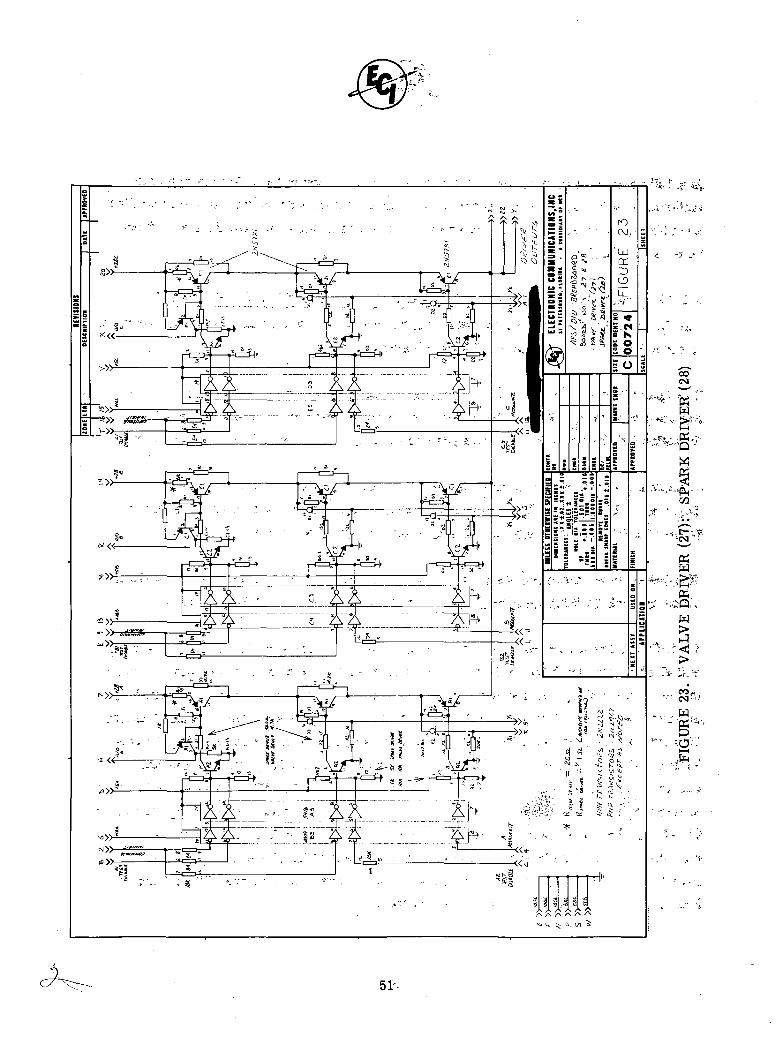
3. 3oi9 Spark Driver; Board No. 27;Valve Driver; Board No. 28 50
3.3.20 Line Pressure Amplifier/Comparator;< Board No; 30-- - _ _ - v _ 52
3.3.21 A/D Clocks; Board No, 31- 52
3. 3. 22 < Status Monitor Timing and Control; Board No. 32 52
3.3.23 Subroutine Word Test Read Logic; Board No. 33 58
3.3.24 Test Sequencer Control Memory; Board No. 34 58
3 0 3.25 V " - Test Sequencer Timing and Control Logic;Board No. 35 -r 63
* " . . • > - •
3. 3. 26., , Subroutine Control Logic; Board No. 36 65
3. 3. 27 Firing Logic; Valve and Spark Driver TestEncoder; Board No. 37 69
11
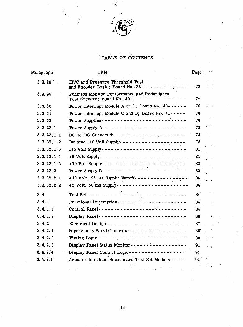
TABLE OF C'ONTENTS
Paragraph Title Page
3.3.28 ISVC and Pressure Threshold Testand Encoder Logic;- Board No. • 3.8 : - 72
3.3.29 Function Monitor Performance and RedundancyTest Encoder; Board No. 39- 74
3. 3. 30 Power Interrupt Module A or B; Board No. 40- 76
3. 3. 31 Power Interrupt Module C and D; Board No. 41 78
3. 3. 32 Power Supplies --• •• 78
3. 3. 32.1 Power Supply A - - - •>'' ' 783. 3. 32.1.1 DC-to-DC Converter r _ _ - _ _ 73
3.3.32.1.2 Isolated ±10 Volt Supply 73
3. 3. 32.1.3 ±15 Volt Supply- - - 81
3.3.32.1.4 +5 Volt Supply ' - - - - 81
3.3.32.1.5 +10 Volt Supply --.-' - : - - 82
3. 3. 32. 2 Power Supply D 82
3. 3. 32. 2.1 +10 Volt, 25 ma Supply Shutoff , 84
3. 3. 32. 2. 2 +5 Volt, 50 ma Supply 84
3.4 Test Set 84'f
3.4. 1 Functional Description- -,-- ; - - 84
3.4.1,1 Control Panel .--'-. 84
3.4.1. 2 Display Panel . 86
3.4.2. Electrical Design -,---- 87
3.4. 2. 1 Supervisory Word Generator- - - 883.4.2.2 Timing Logic - - - - - - - - ~ ._ 88
3.4. 2. 3 Display Panel Status Monitor- 91
3.4.2.4 Display Panel Control Logic 91
3.4. 2. 5 Actuator Interface Breadboard Test Set Modules 95
111
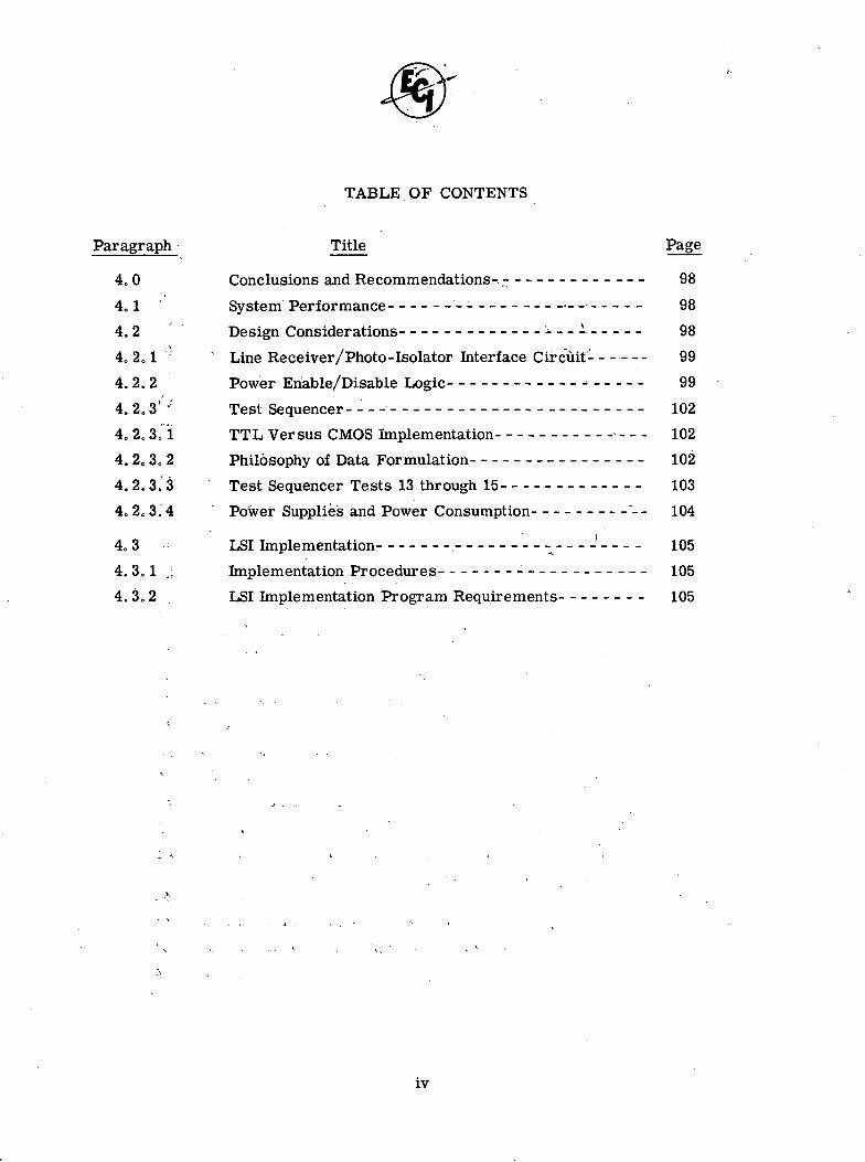
TABLE OF CONTENTS
Paragraph Title
4.0 Conclusions and Recommendations- 98
401 ' System Performance _ _ _ _ 98
4.2 Design Considerations '- - - -> 98
40 201 Line Receiver/Photo-Isolator Interface Circuit- 99
4.2.2 Power Enable/Disable Logic 99
4.2.3' ' Test Sequencer---- 102
4,, 2.3,1 TTL Versus CMOS Implementation- 102
4. 20 3, 2 Philosophy of Data Formulation 102
4.2.3.3 Test Sequencer Tests 13 through 15 103
40 2o 3.4 " Power Supplies and Power Consumption "-- 104
4, 3 - LSI Implementation . -^ ' 105
4. 3,1. ; Implementation Procedures • 105
4. 30 2 LSI Implementation Program Requirements 105
IV
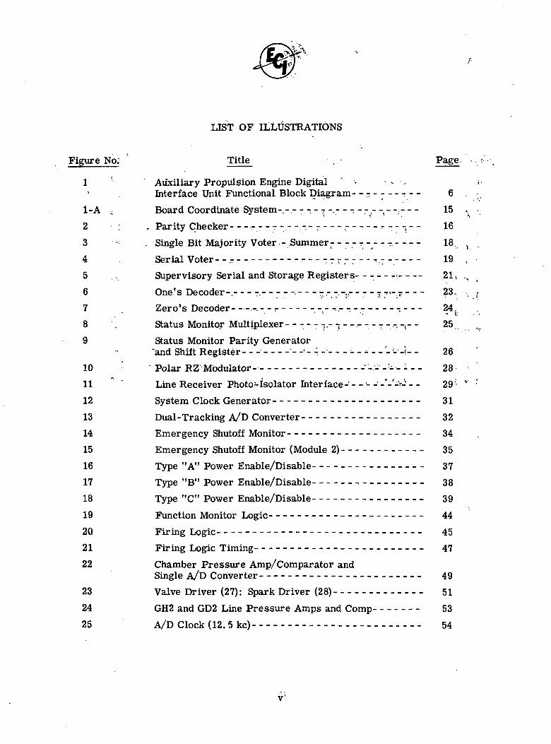
LIST OF ILLUSTRATIONS
Figure No; Title
1 ! Auxiliary Propulsion Engine Digital ' - - ;Interface Unit Functional Block Diagram- - - r-- 6 ,
1-A . Board Coordinate System-.-.--^.-T------rr~,--; 15 •> -.2 ; , Parity Checker - - - - - - - , - - 7 • r-"-- I6
3 - . Single Bit Majority Voter - .Summerr - - - r - - - -.- - - - 18 ^ ,
4 Serial Voter- - - - - - - ? r - - - - - - - - 19 ,
5 Supervisory Serial and Storage Registers------' 21s .,
6 One's Decoder-. -. ,-.-.-r - - - - ---,- 23.. ,.7 Zero's Decoder . _ - - - - - - _ _ _ _ _ _ _ 24,
• • ' - • - . - . 5 ; . .
8 , Status Monitor Multiplexer . - - - - - ( - - - - - - - - - > , - - 251 ,v9 Status Monitor Parity Generator
'and Shift Register - - _ • - - _ ^ _ _ _ - _ • _ _ " ; _ _ 26
10 Polar RZ Modulator- - ---- '-- 1 - - 28 •
11 Line Receiver Photo-Isolator Interface------"-'- r--- 29'- *' r
12 System Clock Generator 31
13 Dual-Tracking A/D Converter 32
14 Emergency Shutoff Monitor 34
15 Emergency Shutoff Monitor (Module 2) 35
16 Type "A" Power Enable/Disable 37
17 Type "B" Power Enable/Disable 38
18 Type "C" Power Enable/Disable 39
19 Function Monitor Logic 44
2Q Firing Logic 45
21 Firing Logic Timing 47
22 Chamber Pressure Amp/Comparator andSingle A/D Converter 49
23 Valve Driver (27): Spark Driver (28) -- -- 51
24 GH2 and GD2 Line Pressure Amps and Comp 53
25 A/D Clock (12. 5 kc) -- 54
v'

LIST OF ILLUSTRATIONS
Figure No. Title Pago
26 Status Monitor Timing and Control- 56
27 Status Monitor Timing Diagram- - - - 57
28 Subroutine Word Test Read Logic 59
29 Test Sequencer Control Memory 60
30 Test Sequencer Timing and Control 64
31 " Subroutine Logic 66
32 Subroutine Timing and Control 68
33 Firing Logic Valve and Spark Driver, Test Encoder- 70
34 ISVC Test Encoder and Pressure ThresholdTest Encoder 73
35 Function Monitor Redundancy and PerformanceTest Encoder 75
36 Power Interrupt Circuits A & B - - 77
37 Power Interrupt Circuits C&D 79
38 Power Supply "A" "B" or "C" 80
39 Power Supply "D" 83
40 Actuator Interface Unit Test Set 85
41 Supervisory Word Generator and Control 89
42 Timing Logic 90
43 Timing and Control 92
44 Display Panel Status Monitor 93
45 Display Panel Control Logic 94
46 Clock Generator and A/D Converter : - 96
47 AI Data Generator 97
48 Polar RZ Line Receiver Interface 100
49 Substitute Power Enable/Disable Driver 101
50 LSI Prototype Process Flow Diagram 106
VI
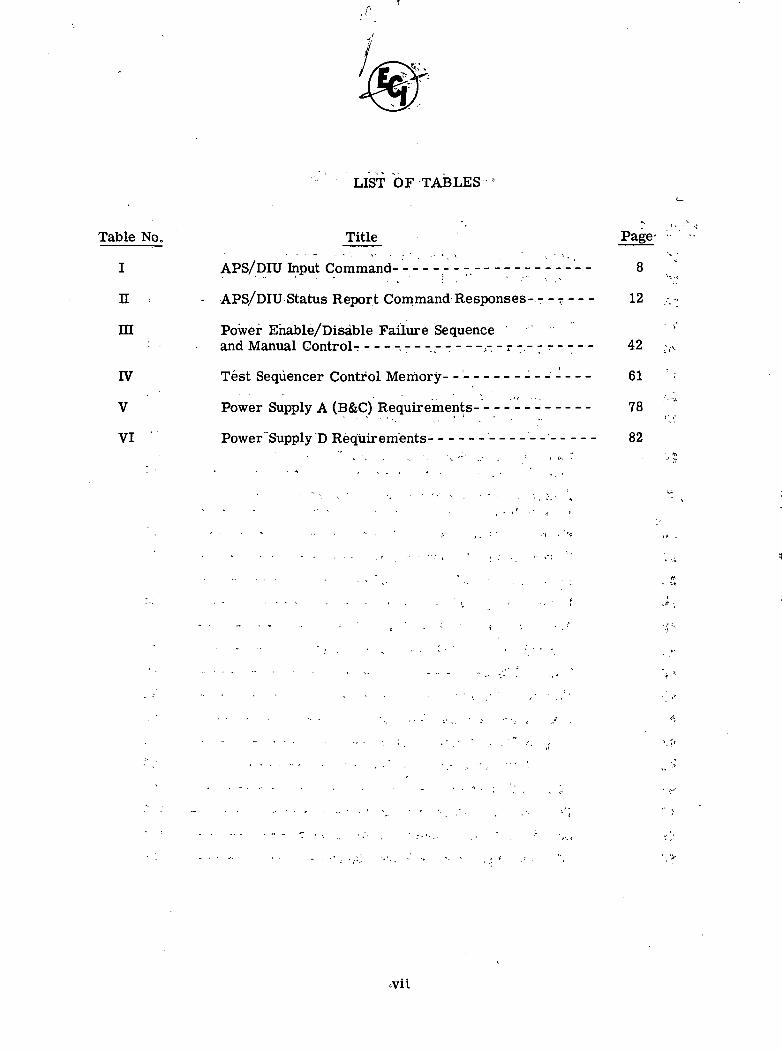
LIST OF TABLES
• **
Table No. Title Page-
I APS/DIU Input Command--- - - - - 7. 8 '
n • APS/DIU Status Report Command Responses---7 12
HI Power Enable/Disable Failure Sequenceand Manual Control T • - - - . - - > - . - T - . - - - - - - - 42
IV Test Sequencer Control Memory- 61 ;
V Power Supply A (B&C) Requirements 78
VI Power Supply D Requirements- _ _ _ _ 82
AUXILIARY PROPULSION SYSTEM/DIGITAL INTERFACE UNIT
(APS/DIU) BREADBOARD
FINAL REPORT
1.0 INTRODUCTION
On April 27, 1971, ECI was contracted to design, fabricate and test an Auxiliary Propul-
sion Engine Digital Interface Unit oriented for application on the Space Shuttle. Thisunit controls both the valving of the fuel and oxidizer to the engine combustion chamber
and the ignition spark required for timely and efficient engine burns.
In addition to this basic function, the unit is designed to manage it's own redundancy
such that it is still operational after two hard circuit failures. Further, it communi-cates to the data bus system several selected information points relating to the opera-
tional status of the electronics as well as the engine fuel and burning processes.
The system design represents a significant advance in the state-of-the-art of digitali
systems for NASA in that it proves out the feasibility of implementing ComplimentaryMOS circuitry both in discrete form or LSI form within the Shuttle vehicle control
systems. In addition, this implementation typically demonstrates the level of complexityrequired to acquire subsystem dual-failure immunity.
2. 0 DESIGN PHILOSOPHY
The underlying philosophy behind the circuits designed for the APS/DIU is that theyeasily be implemented into CMOS LSI with a minimum of documentation alterations.Several breadboard modules, in this case, could be incorporated within a single LSI
chip where the two prime considerations are device density and I/O requirements.
This philosophy creates complexity in a breadboard system that would not otherwise be
required if the system were merely constructed with discrete logic or passive\
components. For example, a seven input NAND function is a simple part within a LSI
chip and the addition of three inputs to a four input NAND layout occupies very little
real estate. However, a seven input gate was not available in CMOS during the
fabrication of this breadboard and had,to be constructed from several devices. This
occupies.-quite a bit .of breadboard real estate and is costly in that the excess gates
within, the packages required to create the function are not always useful at the given
location.
To minimize this costly approach, the breadboard was fabricated of pure CMOS where
timing and propogation considerations were of a critical nature. Here, the function
may be transferred directly to a LSI configuration with little or no logic alterations,,
An example of these designs are found in the Input Supervisory Validity Comparison and
Status Monitor Circuits.
Alternately, where timing and propogation delays are not considered critical, discrete
components are used to compliment the use ofv additional logic thereby reducing com-
plexities and cost. Several examples of this will be demonstrated in this report.
Functionally, the designs with discrete components perform identically to the pure
logic form desired. ;
3. 0 AUXILARY PROPULSION ENGINE DIGITAL INTERFACE UNIT ELECTRICAL
DESIGN
3.1 SUMMARY OF ELECTRICAL DESIGN
The purpose of this breadboard has been to:
(1) verify the feasibility and operational complexity of an APS/Dilicapable of dual-failure immunity
' (2) verify the feasibility and performance parameters of Complimentary• , - f . . - , MOS. logic in performing this function.
3.1.1 Functional Complexities . .
To complete these tasks, the circuits were fabricated using CMOS on plug-in cards
which were rack-partitioned within a commercial bench style cabinet. The circuits
were partitioned both according to module function as well as a redundant function. Here,
inter changeability is maintained as universal as possible for performance evaluation ;. •
and troubleshooting. Where simplicity dictated that'a specific function and it's re- • -> :
dundant'couhterparts should be mounted on the same module, it was done so. Here,'" ' •
testing and observation can be accomplished by placing the card on an extender card. '
Each module is powered in accordance with the partitioning of the redundancy scheme.
That is, ftir example, Line Receiver "A" in position "A" is powered by:"A" power; supply.
It would be, however, capable of performing in the Lme Receiver "B" position in which
case it would become Line Receiver "B", Exceptions to this arrangement are found on.
certain modules where single-failure majority voting is accomplished. Here, the:
power supplies are "ORed" to preempt a prime power failure reducing the majority
voting capability.
The module back plane wiring uses a point-to-point scramble scheme intended to reduce
cross-coupling capacity between signal paths. The power wiring is the only shielded - •< •
wiring in the system and the shields are intended to reduce the coupling'from the ' • •'•• '
current-carrying lines to the high-impedance signal lines. Because the system is«a ; :
breadboard by definition, no attempt to create cables was made since their formation
would, in most probability, be detrimental to the system performance'. '
The architecture of the system breadboard is, at best, a very poor representation of
an LSI type construction. The signal paths, for instance, are measured an feet instead-
of mils as would be the case on a chip. Nevertheless,, if the devices perform the , . ,
functions desired within this architecture, obviously the design would operate in an
LSI configuration. A computer verification of the shorter propogation delays in the
LSIlayout is all that is required to confirm nominal .operation.. In additipn,, the bread-
board architecture offers a circuit exposure to radiant noise that most certainly would
not exist in the LSI format. Again, the natural immunity of the circuit designs to noise
problems is demonstrated and assured to improve in the conversion to LSI. . ,-
The philosophy of dual-failure immunity would include.not only active device redundancy
but signal path redundancy to protect against.such failures as broken wires or failed .
connectors: •' The breadboard does not include the, signal path redundancies. The
thinking here was that the signal path wiring redundancy would do nothing to verify
the functional redundancies of the logic and would merely complicate the logic boards
and back-plane system. "And; the multitude of additional redundant wiring would not
necessarily be representative of the signal paths within an LSI system due to the
partitioning of the breadboard. Broken wires, failed solder or wirewrap connections
or interrupted connector connections should be relatively easy to locate and repair
within the breadboard'should they occur. .-; . •
3.1.2 Performance of CMOS Logic
Within the architecture discussed, the CMOS logic devices selected performed well
beyond ECI's expectations. Because they are very high impedance devices, we had
expected to witness rather severe noise pickup from sources different from the APS/DIU
as well as internal crosstalk and interference. This did not happen, in spite of the fact
that virtually all of the signal lines within the breadboard are excessive in length. The
system frequency limit is just about two megahertz because some pulse shape deterio-
ration was witnessed at these frequencies. This deterioration, however, was not
severe enough to inhibit the desired performance.
Perhaps the most severe problem that has existed in the application of CMOS,was the
difficulty in turning it off. Because of the input protective diode network, the logic will
perform it's natural function with the presence of an input signal. Here, the input
signal will provide power for the logic Vcc while not deteriorating the quality of the
signal pulse characteristics. Now, to test a specific logic function where several
similar functions are in parallel to provide the redundancy, the obvious method would
be to power down .the logic functions in sets and verify that the remaining sets still
perform as expected. Disconnecting power does not work in this case. Instead, the
input circuits had to be resistively isolated and the power lines of the specific function
pulled to ground. The resistive isolation was such that it did not load the desired inputs
to the active redundant circuits. .
An alternate method that resultantly was not ideal for the breadboard,, was to open the r *
signal inputs with logic switches. Here, each input (signal/ clock, etc.) would have to.-,,
have a series switch to interrupt signal and a parallel switch to commit the opened .
input. This method, although feasible, is not practical. The switches increase cost
complexity plus add a series element subject to failure.; . , : - • • • • • . •
Re-evaluation of this method .will be conducted, however, for an LSI fabrication to ;
assess its impact on reliability and cost. On a LSI chip, only the inputs would neces-
sarity have this network whereas on the breadboard every input-per-package is
protected. , - . - > - .... .. , ; ,<
3.2 SYSTEMS FUNCTIONAL DESCRIPTION
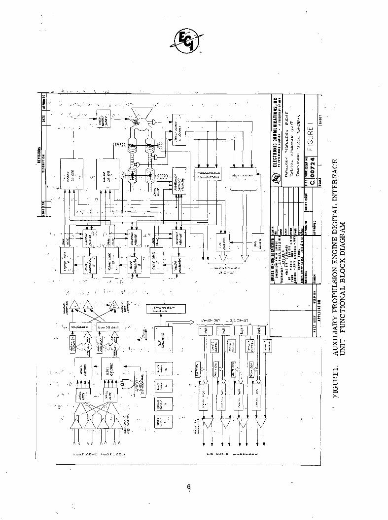
This section describes the operation of the APS/DIU as depicted in the Functional
Block Diagramj Figure 1 . , • • • • - . . • - . • . . ; . ' , . - . • „ • / ; , , • : ,
The data inputs to the APS/DIU from a Data Terminal which communicates with the
vehicle data bus/ The format of this information is 20 bits Polar RZ with the 2Qth bit
missing for word synchronization. The frequency is 1 MHz or 1 //sec/bit. , - . .;
3.2.1 Input Data Validity Comparison . = . . . . . /
The input line receivers accept this data from four separate but identical Data Terminals,
The "ones" and "zeros" are separated at the input to each line receiver and a set of : J
photo-isolators are fed separately. The secondary of the line receivers recovers this
isolated data and feeds corresponding serial voters! Here, the 1's (or O's)'are com- "'•
bined bit-by-bit in a Serial Voter to eliminate any two faulted lines and output the "
correct data on all four lines to four registers. As shown in the figure, both the 1's
and O's are processed into storage separately. The detected "end-of-word" is used to
load each new word. "• • ' ' : < J
From parallel storage, then, the information is parity checked and decoded and feeds "'• '
the Majority Voter Summers, one for each command. There is one Majority Voter
s o" O
~ o
LL!cr
LL
s: s
si
Wo<Cu-tewH
H
ra CQ
w
Summer for eac bit and it is this circuit which combines all eight sets of information _,
about a single command and outputs the correct state to a single redundant line. This -;
feature eliminates any contradictions of redundant command paths and insures that any ,
given command is sourced from a (virtual) single source. Table I lists the specific •'
commands for the APS/DIU and their encoded format. ,
3.2.2 Firing Logic ,
The firing logic sections are configured in triplicate such that a failure in "A" auto-
matically causes switchover to "B" and a failure in "B" causes automatic switchover to
"C. " The Firing Logic that is in use is the only one that is powered "on. " The others
are powered down until activated either automatically or by external commando -'
The system initiates itself into Firing Logic "A" at "power-on;" And, it will remain
there until it fails. < K its failure mode is such that it cannot (or itSfassociated drivers
cannot) operate the valve, then the switchover will occur the* first time an "engine-on"
command is issued. If its failure mode is such that it attempts to issue an uncommanded
"engine-on", then the switchover occurs immediately., Similarly, if "B" has an inert
failure as described.for "A", switchover to "C" will occur at the next "engine-on"
command. Switchover is again immediate for an uncommanded engine burn.J ?' *
A failure in Firing Logic "C" causes shutdown of the system until it is re-activated
either by external command or the power is re-cycled- The system does not attempt
to re-use a Firing Logic set that has previously been declared as failed.
The block diagram illustrates how each Firing Logic function is controlled by a Power
Enable/Disable and a Function Monitor. The Function Monitor examines the states of
the chamber pressure, input command, valve switches and valve and spark outputs
from Firing Logic and determines whether, the Firing Logic or its associated drivers
are outputting according to'command. When they do not, the Power Enable/Disable
function powers down the faulted logic and causes "turn-on" of the next back-up.

COMMAND NO. FUNCTION CODE
1 •• •' '•2"'" • ' • ' • ' -
•,.•:•: 3 .
4
5
6 ':
••• 7 •' ''•
' 8 ' * • • • ' :•'. 9 :• . •';
' 10' •
11' ' "';' 12 ' -'
13 • ' • ' ' •
14
15
16
17 -18
19
20
21
22
23
24
25
26
27
28
29
Inhibit Firing Logics B & C (use A)Inhibit Firing Logics A & C (use B)
' • Inhibit- Firing Logics A & B (use C) ,Inhibit Chamber Pressure Ampl AInhibit Chamber Pressure Ampl B
' ' ••' Inhibit' Chamber Pressure Ampl C• Inhibit GH2 Pressure Ampl A
Inhibit GH2 Pressure Ampl B
• '• ' inhibit GH2 Pressure Ampl C:" ' ' 'Inhibit GO2 Pressure Ampl A
' • ' • ' • ' • Inhibit GO2 Pressure Ampl B1 'Inhibit GO2' Pressure Ampl C• ••" ' '! '•• (SPARE) -
(SPARE)Status: Pressure Threshold; Chamb, GO2, GH2
Reset Override Commands. ;- Emergency Shutoff Command
Engine< Turn-OnEngine Turn -OffExercise "SELF-TEST" Program
Status: Valve Driver A & B CurrentStatus: Valve Driver C; Spark Driver A CurrentStatus: Spark Driver B, Spark Driver C CurrentStatus: GO2 Pressure Monitor 1 & 2Status: GH2 Pressure Monitor 1 & 2Status: GO2, GH2 Pressure Monitor 3Status: Chamber Pressure :Monitor 1 & 2Status: Chamb Pressure 3; Firing Logics; Function
MonitorsStatus: Spark Drivers; Valve Drivers; Valve Switches
00001000100001100100
00101
0011000111
0100001001
01010
01011
01100
01101.
01110
01111
10000
10001
10010
10011
10100
10101
10110
10111
11000
11010
11010
11011
11100
11101
TABLE L APS/DIU INPUT COMMANDS
8.
3.2.3 Spark and Valve Drivers
Each Firing Logic set feeds two drivers, one for valve and one for spark. Each .. , •.
driver contains a "modulate" stage plus two stage of series inhibit to disable the .
driver in the event of two shorting failures. The three drivers within, for, example,
the Valve Driver are in parallel but operate singly with a given Firing Logic set. .This
is true also for the Spark Driver. . ;
Both drivers are identical in structure and components with exception to the current-
measuring resistors which restrict the Valve Driver to 50 ma output while the Spark
Driver output is 1 ampere. This was intentionally done for this breadboard to demon-
strate the versatility of the circuit and to provide for loads which were undefined during
this program. It was assumed, therefore, that the valve would require 50 ma and the
current-monitoring resistors would swing 0 to 1 volt for this load. Similarly, the ;
spark was assumed to be 1 amp and the current monitor would also indicate 0 to 1,volt. .
These currents are continually monitored by A/D converters and can be accessed.at i
any time for information reporting to the data bus system. '. ..
3.2.4 High Voltage Supply , . ;
The High Voltage Supply illustrated in the block diagram is for information purposes -
only in describing the system and is not part of the APS/DIU. /This supply provides
spark for the engine combustion chamber. . • « • .
3 o 2 o 5 Emergency Shutoff Monitor • ' • •
The function of this device is to close the additional valve shown in the event of a j
catastrophic failure not self-correctable by the APS/DIU. The monitor compares the •
chamber and line pressure thresholds, the spark and valve outputs from the drivers:and the state of the valve switches. If there is an engine burn or a drop in pressures • ' :. ' . : Vindicating that the line valves are, in fact, open without being driven open the Emergency
.Shutoff Valves are closed.
9
It should be noted that the.Emergency Shutoff Monitor performs differently from the
Function. Monitors. The ESO Monitor seeks uncommanded and undriven enginereactions. The Function Monitors seeks faulty commands which were not dictated to
the APS/DIU0 The ESO monitor may cause shutdown of the Firing Logics depending
on the conditions but the Function,Monitors will never cause Emergency shutoff.
3.2.6 Strain Gauge Amplifiers , :. , . ,
These amplifiers are analog interfaces with the pressure transducers located in the
GH2 and GO2 fuel lines plus the engine combustion chamber. The original intent of thesystem design was that these amplifiers interface with redundant strain gauge pressuretransducers.. However, for purposes of this breadboard, at least, the triplex sets
interface, with a single transducer for each of the monitoring points. The breadboard
is configured such that either configuration may be employed with minimum adjustmentto the circuitry., ,.In addition,; each amplifier set is presently oriented to interface with
a single strain.gauge with the bridges configured on the breadboard. Alternate typesof pressure transducers may be substituted by eliminating the bridge circuitry and re-
scaling the amplifiers.
It is the function of these amplifiers to monitor the specific pressures at their designatedpoints and.report .this information both to the threshold detectors and the A/D converters.
Here, both the nominal performance and "graceful degradations" can be monitored.
3. 2. 7 Pressure Threshold Detectors and A/D Converters
The Pressure Threshold Detectors yield a binary "go, no-go" indication of the pressurestatus. .Their intent is to permit the engine to be on-line and operational with some
given degradation bounds. Outside of these bounds, the system will shut down.
The A/D Converters with 8-bit accuracy yield a continual measurement of the linear
characteristics of these pressure measurements. Here, this information may bereported to the, data bus (upon request) and analyzed for specific pressures nominal
or degraded. In addition, there are A/D converters provided to monitor the
10
performance of both the Spark and Valve Drivers. As will be detailed later in this ,'::
report, several items of information are yielded here, such as transistor leakage, etc.;
besides the measured "on" and "off" currents.: • ' . • • ' , • :
The converters employed are "tracking" A/D converters and 8-bits were selected to
yield 0 to 5 V nominal scaling with 40 mv accuracy at the LSB. They may be accessedasynchronously at any time except during the 2 //sec clocking period. '
3.2.8 Status .Monitor , . • . . . . •
The function of this section is to collect the status information from the A/D converters,
various binary points such as the Power Enable/Disable circuits and the Test Sequencerand report it to the Data Bus Terminal upon requests Table I listed the input commands
to the APS/DIU and of these, ten commands are status request commands including the
self-test command. (See Table II.) These commands set up the Status Monitor Timing
and Control function and adjust the multiplexers to view the requested information. Thedata is parallel loaded to the registers and serially shifted to the Data Terminal through
the Polar RZ modulators 40 usec after the initial request. : • ' - > . ;
The Status Monitor is a straightforward quad system with no intervoting required. The
system depends on the voting mechanisms at the Data Terminal to overcome any two
failures that may occur in this area. • .• ,.
3.2.9 Test Sequencer . ;.
It is the purpose of the Test Sequencer to verify the internal redundancies of the'APS/DIU and report these statuses to the data bus. It may be used as a "pre-flight" '•• =•
examination of the hardware or as a "diagnostic" in-flight test to determine what items
have specifically failed such that manual redundancy override may be employed to re-configure the system to a possible operational configuration. : -
Once the APS/DIU has received a "self-test" command, it is inhibited from performing
any normal functions until the test-sequence is completed. The sequencer then verifies
11

V\CMO\
20
15«
21
22
23
24
25 -
26
27
28
29
19
0
0
0
0
0
0
a
0
0
0
0
18
i
^
h- ;.
55o
_J - ,,
ccUJ
§QOo
H
cc2. ;
i
17 " 16 ' 15
'•" * " "
14
. • FUNCTION MONITOR ,k
PERFORMANCE REDUNDANCY
0 0 0 0
i . •• . • s .
• 13 12 '
., , STRAIN• GAUGE ' •AMPLIFIERS
0 0
VALVE COJLD DRIVER B CURRENT
SPARK: MSB r ,
IGNITER
SPARK IGNITER,, MSB
DRIVER A CURRENT
DRIVER C CURRENT
GO2 LINE PRESSURE (MONITOR 21MSB v ,
GH-, LINE PRESSURE (MONITOR 2)MSB f
. G02 LINE PRESSURE (MONITOR 3). M S B . , , * . .
CHAMBER PRESSURE (MONITOR 2)M S B . - • • • .
0 FUNCTION MONITOR PO\• , , . C, . -, ,B A- •... FO
C
0 0 0 0 0 0
1 •
' 11 10 9 | 8
'. CHAN.D. CHAN.C- CHAN.B GHANA
0 GO2 LINE PRES'.THRESHOLD
C B A
LSB
LSB
LSB
LSB
LSB
LSB
LSB
/VER CONTROLR FIRING LOGIC
' B ' A
EMERGENCY. ' .SHUTOFFVALVES
7. l '6CONDITION OF
C SETLevel 2 • Level 1
5
^
4 3 2
VALVE & SPARK DRIVERSB SET A SET
•Level 2 Level 1 Level 2 Level 1
GH2 LINE PRES.THRESHOLD
C B A
CHAMBER PRESSURETHRESHOLD
C B AVALVE COIL DRIVER. A CURRENT
MSB LSB
VALVE COILD DRIVER C CURRENTMSB LSB
SPARK IGNITER DRIVER B CURRENTMSB LSB
' GO, LINE PRESSURE (MONITOR 1)MSB * LSB
MSB ' GH2 LINE PRESSURE (MONITOR 11 LSg
MSBGO, LINE PRESSURE (MONITOR 3)2 LSB
CHAMBER PRESSURE (MONITOR 1)MSB LSB
MSB CHAMBER PRESSURE (MONITOR 3) LSB
LINEVALVES
VALVE COILDRIVERS
C -, B . A .
SPARK DRIVERS
C B A
1
1
1
1
1
1
1
1
1
1
1
1
TABLE II. APS/DIU STATUS REPORT COMMAND RESPONSES
12
the input redundancy by sequentially powering down sections and cycling through theassigned commands and verifying proper performance. The firing logics are also
stimulated and the outputs monitored for proper operation while the drivers are inhibited
and tested for shorts and/or opens. Similarly, the Strain Gauge Amplifiers and theFunction Monitors are stimulated to verify their performance.
As the various tests are sequenced, the performance is stored in a series of two-bitcodes to formulate a 16-bit word indicating the total test results. With proper per-
formance on all circuits, the 16-bit word is all zeros. At the end of the test the status .
word is automatically loaded into the Status Monitor and shifted to the Data Terminal.
In appearance, the "self-test" command is issued to the.APS/DIU,, Several seconds
pass and the next activity out of the unit is an automatic status word indicating the testresults. The APS/DIU will not accept any commands during this test activity. And,regardless of its redundancy configuration prior to the self-test cycle, the system .will
automatically reset itself back into its prime mode of operation.
For example, if the unit has failed in its attempt to use Firing Logic "A" in the normal
operating mode and has proceeded to use "B" continually, the system will be reset backto Firing Logic "A" following a "self-test" command. However, because "A" is, infact, failed, switchover to "B" will occur as soon as the "A" set is tried. The unit will
then continue to use "B" as it did prior to the self-test cycle.
13
3. 3 MODULE DESIGNS
This section will detail and discuss the specific operation in each of the APS/DIU
breadboard modules. The modules are oriented and constructed for versatility within
the breadboard architecture and are not to be construed as a typical LSI chip design.Because of the high densities possible on an LSI chip, several of these schematics can
be incorporated into one package.
The boards that are listed are identified by number both on the schematic and in the
breadboard system itself. Some numbers-do not appear and this is either, because they
have been designated to the Actuator Interface Digital Interface Unit or they have beeneliminated due to a design change. Board No, 1,'the Supervisory Command Comparator,
has been eliminated from the original systems design. -
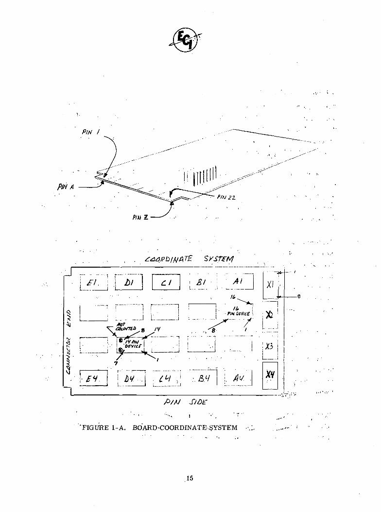
The board coordinate system is a straightforward layout defined in Figure 1-A. Each
board is capable of holding 24 sockets although only those required for a given circuitwere used. All of the sockets used were 16 pin although in many cases only 14 pin
devices were used. Where 14 pin devices were used, the pins 8 and 9 of the socketwere not counted and the remaining 14 pins were counted for device correspondence, as
shown in the illustration. These coordinates are labeled for each device on the
schematics discussed in this section.
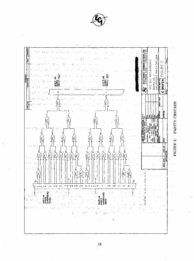
3,3.1 Supervisory Parity Checker; Board No. 2 (Figure 2)
This circuit is,;comprised of a parallel tree of exclusive OR's which monitors the 19 bits
of information stored in the parallel storage registers. The parallel tree was constructedto minimize the propagation delay experienced between the. time that the new information
is entered and the validating state is set at the output. Valid parity enables the decoders
(reference Figure 1).
There are two parity checkers per board with separate power inputs for each. However,
both are operated from the same supply .(A; B, C or D)-and one checker .monitors a one's
register while the other monitors the corresponding zeros register.
14
PIN I
A^ Plu 22.
ftU Z
J£Aai? D ii(iA ?*£
j L XI
• PIM Device \ •• Y)
"-•/' i
— I
XY
"FIGURE 1-A. BOARD^COORDINATB.SYSTEM
15
p
00
UJcr
do
Q- O<r CD
!'g Q
~ o
= • i ?
s = s
|l
uwwu
<M
w
.
16
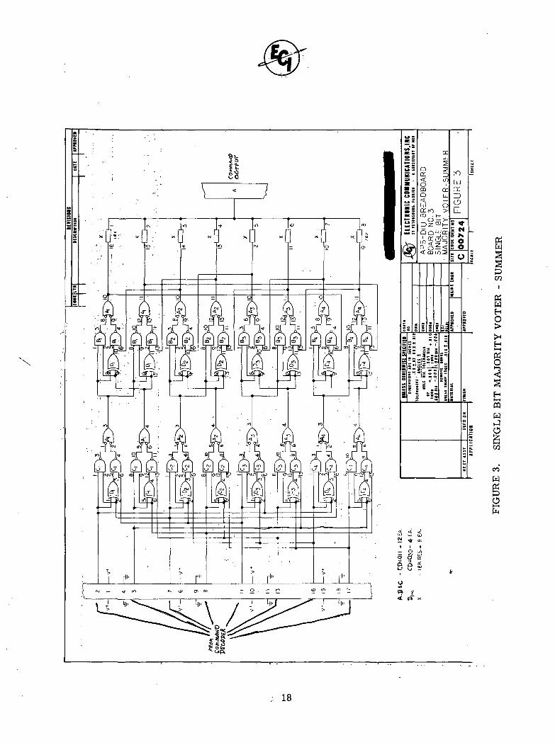
3.3.2 Single Bit Majority Voter; Board No. 3 (Figure 3)
This circuit collects the command data from the eight decoders and inter-majority :
votes on two levels to a resistive summing network outputted to one point. The
scheme is oriented td eliminate any two hard-failed or floated inputs by reducing this :
indication to a single'line within the first level of majority voters. The second level ofmajority voters performs a bit-correction operation such that the summed outputs are ;
all in the correct state. Above this, the module in itself is immune to two device .
failures. Open \ resistors at the output will not contribute any degradation to the ;
signal state. Shorted output gates (two) will deteriorate the output logic level by 25% : ,
which leaves a 25% margin of additional level certainty. Two wrong states at the out- :puts of the first level of majority voters could not result in more than two wrong states
at the summing resistor inputs resulting in, again a 25% degradation.
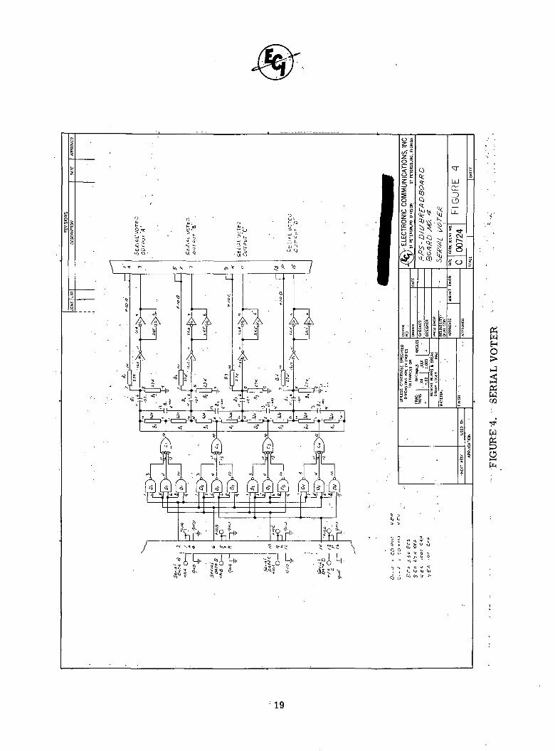
3.3.3 Serial Voter; Board No. 4 (Figure 4) ;
This circuit provides bit correction and correlation from four different but simultaneous
serial inputs to four separate outputs.
A set of four majority voters views the input signals in four sets of three each and out-
puts corrected data against a single incorrect input each. Where two inputs to a
majority voter are in some hard failure mode (high, low or open), there is no contribu-
tion to the RC summingnetwork by that majority voter. Two majority voters may either
fail or view two failed inputs and the summing network will still provide corrected datato the four recovery/driver output gates. :
(1) Open resistors are considered the prime resistor failure mode in the APS/DIUdesigns. Within a final package employing LSI techniques, most of these resistorswill necessarily be thin film deposit resistors. Shorted thin film or metal film resis-tors is about 0. 01% of the probability of an open failure mode. To additionally protectagains the short failure mode, series resistors may be added which increas the [probability of an open failure mode. It is, therefore, reasonable to ignore the shortingfailure mode because of its low impact on system reliability.
17
0 0 0 0 0 0 0 0 0 0
w
(6WEHO
HHH
OQ
CO
CO
W
; 18
o 3
II
o<-> io %z °2 'CC. o
o %
LJor
LJ_
oo
o
s
5| £•
$. > Vj »j V y
Q Q ^ .^ o -y * o •-
"ft ^ O 3
> •> ^ ^r « ^I , H j U j l u U i
^ - Oi oa 3- >
tfwHo
CO
O
; 19

This circuit takes decided advantage of the 50% switching characteristics of CMOS
logic devices. A bias network is added to the inputs of the recovery gates such that
they may operate at lower input logic swings than normally required. The output gatesare paralleled to provide additional drive to the lines within the breadboard.
The;circuit will :pei|form with no noted changes in the output if two of the input lines
are shorted to ground, tied high, combined high and low or have different interferingsignals of any frequencies. Two sets of different signals cause considerable confusion
; because the circuit cannot determine which two are correct.
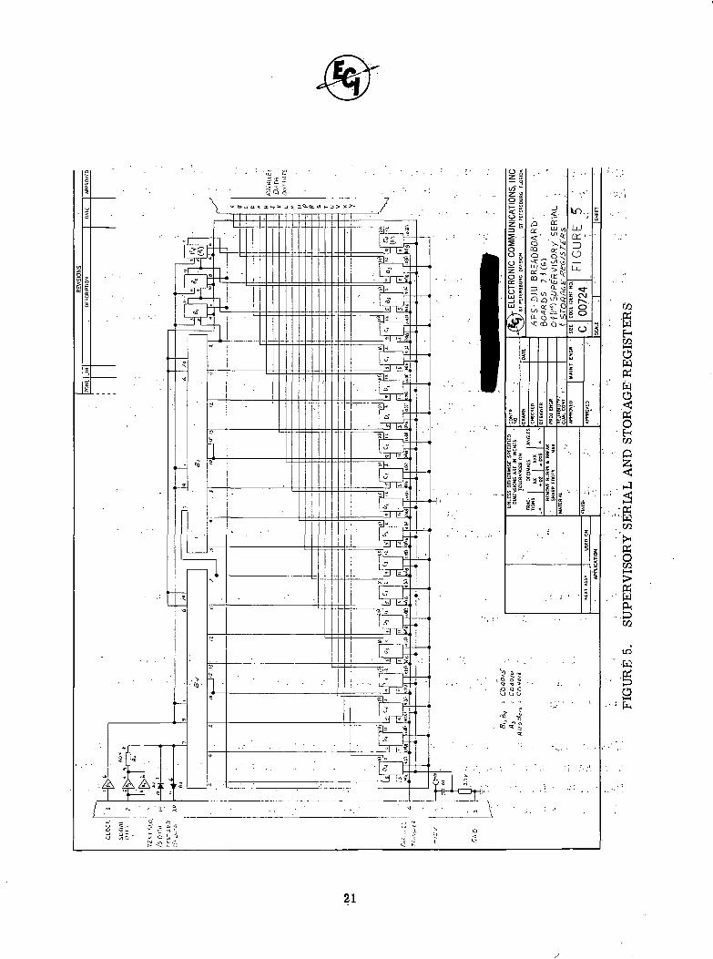
3.3.4 : Supervisory Serial and Storage Registers; Board Nos. 6 & 7 (Figure 5)
This schematic illustrates two types of similar boards, one for the 1's information and
;one for;the;6's information. The difference is in the information taken off of the
storage; elements XQ of Q)o .
The clock and data are buffered coming on to the board (not needed in LSI format) and
they feed a 19 bit serial register. .The "parallel transfer" input is, in fact, the "end-. of-word" pulse detected within the System Clock Generator and this pulse loads the
inputted data into the storage elements.
The information remains in storage for 20 microseconds while the next word (or "all-zero "pattern) is shifted in. :
Of the 19 bits shown outputted, only 8 bits are employed in the APS/DIU breadboard.This added capability is provided in the event that there are changes to the system
.requirements.
< . • ' , ' . ' .
The serial data input is buffered by two parallel buffers and feeds a 40 K resistor which
is in series with the input to the shift register. At this junction, shown on the schematic,
two diodes also input at .this point labeled "Test Sequencer '!' Data" and "Test Sequencer
'0' Data" respectively. Here, the Test Sequencer inputs the assigned words during
20
H£2OWtfWO<'§
Hto
•tf' Wen
w
to
w
21

APS/DIU."self-test," and the diode configuration provides forced one's or forced zero'sto override whatever information may be on the buffer at that given time. In the normaloperating mode, these diodes are open.
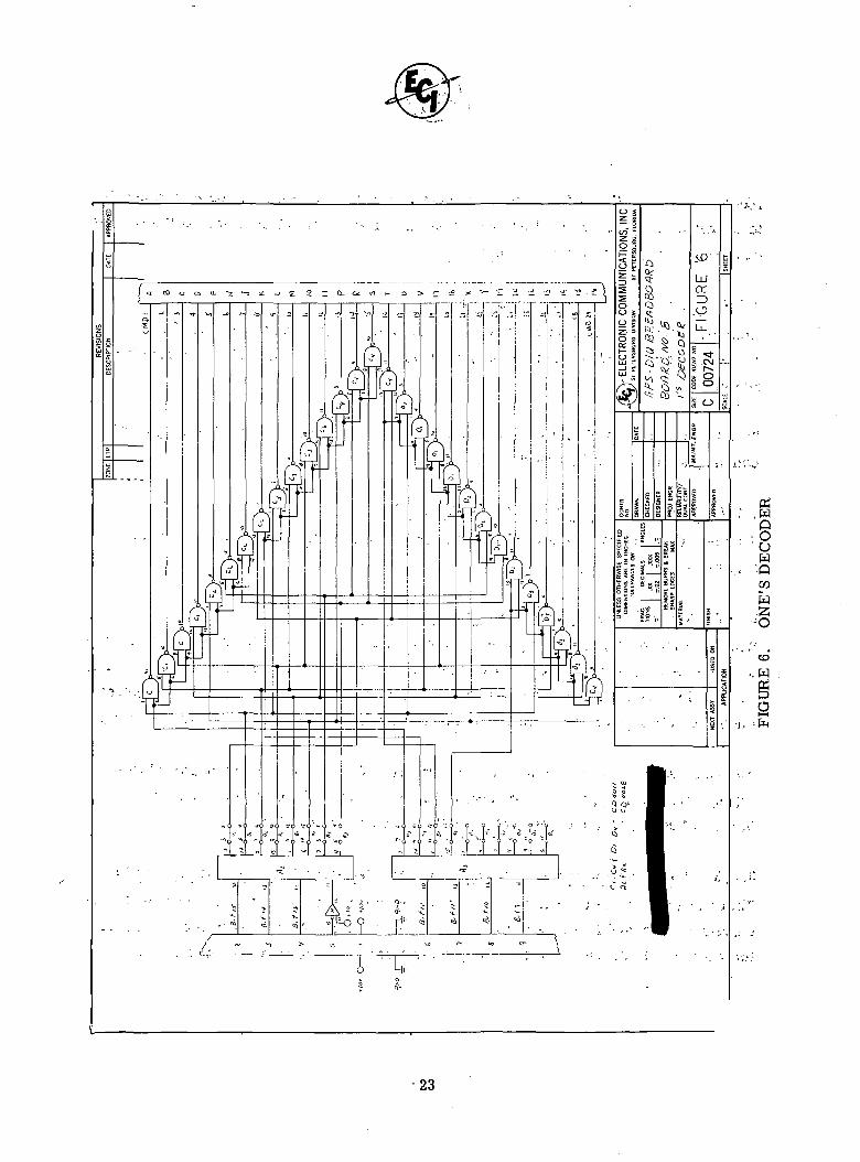
3.3=5 One's Decoder; Board No. 8 (Figure 6)
This circuit has for its inputs, the eight encoded bits of the supervisory word that isloaded"into the "ones" storage registers. There is a decoder for each of the four "ones"registers. ; :
' . . . / ! " •'" • ' ' '
The decoding is straight forward binary-to-decimal decoding to output 1 of 29 possiblecommands as a'zero'in a field of'one's. .
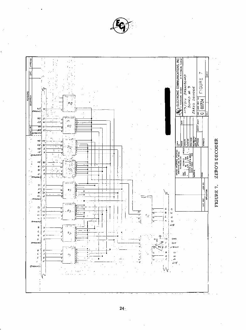
3.3o6' Zero's Decoder; Board No. 9 (Figure 7)
This board is.identical to Board No. 8 except that it gets its inputs from the zero's• ' • ' - " *
.registers. ; . - , ' ' • ' - . • ' .
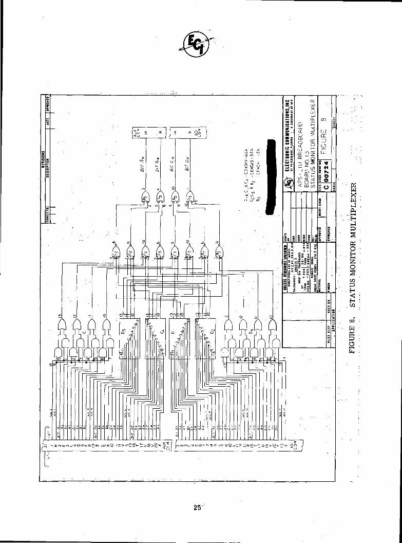
3. 3i7 Status Monitor Multiplexer; Board No. 13 (Figure 8) .'.
Sixteen of these boards are required to comprise the complete Status Monitor Multiplexerin four sets of four each. Each board has six 2-wide 4-bit multiplexers with appropriatecontrol lines to steer one of the twelve 4-bit selected inputs to the output.. The control
"lines are activated in accordance with the status word requested and by board location.
As can be seen by the diagram, straight forward AND-OR circuitry is employed withappropriate steering gates to the output. These circuits will present a unique problemin the LSI configuration because of the I/O pin.limitation per chip. ;
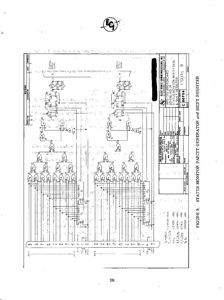
3. 3. 8 Status Monitor Parity Generator and Shift Register; Board No. 14 (Figure 9)
This circuit receives the selected data from the multiplexer and the load and timed clocksignals are inputted from the timing and control circuits. A parallel tree parity genera-tor views the 16 bit input and the parity bit is loaded into the registers with the data.
22
§0w
*QOT
H
CD
. w
23
poowQW
bffiw
t-wBo
24
X!HJft
gOSCQ
HCO
25-
WHraH-*
O-wKH
CO
•o
gH
WO
PM
«EH
'S'
-o
EH03
O5
O
26;
Bit "one" is always preset to a "1" and bit "nineteen" is always preset to a "0". The
remaining 17 bits are data plus parity. ' :
There are two shift .registers with parity generators per board and two boards required
for the APS/DIU.
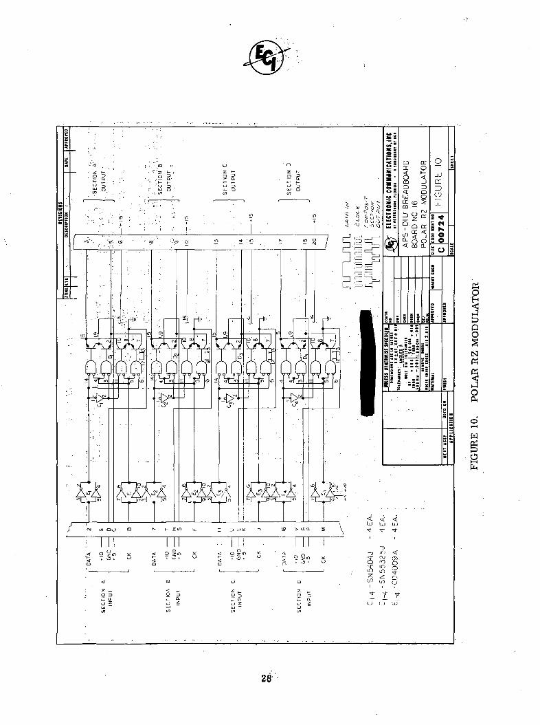
' '• ' ". .-. f3.3.9 Polar RZ Modulator; Board No. 16 (Figure 10)
To drive the shielded twisted-pair lines to the Data Terminal from the APS/DIU with •
Polar RZ data, a core memory driver (S/N 55325) from Texas Instruments, was select-;
ed to perform as a line driver. Here, the polar RZ waveform can be achieved directly , •
utilizing the internal logic configuration with data and clock as inputs. The device has ;:
600 ma driving capability which is more than sufficient to drive the 75 ohm line. '.
impedance.
The input buffers perform a CMOS-to-TTL conversion for both the data and clock and
these feed the polar RZ drivers. Each polar RZ driver has a transistor configuration
on its output such that in the "one" state, one side of the line is tied to +5 while the ;
other is tied to ground. In the "zero" state, the opposite line is tied to +5 while its
alternate is grounded. During the "no-data" state, both output lines are open. The wave-
forms are shown on the schematic. . . , '
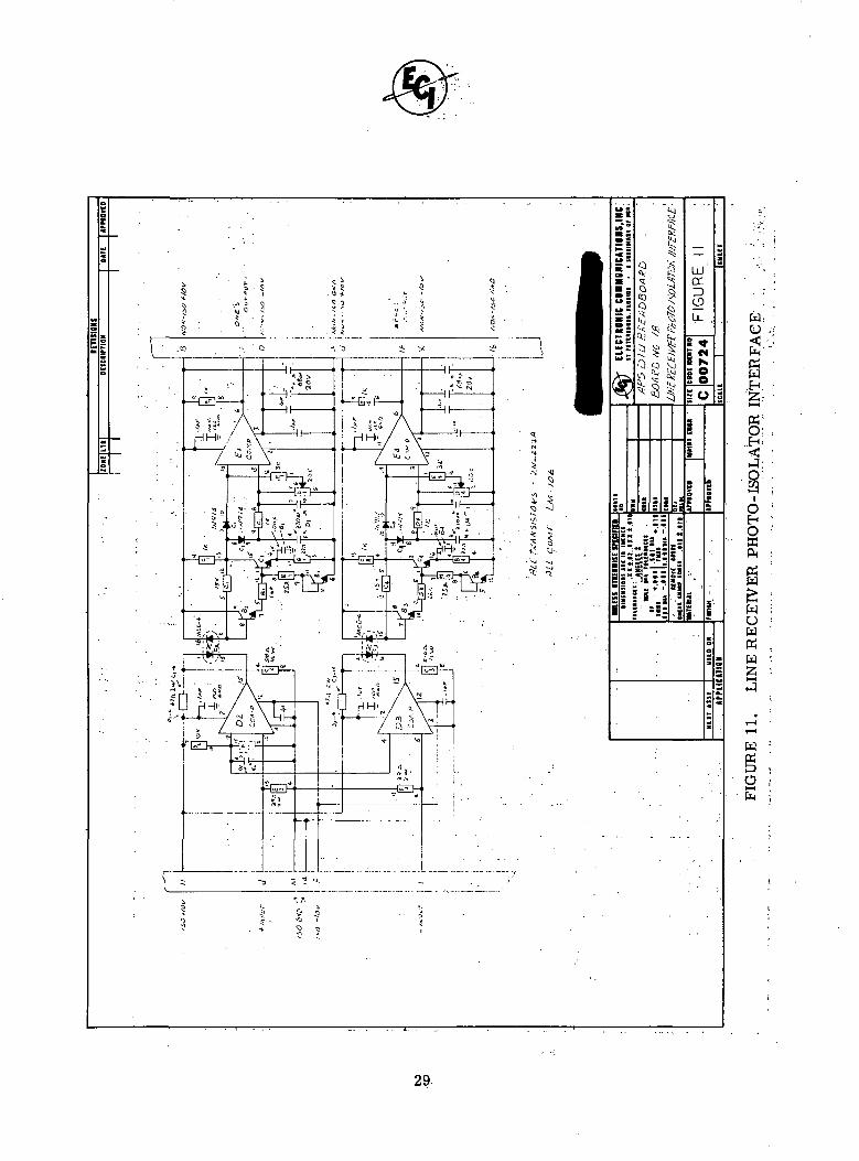
3.3olO Line Receiver-Photo Isolator Interface Circuit; Board No. 18 (Figure 11) .
This circuit provides the isolation and data recovery from each line that inputs to the
ISVC circuits. The primary of the board is powered separately from the remainder of
the APS/DIUo Two comparators sense the "ones" and "zero's" separately and drive •
photo-isolator diodes. The network on the output of the photo-diodes provides both gain
and high speed recovery of the bit waveshapes. The diode network along with the bias-
ing configuration at the input of the output comparator, provides temperature compensa-
tion for the temperature characteristics of the photo-diode. : : '
27'
§QO
N
oi—iH
28
ii
!--4
§§
cr
*< <Sj :?
^ fc51 § S
O Q ^
^ ^ S 1 ^oo
= 0
io ; i s s 25S S
g;
OH
§ft
tfw
HOw
W ;
O i*-H
29
The photo-isolating concept utilized in this circuit is not a new or difficult circuit to
design.. However,'.making a photo-isolator perform consistently throughout the temp-
erature; of T55°C to .+ 125°C is difficult because of the photo-diode characteristics at
+ 125°C. As a result, this circuit became more complex than is "reasonable" for itsfunction. An industry search reveals that other materials (different from the gallieum
arsenide jused in:thesMCD-4) were being investigated for application in photo-isolation
and devices should be available during the last quarter of 1972. The circuit developed
for the APS/DIU proves the feasibility of this technique; better devices would certainly
reduce, the'functional complexity. .
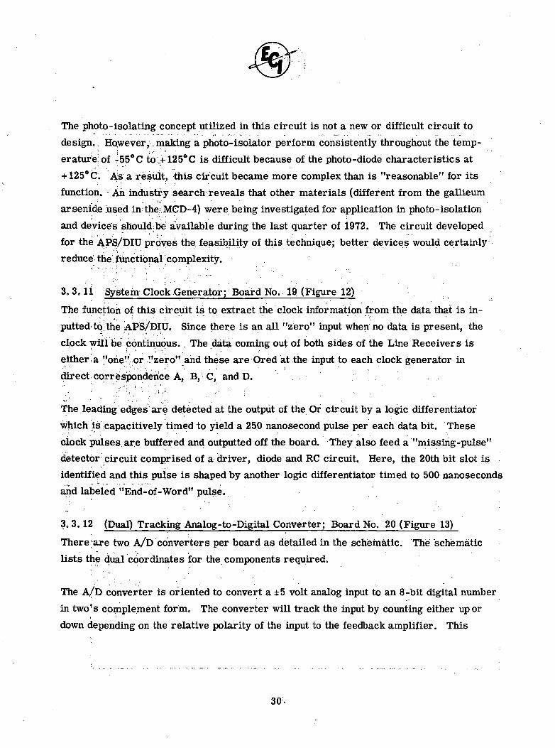
3, 3. li System Clock Generator; Board No. 19 (Figure 12)
The function of this circuit is to extract the clock information from the data that is in-
putted'to; the APS/DIUc Since there is an all "zero" input when no data is present, the
clock will be continuous. The data coming out of both sides of the Line Receivers is
either a "one" or '.'zero" and these are Ored at the input to each clock generator in
direct correspondence A, B,'-Cj and D.
The leading edges are detected at the output of the Or circuit by a logic differentiator
which is jcapacitively timed to yield a 250 nanosecond pulse per each data bit. These
clock pulses are buffered and outputted off the board. They also feed a "missing-pulse"detector circuit comprised of a driver, diode and RC circuit. Here, the 20th bit slot isidentified and this pulse is shaped by another logic differentiator timed to 500 nanosecondsand labeled "End-of-Word" pulse.,
3. 3.12 (Dual) Tracking Analog-to-Digital Converter; Board No. 20 (Figure 13)
There are two A/D converters per board as detailed in the schematic. The schematic
lists the dual coordinates for the components required.
The A/D converter is oriented to convert a ±5 volt analog input to an 8-bit digital number
in two's complement form. The converter will track the input by counting either up or
down depending on the relative polarity of the input to the feedback amplifier. This
30-
•g'
KW•2wousw
CM»-H
'w
31,
<L
r -•! ;-
Q,
H" "I -L_U ,,
VJ"4 ^s, _. „• , . ;_ _. ;_
x > ^ ^. z
J; i, v, 2 ^» V , H. Hi,
i i i !
I.O
O
O
isQ
COi-H
'•• W
O
' ' "£
allows the information to be accessed at any time except during the actual clock period
which is approximately 2 microsecond wide.
The up/down count mode of the counter is controlled by a single comparator in conjune-
tion with a flip-flop. The counter will count until the D/A converter in the feedback
loop equals the -amplitude of the input. Nine (9) bits are shown to be outputted but only
8 are employed. The 9th bit or LSB continues to complement with each clock pulse as
does the up/down count mode once the A/D converter has reached equilibrium. ;
The input clock is 12. 5 Kc with a clock pulse width approximately 2 microseconds. This
permits maximum access time to the converter and eliminates the clocking effect of —
comparator oscillations when the A/D converter is on the near-edge of equilibrium. >
3.3.13 Emergency Shutoff Monitor; Board No. 21 (Figure 14)
This circuit is one of two boards cpmprising the Emergency Shutoff Monitor. Here, the
logic, in triplex, seeks several faults which are unique to the engine itself and causes
closure of the Emergency Shutoff Valve. The faults include (1) an uncommanded engine
burn which is detected either by sensing unwarranted chamber pressure or a closure in
the engine-valve switches; (2) a drop in line pressure accompanied by a closure in the
engine-valve switches which is also not commanded. . . . . . ;
These conditions are sensed andORed at the circuit output in three sets of. three NOR
gates. Each set of NOR gates will feed a separate series driver inBoard No. 22.
As is shown on the schematic, the inputs to this board use resistive isolation to the
inputs to each gate. This is to isolate similar circuits which operate from the same :
source such that any two inputs may assume a failure mode (shorted high or low) without
disturbing the logic level of the input to the third input.
3. 3.14 Emergency Shutoff Monitor; Board No. 22 (Figure 15)
This board receives as its inputs, the decisions made on Board No. 21 and the external
33
§EH
faoH
o
w
*
w
o
34
AAAAAAAA/^AAAAAA^A/
wJ.
O'£ao
CO
O
WOtfww
inTH
w
35
command for e'mergency shutoff; Again, the logic and drivers are configured in triplex/• • ^
parallel to provide; dual failure immunity.
The emergency shutoff and reset commands from the "Input Data Validity Comparison"
circuitry feed a triplex set of three latches. The latches feed a set of CD 4010's which
are used for CMOS-to-TTL conversion for both the external commands and the informa-
tion fed in from Board No. 21. These data are ORed in TTL 5412's which are open-
collector gates used to control the drivers. Each driver set is comprised of three NPN
transistors gated on essentially in parallel (but by different sources) which drive a set
olPNP transistors in, series. Here, all three inputs must be identical to turn thedriver^ "on" which protects a driver set against two shorted transistors. ,As shown,there are three jdriver sets in parallel which protect against two open-failed transistors.
During "Self-Test" the Emergency Shutoff Monitor is inhibited both on Board No. 21 and
Board'NOo 22. On Bpard No 22, it is inhibited at the latches such that ESO does not
get activated during*'the input circuit tests.
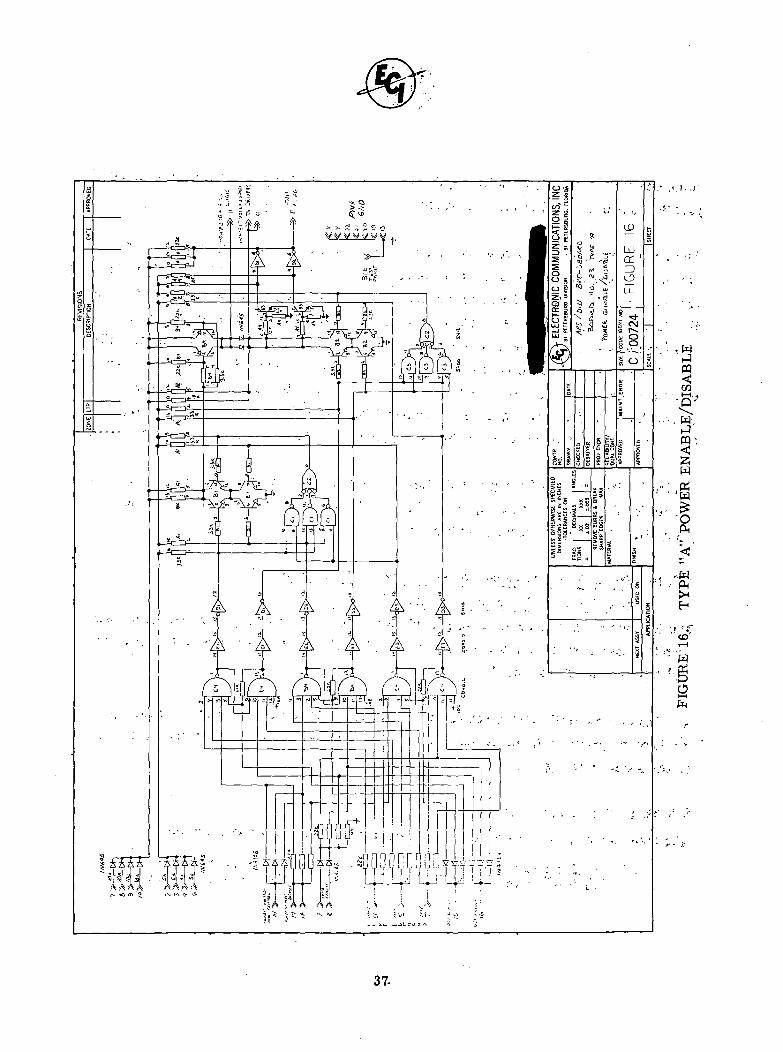
3:3.15 ,-. Power Enable/Disable Module; Types "A", "B" and "C"
'•' 'Board No. 23 (Figures 16, 17 and 18)
The fxinction of these-circuits is to provide power to the Firing Logic boards selectivelysuch that they operate in a sequence according to failure. The sequence will always be
"A"-to-"B"-to-"C"-to-"off." -
The Power Enable/Disable circuits will be discussed in order of sequence. Althoughall three do perform the same basic function, there are fundamental differences based
on the sequencing requirements. ' . " .
3o3ol5.1 Board Type "A" •
The input commands as shown on Figure 16, perform the following functions:
(1) "Inhibit Function Monitor Control"- This is a Test Sequencer inputwhich is active only during certain portions of the self-test activity
36
37-
w•4ffl
Q
H
CQ
Wtfwo
w
H
•
c-"•*"!
W
O
38'"
w•JfQ
COI—I
Q
"w
w
u
wAH
? H
39

to inhibit the associated Function Monitor from shutting down... -the power to "A" Firing Logic. „ As can be seen from the logic
configuration, a low at the Function Monitor Disable inputwould set the latches E4, D4 and C4 to an "off" state. Thislow is forced high by the inhibit input during Test Sequenceractivity so that the latch state is not altered.
(2) "Function Monitor Disable" - This signal comes from the FunctionMonitor as,an indication that Firing Logic "A" is not operating -correctly.,-,A low at this .input sets the latches to an "off" state .as discussed above.... - - - -
.; (3) "Auto Enable" - If this point were brought low, the latches -would set to an "on" state. However, because the idea of a"try-again" scheme was dropped in the design of the DIU,this input is tied high and not used in this module.
(4)' '-' "isyc Command-; Inhibit, Inhibit and Use"- These inputs are the.. ... ... ,:,,,redundancy override commands coming from the ISVC circuits.
The "use" input sets the latches to the "on" state and correspondsto the "use Firing Logic 'A™ command. J The two inhibit inputsset the latches to the "off" state and are, in fact, the "use FiringLogic 'B'" and "use Firing Logic 'C'" commands. Here, when a
"- ^Viring'Logic set different from "A" is programmed on, the^ ,> inhibit .command insures that "A" is off. . „ ,
(5) "Test Enable" and "Test Disable"- These inputs are Test Sequencerinputs and are only active during certain portion of the self-test.
The logic within the Power Enable/Disable function is a majority voted set driving quad-
transistor sets to either power or ground the Firing Logic power lines* The design
intent of the board is to yield single failure immunity in being able to turn power on to
the Firing Logic and to be dual-failure immune in being able to issue a "fail-flag" to
turn on the next backup.
This board, as well as types "B" and "C" should be implemented differently which has
been proven by this system breadboard study. This is discussed within the "Conclusions
and Recommendations" portion of this final report.
40
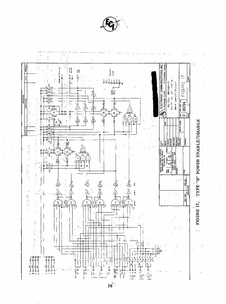
3.3.15.2 Board Type "B!1. -, •. , , . ,
The input commands to this board perform an identical function as listed for Board "A"
with the following exceptions: , . , ;. . . . - • • . - . . • '
a. Pin P receives its input from Power Enable/Disable Board, ...Type "A" which goes low if Board "A" was disabled auto-matically; . . - ' . - • • . - . . . • ' ' . ' ' - . , ' . ' " _,•- . " "
b. Board "B" will turn-on ONLY if Board "C" has not beenpreviously tried automatically and it is not presently onas indicated by the inputs on pins L, M, R, and V. ;' '
Table EE[ is a truth table indicating the states and the sequence of operation applicable
to all three boards., ..-, . . . . , -,,. • ..• • ' "• • •.. • _ • _ ,. •
Any board may be turned on manually regardless of the system state. "B" will turn on
automatically only if "A" failed and only if "C" is not on or has not been turned on auto-
matically, because o f a previous failure i n "B". , - • • - .
The diode configuration shown for the "A" Fail Flag, "C" Fail Flag and "C" Memory
permits these conditions of operation.- If either the "C" Memory or the "C" Fail Flag
are high, "B" cannot be turned on when, "A" Fail Flag goes low. ,. . ,
The Fail Flag mechanism for board "B" is derived from two sources and hardwire ORed
at the output. One source which drives parallel gates is the quad transistor voter located
at Bl; if this fails open, the Fail Flag will go low. The other source is the Firing Logic
power output which, when it goes low, a single gate string brings the Fail Flag low.
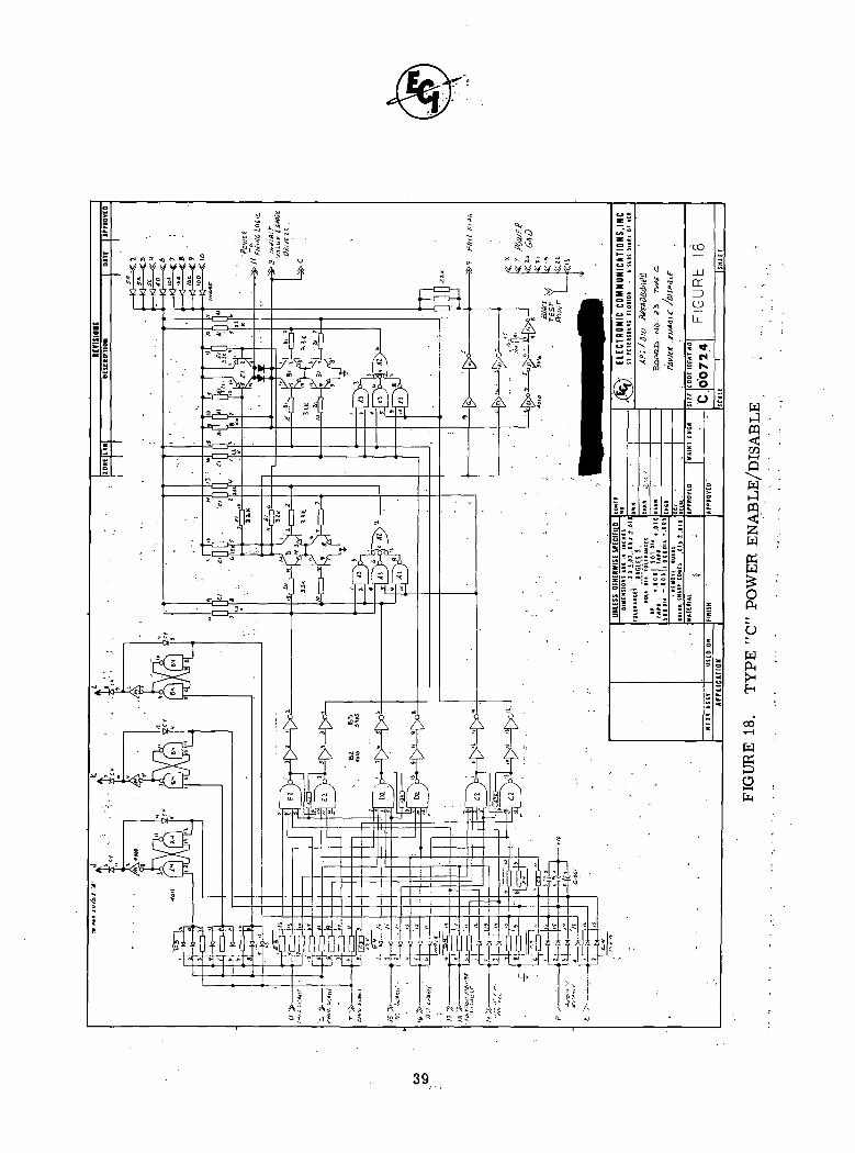
3.3.15.3 Board Type "C"
The input commands to this board function identically as those described for Board
Type "A" with exception to the "Automatic Enable" which inputs on pins P and R0 Here,,
both inputs must be low in order for the latches to be set to the "on" state. These inputs
come from the "A" and "B" Fail Flags and "C" will turn on until both have failed low.
When this occurs, the three latches X4, B4 and B4 shown at the top of the schematic
"memorize" that an automatic enable has been exercised,, This insures that, in the
41
STATES,,
MANUAL , . '" .
A commanded "on"B off; C off
B commanded "on"A off; ;C off r -
C commanded "on"A off; B off -
AUTOMATIC
A on; B.off; C off
A fail; Bon;:Coff
A fail; B i fail; C on "
Cfail; B fail; C fail
««^"FAIL FLAG
-.; - :. -,,
1
:0
: . . - . - 1 o '- ' • • • : • '-
1
". - . " • 0 . . . - : . . •,.
- : • - 0 ' • ' • ' •
0
"B"FAIL FLAG
•' • • '- • • - . • -
0
- ' - ' 1 - '
0
0
: • • • / ' - • ! - . . - ; . .
0
0
- - . f f /^»f .
FAIL FLAG
. , - •• , •,
0
0
• ' ' I ' - : ' • ' '
0
0
1
0
, t f /^ t t
MEMORY
0
0
0
0
. 0
1
i
TABLE m. POWER ENABLE/DISABLE FAILURE
SEQUENCE AND MANUAL CONTROL
event of "C" failing, "B" will not be turned back on. When these latches have been set,
their state is also diode ORed, into the enable junction such that the enable latches are
not held in a forced mode,, This will permit the "C" Function Monitor to,cause a disable
in the event of a :"C" Firing Logic failure. ;
The "memory'1 latches .will be reset if any manual command is issued whether it be to
turn on "A", "B" or "C". Once a manual command is issued, ;the system then returns,
to its automatic sequencing mode as a function of failure.
42 ':~
3.3.16 .Function Monitor; Board No. 24 (Figure 19) . .
This circuit monitors the Firing Logic valve and spark pulses, the Valve Switch closures
and the Chamber Pressure and determines if the system is performing normally within
the given logic set. There is an accompanying Function Monitor for each of the'Fir ing
Logic sets. - ' , . " ' , '
As shown.at the input, the comparisons of the above information is made in Exclusive
OR gates. The resultant states are ORed in Cl, C2 and C3 simultaneously. Here, a
one-shot is triggered and ANDed with the one-shot input signal after it has passed . .
through some delay gates.
The purpose of the one-shot is to create an inhibit-time to block out sensing the difference
between the valve and spark pulses and the difference between when the ignition is com-
manded and actual chamber pressure is detected. The test is, then, a kind of "reason-
ableness" test to verify that the system is performing approximately as expected. The
one-shot inhibit time is approximately 15 milliseconds.
If a failure were to occur, it would be detected within 15 milliseconds of turn-on command
and the majority voting quad-transistors would output a "low" to the Power Enable/Disable
logic to disable that Firing Logic set. .. •„ " • ;.•• .-.-,.-
Two failures that would majority-vote to cause a disable signal would eliminate that
Firing Logic set and turn on the next backup. Two failures-that would cause failure to
indicate a disable signal leaves the system either normal or vulnerable to a third failure
occurring somewhere in the Firing Logic. Manual control would then be required to 'switch over to ar working backup logic set. . . . ~ '• , '
3.3.17 Firing Logic; Board No. 25 (Figure 20)
This circuit executes the "turn-on" and "turn-off" commands outputted by the ISVC
circuits. Upon receipt of the "turn-on" command, the logic starts the ignition pulse,
waits 10 milliseconds and begins the valve pulse, holds both pulses on until it receives
43
OHH
O
3§HHH
§s
Uȣ3
44 •
-
OsO
OCM
45.

a "turn-off" command or clocks out 50 milliseconds; whichever comes first.
If a "turn-off"- command occurs first, the logic turns off the valve 10 milliseconds after
receipt of turn-off to compensate for the delayed turn-on. Then, in an additional 10
milliseconds, it turns off the ignition pulse. If it is permitted to time-out to 50 milli-
seconds, the valve pulse will remain on for 50 milliseconds.and then it.is turned off
while the ignition pulse "stays on for an additional 10 milliseconds. Figure 21 illustrates
this timing. , - ?
Although this relative valve and spark timing is subject to change, the thinking was toinsure that burning would start by initiating the spark prior to the entry of fuel andmaintaining that spark until after the valves were closed, insuring complete burning
without wetting the spark points. This insures that each burn cycle is initiated withd r y points. . , . . - . , , . . . . . . . . . . . . .
.' "-. -v- '• -. i
Functionally, the process begins with the 20 microseconds "on" command being received
on pin 6. This sets latch E1/E2 which also sets latch B1/D2 to turn on the "spark" pulse.
The change-in-state of latch E1/E2 is detected by the logic differentiator D1/E2/E2 to
trigger the one-shot (10 ms) C2/C1. The end of the one-shot period is detected by thelogic differentiator B1/B1/B1 which creates a pulse that is NANDed in gate A2(9). This
sets latch A1/A2 to begin the valve pulse.
Now, the valve and spark pulses continue until a turn-off command is received at the
latch E1/E2 either by ISVC command or by automatic turn-off as timed out by thecounter E3/D3/C3.
Once the latch E1/E2 'is reset, the logic differentiator D1/D1/D1 senses this changeand re-triggers the one-shot. The logic differentiator B1/B1/B1 recognizes the end of
the one-shot period and resets the valve pulse la'tch A1/A2. This delays the turn-off of
the valve the same amount of time that it was delayed in turn-on. The logic differentiator
A1/A1/A1 recognizes that the valve pulse latch Was reset and it steers another trigger
46
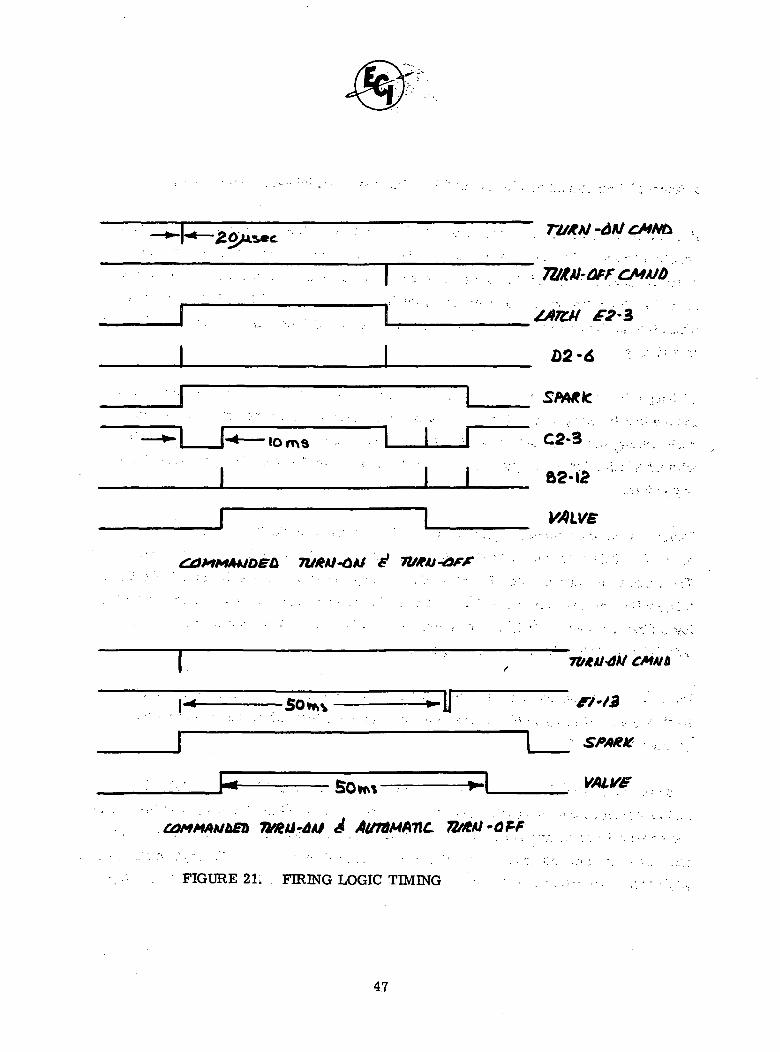
10 ms
i
£2-Z
D2-6
SfAtlC
C2-3
VAIVS
I"*" 50 *s
COMMAUbEb
•ITSPAKK
VAIM?
Tbfiti -GIF
FIGURE 21. FIRING LOGIC TIMING
47.
pulse back to the one-shot. Again, a one-shot pulse is generated and detected byB1/B1/B1. , the last differentiator pulse then resets the spark latch B1/D2. The '
string of inverters B2 delays the change-in-state of the valve pulse latch from reachinggate D2; until a^ter the one-shot pulse has been restarted.
In review, the one-shot ;C2/C1 is used to generate three time delays for each enginefiring; the first to delay the valve-on T amount after spark has beenturned on; thesecond to delay valve^off T amount to maintain proper valve duration; and the third toturn-off the spark T amount after the valve has been turned off.
To^keep the: engine "on" full time, a command must be received more frequently than50 ms to inhibit the automatic turn-off.
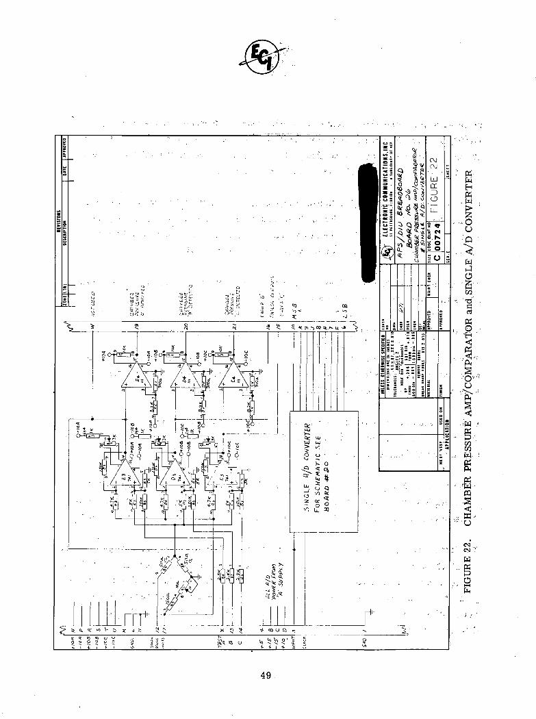
3,3.18 Chamber;Pressure Amplifier/Comparator and A/D Converter;Board No. 26, (Figure 22)
This circuit monitors the Chamber Pressure Transducer with an internal strain gaugeassumed to have a nominal resistance of 511 ohms. The amplifiers are presentlyscaled to output 1 volt per 10 ohm change in the strain gauge.
Both the type of transducer and the amplifier scaling as assumed to be subject to change.Therefore, the breadboard was fabricated with plug-in flexibility such that the configura-tion arid/or scaling is easily altered.
In the circuit, three amplifiers monitor a single bridge and feed three comparators.The amplifiers are scaled for approximately 1 volt/10 ohm change, in the bridge and thethreshold comparators will switch at approximately a 1 volt change in the amplifiers.
The linear outputs of the amplifiers is digitized by A/D Converters (previously discussed)one of .which is fabricated on this board and monitors Chamber Pressure Amplifier "A". ,The A/D information is for status monitoring information. The threshold comparatorsperform a "reasonableness" test to verify the presence of a chamber burn and thisinformation is used in the Function Monitors and the Emergency Shutoff Monitor asdiscussed before.
HK
- W
55,0o
wjo
'"§
OJ
tfo•EH
.•'O'u
COCQH,
"m•S
u
CMCSI
49
In a LSIvversion of an APS/DIU,., this circuit.would be .fabricated using,.micrpelec.tronic
technology with chip rand-wire bonding and film resistors with manual trim for scaling
and null adjustments;^Potentiometers were included in the breadboard but would not
be used in a final version.
3 0 3ol9 Spark Driver; Board No. 27:; Valve Driver; Board No. 28 (Figure 23)
The Spark and Valve Drivers are'identical in schematic configuration with the exception
to circuit values because of the different load capabilities.
The Spark Driver was assumed to require 1 ampere drive and the Valve Driver was"!*'• .' ' "^ '•'; "• *• -;••*
assumed toi.require 50 ma drive capability. Both of these may be altered in either
direction by,altering resistor values or the boards may be interchanged as required.-- '• ••Iv^,..*^;-* C•^ 4fr'!^^%;. •' •• ' " • :
Each board is c'omprised of three drivers each of which is associated with a Firing
Logic set. *-• Each^driyer has three .transistors in series two of which are intended for''*•"' 'ji '-'.-i* i. ''*•"'"« • . '.•?; .• •
failure inhibit arid theithird for 'modulate* or turn-on of the driver.' "
. -
TKe1 driveri's are interfaced with CD4009's configured for a TTL interface to 5416's.
These control 2N2222 drive transistors which turn on the PNP 2N5781 drivers.
Each driver has a current-pipnitoring resistor which is one ohm for the Spark Driver'""".-•. •' . i
and 20 ohms.for the !\&lve Driver. Here, the on-state would indicate one volt for each
driver. This voltage is interfaced to, the monitoring A/D Converters with a transistor
and two'resistors. Referring to the schematic, transistor Al at pins 1, 2 and 3 has a
IKfresistor in series with its emitter and it is tied to 28V(a). Assuming that the two
PNP's will have near-tracking base-emitter voltages, the voltage then across the
current-sensing resistor and the drive transistor (Al-14,, 15, 16) emitter-base junctions
is fixed by the driver load. Since this same voltage is across the monitoring transistor
(Al-1, 2, 3) base emitter plus IK resistor string, the IK resistor then becomes a
current determining element for the collector current which flows through the 5K . [
resistor. The'scaling, then is set based on 1 volt across IK or 1 ma; SK'at 1 ma is
5 volts which is the .'input to the A/D Converter.
50.-
51'-

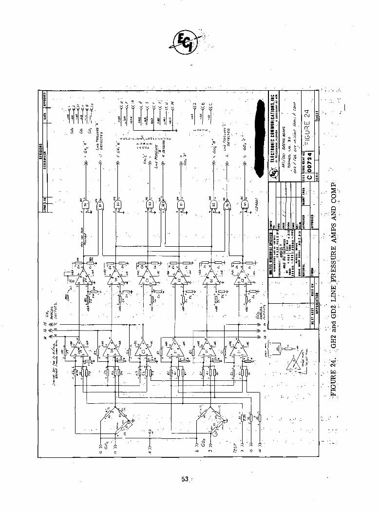
3. 3. 20 Line-Pressure Amplifier/Comparator; Board No. 30 (Figure 24)
The function of this circuit is to monitor pressure transducers which indicate fuel and
oxidizer line pressures. As with the previously discussed Chamber Pressure Amplifier,
a strairi-guage nominal value of 511 ohms was assumed and the amplifiers are nominally
scaled at approximately 1 volt per 10 ohm change. And, as before, the amplifiers feed
A/D Converters and the comparators shown.
Functionally, the circuit senses a drop in pressure below some acceptable level yet tobe, definted.' However, once the comparators sense this drop, the information is fed to
the Emergency Shutoff Monitor to disable the engine. The ESO data is the outputs of the
NOR gate'sjpl,; B2 and B3. The remaining gates are used for inverters which feed the
binary' status to the status monitor for reporting to the data bus.
The logic records hard failure states and the A/D Converters Monitor slower degradation.
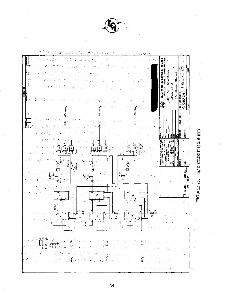
3.3.21 ;A/t).Clocks; Board No. 31 (Figure 25)
The function of this board is to provide a 12. 5 KHz clock for the tracking A/D Converters.Therelare three generators each sensing a different "end-of-word" source at 50 KHz
and each divides this frequency by 4. Pulse shaping is accomplished with an RC circuitfeeding-the inverters ;D1, D2 and D3 such that the pulse width is approximately two (2)
microseconds. The remaining gates are used in a buffer configuration for driving thelines to the A/D Converters.
In addition, there is inter-synchronization added between the three generators using
150 pf capacitors cross-coupled to the reset lines of the flip-flop dividers.' This insuresthat one of the generators becomes "command" and that the remaining will slave-
synchronize. It is academic which generator has command or that synchronization truly
exist. The feature was added for test arid monitoring convenience,,
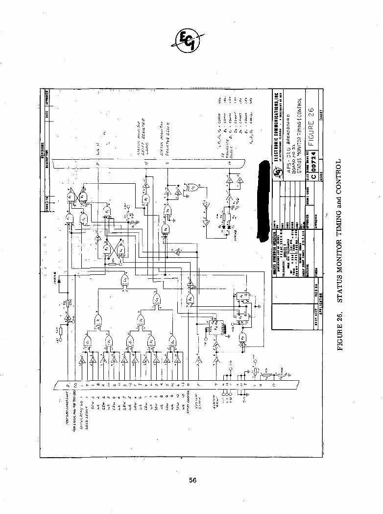
3.3.22 Status Monitor Timing and Control; Board No. 32 (Figure 26)
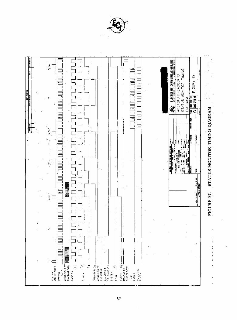
This circuit both enables the Status Monitor Multiplexers and sets up the timing for out-putting the Status Monitor,word selected to the Polar RZ Modulators.
52
ou.-
'<ft
w
CQ
w'
(SioO•o
CQffi
O
.(M
W
53 ;•
Ow10
(M*
oSop
W
54

The Status Monitor word request command inputs to the inverters as shown on the
schematic from the ISVC circuitry. The inverter outputs are fed to the multiplexers :,.
and a set of Exclusive OR's. Here, additional information verification is performed in - :
that the Exclusive OR tree will only respond if the number of request commands is odd : :
(1, 3, 5, etc.)- One command is truly valid. The probability of receiving three com- \
mands is extremely remote and receiving two simultaneous commands is rejected. .;" • - . /
Once the command is received, latch B1/B1 is set and begins the sequence as illustrated
in Figure 27, the Status Monitor Timing Diagram. , i
The first pulse outputted is the "status monitor load" pulse which is generated by the : ?
state of E4-Q3 and the fact that a command has been received. This loads the informa-• :
tion into the Status Monitor serial registers of Board 14. With this event, a two bit
counter is enabled which counts off 40 microseconds or two "end-of-word" cycles. ;
When'XI and X2 of D4 reach the states of low-high respectively, the Status Monitor \
clocking and Polar RZ clocking trains are developed,, These are used to shift the data
out. The end of this event is decoded to reset the B1/B1 latch back to the standby state. >
An alternate mode is operated during the "Self-Test" sequence of the APS/DIU. Because!
the self-test sequence does iterate all the system commands, the Status Monitor Timing
and Control module must ignore this function or all status words would be outputted.
Consequently, the B2/C1 latch recognizes the self-test command and is armed to inhibit ;
latch B1/B1 from reacting to the self-test generated words.
Once the self-test is complete, a status word is available at the multiplexer and the
Test Sequencer issues a "load/send" pulse to the Status Monitor. At this time, the •
registers are loaded and latch B1/B1 initiates the send cycle as before. •
The inverters E3 that output to pin S shape up the clock pulses to the registers and the ;
C2 X-OR gate and additional E3 inverters provide sufficient delay, along with the diode-
resistor-capacitor network to the C3 inverters to provide the Polar RZ clock. Here, it .
is insured that the data and clock skewing is aligned such that the outputs of the Polar RZ
provide the proper waveforms- :•
55
Otf
OO
O
§EH
CQ13H<HCO
COCM
W
56
— <\J fO
U) <O Q
o'S5 o:
a o .* z x xSQ -0 u
CL _ j uj O *nJ ^ u. <r S. 5>- w o o Q S >-Z Q u j ^ L i J ^ ^- Z
o o w 2' u> >? o' oo 5 O l n t t ( / ) UJ O
U)
MCC.
QC i:
c ~ < ^ O JO
O -I
25
gl
2"m a:Q o
CD o
l/l Q
hlilililgbl
UJCf.
s o~ o~o
PS'o
o5
§
CO£>•H<H
C-(M
w.
ot-Hfn,
57
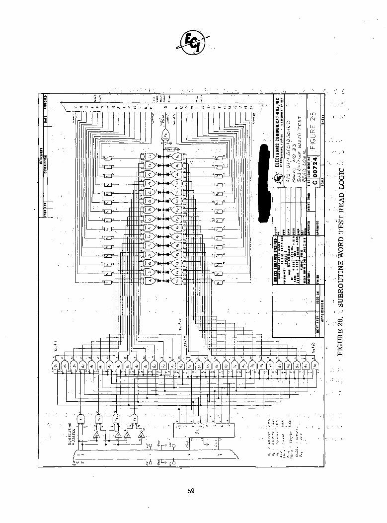
3.3.23 Subroutine Word Test Read Logic; Board No. 33 (Figure 28)
This logic is part of the "Test Sequencer" function and operates only during the "self-
test" exercise. : : - - _ \
As a function of the self-test, a subroutine is iterated several times that inserts all the
commands of the APS/DIU into the front end of the ISVC circuits. The results are (or
should be) a series of decoded commands providing the ISVC circuits are performing
correctly. ..
As these commands are iterated, the Subroutine Word Test Read Logic verifies that
each word appears as it should and that there is only one command at that time, (a ,,•
single 'zero', in a field of one's). As the commands are generated by an address counter
on the Subroutine Control Logic, Board No. 36, the shift register X3 is clocked while
the gate logic of XI and X2 decode the states of bits 4 and 5 of the address counter. The
combinations of these outputs are NANDed in the test gates such that there is corre-
spondence in the 'zero' out of the test gates with each 'zero' sensed at the wojg input.
That iSj test I/word; 1, test 2/word 2, etc.
For a.continuous normal operation, the outputs of the Exclusive-ORs will remain at
zero during the word test time. A failure inputs a 'one' or high at the diode OR function
which drives the output "word error" gate:C3.
'.'••' "" ' . . ' ' , . . . . . . . . .
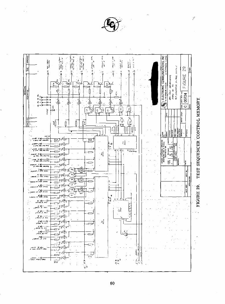
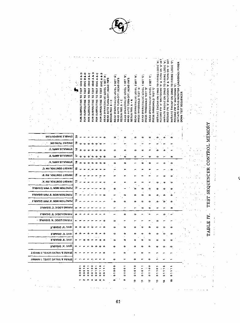
3J 3. 24 Test Sequencer Control Memory; Board No. 34 (Figure 29)
The function of this board is to place the APS/DIU in a series of unique configurations
such that specific tests may be performed to verify individually the given portions of the
redundancy. As with the rest of the Test Sequencer logic, this board only operates
during the "self-test" exercise and, in fact, it is powered down at all other times.
The control memory receives its clocking information from the Test Sequencer Timing
and Control logic, Board No. 35. The clock drives the synchronous counter Cl, which
generates the address data for the Read Only Memories Dl, D2 and C2. Table IV is the
58
.o3
w•E-)
.1.w
o
OOCM
59
K
§W
SH
tfWu.gWE>O1
WraH03
•a
60
a Q
r is
vc c
&r
ISV
C B
&
g SUJ UJz z
RU
N
SU
BR
OU
T
RU
N S
UB
RO
UT
u
r is
vc B
&UJ1-Ol-UlZ
RU
N S
UB
RO
UT
a
r is
vc A
&UJ1-
gUJz
RU
N S
UB
RO
UT
U08
I
UJH
OK
IJJZ
RU
N S
UB
RO
UT
CO
' IS
VC
A &
S
g
ZH
UN
SU
BR
OU
T
<
Si,•* Q
> KUj . .
uj o
RE
AD
SP
AR
KA
/
RE
AD
AU
TO
TU
RE
DU
N P
WR
B
• " y
vt u*IM Q
> ttUJ ••
u.0J Z o< "
RE
AD
SP
AR
KA
/R
EA
D A
UT
O T
LR
ED
UN
PW
R A
CO
V) U.
»• a
uj •-•
J Z CO< * +
RE
AD
SP
AR
K/V
RE
AD
AU
TO
TU
RE
DU
N P
WR
A
CO
1-Ul
. COM
"" UJ-J UJUJ H
< 0
RE
AD
SP
AR
KA
/P
RE
SS
TH
RE
SH
p1-UJVI'
> "
-J UJ
3 3< n
RE
AD
SP
AR
Kyv
PR
ES
S T
HR
ES
H
0I-UJv>CM
S f c
UJ H
3 3< n
RE
AD
SP
AR
K/V
PR
ES
S T
HR
ES
H
o m
!§2 CC
en t-\L $
11
INIT
IAT
E E
NG
irR
EC
OR
D F
M '
A
y o
§8
1 =5 H
S °
INIT
IAT
E E
NG
irR
EC
OR
D F
M |
B'
0 gO OO o-
^ i"Z UJ
l.ll|°o:
§Mi— o J- UJC5 - < w
S 2 S Sf f g S S< o S gH 0 1- 55 uj 5 o2 cc S Q
3NlinOH8nS 318VN3
• NO-NUni 3NI9N3
.3. sdwv smnwus
,a, Sdwv smnwus
,«. sdwv smnwus
,0, Wd TOaiNOO llfllHNI
.a, Wd 1OHJ.NOO 1I9IHNI
,V. Wd 1OUJ.NO3 iiaiHNI
aiavsio UMd ,o.
aiavsia UIM .8.
,o. DIOOT oNiaid
3iavsio .a, 31001 ONiau
•• 3iavsia.v.aiooTONiaid
anavsia ,a. OASI
318VSIQ .D, OASI
318VSIQ ,8. OASI
anavsio ,v, OASI
J.I3IHNI Z 13A3T 3A1VA 5 XBVdS
J.I8IHNI I 13A31 3A1VA V NHVdS
8 ^ _'....., o o o . o o o o o
O D
O O
O O
O O O O
O O
O O O *- O O r~
O t- o
. - 0 0 — 0
O O O - O O
o »- ^ o o
o o o
o o o
o o o
0 0 6
T- O •-
O i- O
i- O • r-
o «- *-
o p o
o o o
o o o
o o. o
•gsw-
§.0
tfwo
OfCO .
"CO
H
^ !
m :
O t-o o
»- o*- oo »-
61
truth table for these memories detailing the controls exercised according to address
as well as the test performed during the given configuration.
The "time 100-102 ms" input, shown on the schematic, provides a delay configuration
or command at 100 milliseconds after the initial configuration was programmed by the
control memory. This is a "settling" time to minimize transient responses introduced
by the Test Sequencer forcing function.
3.3.24.1 Truth TableThe following discusses the control memory truth table and those specific functions that
are exercised during each step.
STEP 1. The subroutine is exercised here while ISVC logic sections A and Bare powered down to verify sections C and D. The Subroutine WordTest and Read Logic (Board No. 33) and ISVC Encoder (Board No. 38)would be exercised during this period to memorize status.
STEP 2. The same as Step 1, except ISVC B and D are verified.
STEP 3. ..The same as Step 1, except ISVC B and C are verified.
STEP 4. -The same as Step 1, except ISVC A and D are verified.
STEP 5. The same as Step 1, except ISVC A and C are verified.
STEP 6. The same as Step 1, except ISVC A and B are verified.
STEP 7. ' Several tests are performed during this step. The first level (top)of the Spark and Valve drivers "A" are inhibited while the secondlevel is "on"; the engine is fired and the status of the drivers ismeasured and recorded on Board No. 37; the automatic turn-off
•_•;•: feature of the Firing Logic "A" is checked and recorded and thefunction Monitors are verified for proper output using only two oftheir three power supplies (B&C). During this test, the 'control'of the. Function Monitors is inhibited at the Power Enable/Disablelogic so that the system does not switch over to the next backup
; , ("B'-' in this case) because the engine did not react.
STEP 8. Similar to Step 7, except level 2 is inhibited and the FunctionMonitors are operated on power supplies A and C.
62
STEP 9. The. same as Step .7, .except the .operation is on "B" drivers , ; ; . . . . ...and Firing Logic and the Function Monitors are operatedusing power supplies A and B.
STEP 10, Similar to Step 8 except, instead Of testing Function Monitors,the Pressure Amplifiers "A" are stimulated and the thresholds' 'verified and recorded on Board No. 38. . = - .
STEP 11. Similar to Step 10 except "C" drivers'are tested at level 1 alongwith Firing Logic "C" and the "B" Pressure Amplifiers are .stimulated for threshold test.
STEP 12. The last driver test with inhibit on level 2 of "C" plus the ."CM . . , ;.Pressure Amplifiers are stimulated.
STEP 13. Steps 13, 14 and 15 are intended to exercise and witness the . , , . ,:automatic shutdown and switchover of the Firing Logics fromthe commanded set to the next backup and then to the "all off"condition, . . • • - . • < - • - ' , - • . r ; - V
3.3.25 Test Sequencer Timing and Control Logic; Board No. 35 (Figure 30)
This logic generates the fundamental timing and control for the Test Sequencer processes.
It contains logic which is powered full-time to recognize the turn-on command and the
automatic turn-off as issued from the control memory. In addition, there is an initial-;
izer circuit that is active during APS/DIU power "on" and end-of,-test. This initializes
the unit such that Firing Logic "A" is on and insures that the Redundancy Override
Reset has been issued to reset the power interrupt circuits to their normal configuration.
Upon receipt of the "self-test" command, latch D1/D1 sets such that Dl-6 is high which
enables the Test Sequencer power supply. In addition, the positive transition at this
triggers the mono stable Cl. This one-shot outputs a pulse of approximately 100 milli-
seconds which is used for the "initial reset" of all the Test Sequencer functions. (Note
that the timing elements are slow and, at times, .appear to be randomly selected. Some
are. The timing is configured to be sufficient to do the operation without approaching
those time-increments where propogation, response time, etc., become interfering
problems; 100 milliseconds, for instance is a long time for reseting logic devices;
however, it allows sufficient time for the power supply to stabilize before any test
63
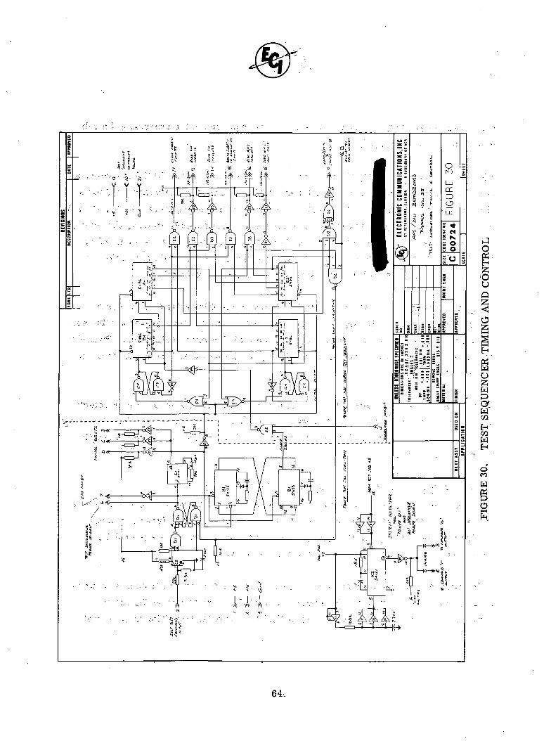
otf-H£•0uQ
O
wow
.cy.w"OT
H"CQ
^ H
oCO
W
64,
sequences are started. Further, there is no real requirement for exercising the self-test sequence "in a hurry.") ;; ,
!
After the initial reset pulse, the reset pins of the two monostables B1/B1 are released,and the clock cycles are started. Each monostable is timed for one millisecond for aclock frequency of 500 Hz. The clock then drives the timing registers B4, A4, C3 and-B3 to generate the sequencer timing. For each step of the control memory, the timing"registers clock through 200 milliseconds to create the various read pulses caused bythe stimuli injected into the system. The times and functions are detailed on theschematic and their use will be discussed with each applicable function.
The timing registers are interrupted and inhibited by the Subroutine Control Logic whichcreates its own timing. During this time, the system configuration is fixed and the sub-routine will iterate through the input commands for ISVC circuit verification. Followingeach iteration, control will return to! the Timing and Control board for continuation tothe next step.
At the. end of the test sequence, the control memory will enable gate D2, which selectsa pulse from the timing register, to reset latch D1/D1. At this time, the Test Sequencerpower supply is shut down and the initiator circuit will reset the system to the startingnormal configuration. . . • - . " " .
3.3.26 Subroutine Control Logic; Board No. 36 (Figure 31) ' - '
This board generates the timing for formulating and outputting the ISVC commands andthe read pulses required for data verification. It is enabled by the Test SequencerTiming and Control Logic at the appropriate time and it will inhibit the control logicuntil it has completed one iteration of the command set.
" ' • * " * ' !
A "subroutine enable" command is received on pin 2 which is two milliseconds in dura-tion. The state prior to this pulse is used to reset the address counter Bl and thesequence register of the Read Logic Board No. 33. The pulse transition is the'initial
65
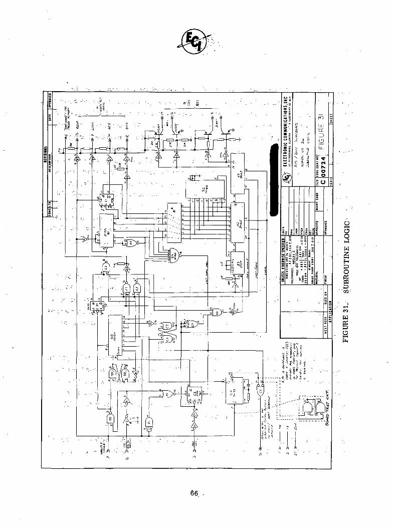
oHH
O
3w
H
O
CO,
66 -

trigger into.the r.e-triggerable.,monostable C.4 whose .output state returns an inhibit
signal to the control logic. The inhibit signal, in turn, stops the activity in the control •• :
logic which freezes the "subroutine enable" to a high and it is not permitted to clock off .
until the one-shot state returns to a high at the output of C2. With continued activity in
the subroutine logic, a retrigger is regularly provided from the Subroutine Timing.
Register D3 pin 6. Once the iterations are complete, however, gate B4 flags the 'last-
word-through' which initially returns control to the control logic and, once the remain- ;
der of the 'enable subroutine' command has been cycled through, the timing register will
cease retriggering C4 which will time out to complete the return-control cycle.' A ;second function of C4 is to yield a 'return-control'signal to the control logic should the
timing logic fail within the Subroutine Logic. This prevents lock-up in a non-functioning :
subroutine. This could happen if an ISVC circuit set were to fail while under test such <that the Subroutine Logic did not receive either clock or end-of-word information. Here,
the D3 register would cease clocking and, therefore, the required retrigger would be ;.
missed. . . . '
The timing sequence is illustrated in Figure 32 Subroutine Timing Diagram. As can be
seen from this diagram, the shift register is made to load and shift on alternate 20 micro-
second time slots as determined by the JK D4. And, during the shift cycle the address
counter is made to increment to the next word. Also, during the same word-frame time
that is used to load new data, a "read" pulse is generated such that the results of the
last word entered into the ISVC can be verified.
The discrete pulses for clocking the address counter, loading the register, retriggering
the one-shot, etc., are derived from the 8-bit Shift Register D3 which is clocked by the
system clock after it has been divided-by-two at the Cl flip-flop. This spreads these
operations out,over a period of 16 microseconds of the 20 microsecond word frame
length. .NOR gate A4 insures that the timing shift-clock is the same phase for each
frame by resetting Cl at each end-of-word.'. i
The counter B1/C1 generates the address for the ROM located at Al which is configured '•-.
for a Signetics Device 8223. However, since the APS/DIU commands were assigned

Wlo
Ou73
rtO
£H-t
HW
CMCO
W
68
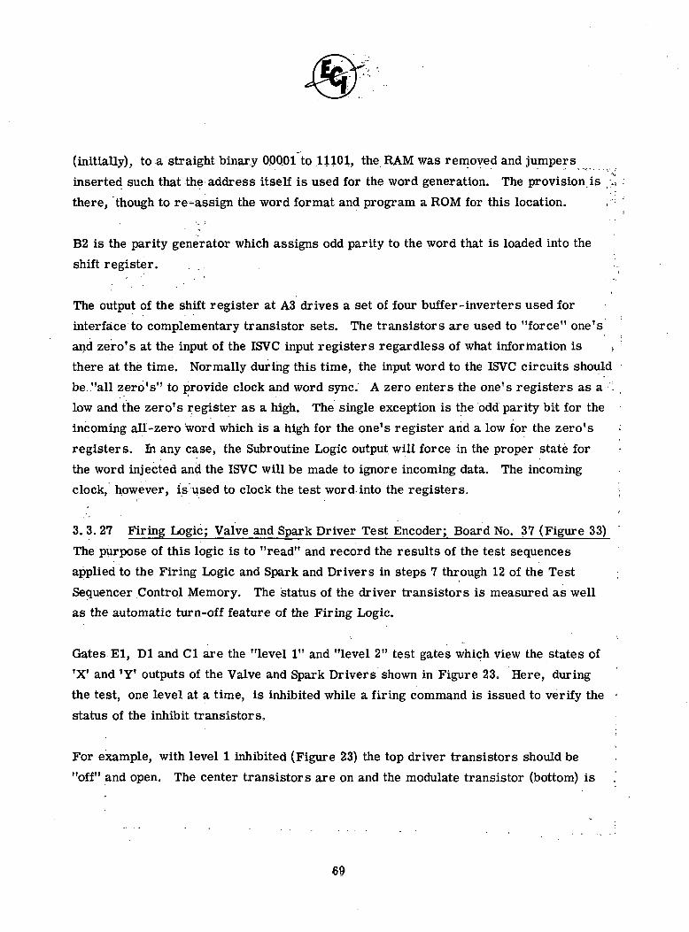
(initially), to a straight binary OOQ01 to .11101, the RAM was removed and jumpers
inserted such that the address itself is used for the word generation. The provision is _>',
there, though to re-assign the word format and program a ROM for this location. .-; '
B2 is the parity generator which assigns odd parity to the word that is loaded into the
shift register. .
The output of the shift register at A3 drives a set of four buffer-inverters used for
interface to complementary transistor sets. The transistors are used to "force" one'sand zero's at the input of the ISVC input registers regardless of what information is . :
there at the time. Normally during this time, the input word to the ISVC circuits should
be. "all zero's" to provide clock and word sync. A zero enters the one's registers as a •". .low and the zero's register as a high. The single exception is the odd parity bit for the
incoming all-zero word which is a high for the one's register and a low for the zero's ;
registers. In any case, the Subroutine Logic output will force in the proper state for
the word injected and the ISVC will be made to ignore incoming data. The incomingclock, however, is used to clock the test word into the registers. ;
3.3.27 Firing Logic; Valve and Spark Driver Test Encoder; Board No. 37 (Figure 33)
The purpose of this logic is to "read" and record the results of the test sequences
applied to the Firing Logic and Spark and Drivers in steps 7 through 12 of the Test
Sequencer Control Memory. The status of the driver transistors is measured as wellas the automatic turn-off feature of the Firing Logic.
Gates El, Dl and Cl are the "level 1" and "level 2" test gates which view the states of
'X' and 'Y' outputs of the Valve and Spark Drivers shown in Figure 23. Here, during
the test, one level at a time, is inhibited while a firing command is issued to verify the •
status of the inhibit transistors.
For example, with level 1 inhibited (Figure 23) the top driver transistors should be
"off" and open. The center transistors are on and the modulate transistor (bottom) is
69
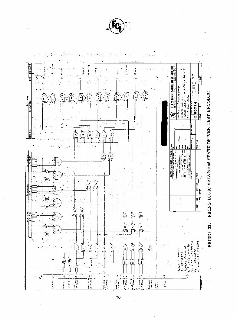
§uswHWWH
s
CO
.1W
oso
6
COCO
. w
o
TO
turned on when a firing command is programmed. During this state, the voltage ratio
between the 4. 7K resistor (located across the top transistor) and the load is measured.
At this time, the current through the load is approximately 5. 3 ma for the Valve Driver
and 5. 9 ma for the Spark Driver (both values being far below that current required to
operate the load). The voltage across the load, then, for the Valve Driver is 100 mv.The constant-current diodes located at emitters of the level 2 transistor, and the modu- •
late transistor would then both have low voltages at their inputs and their load resistors
would output logic 'zero's' if_the level 1 transistor was open and not leaky or shorted.-
A similar situation exists during level 2 inhibit except that the level 2 constant-current
diode will output sufficient current (approximately 500 /^a) to let its load resistor outputa logic high (10V). The constant-cur rent diode at the modulate-transistor would again;be current-inhibited such that the 'X' output would be a low. This condition verifies '
• -* ;
that the level 1 transistor came on and that the level 2 transistor is off and open. Both :
tests verity that the modulate-transistor is 'on1.
NOTE: The current measurements that are made with the A/D converter monitoring : ;the current of each branch of both the Valve and Spark Drivers yield a wealthof information about the drivers other than just the "on" load current. Thesedata are not recorded during the "self-test" but they could be. The variouscurrents measured during the different level-inhibits and engine firings are :essentially .indicative of the transistors off-leakages as well as the states of .the NPN controlling transistors and their sinking currents. A table of datacould be established as a troubleshooting guide to pin-point specific deteriora- ;tions different from nominal performance in the driver system. '•
With the proper states outputted from the "X" and "Y" points of the drivers, the gates !El, Dl and Cl will output a high during the read access time (Figure 33). The two level
!
tests are distinguished by the decoder logic at the left of the schematic which views the
level test in progress as well as which Firing Logic set is under test. The "read 'on' ;
pulse" at pin 13 enables a set of six gates to set a group of latches to record the testresults.
In addition, gates E3 and D3 are employed to verify the automatic turn-off feature of the
Firing Logic under test. Here, a read pulse is issued after the firing pulse should beover. K it still exists, the recording latches are set.
71
The recording latches yield the .following combined information in a two-bit code for
each Fir ing-Logic/Driver set:
0 0 level 1 & 2 & auto turn-off o.k.
0 1 level 1 test failure & turn-off o.k.
.1 0 level 2 failure & turn-off o. k.j , - •
1 .1 both level 1 & 2 failed or turn-off failed
3.3.28 ISVC and Pressure Threshold Test and Encoder Logic; Board No. 38 (Figure 34)
This board has two sets of logic on it; each recording separate tests,,
The first set, on the left of the schematic, records the status of the ISVC tests where
the input commands are cycled through the ISVC circuits with the sections powered down
in pairs.
The inputs on pins A,; B, C and D are control memory inputs indicating which ISVC
logic sets are powered. The remaining inputs are the word errors from the logic on
Board No, 33 and the; read pulse from the Subroutine Logic Board No. 36. The word
errors are registered and recorded in the latch set in accordance with the ISVC pair
that the errors occurred in. Grates Bl, B2, B2 and B2 view the latch indications and
decode, and output which ISVC circuit(s) have failed.
The logic at the right of the schematic reads and records the status of the pressure
amplifiers into a two-bit code.
Eact set of "A" amplifiers for the chamber pressure and line pressure are stimulated
with an offset voltage as is "B" and "C" in sequence. The status of their corresponding
output comparators are logically sampled first in the unstimulated mode then in the
stimulated mode to verify their performance. The information is recorded in the
following two-bit code:
72
73
•- , - •• 0 0- a l l amplifiers performing normally
0' 1 an "A" amplifier failed
10 a "B" amplifier failed
11 either an "A" amplifier and a "B" amplifier failedor a "C" amplifier failed or one each of all three
• , " ; ' . ' failed
3. 30 29'- Function Monitor Performance and Redundancy Test Encoder;Board No. 39, (Figure 35)
This logic verifies that the Function Monitors perform normally when operated with
only two of their three input supplies. Each powers a similar but separate section where
the outputs are majority-votedo In addition, this logic verifies that the automatic switch-
over feature performs as expected among the Firing Logic sets.
The logic to the left of the schematic verifies the Function Monitors performance during
steps 7, 8 and 9 of the Test Sequencer Control Memory. Here, each function monitor
has one of its sections power-disabled at the same time that the Firing Logics are
exercised.. However, because the drivers are inhibited, the sensors will feed back
"failure" information to the Function Monitors indicating that the set is inoperative.
Although the Function Monitor Control has been inhibited from controlling the Firing
Logic configuration, the outputs can be measured in response to the sensor indications.
These outputs are verified both prior to and during the "engine-on" activity by the "read
normal state" and "read sensing" pulses. The Function Monitor outputs are high prior
to stimulation and low during stimulation to indicate system failure. The information is
stored in two latches for the following two-bit code:
0 0 Function Monitor redundancy o. k.
01 a Function Monitor failed with "A" power off
, ; 10 a Function Monitor failed with "B" power off
1 1 a Function Monitor failed with "C" power off
Which Function Monitor failed is not determined but the problem area is defined by the
limited code,,
74
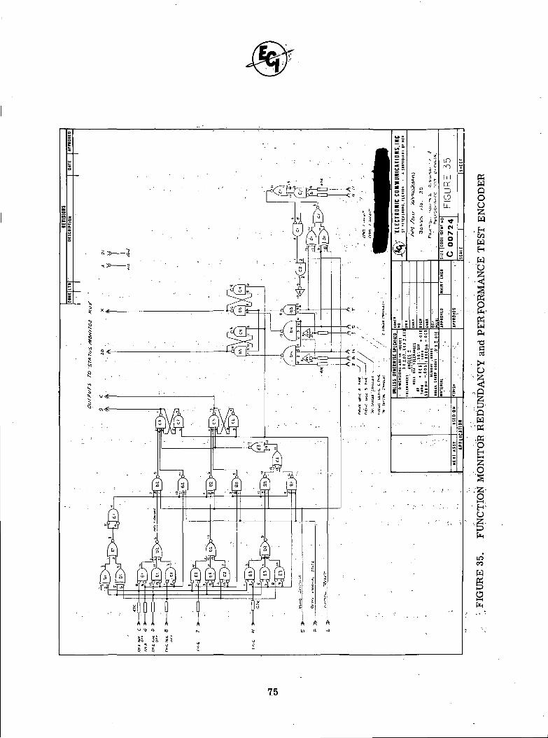
§uw
• HO)WH
W
I
T3C
u
'•aw'
O
inCO
W
75
The remaining logic on this board verifies the switchover performance of each
Function Monitor /Fir ing Logic/Power Enable/Disable set.
Since the Drivers are inhibited during the self-test, the Function Monitors are permitted
to use their "failure" information to cause the required switchover. The control memory
initiates the system into the "A" set and the engine-on command is issued. The system
should the:n switch-'over'' to the "B" set since there was no engine reaction. The engine-
on command is again issued and the system should switch once more to the "C" set. A
third cycle should witness shutdown of the "0" set.
• '< •
After the "A" 'failure' is withessed good or bad, the logic is forced into the "B" config-
uration for the next test. Again, after the "B" test good or bad, the logic is forced into
the "C" CQhfiguration for the second test. And, in turn, the "C" configuration is pro-
grammed for the last test. . The two-bit code, then, identifies the following:
, 0 Q Function Monitor and switchover performance normal
•• 0 ;: 1 system did not switch from "A" to "B"
,'; ; 1 0 system did not switch from "B" to "C"
1 1 either the switchovers from "A" to "B" and "B" to "C": : did not occur or "C" did not shut down
3.3.30 Power Interrupt Module A or B: Board No. 40 (Figure 36)
The function of these modules is to provide power-interrupt capability for both the Test
Sequencer operation as well as the. Redundancy Override commands inputting to the
s ystemi
The power interruptions are provided and controlled by latches, placed in either the
"on"iOr "off" mode, which feed open-collector buffers to interface with transistor
switched. ^Because the power interrupted is 10 V, the voltage drop in the switches is
inconsequential. '
76
77-
3.3.31 Power. Interrupt Module..C and D; Board No. 41. (Figure.37)
This Aboard is identical to Board No. 40 with the addition of another ISVC interrupt
circuit which provides power to the "D" channel.
3.3.32 Power Supplies
3. 3, 32.1 Power Supply A (Reference Figure 38)
Power Supplies A, B, and C are identical. See Table V.
Output i Voltages & Loads
Input Voltage
Ambient Temperature
PC Isolation
+ 10V, 130 ma -10V, 8 ma
+ 10V, 230 ma -10V, 30 ma
+ 15 V, 170 ma -15V, 100 ma
+ 5V, 1.5 amp
24 to 32 VDC
-55°C to 125 °CQ
> 10 ohms input to output
•••'• ! . TABLE V. ; POWER SUPPLY A(B&C) REQUIREMENTS
3.3.32.1.1 DC-to-DC Converter
The primary function of the inverter circuitry is to provide DC isolation from the
nominal 28 volt power source and to establish output voltages which are near the optimum
levels to power the associated absorptive regulators. This circuit is comprised of an
EMI filter with a re verse-polarity diode and a saturating-core inverter with associated
rectifiers and filters. The shunt diode across LI in the EMI filter prevents a large
voltage spike from being developed when the inverter core saturates and the inverter
commutates. The operating frequency of the inverter varies from 13. 7 to 17. 8 KHz for
input,voltages of 24 volts to 32 volts.
3. 3. 32.1.2 Isolated ±10 Volt Supply
A regulated supply of nominally + 10 V is generated by an absorptive type regulator
utilizing a /M.723 precision voltage regulator and a series pass element. This type of
78
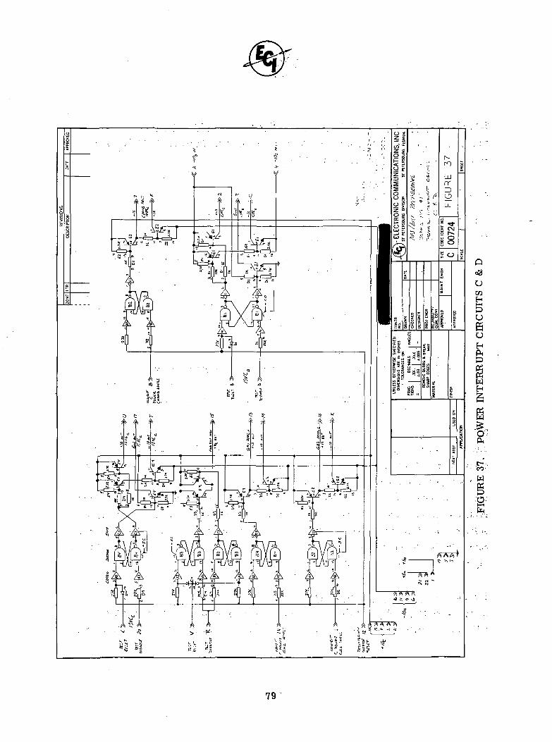
79
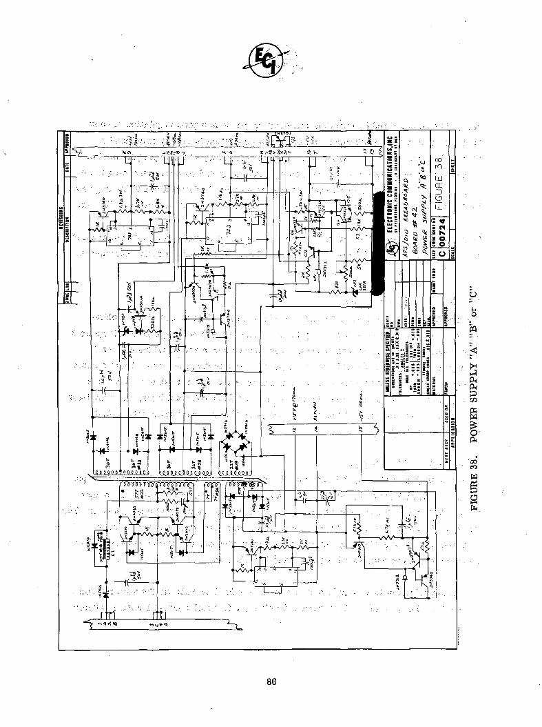
___....
f-,o.
aPH
CO
I.00CO
W
80
design is characterized by excellent transient response and good regulation against
load and input voltage variations. Short circuit protection is simply provided by ; ,
sensing the voltage drop across a small resistor (20 7 ohm) which is proportional to the
load current. When this voltage exceeds approximately 0. 6 volt corresponding to anoverload condition, the base current of the pass element is decreased and the regulator ;
limits the output current to a safe value in excess of the normal maximum of 130 ma.
Since the regulation on the -10 volt, 8 ma, supply is not critical, a simple one transistorregulator is adequate. A limiting resistor (180 ohms) protects the active components : .
from a load short. • • " • '• '
3.'3. 32.1.3 ±15 Volt Supply .:The operation of the +15 volt, 170 ma, regulator is identical to that of the isolated ;
+ 10 volt regulator. The -15 volt regulator utilizes the +15 volt regulated voltage as a
reference. This eliminates the need for a reference zener and provides automaticshutdown on the negative supply when the positive supply drops to zero. Short circuit :protection is provided by sensing the voltage across a 2,7 ohm resistor. When the
voltage exceeds the base-to-emitter breakdown of a 2N2907A transistor, the transistorconducts, thus reducing the base drive of the pass element and limiting the output,
current to a safe level. ;
3. 3.32.1.4 +5 Volt Supply
This circuit provides a regulated output of 5 volts at a load current of up to 1. 5 amps.
In the circuit of Figure 38, Q5 functions as a comparator which compares the outputvoltage to a reference voltage established by CR2 and the resistor divider network. The
output of Q5 controls the driver transistor Q2 which in turn drives the main pass ;
element, Ql. Due to the large amount of power dissipated, the main pass element is
mounted on a large heat sink fastened to the DIU chassis.
Overload protection is accomplished by sensing the load current via the voltage drop '
across R5. Because of the high current involved, a foldback current limiting scheme
81
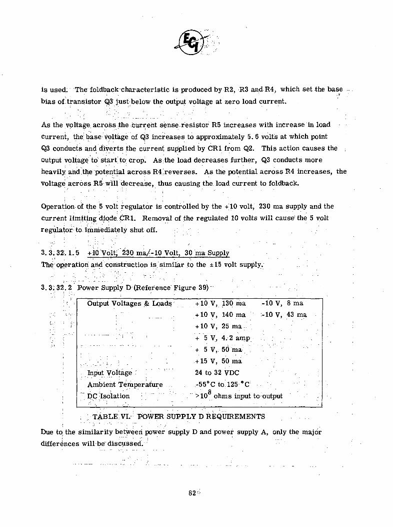
is used; The foldback characteristic is produced by R2, R3 and R4, which set the base: " • " . . ' • • , \ f
bias of'transistor (^3 just below the output voltage at zero load current.
As the voltage across the current sense resistor R5 increases with increase in load
current, the base voltage of Q3 increases to approximately 5. 6 volts at which point
Q3 conducts and diverts the current supplied by CR1 from Q2. This action causes the ;
output voltage to start'to crop. As:the load decreases further, Q3 conducts more
heavily and.the potential across R4'reverses. As the potential across R4 increases, the
voltage across R5 will decrease, thus causing the load current to foldback.
Operation of the 5 volt regulator is controlled by the +10 volt, 230 ma supply and the
current limiting diode CR1. Removal of the regulated 10 volts will cause the 5 volt
regulator to immediately shut off. r :
3.3:32.1.5 +10:Volt; 230 ma/-10 Volt, 30 ma Supply,. i ' . : . — - r— ~~;— ., . ...
The/operation arid construction is similar to the ±15 volt supply. ,
3. 3i 32. 2 Power Supply D (Reference Figure 39)
Output Voltages & Loads
Input Voltage : :
Ambient Temperature
DC Isolation. ;
+ 10 V, 130 ma
+ 10 V, 140 ma
+ 10 V, 25 ma
+ 5 V, 4.2 amp
+ 5 V, 50 ma ',
+ 15 V, 50 ma
24 to 32 VDC
-55°Ctol25°C
. >10 ohms input to output
-10 V, 8 ma
:-10 V, 43 ma
: TABLE;VL POWER SUPPLY D REQUIREMENTS
Due to, the similarity between power supply D and power supply A, only the major
differences will be discussed.
82-
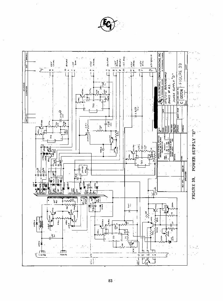
83
3.3.32.2.1 +10 Volt, 25 ma Supply Shutoff
The operation of the +10 volt supply is controlled by a logic level supplied to pin 5 onthe emitter of the 2N2222A transistor. A low level ties the emitter lead to ground and
allows the transistor to conduct. This in turn shuts off the regulator. A high level or
an open will allow the regulator to function properly. The +10 V regulator in turn
controls the 5V, 4. 2 amp supply.
/ • • ' ' • • • • ' , - " • ' •3 . 3 . 3 2 . 2 . 2 + 5 Volt, 50i ma SupplySince the current requirement on this supply is low, a LM109 was chosen to provide theregulated 5 volts. Current limiting is included to limit the peak output current to a safevalue. In addition, thermal shutdown is provided to keep the 1C from overheating.
3.4' TEST SET.' / > . ' • . ' " " , . . '.. - • ' • - ' ' ' . '.
3.4.1 Functional Description ; .
Figure 40 describes the front panel configuration of the APS/DIU Test Set which is alsoconfigured to operate and test the Actuator Interface Digital Interface Unit breadboard
presently under construction for NASA.
The Test Set is comprised of two panels; a control panel and a display panel. The
control panel sources information to be sent to the APS/DIU as a simulation of the Data
Terminal/Data Bus function. The display panel utilizes the outputs of the APS/DIU todisplay the spark ;and valve functions, the'Status Monitor output words, the EmergencyShutoff Monitor status plus various controls to normalize, fail or input external bridgeresistances for .the system pressure strain gauges. The remaining displays are
Actuator Interface Unit functions which are not to be included in this report.
3.4.1.1 Control Panel
The Control Panel incorporates toggle switches to manually program the Supervisory
Word used to feed the APS/DIU when" the "MANUAL COMMAND/ENGINE ON-OFF"
switch is in the "MANUAL COMMAND" position. The toggle to the right of the Supervisory
84.
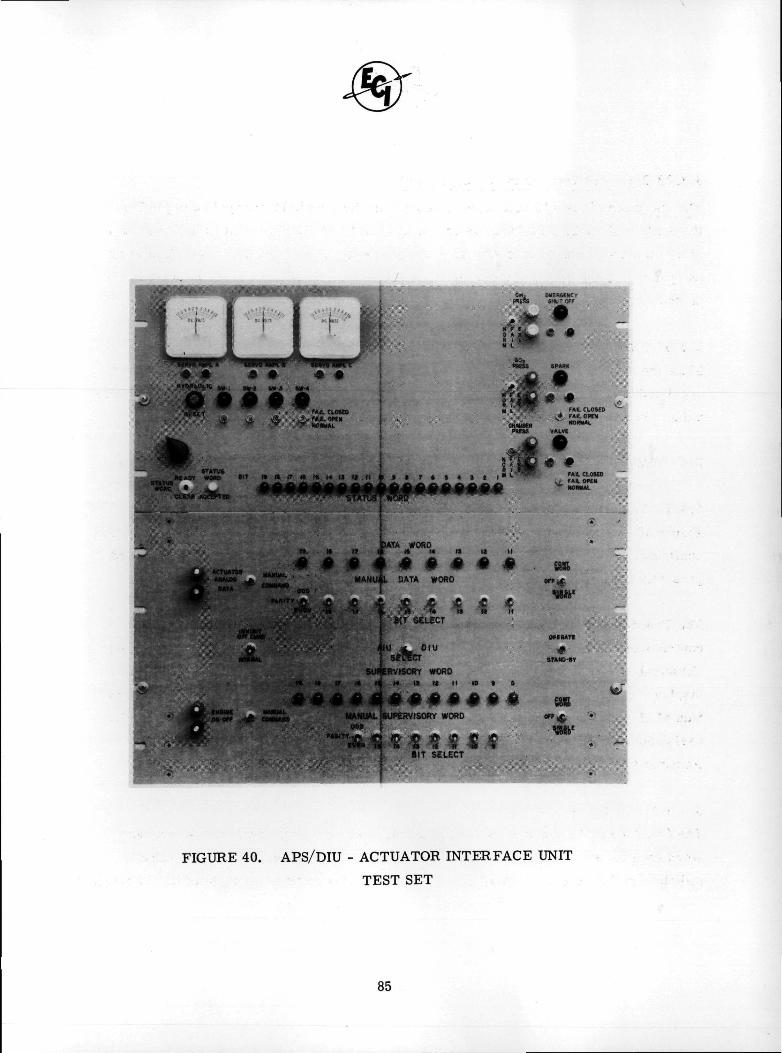
MANUit OATA WORD
DAW WORDf a tt a a it
ItT SELECT
hu « eiuI sllfer
sufpmnsoRY WORD
MAI«1*L {SUPERVISORY WORD
u It H "*BIT SELECT
OMIMTI
"*'STANO-8Y
88
FIGURE 40. APS/DIU - ACTUATOR INTERFACE UNIT
TEST SET
85
WorcUet labeled ,''CONTXWORD:-OFF: SINGLE WQRD" sets the status of the output
information.^- For, instance, in the "OFF" position, the Supervisory Word is a continu- .
ous 'all-zero' wprd with; odd or even parity programmable with the parity switch at
bit.16.: The, remaining switches do not offer any .bit control during this condition. When
the toggle is placed in the "CONT WORD",position, the Supervisory Word outputted is
that which is programmed (including the parity selected) and the word will exist within
each 20 microsecond word frame produced. When the "SINGLE WORD" position is
toggled into this momentary position, a single word is issued at the supervisory output
in accordance with .the program set. After the single word outputs, the Test Set will
then continue,.to output.the/all-zero' word as before. .
Now, when the MANUAL COMMAND/ENGINE ON-OFF switch is in the ENGINE ON-OFF
position, manual,control is inhibited,except that either CONT WORD or OFF is
programmed.,;In CONT WORD, the output word is controlled by the ENGINE ON-OFF
input. Here,r<a square-wave generator is used for a singnal source where the frequency
may be^set for repetitious engine,.firings ie., 1 Hz. In.addition, when operating in this
ENGINE ON-OFF,mode, the "off" command may be inhibited by the switch provided.
The OPERATE/STANDBY switch inhibits all test set functions in the STANDBY mode
such that it will output nothing. , , ...
3.4.1.2., Display, Panel . . , . . .
The panel essentially "closes-the-loop" for the APS/DIU by displaying the outputs avail-
able. The EMERGENCY SHUTOFF lamp is illuminated when a Emergency Shutoff
Command has-been issued on the Control Panel or when the system senses and generates
its.own ESO condition. ,,The pin.jacks provided permit metering the voltage available
from the APS/DIU ESO driver. The SPARK lamp illuminates when the Spark Driver is
activated within the APS/DIU as does the VALVE lamp. Both the Spark and Valve inputs
to the Test Set are appropriately loaded to simulate the system load; 25 ohms for the
Spark Driver:and^560 ohms for the Valve Driver. ._ Again, pin jacks are provided to
measure both the voltage of the,drivers as well as the timing. Two additional toggles
86
are provided to simulate "failure" modes of the Valve and Spark terminations. The
' Valve may be 'failed' open or closed meaning that the fuel line is closed or opened
respectively. The Spark has the same failure provisions of the Display Panel except
the APS/DIU does not receive feedback from the Spark High Voltage Supply in the system
and, therefore, the APS/DIU will not react to a Spark failure except if its internal
driver fails.
Three additional sets of controls are available specifically for the GH2, GO2 and
CHAMBER PRESSURE indications to the APS/DIU. Each has an associated toggle
switch such that the transducer may be "NORMAL", "FAILED" or simulated "EXT"
(externally).
The"N<DRMAL" position provides a resistance (511 ohms) for the bridge -inputs of the
APS/DIU Strain Gauge Amplifiers. This value remains fixed during engine-fir ings for
both the GH2 and GO2 line pressures. The resistor is altered, however, for theCHAMBER PRESSURE during engine firings to simulate the generation of chamber
pressure. This is done with a relay which adds approximately 12 ohms to the 511 ohmsin the bridge load.
The"FAIL" position of these switches alters the bridge such that the amplifiers willcross the failure-detected threshold of approximately 1 volt. In the CHAMBER PRESSUREset, the failure eliminates the capability to simulate 'chamber pressure' during engine
firing by keeping the bridge resistance fixed. •''
The "EXT" position allows utilizing an external decade resistance box for substitution
into the bridge. Here, the amplifiers and A/D Converters monitoring these values may
be calibrated.
3.4.2 Electrical Design
The modules discussed for the Test Set are assembled on boards similar to those used
in the APS/DIU breadboard. All logic components are TTL 7400 devices or comparable
87
equivalents. The boards are .wirerwrapped and the power is supplied by external
laboratory bench supplies. •L * " ( - '
3. 4. 2.1 Supervisory Word Generator (Figure 41)
This board generates the specific commands to be entered into the word stream feeding
the APS/DIU ISVC/circuits.
The switches shown,at,the left of the schematic are used to program the significant,..; ! V . ' • ' ! . ; •
bits into the Supervisory Word. This information is multiplexed-selected with theencoded ."engine-on" and "engine-off" commands developed automatically by the logic atthe lower-left which is feclby a squarewave generator. The ENGINE ON-OFF/MANUAL
COMMAND switch controls which data is selected.
The data' is leaded into a 20-bit serial register comprised of Fairchild 9300's and is
shifted put through <a single Polar RZ modulator (75325) to drive the four lines to theAPS/DIUo During this shift cycle, the outputted data is detected by a comparator andre-cycled back through the shift register. At the end of each 20-bit 20 microsecond word
frame, the information is parallel-shifted into a set of quad "D" storage elements which
drive display lamps. This mechanism provides assurance by the lamps that the wordthat was programmed was outputted through the Polar RZ modulator. The data selected .
to load into the registers is pre-empted by the 'cycle-control' which disables.the multi-- •('
plexer arid enters all zero's into the registers.•
3.4. 2. 2 Timing Logic (Figure 42)
This logic develops the timing and control for the Supervisory Word and the Data Word
(employed in the Actuator Interface breadboards).
The logic is configured to generate 20-bit consecutive word frames plus the data frames
which are in sync with the Supervisory Word. Further, the register load pulses, Super-visory Cycle Control, A/D Clock (A0L function), register shift pulses and Polar RZ
clock pulses are developed and outputted.
88
-";c\ o~- J- c jb *X'c (fib of o 0 jb t\ o o \0 - o o' o .o•^ ^1 S y y 6 0 ., .0
H, U I,, ^ L,,. L,, J L,,, .;: U^30. j
jU "
Ou.
' rt
tfO
o.a
I
w
60
•T—I
W
89
u
o
CM•"*lw
90
The counters located at C4 and X4 count the 1 MHz clock pulses and the one-shots at
D4 generate the reset function after a 20-bit frame has been accumulated. The logic at
the top and at the bottom of the schematic is nearly identical to develop the controls of
"Continuous Word", "Single Word" or "all-zero" words (off) for both the Supervisory
and Data sections.
Figure 43 describes the timing and signals generated.
3.4.2.3 Display Panel Status Monitor (Figure 44)
The function of this circuit is to accept single words from the APS/DIU (or A,,I.) and
store and display the word information in 19 bits.
The data is received on four pair (schematic left) and line-selected by a rotary switch.
The line is then transformer coupled into a pair of comparators used as line receivers
to recover the clock from the data. The data is outputted from comparator El and is
fed to the shift register comprised of Fairchild 9300's. The two one-shots at Al are
used to develop the register shift clock (125 nsec) and the "end-of-word" pulse (1. 25 jjsec).
The end-of-word pulse loads the storage elements which feeds the lamp drivers.
A latch is shown (upper left), at location X2, which is used to recognize and drive a
lamp indicating that a 19-bit word has been received and accepted. The purpose of this
added lamp is to inform the operator that an "all zero" word has been received as
opposed to the Test Set receiving an "all-zero" word without any indications of activity.
A reset switch is provided to clear this latch.
3.4.2.4 Display Panel Control Logic (Figure 45)
This board serves two functions:
(1) provide simulated hydraulic switching to close-the-loop; on the Actuator Interface Breadboard, and
(2) provide both a load and display for the APS/DIU as well :as pressure sensor simulation.
91
Ou•ortO
92;.
§
H<HOT
JH
OTt—ip
93
: l—i?
. i 'V . •- '-HP- - I - - .
O»— io2
-O.UJw£2
Pnra-
in
W
P
94

The Ac I» Uo portion of this board will not be discussed in this report.
The right side of the schematic details the hardware used exclusively for the APS/DIU,
The Valve Drive is shown inputted on pins L and M of connector 3 and driving a relay B2.The load presented by this relay is 40 to 50 ma so no additional load resistor is
included. The contacts of this relay are used to feed through the "failure" switch SW11.
This switch is tied to the valve lamp as well as relay B4. A pair of contacts are brought
out from B4 to simulate the "Valve Switch" requirements of the APS/DIIL In addition,another pair of contacts are placed across a 12 ohm resistor such that the resistance
increases during valve activity.
The Spark input also drives a relay but, in addition, a 25 ohm resistor is across therelay to raise the driver load current to 1 amp. The Emergency Shutoff Monitor is also
fed to a relay. The relays for both the Spark and ESO drivers are used to illuminatelamps.
A contributing asset derived from the use of relays (with diode protection) is the inherentdelay in turning them on and off. This delay somewhat simulates the delays that may
be experienced in driving the actual valves.
3.4.2.5 Actuator Interface Breadboard Test Set Modules
The remainder of the Test Set functional modules are utilized exclusively for testing the
Actuator Interface Breadboard(s) and will not be discussed in this report,, They are
included only for information purposes.
Figure 46: Clock Generator and A/D Converter
Figure 47: A. L U. Data Generator
Not Included: Analog Mathematical Model
95
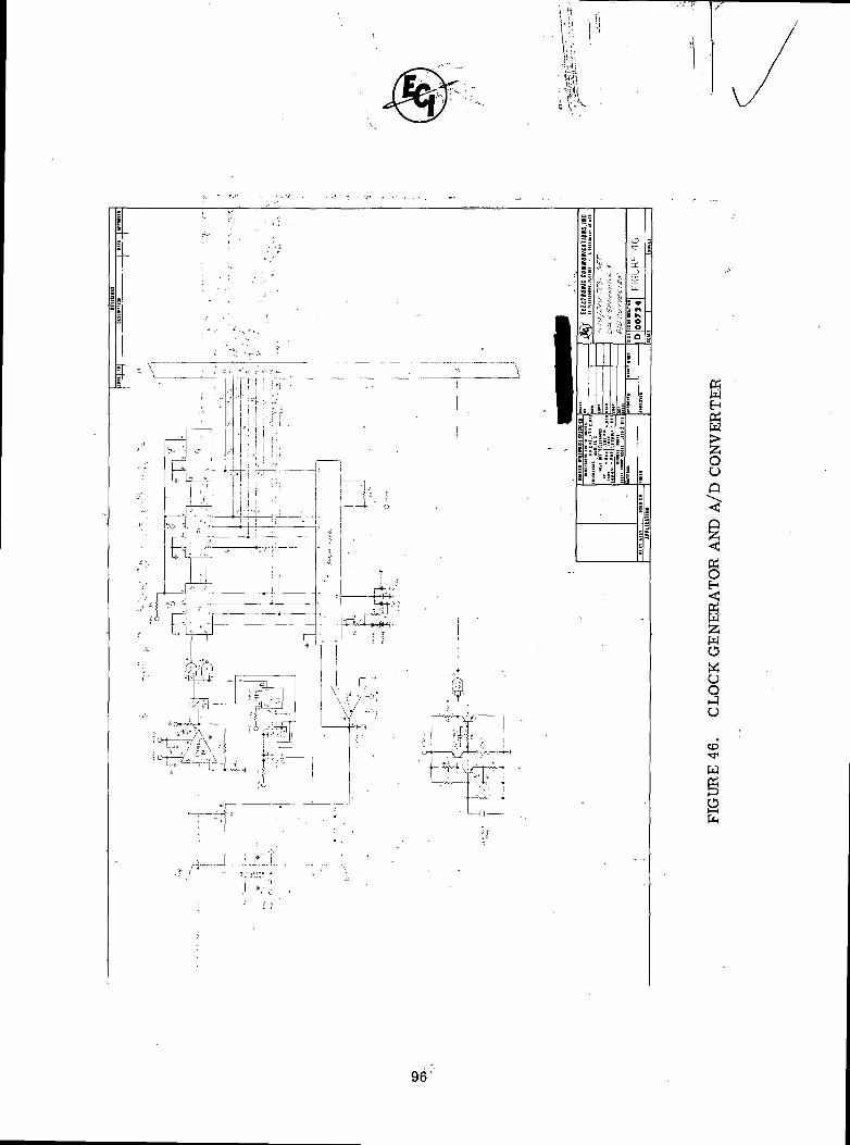
Is i i i
KWEH
55OOP
<?
§H55WO«u
CD
96
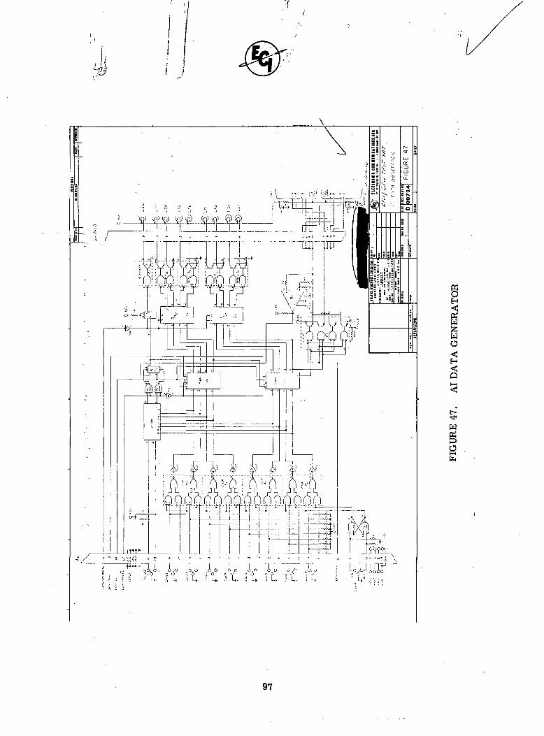
I i
w.. i'(ni (f) (QJ to) tp> fa) (ci) © (p)
. ,. .. . ,
?^teIU
DU
s «• «
iu
wo
w
97
4.0 CONCLUSIONS-AND RECOMMENDATIONS - ,-i i - - ' '' -i . . . *'
• - . „"'£ '. ^ *• :-* *f. , ' ••' - f • i-, * , ' • < : t * . * , * - . , . '
4.1 SYSTEM PERFORMANCE . • • • - • : , ' ,
The breadboard system generally performed as was originally intended in the proposal
concept with few design deviations. Because the design was oriented toward a "final
product" in LSI format, the designs of several areas became more complex than that
which would have resulted from a "minimum hardware" approach. Some design areas
are merely 'go-as-is1 circuits; that is, the implementation into LSI is virtually an
immediate conversion from the operational schematics. Other areas require modifica-tion of minor changes in concept for more efficient implementation; this was proven by
- j C • • - - , , - , . ' .< . - -
the breadboard effort, ' ;
-'••i t . , * . - - - \ • ; , • -• '• >
Making this breadboard perform yielded several ideas. First, it proved that the dual-
failure immunity concept is complex;' Yet it; is hot so complex to make if impractical toimplement. Even to the extent that it was implemented in the APS/DIU where it
manages'its own redundancy. '" Second; the breadboard demonstrated two types of redun-dancy philosophies; four-wide and three-wide. Here, the four-wide circuits "perform
identically and in parallel as in the'ISVC circuits. Failure immunity is achieved by acomplex of inter-voters to compare-out the errors. The three-wide operates singly
•f ^ - i • \ -• -•• . - , *and individually.' A single function, as in the Firing Logic set, implements sufficientcircuitry to'-determine its own validity. And,"'when it fails, it powers up an identical
backup to perform thV same function.
Both techniques have'their merit; both performed well. 'Both required added hardware;
both are difficult to test. Yet, together they complement the requirements of functional
performance, minimum density and minimum power requirements.
4.2 DESIGN CONSIDERATIONS
"As proven out in the breadboard system, the circuit designs operate. However, some•••<• C'-'- ' * ' •-•• V*1* • ' • ' , - • •
circuits are basically inadequate or over-designed and; although this has been recognized,
no additional time wlis consumed ttf re -arrange these designs.
98

It is the function of a breadboard program to point out deficiencies and, unless the ;
problem is major, they usually need not be corrected as long as the 'fix' is operational
and the problem is clearly identified. .
These areas will be discussed in this section.
4.2.1 Line Receiver/Photo-Isolator Interface Circuit (Reference Figure 11)
The function of this circuit is to provide an isolated interface between the input lines and
the APS/DIU processing circuits. The purpose of designing a photo-isolator interface
was that, in microTinin technology, it could conceivably be packaged in less volumethan a transformer plus its related circuitry. This may still be true; however, thecircuit that resulted during the breadboard program became necessarily complex such
that it would perform over temperature, and, its power requirements are high. TheMCD-4 photo-isolator diode works over temperature provided that it is driven hard
(160 ma each) and the recovery circuits required to re-establish the data are complex ,.
and consume considerable power. Consequently, the circuit is considered too complexfor the function that it performs; and, since it is a "power-hog" it is doubtful that itcould be efficiently micro-miniaturized considering the heat that has to be removed.
Conclusively, the photo-isolator technique should be shelved until more efficient devicesare available and the circuit should be replaced with a pulse transformer coupler, as
shown in Figure 48. The volume of the transformer can be small and its associated
circuitry can be hybridized. The end volume consumed would probably be less thanthat required to produce the photo-isolated unit plus the power supply required tosupport it. . ,
4.2.2 Power Enable/Disable Logic (Reference Figures 16, 17 and 18)
The logic in these functions is triplex/majority-voted to an output set of quad transistors
and parallel transistors used as switches to 'turn-on' or 'ground' the power to the FiringLogic. This circuit can be considerably simplified using a set of buffer/drivers to
control the power switching instead of transistors. The power requirements of the
Firing Logic is considerably less than is presently deliverable.
99
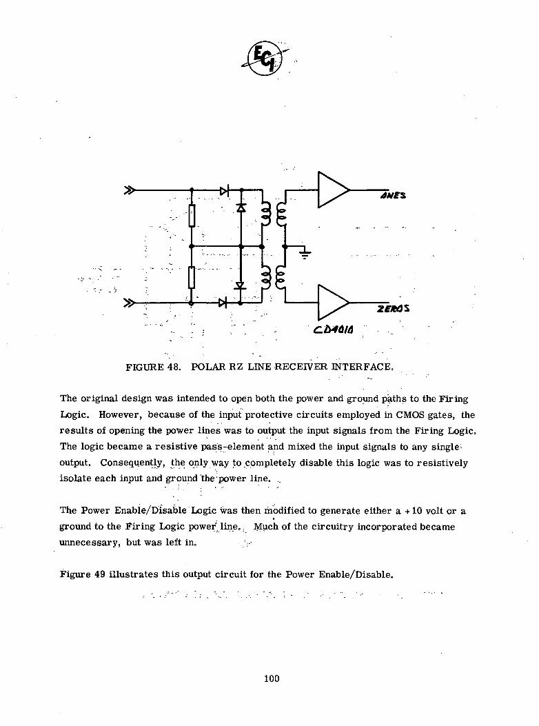
4A/ES.
FIGURE 48. POLAR RZ LINE RECEIVER INTERFACE.
The original design was intended to open both the power and ground paths to the Firing
Logic. However, because of the input protective circuits employed in CMOS gates, theresults of opening the power lines was to output the input signals from the Firing Logic.
The logic became a resistive pass-element and mixed the input signals to any single-
output. Consequently, the only way to completely disable this logic was to resistivelyisolate each input and ground "the'power line.
The Power Enable/Disable Logic was then modified to generate either a +10 volt or aground to the Firing Logic power^ line,,; Much of the circuitry incorporated became
unnecessary, but was left in. y
Figure 49 illustrates this output circuit for the Power Enable/Disable.
100
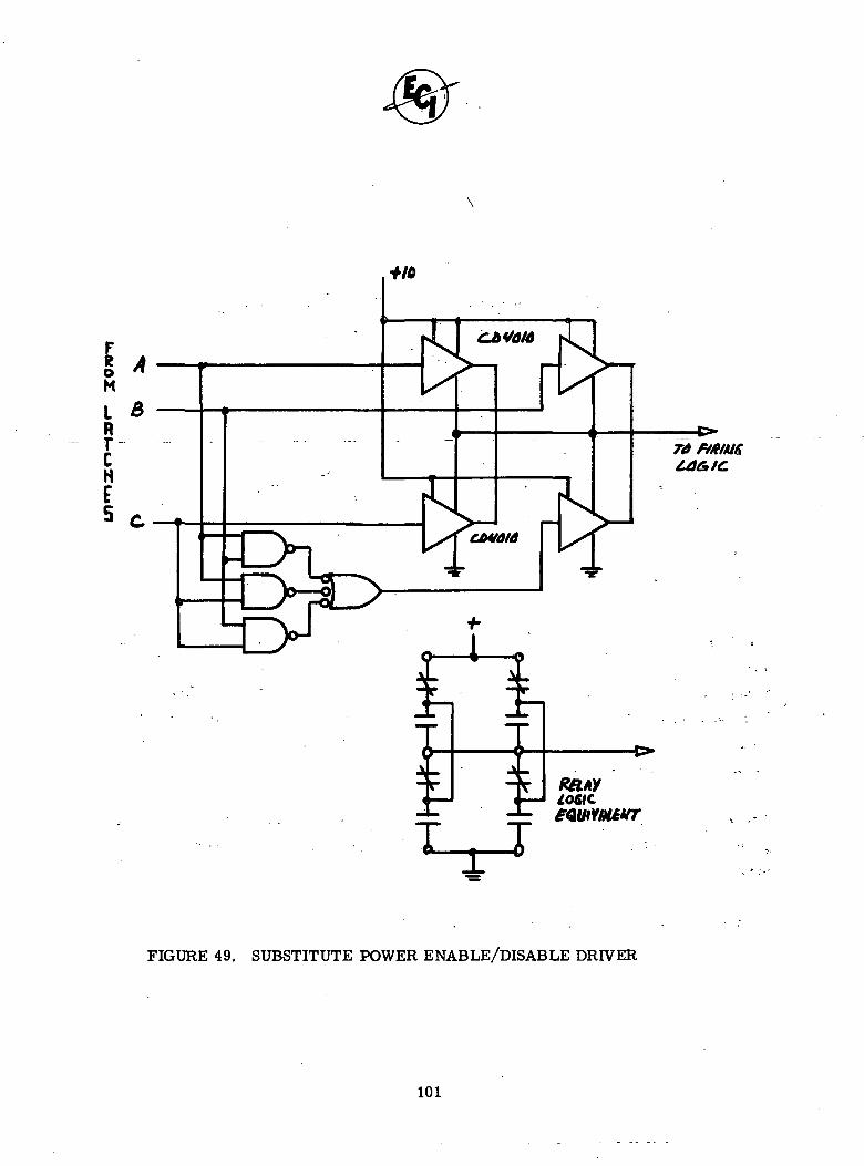
KflAYtoeic
FIGURE 49. SUBSTITUTE POWER ENABLE/DISABLE DRIVER
101

4.2.3 Test Sequencer;.-(Reference Figures 28 through 35) . .
4.2. 3,1 TTL versus CMOS'Implementation . -.«
The circuits designed and fabricated for the Test Sequencer were done, in part in TTL
as opposed to CMOS. During the design effort, several areas had to remain flexible so
that during system test the functions of the Test Sequencer could'easily be updated if "
necessary. Consequently, TTL was employed in the timing and control sections because
of its convenience and availability. .
In the final configuration, the Test Sequencer would be implemented in CMOS/LSI
because its design has been virtually finalized. Again, the breadboard proved out the ,
feasibility of the technique, and the direction has been defined-for the final package.
4. 2; 3. 2 'Philosophy of .Data.Formulation
Presently,^ the Test Sequencer is configured to output an "all-zero" word if all functions
perform correctly or a pattern of one's, some of which are 2-bit codes identifying
probable if not specific, failed area. Two significant changes are recommended in
this area: " ' . . « ' . . ; ' ,-„• , . , . : • ' . ' - •
--• >(1) At the initiation.of the 'self-test' a reset pulse is issued to ;..,,.- ..-, . n fix the re cor ding, latches to a 'zero' state and then as failed
information is collected," it is used to set the latches to the v
* -• ^ j ? • .- 'one'state. After this scheme had been-implemented, .it . ,., . became obvious that this initiation method and collection .
"' "l ' " "'"'" method is inverse of the ideal process. That is, the reset• I .. ' . " •"-•:.' pulse should fix the latches to an all 'one' state (the failed .
state) and as good information is collected, the latches areset to the 'zero' state. Here, it takes correct logical activity
, , ,, to recognize "good" performance rather than inactivity imply-, ,,.,ing "good" operation and activity recognizing "failed" data.
An examination of the system shows several areas where aTest Sequencer gate could fail and the resultant outputted infor-mation would indicate that the tested operation was valid. TheTest Sequencer operation would not be suspect until the system
.;• -• - - itself did not perform as well as the Test Sequencer indicated -it should.
102
(2) Another area which should be considered for designalteration is the bit scheme used to indicate the testresults. Presently, the outputted 16-bit word is adirect readout of several tests; some single bitsassigned for "go-no" of a specific section or a two-bit code indicating such things as "A is bad; B isbad, or both A and B are bad, or C is bad. " Thesetwo-bit schemes depend somewhat on the probabilityof catastrophy and are really insufficient as a measureof the system performance,, It is recommended,therefore, that an encoding scheme be devised to takeadvantage of the 2*6 possible combinations that couldexist for the 'self-test' report.
4. 2. 3, 3 Test Sequencer Tests 13 through 15
The intent of these three tests was to validate the automatic switch-over capability from
Firing Logic "A" to "B" to "C" and then off. The sequence would depend on the Function
Monitors to recognize that the engine was not responding to the Firing Logic commands
(they were inhibited) and would therefore shut down their associated set and cause turn- .
on of the backup.
Once the system had been assembled and operating, it was recognized that this function
did not work as a process of the Test Sequencer. The control memory function of the
Test Sequencer has "hard control" of the various APS/DIU functions including the
Power Enable/Disable Logics as it sequences through the various tests. That is, it
will force a circuit on or force it off and it will hold that given state until the reverse is
required. This hard-control has to be released during tests 13 through 15 but maintained
for the earlier tests. For instance, at the beginning of test 13, Logic Set "A" has to be
turned on such that the Function Monitor can turn it off when it recognizes the 'failure.'
The Control Memory, however, holds it 'on' continually and therefore the Function
Monitor 'turnoff activity is not recognized nor is the backup logic "B" turned 'on'
since it too is held off by the memory.
Because this problem emerged at the time that the unit was due to be delivered to NASA,
a redesign was not undertaken to fix this test although the method for doing so is
103
recognized and the modifications will be added if NASA requires it in the breadboard.
First, two "test^enable",and test disable!1 inputs have to be configured to each of the .
Power Enable/Disable boards "A", "B" and. "C". One of these sets would be used for
the 'hard-control';requirements and the other would be considered 'soft-control' where
the required configuration is capacitively pulsed at the beginning of the test and control
released throughout the test. Here, for instance, Power Enable/Disable "A" would be
pulsed "on" at the beginning of test 13 prior to the issuance of the "engine-on" command.
Power.Enable/Disable sets "B^ and "C" would be pulsed "off" at this same time. Then
the logics would be free to act among themselves and the results measured. .-At the
beginning of test 14 "B." would be pulsed 'on and "A" and "G"-would be pulsed "off:
prior to the !'engine-on" command. Again, the logics would be free to act among
themselves and the results measured. A similar process would be exercised for
test 15.
4..2.S/4 :Power Supplies and Power Consumption
The system breadboard consumes approximately sixty watts in its present configuration
which is considerably higher than.necessary. The power supplies are designed to supply
this energy for the breadboard. In the final configuration, with all circuits LSI and/or
hybridized and with the TTL elements minimized, it is estimated that the power require-
'*ments:wili-be less than 10 watts maximum. This means a considerable reduction in the
volume requirements for the power supplies (although the same design philosophy will .
be followed) and less-heat to remove. .• -
Theicircuits adjusted for -reduced power would be the Line Receiver (transformer ,
coupling instead of photo-isolation), the Power Enable/Disable Logic, the Test
Sequencer (CMOS instead of TTL)j and the Power Interrupt circuits which are designed
to switch heavier loads than will be required.
104
4.3 LSI IMPLEMENTATION
The next step in the APS/DIU development would be the manufacture of LSI prototype
models using CMOS/LSI and hybrid techniques for the non-digital circuitry. Because
the chip manufacturing technique yields multiple chips for each single run, the prototype
fabrication would, in fact, yield approximately 20 models for the cost of one.
4.3.1 Implementation Procedures
The system would first be partitioned into areas that operate from a common supply
with a minimum I/O count plus maximum device count. Specifications would be rigidly
defined for the function(s) such that the logic diagram may be computer verified for
functional validity. At this time, revisions may be programmed to improve response,
propagation delay, etc., and this also will be computer-verified as well as generate
updates in the logic diagrams. • - . . - ' . .
Once the functional diagrams have been idealized, the design is ready for layout. Here,
the "cells" are compiled from the library of devices presently available to generate the
functions required. Computer layout may be used exclusively or it may be complemented
with additional hand layout to maximize the density if the particular chip design is ,
crowded.
Once the layout is complete, the photo artwork is generated to create the masks required.
Then the wafers are exposed and the processes of diffusion, oxidation and metalization
are performed as required. Several tests are performed on the wafers as they are
produced to verify their operational characteristics and then they are packaged in multi-
pin flat packs or just dices for chip-and-wire bonding to other devices on a-substrate. f;
The processes briefly outlined here are shown in Figure 50, in block diagram form. . •
4.3.2 jliSI Implementation Program Requirements
A typical turn-around time for chip production is approximately 60 days, given 30 days
for design and thirty days for prototype production. However, several tasks must be
105
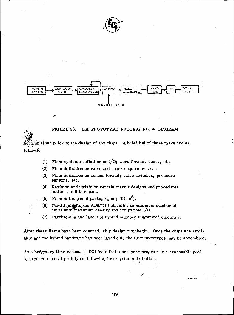
JTEST
MANUAL AIDE
FIGURE 50. LSI PROTOTYPE PROCESS FLOW DIAGRAM
.accomplished prior to the design of any chips. A brief list of these tasks are as
follows:
(1) Firm systems definition on I/O; word format, codes, etc.
(2) Firm definition on valve and spark requirements.
(3) Firm definition on sensor format; valve switches, pressuresensors, etc.
(4) Revision and update on certain circuit designs and proceduresoutlined in this report.
.- (5) Firm definition of package goal; (64 in^)0
(6) Partitionm^ofjrthe APS/DIU circuitry to minimum number ofchips with' maximum density and compatible I/O.
(7) Partitioning and layout of hybrid micro-miniaturized circuitry.
After these items have been covered, chip design may begin. Qnce,the chips are avail-
able arid the hybrid hardware has been layed out, the first prototypes may be assembled,,
As a budgetary time estimate, ECI feels that a one-year program is a reasonable goal
to produce several prototypes following firm systems definition.
106
Related Documents


