Calhoun: The NPS Institutional Archive DSpace Repository Theses and Dissertations 1. Thesis and Dissertation Collection, all items 2001-03 Feasibility analysis and design of a fault tolerant computing system: a TMR microprocessor system design of 64-Bit COTS microproces Eken, Huseyin Baha http://hdl.handle.net/10945/10857 This publication is a work of the U.S. Government as defined in Title 17, United States Code, Section 101. Copyright protection is not available for this work in the United States. Downloaded from NPS Archive: Calhoun

Welcome message from author
This document is posted to help you gain knowledge. Please leave a comment to let me know what you think about it! Share it to your friends and learn new things together.
Transcript
Calhoun: The NPS Institutional ArchiveDSpace Repository
Theses and Dissertations 1. Thesis and Dissertation Collection, all items
2001-03
Feasibility analysis and design of a faulttolerant computing system: a TMRmicroprocessor system design of 64-Bit COTS microprocessors
Eken, Huseyin Baha
http://hdl.handle.net/10945/10857
This publication is a work of the U.S. Government as defined in Title 17, UnitedStates Code, Section 101. Copyright protection is not available for this work in theUnited States.
Downloaded from NPS Archive: Calhoun

NAVAL POSTGRADUATE SCHOOL Monterey, California
THESIS
FEASIBILITY ANALYSIS AND DESIGN OF A FAULT TOLERANT COMPUTING SYSTEM:
A TMR MICROPROCESSOR SYSTEM DESIGN OF 64-BIT COTS MICROPROCESSORS
by
Huseyin Baha Eken
March 2001
Thesis Co-advisors: Alan A. Ross Herschel H. Loomis
Approved for public release; distribution is unlimited.
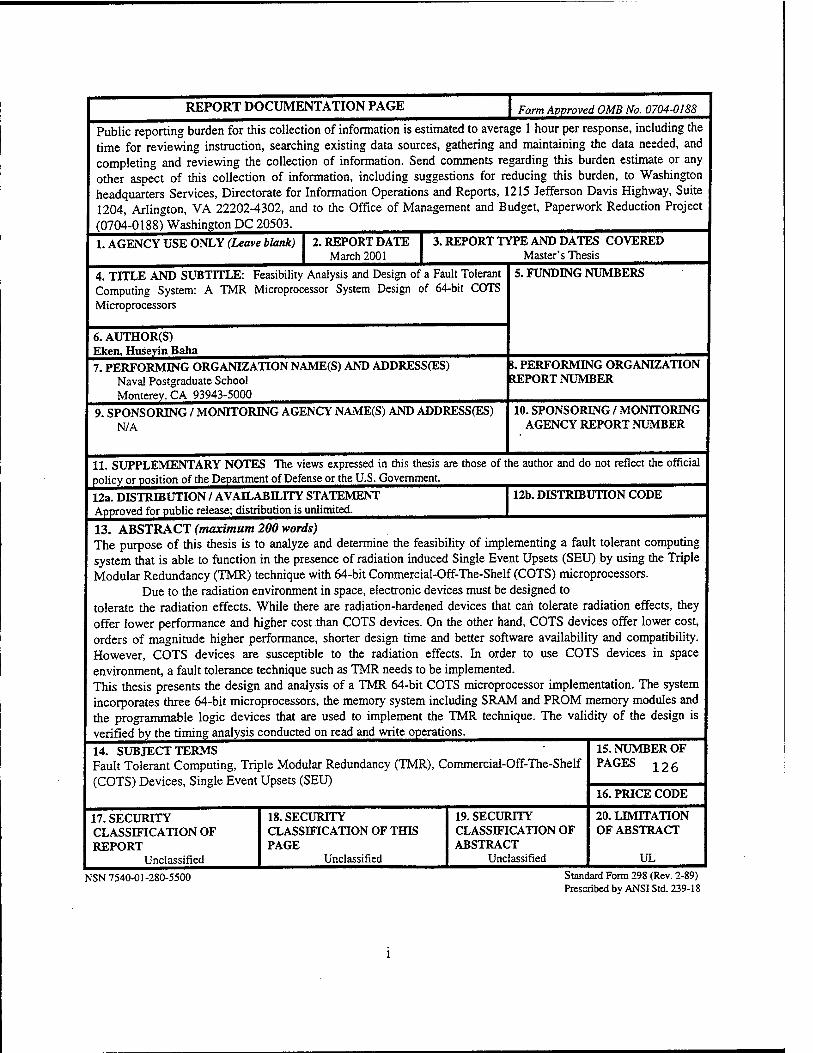
REPORT DOCUMENTATION PAGE Farm Approved OMB No. 0704-0188
Public reporting burden for this collection of information is estimated to average 1 hour per response, including the time for reviewing instruction, searching existing data sources, gathering and maintaining the data needed, and completing and reviewing the collection of information. Send comments regarding this burden estimate or any other aspect of this collection of information, including suggestions for reducing this burden, to Washington headquarters Services, Directorate for Information Operations and Reports, 1215 Jefferson Davis Highway, Suite 1204, Arlington, VA 22202-4302, and to the Office of Management and Budget, Paperwork Reduction Project (0704-0188) Washington DC 20503. 1. AGENCY USE ONLY (Leave blank) 2. REPORT DATE
March 2001 3. REPORT TYPE AND DATES COVERED
Master's Thesis
4. TITLE AND SUBTITLE: Feasibility Analysis and Design of a Fault Tolerant Computing System: A TMR Microprocessor System Design of 64-bit COTS Microprocessors
6. AUTHOR(S) Eken, Huseyin Baha 7. PERFORMING ORGANIZATION NAME(S) AND ADDRESS(ES)
Naval Postgraduate School Monterey, CA 93943-5000
9. SPONSORING / MONITORING AGENCY NAME(S) AND ADDRESS(ES) N/A
5. FUNDING NUMBERS
i. PERFORMING ORGANIZATION REPORT NUMBER
10. SPONSORING / MONITORING AGENCY REPORT NUMBER
11. SUPPLEMENTARY NOTES The views expressed in this thesis are those of the author and do not reflect the official policy or position of the Department of Defense or the U.S. Government. 12a. DISTRIBUTION / AVAILABILITY STATEMENT Approved for public release; distribution is unlimited.
12b. DISTRIBUTION CODE
13. ABSTRACT (maximum 200 words) The purpose of this thesis is to analyze and determine the feasibility of implementing a fault tolerant computing system that is able to function in the presence of radiation induced Single Event Upsets (SEU) by using the Triple Modular Redundancy (TMR) technique with 64-bit Commercial-Off-The-Shelf (COTS) microprocessors.
Due to the radiation environment in space, electronic devices must be designed to tolerate the radiation effects. While there are radiation-hardened devices that can tolerate radiation effects, they offer lower performance and higher cost than COTS devices. On the other hand, COTS devices offer lower cost, orders of magnitude higher performance, shorter design time and better software availability and compatibility. However, COTS devices are susceptible to the radiation effects. In order to use COTS devices in space environment, a fault tolerance technique such as TMR needs to be implemented. This thesis presents the design and analysis of a TMR 64-bit COTS microprocessor implementation. The system incorporates three 64-bit microprocessors, the memory system including SRAM and PROM memory modules and the programmable logic devices that are used to implement the TMR technique. The validity of the design is verified by the timing analysis conducted on read and write operations. 14. SUBJECT TERMS Fault Tolerant Computing, Triple Modular Redundancy (TMR), Commercial-Off-The-Shelf (COTS) Devices, Single Event Upsets (SEU)
17. SECURITY CLASSmCATION OF REPORT
Unclassified
18. SECURITY CLASSIFICATION OF THIS PAGE
Unclassified
19. SECURITY CLASSIFICATION OF ABSTRACT
Unclassified
15. NUMBER OF PAGES 126
16. PRICE CODE
20. LIMITATION OF ABSTRACT
UL
NSN 7540-01-280-5500 Standard Form 298 (Rev. 2-89) Prescribed by ANSI Std. 239-18

THIS PAGE INTENTIONALLY LEFT BLANK
11

Approved for public release; distribution unlimited
FEASIBILITY ANALYSIS AND DESIGN OF A FAULT TOLERANT COMPUTING SYSTEM:
A TMR MICROPROCESSOR SYSTEM DESIGN OF 64-BIT COTS MICROPROCESSORS
HuseyinBahaEken Lieutenant Junior Grade, Turkish Navy
B.S., Turkish Naval Academy, 1995
Submitted in partial fulfillment of the requirements for the degree of
MASTER OF SCIENCE IN ELECTRICAL ENGINEERING
from the
NAVAL POSTGRADUATE SCHOOL March 2001
Author: Huseyin Baha Eken
Approved by: ^2Az^ (2 f^C^ld Alan A. Ross, Thesis Co-Advisor
Jeffrey B^Knorr, Chairman Department of Electrical and Computer Engineering
m

THIS PAGE INTENTIONALLY LEFT BLANK
IV
ABSTRACT
The purpose of this thesis is to analyze and determine the feasibility of
implementing a fault tolerant computing system that is able to function in the presence of
radiation induced Single Event Upsets (SEU) by using the Triple Modular Redundancy
(TMR) technique with 64-bit Commercial-Off-The-Shelf (COTS) microprocessors.
Due to the radiation environment in space, electronic devices must be designed to
tolerate the radiation effects. While there are radiation-hardened devices that can tolerate
radiation effects, they offer lower performance and higher cost than COTS devices. On
the other hand, COTS devices offer lower cost, orders of magnitude higher performance,
shorter design time and better software availability and compatibility. However, COTS
devices are susceptible to the radiation effects. In order to use COTS devices in space
environment, a fault tolerance technique such as TMR needs to be implemented.
This thesis presents the design and analysis of a TMR 64-bit COTS
microprocessor implementation. The system incorporates three 64-bit microprocessors,
the memory system including SRAM and PROM memory modules and the
programmable logic devices that are used to implement the TMR technique. The validity
of the design is verified by the timing analysis conducted on read and write operations.
THIS PAGE INTENTIONALLY LEFT BLANK
VI

TABLE OF CONTENTS
I. INTRODUCTION 1 A. THE SPACE ENVIRONMENT 2 B. SINGLE EVENT PHENOMENA (SEP) 3
1. Single Event Latchup (SEL) 4 2. Single Event Transient (SET) 4 3. Single Event Upset (SEU) 4 4. Single Event Burnout (SEB) 5
C. COMMERCIAL-OFF-THE-SHELF (COTS) VS. RADIATION HARDENED DEVICES 5 1. Cutting Edge Technology 6 2. Faster Design-to-Orbit Time 6 3. Reduced Cost 7
D. PURPOSE 7 E. THESIS ORGANIZATION 9
II. BACKGROUND 11 A. FAULT TOLERANCE 11
1. Software Redundancy 12 2. Passive Redundancy 13 3. Time Redundancy 13 4. Hardware Redundancy 14
a) Triple Modular Redundancy (TMR) 14 B. TMR MICROPROCESSOR DESIGN 17
1. Processor Selection 17 2. Hardware Design 18 3. Fault Detection and Recovery 20
C. DESIGN IMPLEMENTATION 21
III. MICROPROCESSOR SELECTION 25 A. CHARACTERISTICS & CRITERIA 26
1. COTS vs. RadHard 26 2. CISC vs. RISC 27 3. Size, Pinout, Power 27 4. Bus Width 28 5. Speed 28
B. REVffiW OF CURRENT MICROPROCESSORS 29 C. CHARACTERISTICS OF SELECTED MICROPROCESSOR 30
1. System Control Coprocessor (CPO) 32 2. Floating Point Coprocessor (CP1) '. 33 3. CPU Core 33 4. Instruction and Data Caches 34
vii

5. System Interface 34
IV. HARDWARE DESIGN 37 A. MICROPROCESSOR AND LATCHES 37
1. Microprocessor 38 2. Latches 39
B. MEMORY SPACE 40 1. PROM 42 2. SRAM 42
V. PROGRAMMABLE LOGIC DESIGN 45 A. FPGA DESIGN 47
1. FPGA Selection 47 2. Address/Control Voter, Memory Decoder FPGA 48
a) Address/Control Voter 48 b) Memory Decoder 51 c) Memory Control/Memory Enable Signals 52
3. Data Voter/Transceiver FPGA 54 B. PLD DESIGN 57
1. PLD1 57 a) Counter 58 b) Cycle End (CYCEND*) 58 c) Validln* 59 d) Write Enable Signals 59
2. PLD2 61 a) Read Ready (RdRdy*) 61 b) Write Ready (WrRdy*) 62
VI. SYSTEM TIMING ANALYSIS 63 A. READ CYCLES 63 B. WRITE CYCLES 66 C. TIMING ANALYSIS 68
VII. CONCLUSIONS AND FOLLOW-ON RESEARCH 71 A. CONCLUSIONS 71 B. FOLLOW-ON RESEARCH 72
1. Completion of TMR Hardware Implementation 73 2. Hardware-Software Integration 73 3. Radiation Testing 74
APPENDIX A. TMR DESIGN SCHEMATICS 75
APPENDIX B. PROGRAMMABLE LOGIC DESIGN EQUATIONS 85 1. PLD Programming Equations 85 2. FPGA Programming Equations 86
APPENDIX C. XILINX FOUNDATION SERIES FPGA DESIGN 87 1. Address/Control Voter FPGA 87
viii

2. Data Voter FPGA 96
LIST OF REFERENCES 101
INITIAL DISTRIBUTION LIST 103
IX

THIS PAGE INTENTIONALLY LEFT BLANK

LIST OF FIGURES
Figure 2.1. Three-Bit Majority Voter Logic Diagram from Ref. 11 15 Figure 2.2. Basic TMR Circuit Implementation from Ref. 11 16 Figure 2.3. Tripled TMR Voters from Ref. 11 16 Figure 2.4. Simple R3081 Board Design from Ref. 2 19 Figure 2.5. TMRR3081 Board Design from Ref. 1 19 Figure 2.6. TMR FIFO Interface from Ref. 1 21 Figure 2.7. TMR R3081 Block Diagram from Ref. 2 23 Figure 3.1. RC4650 Block Diagram from Ref. 13 32 Figure 3.2. Typical RC4650 System Architecture from Ref. 13 36 Figure 4.1. Virtual Memory Segments supported by RC4650 from Ref. 13 41 Figure 5.1. Three-bit Majority Voter/Error Detector from Ref. 2 50 Figure 5.2. One-bit Slice of the Transceiver Logic Design from Ref. 2 56 Figure 6.1. TMR RC4650 Top Level Schematic 64 Figure 6.2. Read Timing Diagram 65 Figure 6.3. Write Timing Diagram 66 Figure A.l. TMR RC4650 Top Level Schematic 76 Figure A.2. One of the three microprocessors and the associated latches 77 Figure A3. Address/Control Voter FPGA with PLD1 and PLD2 78 Figure A.4. Data Voter FPGA Pinout 79 Figure A.5. PROM Memory Block 80 Figure A.6. KRAM and SRAMO Segments of SRAM Memory Block 81 Figure A.7 SRAM1 and SRAM2 Segments of SRAM Memory Block 82 Figure A.8 SRAM3 Segment of SRAM Memory Block 83 Figure C. 1. Address Voter/Memory Decoder Section of Address/Control Voter FPGA. 88 Figure C.2. Control Voter Section of Address/Control Voter FPGA 89 Figure C.3. Memory Interface Section of Address/Control Voter FPGA 90 Figure C.4. 4-bit Wide Majority Voter Macro (VOTER4) 91 Figure C.5. One 30-bit Address Bus Input Macro 92 Figure C.6 Voted Address Bus Output Macro 93 Figure C.7 9-bit Wide Majority Voter Macro (VOTER9) 94 Figure C.8 9-bit System Command (Control) Bus Input Macro 95 Figure C.9. Top Level Schematic of Data Voter FPGA 97 Figure CIO. One 64-bit Data Bus Input Macro 98 Figure C. 11. 64-bit Voted Data Bus Output Macro 99 Figure C.12. 16-bit Wide Majority Voter Macro (VOTER16) '. 100
XI

THIS PAGE INTENTIONALLY LEFT BLANK
XII
LIST OF TABLES
Table 2.1. 3-Bit Majority Voter Truth Table 15 Table 3.1. List of Candidate Microprocessors 29 Table 4.1. Address Range of Memory Segments supported by RC4650 from Ref. 13 41 Table 5.1. Chip Select Memory Map from Ref 2. 52 Table 5.2. Byte Write Enable Strobes Assertion Table 60
Xlll

THIS PAGE INTENTIONALLY LEFT BLANK
xiv
ACKNOWLEDGMENTS
The author would like to take this opportunity to thank all the people who
provided the support and assistance that made this work possible.
To Captain David Summers and Lieutenant Damen Hofheinz: Your expertise
provided great insight to the hardware design requirements in this project. Additionally,
your friendships provided the nucleus of a team that I am proud to have worked with.
To Professor Alan Ross and Professor Herschel Loomis: Your guidance, patience
and tutelage were instrumental in the completion of this thesis.
xv

THIS PAGE INTENTIONALLY LEFT BLANK
xvi

EXECUTIVE SUMMARY
The effects of radiation on electronic devices to be used in critical systems forced
system designers to use radiation hardened devices to avoid the penalties of having
system malfunctions due to those effects. However, the cost of using those special parts
introduced itself as the reduced performance, higher cost and less availability and
compatibility. Those problems combined with the shrinking budgets for developing
systems directed designers towards switching to Commercial-Off-The-Shelf (COTS)
products instead of radiation hardened devices. In order to utilize COTS devices in a
radiation environment, a method of increasing the reliability of the system has to be
employed to overcome the susceptibility of those devices to transient radiation effects.
One such method emerging from the research efforts in this area is Triple Modular
Redundancy (TMR).
A previous project at the Naval Postgraduate School in this area produced a fault
tolerant computing testbed implementing the TMR technique using a 32-bit
microprocessor. The results of this project verified the feasibility and validity of
implementing the TMR technique. The objectives of this research are to analyze and
determine the feasibility of implementing a 64-bit TMR microprocessor system design, to
design a sample system and to verify the correct operation thereof. The research began
with the selection of a 64-bit COTS microprocessor suitable for this system. The selected
microprocessor, IDT 79RC4650, met all the criteria except being resistant to destructive
radiation effects, which cannot be addressed by employing the TMR technique. Since the
xvii
devices used in a TMR implementation must be resistant to destructive radiation effects,
further testing is necessary before final selection of the microprocessor.
The next phase of the design was to determine the configuration of the hardware
design to accommodate the TMR technique and the design of the programmable logic
devices. The programmable logic design space included PLDs and FPGAs. The design
and simulation of FPGAs was accomplished using the Xilinx Foundation Series design
tool. On the other hand, PLDs were designed but not simulated by using a design tool.
After the completion of the design and simulation of programmable logic devices,
a thorough timing analysis of the whole system was conducted. The final analysis proved
that the system works correctly and the design of a complete fault tolerant computing
system featuring TMR implementation is feasible. The analysis also gave an initial
estimate of the performance penalty due to the implementation of the TMR concept.
Thus, the benefits of using low-cost, better-performance COTS devices vice radiation-
hardened devices have been justified.
xvin
I. INTRODUCTION
Nations all around the world are trying to decrease their defense expenditures
since the end of the Cold War without sacrificing the capabilities of their equipment. In
spite of the improvements in development of cost-effective systems, military equipment
has always been expensive both in cost and design time due to the special requirements
necessary to operate under extreme conditions. One example is the electronic equipment
that is used in space environment and exposed to the high rates of radiation. Under budget
restrictions, it has been crucial to find alternative ways to decrease costs and improve
performance of electronic devices. One way is to use commercial-off-the-shelf (COTS)
devices instead of radiation-hardened (rad-hard) devices. COTS devices dramatically cut
the research and development costs, reduce design time, drop overall system costs, offer
much better system performance and compatibility with other systems and software when
compared with radiation hardened devices. In addition, radiation hardened devices have
limited availability and come at a high cost. On the other hand, COTS devices are more
susceptible to radiation effects such as total dose and Single Event Upsets (SEU) since
they are not developed to operate under these conditions.
This thesis is a follow-on work to a multi-thesis project conducted by Lieutenant
Payne [Ref. 1], Captain David Summers [Ref. 2], Lieutenant Damen Hofheinz [Ref. 3]
and Captain Kim Whitehouse and Lieutenant Susan Groening [Ref. 4] who designed and
implemented a fault tolerant computer evaluation system using a 32-bit Reduced
Instruction Set Computer (RISC) microprocessor. The aim of this thesis is to analyze the

possibility of implementing a similar system using a modern 64-bit COTS microprocessor
and to do the initial design of such a system.
A. THE SPACE ENVIRONMENT
The space environment imposes requirements on and defines characteristics of
devices that are intended to operate in space. The risk posed by the space environment to
electronic devices is mainly in the form of radiation, and special precautions must be
taken to protect electronic devices from malfunctioning under the effect of this radiation.
Radiation is the emission or propagation of waves or particles. It is the biggest
concern about reliability in space applications that this project is taking into
consideration. High-energy charged particles can cause damage or disruptions in
microelectronic devices. These particles are either ions or photons. Ions, except for the
neutron, have both a charge and mass associated with them. There are basically two types
of ions: light ions, and heavy ions. Light ions have a very low mass, such as protons,
which are hydrogen atoms with the electron missing, and alpha particles, which are
helium atoms with both electrons missing. Heavy ions are any element heavier than
helium with one or more electrons missing. Unlike ions, photons have neither mass nor
charge. They are very short wavelengths of electromagnetic energy, such as X-rays and
gamma rays. [Ref. 5]
There are several elements contributing to the radiation effects near the Earth.
The largest contributor to a device's total dose is from particles trapped in the Earth's
geomagnetic field. These trapped particles form an area known as the Van Allen Belts.
Any satellite in orbit is subject to effects from the Van Allen Belts. Another contributor

is solar particles. Due to the high temperatures of the sun, many particles have enough
energy to escape the sun's gravity. Those particles continuously flow across the Earth in
what is called the Solar Wind. Another source of radiation is galactic cosmic rays. These
are heavy ions produced by events, such as exploding stars, outside our solar system.
[Ref. 5]
The effect of radiation on electronic devices can be divided into three kinds of
phenomena: Total Dose Effects, Dose Rate Effects and Single Event Phenomena (SEP).
The first two are calculated to assist in determining the survivability of electronic
equipment designed to operate in space environment. The first factor is the total dose, the
total amount of radiation the device will be exposed to during its lifetime. Device failures
caused by total dose are called Total Dose Effects. The second factor is the dose rate, the
amount of radiation the device is exposed to per unit time. Dose Rate Effects are the
device failures caused at a particular dose rate where the device fails to function. SEP will
be discussed in the next section. [Ref. 6]
B. SINGLE EVENT PHENOMENA (SEP)
SEPs occur when a high-energy particle passes through the microelectronic device
and deposits enough charge to cause a transistor to change state. In most cases, the
transistor only changes state long enough for the charge to be absorbed back into the
system and then resumes its original state. The transistor's state change can lead to
latchup in parasitic transistors, high current state in a power transistor, or can be latched
into a storage element. The four main types of SEP in Complimentary Metal Oxide
Semiconductors (CMOS) are discussed in the following sections. [Ref. 6]

1. Single Event Latchup (SEL)
When CMOS field effect transistors are fabricated near each other on a single
chip, one of the unwanted byproducts is a pair of vertical bipolar junction transistors. An
SEL is caused when a charged particle passes close enough to this circuit to bias the two
parasitic transistors on. This creates a very low impedance path to ground, which has two
possible outcomes. If the current drawn through the parasitic transistors generates more
heat than the device can dissipate, it will be destroyed. On the other hand, even if the
device can dissipate the heat, the large amount of current drawn through the parasitic
transistors prevents the remainder of the circuit from operating correctly, which is a non-
destructive SEL. One example of a non-destructive SEL is that of a hung system, which
requires a system reset for recovery. [Ref. 6]
2. Single Event Transient (SET)
Single Event Transients are unexpected changes of a short duration in the output
value of a combinational logic circuit due to the influence of a charged particle. SETs are
not destructive. They only adversely affect the system if the pulse change due to a SET is
near the clocking edge and is long enough to meet the setup and hold times of the next
storage unit in the cascade of stages. If the SET meets these criteria, then it manifests
itself as a Single Event Upset (SEU). [Ref. 7]
3. Single Event Upset (SEU)
An SEU is any unwanted change of value in a memory cell, whether it is a latch,
register, or cache cell, that is caused by charge introduced into the circuit by radiation.
This is the kind of SEP that this and the previous thesis works are trying to address. In
microprocessors, SEUs are usually categorized into one of two error types: program flow
errors and data errors. Program flow errors are errors that occur in the program counter
(PC), control logic, or any other register that deals with the state of the processor. Data
errors are usually confined to the registers and data cache. These two types of errors are
not necessarily exclusive. A data error could occur in a register that is later used as a
jump address. When the processor jumps to the address held in that register, it is in the
wrong location and begins to execute incorrect code. [Ref. 7]
4. Single Event Burnout (SEB)
Single Event Burnout is another condition that can cause device destruction. It is
caused by a single ion, for example, from a galactic cosmic ray, which induces a high
current state in a MOSFET destroying the circuit. [Ref. 6]
C. COMMERCIAL-OFF-THE-SHELF (COTS) VS. RADIATION HARDENED DEVICES
The radiation effects discussed in the previous section, with the exception of SETs
and SEUs, are destructive in nature. The best way of reducing their effects is mainly by
using radiation-hardened devices or providing shielding. A radiation-hardened device is
one that is specifically designed to be able to withstand higher amounts of radiation than
standard commercial parts. On the other hand, not all COTS devices are eligible to be
used in space applications. COTS devices that are going to be used in space need to have
a certain level of radiation hardness against destructive effects such as SEB and SEL.
This requires testing COTS devices to determine if they can withstand the specified
amount of radiation. Once this requirement is satisfied, COTS devices can be used in
applications that incorporate fault tolerance techniques, such as TMR, to provide
protection against non-destructive effects such as SEUs.
Determining the suitability of commercial-off-the-shelf (COTS) microprocessors
to be used in space applications is a subject of ongoing research. There are multiple
reasons for utilizing a COTS product within such a harsh environment as space. This
section gives additional insight into the rationale behind those reasons.
1. Cutting Edge Technology
Companies developing and marketing radiation-hardened devices are on the
decline. Without government budget support for research into this area, there is not
sufficient demand from commercial sector customers to motivate companies to invest
large amounts of money in research on these devices. For those reasons, the technology
of radiation-hardened devices is lagging behind state-of-the-art technology by up to two
or more generations. As an example, the highest performance radiation hardened
microprocessor available is a 66 MHz 486 processor while a state of the art COTS
processor such as the Intel Pentium IE, AMD K-6 E, or a RISC design can run at clock
rates in the GHz range. This is a whole order of magnitude or more difference in
processor capability. [Ref. 8]
2. Faster Design-to-Orbit Time
Parts availability is crucial in maintaining a development schedule. Because the
radiation-hardened device market is not a big and fast growing market, radiation-
hardened device manufacturers do not readily stock the parts. This causes a delay in the
design and test phase of the project. With a move toward COTS devices, the order delay
is completely erased. Most of these devices are available from multiple manufacturers,
which give the designer more choices. In addition, use of COTS devices allows for part
compatibility and interchangeability in case of failures. Additionally, data on radiation
testing for more and more COTS devices are becoming available to help the designer
make an informed decision on the correct part to use depending on the environment the
device is to be placed in. [Ref. 8]
3. Reduced Cost
Lack of profit is one of the main reasons only a small number of companies are
manufacturing radiation-hardened devices. The low demand for these devices keeps the
price hundreds of times higher than the commercial models for several different reasons.
Since radiation hardened devices employ different techniques in their design to reduce the
susceptibility to effects from ionized particles, they tend to be larger than the non-
hardened devices. This lowers the number that will fit on the wafer in the first place and
increases the probability that the devices will have defects both of which can be attributed
as contributors to lower yield. Since the demand for commercial devices is much higher,
the manufacturer can adjust the fabrication process in order to increase the yield, which
results in lower cost to the consumer. The best alternative is the development of hardware
and software fault tolerant designs with COTS devices. [Ref. 5] [Ref. 9]
D. PURPOSE
The goal of this research is the design of a fault tolerant computer system using a
64-bit COTS microprocessor that is able to accurately compute in the presence of

radiation induced SEUs. This work does not address error detection and correction
(EDAC) of memory systems, which has been previously researched. [Ref. 10]
There are two major benefits from this study. First, the system can act as a fault
tolerant software testbed. The system is exposed to ion beam radiation to generate SEUs
and monitored for an SEU. When one is detected, a time stamp is generated and the
Operating System is observed in its handling of the error. This allows the testing of the
software algorithms in the environment they were designed to operate in without the
expense of being placed in orbit.
The system can also be used as a hybrid fault tolerant computer system. In this
use, the processor is also monitored for an SEU. When one is detected, the faulty data is
corrected in the processor and it continues to execute its instructions from the corrected
data. A major advance in this implementation is the ease with which the error can be
corrected. The normal mode in these types of systems has been to just reset the processor
when an SEU was detected, effectively losing all computations done up to the time of the
SEU. The concept in this project reduces the recovery time by using the interrupt service
routine support to restore the processors to a fault-free state. Once an SEU is detected, the
processors are interrupted and the operating system interrupt service routine takes over.
The interrupt service routine conducts a context switch on the processors and all
processors are loaded with the majority voted and presumably error-free context. After
returning from the interrupt routine, the processors begin execution in lock step again.

E. THESIS ORGANIZATION
The organization of this thesis follows closely to the design approach used in
developing the system. Chapter I has been a brief introduction into the environment that
the system will be operating in. Chapter II is background material on research that set the
foundation for this design. Chapter HI explains the process of selecting the 64-bit COTS
microprocessor used in this design. Chapter IV presents the hardware design of the
system and points out changes from the previous design. Chapter V contains the design
of the programmable elements of the system, which include the Voter Modules and the
Memory Controllers. Chapter VI explains the system timing analysis and Chapter VH
presents the conclusions developed during this research and discusses topics for follow-
on work.
THIS PAGE INTENTIONALLY LEFT BLANK
10

II. BACKGROUND
The study of fault tolerant computing systems has been going on for many years.
A digital system, though very reliable, does not operate fault free. When a system
experiences a fault, it has to be detected and corrected. The technology of computer
systems has progressed at a rapid rate and fault tolerance requirements didn't get enough
attention for the sake of speed or performance. However, the use of fault tolerant designs
in systems that perform critical tasks, such as the control system of an aircraft or a missile
guidance system, is crucial. [Ref. 11]
The purpose of this chapter is to provide the reader a brief background for this
project and the key issues that make it important. The chapter starts by describing the
general concept of fault tolerance and focuses in on the design on which this system was
based.
A. FAULT TOLERANCE
There are two approaches to increase the survivability or reliability of critical
electronics for space applications, which are radiation hardening and the use of fault
tolerance. The first method, radiation hardening of devices, is simply constructing
devices in such a way as to increase the total dose survivability and reduce the possibility
of an SEP. This method would relate to the designing of a system with fault avoidance by
utilizing parts with a high reliability. This system design has increased radiation
tolerance, but offers little or no redundancy.
The second method, fault tolerance, is simply the ability of the system to
functionally operate in the presence of a fault. Reliability is determined by the design of
11
the system, the parts utilized, and the operating environment. One method of increasing
reliability is by employing the worst-case design, using high quality components, which
in turn adds cost. An alternative method of improving system reliability is to use a fault-
tolerant design. Fault tolerance is usually achieved by increasing the redundancy of parts
or systems. Fault tolerance can be accomplished in either software or hardware. This
section will discuss the redundancy methods that are relevant to this design, which are
time, software, passive, and hardware redundancy. [Refs. 11]
1. Software Redundancy
No matter how capable the programmer, almost all software contains faults. A
way to achieve some level of protection from these faults is the implementation of a
software redundancy method. One such method is N-version programming, which is the
addition of software modules to provide checks. For example, five individual programs
are designed for the same function. They are all executed, and their outputs are voted
upon. Additional methods of software redundancy are consistency checks of the data
against known correct values and capability checks to ensure those functional programs
are operating correctly. [Ref. 11]
A subset of software redundancy is error-correcting codes. These codes can be
utilized to provide automatic fault detection. Two good examples of information
redundancy are the parity bit and the Hamming Code. The parity bit is a single bit
appended to the data set that allows for error detection. Parity can either be even or odd.
If even parity is selected, the number of ones in the data set and the parity bit should add
up to an even number. If odd parity is selected, the ones should add up to an odd number.
12

If they do not, there is an error in the information. The limit of the parity bit is its
inability to determine which bit is in error. The Hamming Code appends multiple bits to
the data set, which allows for error detection and correction by pointing out the faulty bit.
The additional bits appended by the Hamming Code are actually weighted parity bits. By
determining which Hamming Code bits are in error, the faulty data bit can be determined
and corrected. [Ref. 11]
2. Passive Redundancy
Passive redundancy employs multiple units, some of which are not continuously
operating and are command selectable. In this configuration, redundant items act in
response to a specific failure or anomaly. The detection of a fault is achieved by
conducting periodic tests, employing self-checking circuits or watchdog timers. Passive
redundancy allows mission operations to continue in the presence of one or more failures.
[Ref. 11]
3. Time Redundancy
Time redundancy is one of the easiest methods to implement; it involves the
restoration of a system to the last saved point immediately after experiencing a fault. This
fault is detected by placing checkpoints and with a timeout mechanism. If the system
fails to perform a task within a certain amount of time, a fault is detected. The restoration
of the system is accomplished by rollback of either instructions, segments of programs, or
entire programs to the last checkpoint. The problem with this method is that it can be time
consuming, which is determined by the size of the program and memory that is restored.
13
Additionally, there is a loss of information from the point that the system last saved data.
[Ref. 11]
An alternative method of time redundancy is the performance of a calculation
numerous times for accuracy. This requires the system to save the state before the
calculation, perform the calculation and save it, make a context switch back to the
beginning of the calculation, perform it again, and then compare the results of the two
different calculations. This results in a large computational drain on the system and two-
fold increase in calculation time. [Ref. 11]
4. Hardware Redundancy
There are basically three forms of hardware redundancy: passive, dynamic, and
hybrid. Passive redundancy uses fault masking to keep the fault from propagating out of
the current process. This is implemented using multiple modules and voting hardware. It
. does not require any actions from the system or operator. Dynamic redundancy monitors
the outputs of the modules looking for faulty units. When one is detected, the system
removes the faulty unit from the system and replaces it with a good one if it is available.
The hybrid approach uses portions of both the passive and dynamic approaches. [Ref. 11]
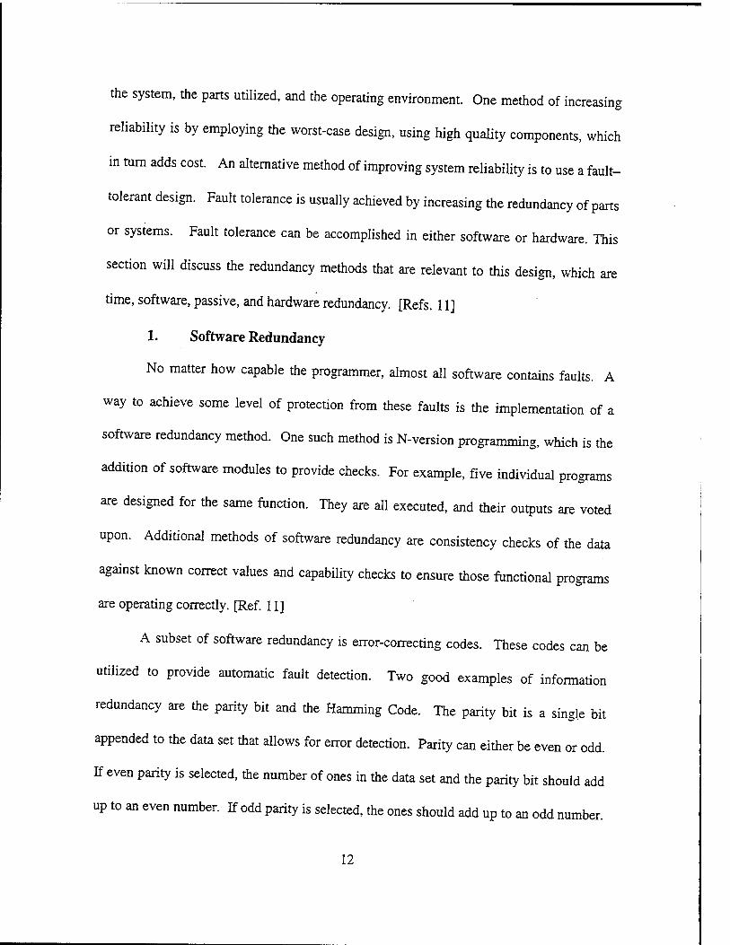
a) Triple Modular Redundancy (TMR)
A subset of passive hardware redundancy is the Triple Modular Redundant
(TMR) system. As the name implies, the TMR system takes the outputs of three
replicated modules and compares them in a voting unit. The voting unit passes the most
common input to the output, essentially masking out any single fault. The heart of a TMR
system, the voting unit, and its truth table are shown below in Figure 2.1 and Table 2.1.
14
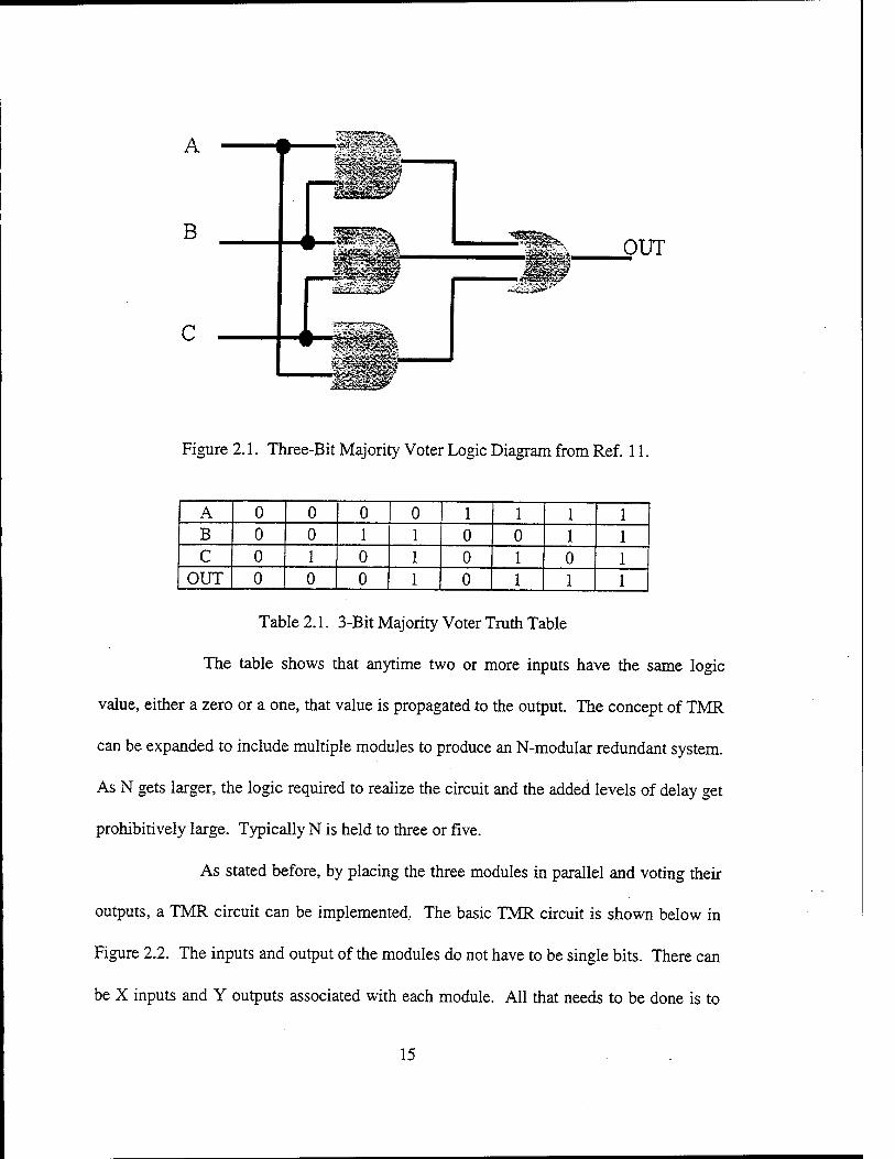
A
B
C
OUT
Figure 2.1. Three-Bit Majority Voter Logic Diagram from Ref. 11.
A 0 0 0 0 1 1 1 1 B 0 0 1 1 0 0 1 1 C 0 1 0 1 0 1 0 1
OUT 0 0 0 1 0 1 1 1
Table 2.1. 3-Bit Majority Voter Truth Table
The table shows that anytime two or more inputs have the same logic
value, either a zero or a one, that value is propagated to the output. The concept of TMR
can be expanded to include multiple modules to produce an N-modular redundant system.
As N gets larger, the logic required to realize the circuit and the added levels of delay get
prohibitively large. Typically N is held to three or five.
As stated before, by placing the three modules in parallel and voting their
outputs, a TMR circuit can be implemented, The basic TMR circuit is shown below in
Figure 2.2. The inputs and output of the modules do not have to be single bits. There can
be X inputs and Y outputs associated with each module. All that needs to be done is to
15

place Y single bit voters in parallel, connected such that they vote each of the respective
Y outputs.
Input A
Input B
Input C
•^"■.jJ--!Vyi:i->JL^i.-->a.V.WJ'*!>'lJ-.i
:"MöaB>'';v
,i.-Modj3p-. mammäm
Figure 2.2. Basic TMR Circuit Implementation from Ref. 11.
The single voter on the output of the TMR system is a single point of
failure. That is, if the voter fails and generates or propagates an error, then the error will
be propagated throughout the circuit. This could become a major problem in cascaded
circuits. To solve this problem, the voters at the end of each stage can also be tripled. An
example of this is shown in Figure 2.3. [Ref. 11]
Ihput A
Input B
Input C
Modi
Figure 2.3. Tripled TMR Voters from Ref. 11.
16

B. TMR MICROPROCESSOR DESIGN
The framework for the system implemented in this work was originally designed
and simulated by Lieutenant John C. Payne, Jr., USN, as a Fault Tolerant Computing
Testbed using the Verilog design suite. Following this, Captain David Summers, USMC
improved, implemented and fabricated the design and Lieutenant Damen Hofheinz, USN
continued implementation and testing of the testbed. The remainder of this section is a
brief synopsis of the TMR Testbed Design. For a more detailed explanation, please see
Ref. 1, Ref. 2 and Ref. 3.
1. Processor Selection
Lt. Payne began his design with the logical step of selecting a microprocessor. In
his selection process he took into account such factors as COTS vs. Radhard, CISC vs.
RISC, size, pinout, power, bus width, memory size, speed, and multiple chip vs. single
chip implementations. His research led him to select the MIPS R3081 RISController
produced by Integrated Device Technologies (IDT). This device was selected over
AMD's AM29000 and AM29050; IBM and Motorola's PowerPC 603e, 604e, and 750;
and IDT's R36100, R4650, and R5000. The determining factor for selecting the R3081
was the availability of radiation environment performance data because the processor had
to be latch-up resistant. The R3081 was tested in a space experiment by the Naval
Research Laboratory (NRL) to measure SEU and total dose effects on the processor.
Another factor was the compact size of the R3081 due to its small number of pins. A
detailed description of the R3081 can be found in Ref. 12.
17
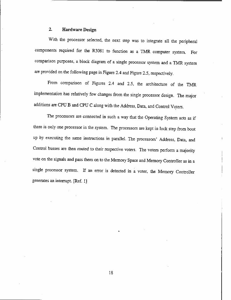
2. Hardware Design
With the processor selected, the next step was to integrate all the peripheral
components required for the R3081 to function as a TMR computer system. For
comparison purposes, a block diagram of a single processor system and a TMR system
are provided on the following page in Figure 2.4 and Figure 2.5, respectively.
From comparison of Figures 2.4 and 2.5, the architecture of the TMR
implementation has relatively few changes from the single processor design. The major
additions are CPU B and CPU C along with the Address, Data, and Control Voters.
The processors are connected in such a way that the Operating System acts as if
there is only one processor in the system. The processors are kept in lock step from boot
up by executing the same instructions in parallel. The processors' Address, Data, and
Control busses are then routed to their respective voters. The voters perform a majority
vote on the signals and pass them on to the Memory Space and Memory Controller as in a
single processor system. If an error is detected in a voter, the Memory Controller
generates an interrupt. [Ref. 1]
18

Figure 2.4. Simple R3081 Board Design from Ref. 2.
R3081 RISC
CPU A
R3081 RISC
CPUB
R3081 RISC
CPUC
Address Latches
Address Busses
Address Latches
Address Voter
Voted Address
Bus
Address Error
Address Latches
Data Susses
RAM
Data Voter/Xcvr
Data Error
Voted Data ' Bus
Control Busses
t—
Control Error L_ Control Voter
Voted Control
Bus
Memory/ Error
Controller
Vote Error Interrupt
EPROM
Figure 2.5. TMR R3081 Board Design from Ref. 1.
19
3. Fault Detection and Recovery
The voters allow the fault generated in one of the processors to be masked out and
the bus cycle to complete correctly, but that does not completely remedy the situation.
The processor that had the error is now out of synchronization with the other two
processors. That is where the Interrupt Handler comes into play.
When a voter detects a miss compare on its inputs, it signals the Memory
Controller, which asserts an interrupt input to the processors. The Interrupt Handler
resets the invalid processor in a very simplistic way. It starts by saving the processors'
internal registers to memory. Since all three processors will be executing the instructions
to save the internal registers, the Data Voter will mask out the invalid data from the
corrupted CPU. The Interrupt Handler then reloads the processors' internal registers from
memory. This puts the corrupted processor back into synchronization with the other two
processors. The Interrupt Handler then acknowledges the interrupt and returns from the
exception. The processors then continue execution with the next instruction.
In order to determine which processor was corrupted, the internal registers of each
processor must be examined. The data must be captured prior to being voted or the error
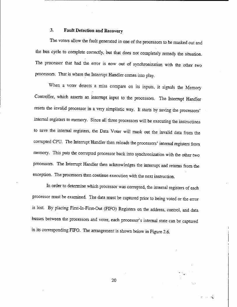
is lost. By placing First-In-First-Out (FIFO) Registers on the address, control, and data
busses between the processors and voter, each processor's internal state can be captured
in its corresponding FIFO. The arrangement is shown below in Figure 2.6.
20

R3081 RISC
CPU A
Address Latches
Address Bus.
Data Bus
Control Bus
Buffer A
7Y2
FIFO A
R3081 RISC
CPUB
Address Latches
Address Bus .
Data Bus
Control Bus
Buffer B
R3081 RISC
CPUC
Y
FIFO B FIFO Write
Enable & Buffer Select
Lines
From Memory
Controller
Figure 2.6. TMR FIFO Interface from Ref. 1.
C. DESIGN IMPLEMENTATION
Lieutenant Payne's design and simulations was the framework for the concept of
the TMR system. His design product was the software verification in Verflog of his
implementation of TMR. The thesis presented by Captain David Summers, [Ref. 2],
describes the implementation of the TMR design in hardware and the required changes.
Finally, the thesis presented by Lieutenant Hofheinz, [Ref. 3], completes the hardware
implementation and shows the results of the preliminary testing of the testbed. The
following paragraphs will provide a brief overview of these design changes and further
information regarding them can be found in Ref. 1, Ref. 2 and Ref. 3.
21
The process in the design of any system is driven by many factors including part
availability and compatibility. The three major changes Captain Summers was required to
implement in order to provide a working board for future test and space applications were
the addition of a system controller FPGA and I/O interface ports. The system controller
FPGA was added to replace some of the functionality provided by the computer in the
Verilog design of Ref. 1. The I/O interface was added to provide the means to upload
programs and control the board during testing.
The design and manufacture of the TMR board were completed by Captain
Summers, but he was unable to complete the programming of the System Controller
FPGA, and testing and verification of the overall design. Lieutenant Hofheinz continued
and completed this follow-on work as part of the preparation of the board for eventual
cyclotron testing and space-based applications. The follow-on work carried out by
Lieutenant Hofheinz included the design and implementation of the system controller
FPGA as well as doing the preliminary tests and verification of the system functions.
These design changes are highlighted and shown in Figure 2.5.
The joint efforts of Lieutenant Payne, Captain Summers and Lieutenant Hofheinz
proved the fundamental concept and produced a working example of a TMR system.
Beginning with the next chapter, the design of a new TMR system using 64-bit
microprocessors is presented.
22
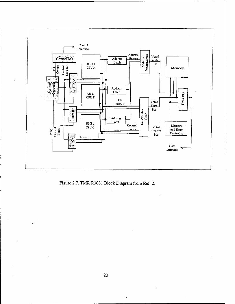
Control —w Interface
Address Rn«p<:
D Ol E u u
>
Control I/O
R3081 CPU A
Voted — AHHrecs
Memory
Latch Anrir
>1 I Bus
c CO
Q
I—
I O O:. - tS :-SV.:
<
»
:5"? j"
€ R3081 CPUB
A Aft
Latch O
a « a
Data T 1 Russe'; ( 1 I Voted
"3 B w
ü B ]3 > «
Dnrn (
O
►—
-g . E
l>
R3081 CPUC
. _< ► Address Latch 1
Control Rinne«
1 —H
Voted Control
Memory and Error Controller
o c £ u -1
5. u. HI
Bus
Data Interface
^ 1
Figure 2.7. TMR R3081 Block Diagram from Ref. 2.
23
THIS PAGE INTENTIONALLY LEFT BLANK
24

in. MICROPROCESSOR SELECTION
The intent of this thesis is to take another step in the design and implementation of
a fault tolerant TMR system by using 64-bit COTS microprocessors. The benefits of
using COTS parts and implementing the TMR concept using them have been mentioned
in the previous chapter. The benefit expected from this work is the performance
improvement of the TMR system by further exploitation of the power of COTS devices.
One of the features of a microprocessor that is expected to enhance performance is the
address/data bus width. The wider the bus width is, the more data is processed per bus
cycle. The growing number of applications using 64-bit microprocessors and the wide
range of 64-bit microprocessors available supports the rationale for this work. This thesis
was driven by that challenge of whether a more capable and current microprocessor could
be used in the TMR design and the necessary changes to the current design in order to
accommodate that kind of microprocessors.
This chapter presents the process of microprocessor selection. The system design
depends on the type of microprocessor to be used, so the first step is to select the
microprocessor. The challenge in selecting a microprocessor was the availability of a
wide range of 64-bit microprocessors. In order to reduce the number of candidates and
focus in on the best choice, certain criteria had to be brought up and employed. The
following sections explain the criteria used for the selection of the microprocessor to be
used, the variety of microprocessors available and their characteristics, and the
characteristics of the microprocessor that was selected and used in this design.
25

A. CHARACTERISTICS & CRITERIA
The first step in microprocessor selection is to set up the criteria on which the
selection process is to be based. The characteristics of different microprocessors are
reviewed and the decision is made on which microprocessor best suits the design at hand.
The criteria consisted of considerations such as COTS vs. rad-hard, CISC vs. RISC, size,
pin-out and power consumption, performance, bus width and compatibility to the
previous system.
1. COTS vs. RadHard
As discussed previously in Chapter I, the availability, cost and performance of
COTS devices compared to rad-hard devices present significant advantages in using
COTS devices. First of all, COTS devices tend to be state-of-the-art and therefore more
capable than rad-hard devices. Second, COTS devices are widely available and they offer
a wide variety to the designer. Third, rad-hard. devices often have uncertain delivery time,
which adds to the overall system design time. These devices often must be specially
ordered from a limited number of vendors due to declining rad-hard device market. On
the contrary, COTS devices, as the name implies, are available over the counter in a short
time. Fourth, the software support and compatibility for COTS devices is better than rad-
hard devices. Usually, the software must be specially designed for rad-hard devices and
thus, is less proven, more expensive and takes more time to develop. Finally, the cost of
rad-hard devices are multiple times higher than that of COTS devices which have
multiple times better performance compared to their rad-hard counterparts.
26

However, COTS devices have disadvantages, too. First of all, the techniques used
to design fault-tolerant systems utilizing COTS devices require the use of both part
redundancy and physical shielding which contribute to the overall system cost, weight
and space restriction on the board. Second, while some COTS devices may have hardness
levels of 100 kRads or more, this hardness varies greatly from device to device and is less
proven than rad-hard devices. Third, in many cases, the safety and reliability
specifications for military applications cannot be met by COTS devices. Lastly, as the
semiconductor industry changes technology and the devices get smaller, faster and more
complex, they are becoming more susceptible to radiation.
2. CISC vs. RISC
Reduced Instruction Set Computer (RISC) machines are designed to reduce the
number and complexity of instructions in the microprocessor, thus allowing a reduction
of actual hardware complexity. The simpler the hardware, the less susceptible it is to
radiation-induced failures. RISC machines take advantage of caching, prefetching,
pipelining and superscalar methods to improve performance while CISC machines are
unable to take full advantage of these due to their variable-length, complex instructions.
3. Size, Pinout, Power
The size of the device determines the physical space requirement. Since the
weight and space constraints are critical limitations in space applications, smaller devices
with smaller number of pins are preferred. Many devices have reduced number of pins by
having multiplexed address and data busses. Similarly, power consumption is another
27
critical factor to take into consideration when selecting a device to be used in space
applications where power is a precious commodity.
4. Bus Width
The bus width of COTS devices follows the current trends. Although many
systems still effectively employ 32-bit microprocessors, the current trend is towards 64-
bit busses to improve the performance of the machine by increasing the amount of data
processed in each cycle. While some manufacturers realize this transition by offering
microprocessors with flexible bus width that can be switched between 32 bits and 64 bits,
the others offer strictly 64-bit architectures.
Although the 64-bit architecture brings increased power consumption and
hardware complexity, the performance benefits of using a 64-bit microprocessor, which is
increasingly finding more commercial applications and growing its market share, weighs
heavier.
5. Speed
One of the most important factors in selecting a microprocessor is its speed which
is basically the clock rate the machine runs at and which has considerable effect in
determining overall system performance. However, the speed, thus the system
performance, will be limited by the additional propagation time introduced by the voting
and control logic in a TMR design. The processor chosen for this design may not have the
highest speed available in the market due to the performance penalty of TMR technique
but should still introduce a performance leap when compared to the R3081, TMR design
in Ref. 2 and Ref. 3.
28

B. REVIEW OF CURRENT MICROPROCESSORS
As part of this research, several microprocessors were analyzed based on the
criteria discussed in the previous section. The microprocessor to be selected would
obviously be a COTS device due to their numerous advantages explained earlier in detail.
So there was no need to include rad-hard devices in this process. Table 3.1 contains data
concerning the various microprocessors that were considered. These are all RISC
processors because the first criteria employed in selection process was the RISC vs. CISC
consideration and RISC processors were focused on due to their advantages mentioned
before.
Microprocessor Data Bus Address Bus Performance in
Dhrystone MIP S
Number of Pins Power (W)
IDT79R3081 32 32 40 @ 50 MHz 84 2.375-4.125
EDT79RC32364 32 32 175 @ 133 MHz 144 0.6-0.9
IDT79R4700 64 64 260 @ 200 MHz 179/208 4.25-7.5
IDT79RC5000 64 64 330 @ 250 MHz 223/272 7.59-8.25
IDT79RC4650 32/64 32/64 175 @ 133 MHz 208 1.646-3.465
IBM PowerPC 40IGF 32 32 53 @ 50 MHz 80 0.2
IBM PowerPC 403GCX 32 32 112 @ 80 MHz 160 0.51
IBM PowerPC 405CR 32 32 282 @ 200 MHz 316 0.8
IBM PowerPC 603e 32/64 32/64 135 @ 100 MHz 240/255 3.5-5.8
IBM PowerPC 750CX 32/64 32 1160@500MHz 256 4.7-11.0
Motorola PowerPC
MPC/MPEC603e
32 32 188 @ 133 MHz 240/255 3.5-5.8
Table 3.1. List of Candidate Microprocessors.
29

C. CHARACTERISTICS OF SELECTED MICROPROCESSOR
The microprocessor chosen was IDT79RC4650 RISC Processor manufactured by
Integrated Device Technologies (IDT). The RC4650 is a single-chip, COTS RISC
architecture with a 32/64-bit multiplexed address/data bus. The determining factor in
selecting the RC4650 was its numerous similarities and its compatibility with the R3081
processor that was used in the previous design, as well as its higher performance, its 64-
bit multiplexed address/data bus width, which is one of the driving factors of this thesis,
and its compact size. One concern is that not all COTS devices are suitable to be used in
TMR system. They need to be resistant to destructive radiation effects such as total dose
effect, SEL or SEB. However, the radiation environment performance data for the
RC4650 was not available at the time of research. Thus, its selection is conditional,
subject to the risk of experiencing a destructive fault due to total dose effect, SEL or SEB.
However, this is a concept design and a future design based on a processor resistant to
destructive effects can use basically the same concept.
The IDT79RC4650 is a low-cost, simplified and power sensitive microprocessor
that offers high performance through 64-bit architecture, high-speed pipelines and high-
bandwidth caches and bus interface. [Ref. 13] The main features of the RC4650 include:
• 64-bit architecture with 64-bit integer operations, 64-bit registers and 64-bit multiplexed address/data busses.
• High performance microprocessor with DSP capability at 175 Dhrystone MIPS, 66.7M Multiply-Add per second or 44 Mflops at 133 MHz
• High level of integration provides 64-bit integer CPU, single-precision floating- point unit and integer DSP/multiply unit
30

• Large, on-chip, user configurable, 2-way set associative 8KB data and 8KB instruction caches
• Bus compatible with RC4600 and RC4700 family of processors
• Low power operation at less than 2W at 100 MHz and active power management units
• Low-cost 208-pin package
Figure 3.1 shows a block diagram of the IDT79RC4650 microprocessor. Some of
the highlights are:
• System Control Coprocessor (CPO) • translates virtual addresses into physical addresses • manages exceptions and transitions between kernel and user states • controls cache subsystem • controls the power management unit.
• Floating Point Coprocessor (CP1) • Decodes and executes instructions in parallel with the integer unit • Performs single-precision arithmetic • Operation set includes floating-point add, subtract, multiply, divide, square
root, conversion between fixed-point and floating-point format and compare.
• Integer CPU core • 32 general purpose 64-bit registers • ALU, shifter, multiply/DSP unit, pipeline controller
• User configurable instruction and data caches
• 32/64 bit synchronized system interface
31

133 MIPS 64-bit Orion CPU System Control Coprocessor
Register fill
a e a £ .» a.
Adder
Load iligrter
Store Aligner
Logic Unit
Higb-Perforoanct Integer Muliphr/DSP
Address Translation/ Cache Attribute Control
Exception Management
Functions
l n £
Control Bus
InslructionBus
Instruction Cache Set A
lUciable)
Instruction Cache SetB
R PitiBll?
Synchronized System Interface
«MFLOPS Single-Precision FPA
u x a.
FT
FP regster fie
Pact/Unpack
FP Add/SuUCrU
DMSqrt
FP Mulipry
3 I
Data Cache Set A
(Loekable|
Dab Cache SelB
Figure 3.1. RC4650 Block Diagram from Ref. 13.
1. System Control Coprocessor (CPO)
The integrated on-chip System Control Coprocessor manages virtual to physical
address translation and the exceptions and transitions between user and kernel states. By
sharing common virtual addresses that are mapped to separate physical addresses, the
RC4650 supports multiple user tasks in parallel. This facility enables multiple user
processes in a single physical memory without the use of a TLB and is implemented via
the base-bounds registers in CPO. Kernel mode addresses do not use the base-bounds
registers but rather undergo a fixed virtual to physical address translation. CPO also
32

controls the cache subsystem as well as providing diagnostic control and error recovery
facilities. In addition, it is used to control the power management unit in order to reduce
power consumption of the internal core of the CPU. [Ref. 13]
2. Floating Point Coprocessor (CP1)
The RC4650 incorporates an on-chip, single-precision floating-point coprocessor
that includes a floating-point register file of 32 32-bit registers and execution units. The
floating-point coprocessor forms a seamless interface with the integer unit, decoding and
executing instructions in parallel. CP1 performs single-precision arithmetic as specified
in IEEE Standard 754. The execution unit is broken into a separate multiply unit and a
combined add/convert/divide/square root unit. The floating-point unit's operation set
includes floating-point add, subtract, multiply, divide, square root, conversion between
fixed-point and floating-point format and floating-point compare. [Ref. 13]
3. CPU Core
The CPU core is a pipelined, 64-bit RISC integer execution unit that includes
ALU, shifter, multiply/DSP unit and pipeline controller. It features a load/store
architecture with single-cycle ALU operations and an autonomous multiply/divide unit.
The register file has 32 64-bit registers, two read ports and one write port. The RC4650
uses a 5-stage pipeline that requires fewer stalls. Once the pipeline is filled, five
instructions are executed simultaneously. The simplicity of the pipeline allows the
RC4650 to be lower cost and less power-consuming than super-scalar processors. [Ref.
13]
33
4. Instruction and Data Caches
The RC4650 incorporates 2-way set-associative, virtually-indexed, physically-
tagged, on-chip data and instruction caches default configured to 8kB each. Both the
instruction cache and the data cache are organized with line sizes of 32 bytes (8
instructions in the instruction cache) to maximize performance. The default write policy
in the data cache is write-back, which means that a store to a cache line doesn't
immediately cause memory to be updated. This increases system performance by
reducing bus traffic and eliminating the bottleneck of waiting for each store operation to
finish before issuing a subsequent memory operation. However, the data cache can be
reconfigured to write-through mode. Associated with the data cache is a store buffer that
allows the RC4650 to execute a store instruction every processor cycle without penalty.
In addition, there is a 4-deep on-chip write buffer, that holds up to 4 data and address
pairs and decouples the speed of the processor from the speed of the memory system,
minimizing processor stalls due to data write operations. [Ref. 13]
The influence of internal caches on TMR system has. not been addressed in this
thesis. The TMR concept of error recovery does not include dealing with errors in internal
caches. Instead, the internal caches are invalidated by the interrupt handling routine
during the context switch operation, which restores the processor register contents to an
error-free state.
5. System Interface
The system interface of the RC4650 consists of a 64-bit multiplexed address and
data bus called SysAD, a 9-bit command bus called SysCmd and 6 handshake signals,
34
namely RdRdy*, WrRdy*, ExtRqst*, Release*, Validln*, ValidOut*. Cycles in which
SysAD bus contains a valid address are called address cycles and cycles in which SysAD
bus contains valid data are called data cycles. Validity of the contents of SysAD and
SysCmd busses is indicated by the Validln* and ValidOut* signals. The command bus
specifies the nature of the request, whether a read cycle or a write cycle will take place,
and identifies the contents of SysAD bus, either address or data, during any cycle in
which it is valid. The RdRdy* and WrRdy* signals determine whether a read or a write
cycle is beginning. After one of them is sampled, the processor initiates corresponding
cycle by putting a valid address on the SysAD bus. The Extrqst* and Release* signals are
used to control the transition between master and slave states if there are more than one
possible bus masters in a system. [Ref. 13]
A bus interface of a typical RC4650 system contains transparent latches to
demultiplex address and data busses. The data path between the memory system and the
processor is managed by octal transceivers and a set of PLDs or an FPGA that is used to
control the handshake process between the memory system and the processor. A typical
RC4650 system is presented in Figure 3.2. [Ref. 13]
This chapter has discussed the issues relevant to the microprocessor selection
process and presented a review of the RC4650 microprocessor features. Having selected
the microprocessor, the hardware design of the new TMR system using the RC4650
microprocessor will be presented in the following chapter.
35

RC4650
" 4 Address Boot ROM
DRAM (80ns)
32 or 64 il_
TZ ^
T 32 Of 64
y
4 Control
SCSI
4- Control
- / Control
Memory I/O Controller
^JL
ENET
r Figure 3.2. Typical RC4650 System Architecture from Ref. 13.
36

IV. HARDWARE DESIGN
The scope of the design described in this thesis does not include the full
functionality of the design in Ref. 2 and Ref.3, such as loading and running of user
programs. This design rather focuses on the possibility of implementing a TMR system
using 64-bit microprocessors and determining a reasonable performance level achievable
in the new design, such as maximum clock rate this processor can run at in a TMR
design.
Having selected the 64-bit microprocessor, the next step was to identify and
implement the changes necessary to accommodate this processor in a TMR design. In
some areas, the RC4650 has such compatibility with the R3081 that little or no changes
were necessary from the design in Ref. 2 and Ref.3. Examples include memory space and
memory decoding unit. This was not the case for other parts of the design where
significant changes were necessary, such as the system interface and handshake signals.
A. MICROPROCESSOR AND LATCHES
The key element in the system is the microprocessor. In the case of TMR system,
there are actually three microprocessors. Since the address latches are used to demultiplex
the address/data busses, they are presented here with the microprocessors. In addition, the
SysCmd bits issued by the processors at the beginning of each read/write cycle are latched
to make them available for the rest of the read/write cycle and that latch is presented here,
too. The schematic diagram of the three microprocessor and the associated latches are
given in Figure A.2 in Appendix A.
37
1. Microprocessor
The microprocessor used in the design in Ref. 2 and Ref.3, the R3081, ran at
clock rates of up to 40 MHz with a half-frequency bus. On the other hand, the RC4650
has operation frequencies from 100 MHz up to 267 MHz. This allows a great
improvement in performance compared to previous design, thus addressing one of the
main advantages of using COTS devices. However, there are some factors that need to be
taken into account when selecting the operational clock rate. Although the processors can
execute instructions internally at very high speeds, the actual performance is limited by
the bus speed. The speed of external busses that connect processors to peripheral units
cannot keep up with the internal speeds of modern microprocessors. So, whenever the
processor needs to access external resources, the execution of the instruction is limited by
the bus speed. Similarly, the semiconductor industry has not improved the speeds of
memory chips as much as they improved the speeds of microprocessors. In addition to
these, the propagation delay due to the voting logic is the most important factor limiting
the execution speed in a TMR system. The voting circuitry inserted between the
microprocessor and the memory system adds two more levels of logic, which increases
the propagation time of voted signals (address, data and control) between the
microprocessor and the memory system. Other signals generated by the programmable
devices based on some of the voted signals are also delayed due to voting. Thus, the clock
rate the processors will run at was decided after the voting logic was designed and the
timing analysis of the system was completed. A slow clock rate would degrade the overall
system performance while a high clock rate would introduce excessive number of wait
38
states and stall the pipelined processors during a memory access. The simulation results
presented in Chapter VI showed that a clock rate of 100 MHz would be ideal for the
design without excessive number of wait states in each memory access cycle.
2. Latches
In order to reduce the pin count of the RC4650, IDT chose to multiplex the
address and data busses into a SysAD bus. This generates a requirement for the designer
to split the SysAD bus into data and address busses by using latches. Similarly, the bi-
directional SysCmd bus needs to be latched because the command identifier issued during
the address cycle on the SysCmd bus contains control bits that are used to generate the
memory interface signals. These signals are shown in the programmable device design
equations in Appendix B. Normally, demultiplexing is done by using transparent latches
that allow the address to appear on the address bus a short propagation delay after the
latches are enabled. Since the processor has no pin that indicates the signal on the
multiplexed address/data bus is data or address, the latch enable signal has to be
generated externally by the designer. The latch enable signal was generated by a NOR
gate whose inputs are the most significant bit of SysCmd bus (SysCmd[8]) and
ValidOut* signal. ValidOut* is an active-low signal that indicates the signal output on
SysCmd and SysAD busses by the processor are valid. SysCmd[8], when low, indicates
that the current clock cycle is an address cycle, thus the signals on SsyAD bus is an
address and the signals on SysCmd bus is a command identifier. The same signal enables
both the address latches and the SysCmd latch because the processor drives both address
and SysCmd busses simultaneously.
39

B. MEMORY SPACE
There are three types of devices in the memory system of the TMR design:
Programmable Read Only Memory (PROM), Random Access Memory (RAM) and
memory-mapped I/O peripherals. This section will present an overview of the memory
space supported by the RC4650 and incorporation of PROM, RAM and I/O peripherals
into that memory space.
As mentioned in the section about the microprocessor selection, the memory
space supported by the RC4650 is the same as that of the R3081, which minimizes the
changes necessary in the memory decoder unit of the design in Ref. 2 and Ref. 3. As in
the case of the R3081, the RC4650 supports a 4 GByte memory space, broken down into
four distinct virtual address areas: kernel-user segment (KUSEG), kernel segment 0
(KSEGO), kernel segment 1 (KSEG1) and kernel segment 2 (KSEG2). KUSEG is a
cacheable 2 GByte area used for kernel and user processes. KSEGO is a cacheable 512
MByte space normally used for kernel executable code and kernel data. KSEG1 is a non-
cacheable 512 MByte area normally used for memory-mapped I/O, boot ROM code and
operating system data. KSEG2 is a cacheable 1 GByte area normally used by operating
system for stacks, process data and dynamically allocated memory. A diagram of the
virtual memory segments is shown in Figure 4.1 and the corresponding virtual address
ranges are given in Table 4.1. [Ref. 13]
Although the RC4650 supports a 4 GByte memory space, the entire space is not
usually populated. The size and location of the memory space populated in this design is
explained in following sections.
40

Ox FFFF FFFF
OrCOOO OOOff
tttADOO OOOO
uiaocoiiooo
Unmapped
0.5 GB Unmapped Uncadietf
0.5 GB Unmapped Cached1
Ox CC03 COO»
2 GB
Mapped
tsegl
tscgl
tsegO
tuseg
Figure 4.1. Virtual Memory Segments supported by RC4650 from Ref. 13.
Address Bit
Values
Status Register Is
One Of These Values
Segment Name
Virtual Address Range
Segment Size UNI EXL ERL
A(31) = 0
UM-0
or
EXL = 1
or
PDI „1
kuseg 0x0000 0000 through 0x7FFF FFFF
2 Gbytes (2J1 bytes)
A(31:29) =
1002
ksegO 0x8000 0000 through 0x9FFF FFFF
512 Mbytes {229
bytes)
A(31:29) =
1012
ksegl OxAOOO 0000 through OxBFFF FFFF
512 Mbytes (229
bytes)
A(31:30) = 112 kseg2 OxCOOO 0000 through OxFFFF FFFF
1 Gbyte (232 bytes)
Table 4.1. Address Range of Memory Segments supported by RC4650 from Ref. 13
41
1. PROM
As explained in Ref. 2, the size and type of PROM is dictated mainly by the
operating system. Since this design merely focuses on the incorporation of a 64-bit
microprocessor into the previous 32-bit system and the selected processor is both
software and memory space compatible with the processor of the design in Ref. 2 and
Ref. 3, it was assumed that the same operating system PROM address space could be
implemented in this design. So, the location of the 512 KBytes of PROM within the 4
GByte memory space is the physical address space between 1FC0_0000 and 1FC7_FEFF.
One of the two changes in the design was the type of PROM chips being used.
Due to increased clock rate of the system, a faster PROM chip would be better in order to
avoid excessive number of wait states during accesses to PROM. Another version of the
PROM chip that was used in the design in Ref. 2 and Ref. 3, AMD 27C010-45 which has
a data access time of 45 ns and which is available from the same manufacturer (AMD),
was selected. The other change necessary was the use of eight of those chips instead of
four since data bus width is 64 bits in the current design while it was 32 bits in the design
in Ref. 2 and Ref. 3. The schematic of the PROM memory unit can be found in Figure
A.5 in Appendix A.
2. SRAM
The size and location of SRAM memory space is also based on the design in Ref.
2 and Ref. 3 due to the same reasons expressed in the PROM section, namely software
and memory space compatibility of the microprocessors used in the two systems. The
factors leading to the selection of SRAM memory size and location was discussed in Ref.
42
2. In the case of SRAM memory space, the only change necessary was the use of eight
instead of four SRAM chips in each of the five 0.5-MByte SRAM blocks due to the
expansion of data bus width from 32 bits to 64 bits, bringing the total number of chips to
40 compared to 20 in the design in Ref. 2 and Ref. 3. The same types of SRAM chips
(IDT71024S12) were used because the access time of 12 ns was sufficient for the new
system with the increased clock rate.
As discussed in the beginning of the memory section, the RC4650 supports four
distinct virtual address segments. From Ref. 2, the design was determined to consist of
five 0.5-Mbyte SRAM blocks. These are denoted as KRAM, URAMO, URAM1, URAM2
and URAM3 in the schematic diagram of SRAM memory unit, which can be found in
Appendix A. It was also determined that only two of the four virtual address segments
would be populated with SRAM which are KUSEG and KSEGO. One of the two SRAM
blocks allocated to the operating system (KRAM) was placed in memory segment
KSEGO to provide a random access memory location for the PROM contents to be
transferred to and executed from. The remaining operating system SRAM block and the
three user SRAM blocks (URAM0-URAM3) were placed in memory segment KUSEG.
The schematic diagram of the SRAM memory unit can be found in Figures A.6-A.8 in
Appendix A.
43

THIS PAGE INTENTIONALLY LEFT BLANK
44
V. PROGRAMMABLE LOGIC DESIGN
Several key functions in the TMR design are performed by programmable logic,
including programmable logic devices (PLD) and field programmable gate arrays
(FPGA). Most of the design changes required to accommodate a 64-bit microprocessor in
TMR system were made in this part of the system. The first step in the transformation
from the previous 32-bit design to the current 64-bit design was to understand the
functions performed by the programmable logic in the design in Ref. 2 and Ref. 3 and
reconfigure the programmable devices to perform the same functions in the new design.
Although the RC4650 was selected due to its similarities and compatibility with the
R3081 of the design in Ref. 2 and Ref. 3, it had a completely different system interface
which required considerable change in the design of programmable logic devices that
generate the memory interface signals.
The functions performed by the PLDs and the FPGAs were clearly defined and
distinct in the design in Ref. 2 and Ref. 3, which facilitated understanding how the system
worked. The two PLDs were designed to perform memory control and memory enable
functions while the FPGAs were designed to perform voting, address decoding and
system controller functions. The first approach was to follow the same technique by
dividing the functions among each device in the same way. The initial design showed that
the differences in the system interfaces of the two microprocessors, especially the
complexity of the RC4650 system interface compared to that of R3081, required the use
of twice as many PLDs as was used in the design in Ref. 2 and Ref. 3 if the functions
performed by PLDs and FPGAs were to be divided in the same distinctive way. However,
45

the restrictions imposed by the space and power limitations of a space application dictated
the use of as few devices as possible to perform the same functions.
The second approach was to include the functions performed by PLDs into an
FPGA to reduce the number of devices being used, thus covering less space and
consuming less power. But this approach was not feasible due to the longer propagation
delay of the FPGAs being used compared to that of the PLDs. Some memory control
signals had to be generated in a shorter time than could be achieved by the FPGA,
otherwise the read/write cycle would be stalled with a prohibitively excessive number of
wait states. The propagation delay of the FPGA would allow the system to achieve only
twice the performance level of the R3081 TMR system, which means a system clock rate
of 20 MHz vice 10 MHz clock rate of the R3081 TMR design. This was not a satisfactory
performance improvement compared to what was expected from this system designed
using a 64-bit modern microprocessor capable of running at clock rates of up to 267
MHz.
The final design of the programmable logic incorporated two functions. First one
is generating some critical memory control/enable signals, which might have an adverse
effect on system interface timing, by using PLDs. This allows minimizing the number of
PLDs to be used. Second one is generating other memory control/enable signals, which
did not cause additional wait states, by using FPGAs. This approach led to a design using
two PLDs and two FPGAs, which is considered to be the optimum design that
accommodates the 64-bit microprocessors.
46
A. FPGA DESIGN
The system in Ref. 2 used three FPGAs to perform voter, address decoder, timer
and system control functions. Since the scope of this thesis includes the feasibility
analysis of implementing the TMR fault tolerance concept using 64-bit microprocessors
and a performance evaluation rather than a complete TMR system design using 64-bit
microprocessors, this design focused on the core function in the TMR concept of voting
and error detection. For this reason, the system controller functionality was not
implemented in the FPGA design. The FPGAs in this design were used to perform the
functions of voting, address decoding and some of the memory control/enable functions
due to the design considerations explained in the previous section. This section presents
the FPGA selection process and the design of the two FPGAs used in the system.
Schematics of the FPGA designs are presented in Appendix C.
1. FPGA Selection
The initial approach in FPGA selection was using the same XILINX
XC4013XLA-PQ240 FPGAs from the design in Ref. 2 and Ref. 3 due to their advantages
explained in Ref. 2 and to facilitate continuity. The first consideration in the selection
process was the number of pins required for the function of each FPGA. Since RC4650
microprocessor issued 32-bit addresses although it has a 64-bit multiplexed address/data
bus, the address voting/decoding and the added functionality of voting the 9-bit system
command bus and generating some memory control/enable signals could be
accommodated in a XC4013XLA-PQ240 FPGA which offered 192 I/O pins. However,
voting the 64-bit data busses from the three processors to produce a 64-bit voted data bus
47
output requires at least 256 I/O pins, more than the total number of I/O pins available on a
XC4013XLA-PQ240 FPGA.
The second consideration was the requirement of the TMR concept to use
radiation hardened FPGAs since the FPGAs are a single point of failure in the TMR
concept. There were three members of the XC4000XLA family that had a radiation-
hardened version available at the time of the design. Only one of those three, the
XC4062XLA-BG432 package with 352 I/O pins, had enough number of I/O pins to
accommodate the data voting function, and that chip was selected to be used as the data
voter FPGA. [Ref. 14]
2. Address/Control Voter, Memory Decoder FPGA
The functions implemented in this FPGA are the majority voting of the three 30-
bit address and 9-bit system command busses, the decoding of the upper thirteen bits of
the voted address lines to generate chip select signals, and the generation of some of the
memory control/memory enable signals. The logic design of these functions is presented
in this section.
a) Address/Control Voter
Since the RC4650 multiplexes its address and data pins, latches are used
to separate the address and data busses. In this design, the system address/data busses,
SysAD, of the microprocessors are split into two different paths, one registered and the
other not. The registered path is the address path and the unregistered path is the data
path. When the RC4650 initiates a bus cycle, the SysAD bus is driven with the address to
be accessed and the ValidOut* signal is asserted which was used to generate the latch
48

enable signal. Then, the transparent latches drive the address bus with the latched address
to be accessed. The address is held on the address bus by the latch until the following bus
cycle when latches are enabled to latch a new address. The three address busses driven
similarly must be majority voted before being passed to the memory system.
The voting is done using macros, which are building blocks used to create
a hierarchical design in Xilinx Foundation Series Design Suite. Voting the address is
achieved by using the Majority Voter/Error Detector macros called VOTER4. Each
VOTER4 macro consists of four of the voter/error detector sub-macro presented in Figure
5.1 and votes three 4-bit inputs and generates a 4-bit majority-voted output and a 4-bit
error output that shows which bit in the 4-bit inputs had a mismatch. Since the number of
address lines voted is 30, eight of the VOTER4 macros were used for address voting.
Similarly, voting the 9-bit command identifiers from the three
microprocessors is achieved by using the Majority Voter/Error Detector macro called
VOTER9. The VOTER9 macro consists of nine of the voter/error detector sub-macros
presented in Figure 5.1 and one VOTER9 macro is sufficient for control voting. For more
information about the design and function of the sub-macro in Figure 5.1, see Ref. 2.
49
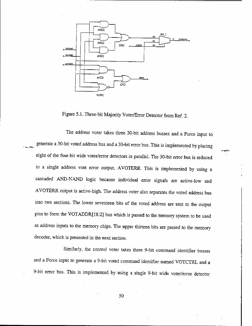
, DATA83
, DATAC3
AND2
f AN02 I
M2 1
0R3 rpRCg
AND2
0 VOTDATA
AND3 T> OR2
NOR3
Figure 5.1. Three-bit Majority Voter/Error Detector from Ref. 2.
The address voter takes three 30-bit address busses and a Force input to
^ generate a 30-bit voted address bus and a 30-bit error bus. This is implemented by placing
eight of the four-bit wide voter/error detectors in parallel. The 30-bit error bus is reduced
to a single address vote error output, AVOTERR. This is implemented by using a
cascaded AND-NAND logic because individual error signals are active-low and
AVOTERR output is active-high. The address voter also separates the voted address bus
into two sections. The lower seventeen bits of the voted address are sent to the output
pins to form the VOTADDR[18:2] bus which is passed to the memory system to be used
as address inputs to the memory chips. The upper thirteen bits are passed to the memory
decoder, which is presented in the next section.
Similarly, the control voter takes three 9-bit command identifier busses
and a Force input to generate a 9-bit voted command identifier named VOTCTRL and a
9-bit error bus. This is implemented by using a single 9-bit wide voter/error detector
50

module (VOTER9), which was mentioned above. The 9-bit error bus is reduced to a
single control vote error output, CVOTERR. This was implemented in the same way as
address vote error signal (AVOTERR) was generated as explained above.
Although not a part of the command identifier word, the ValidOut* signal
from the microprocessor is another control signal in the system interface that indicates the
validity of the signals on the address/data bus SysAD and system command bus SysCmd.
The ValidOut* signals from the three microprocessors are voted in the Address/Control
Voter FPGA and a voted ValidOut* signal, VotValidOut*, is output which is used to
generate some of the memory control/enable signals.
b) Memory Decoder
Memory decoder takes the upper thirteen bits of the voted address bus and
decodes them into chip select signals. A chip select signal is generated for each of the five
SRAM memory blocks, the EPROM, the UART, the Timer and the Interrupt
Acknowledge. Table 5.1 shows the chip select name, its physical address, its virtual
address and the memory segment it belongs to. The addresses correspond to the upper
thirteen bits of the voted address bus with zeros concatenated to the end. The table shows
that the Kernel SRAM resides in KSEGO, the remainder of the SRAM resides in the
KUSEG, and all of the peripherals and the EPROM reside in the non-cached KSEG1 as
discussed in Chapter IV. The Memory Decoder schematic is presented in Figure C.l in
Appendix C.
51

Signal Name Peripheral Physical Address
Virtual Address Memory Segment
KRAMCS* SRAM 0x0000 0x8000 KSEGO URAMOCS* SRAM 0x4000 0x0000 KUSEG URAM1CS* SRAM 0x4008 0x0008 KUSEG URAM2CS* SRAM 0x4010 0x0010 KUSEG URAM3CS* SRAM 0x4018 0x0018 KUSEG TIMERCS* TIMER 0x0440 0xA440 KSEG1
INTCS* INTERRUPT 0x1000 OxBOOO KSEG1 EPROMCS* EPROM Oxl FCO OxBFCO KSEG1 UARTCS* UART OxlFEO OxBFEO KSEG1
Table 5.1. Chip Select Memory Map from Ref 2.
c) Memory Control/Memory Enable Signals
Due to the reasons and design considerations mentioned at the beginning
of this section, read enable (RDEN*), read (RD), write (WR) and write data enable
(WRDATAEN) signals were generated using the Address/Control Voter FPGA where all
the signals required to generate these signals were available. The equations that represent
the design of the logic to generate those signals are presented in Appendix B.
The RDEN* signal works in concert with the chip select signals to activate
the output drivers of memory devices. Since all the logic between the processors and the
chip select signals is combinatorial, there is the possibility that the wrong chip select
signal may glitch while the voted address bus is settling, which may cause a wrong
memory address to be accessed. This is avoided by activating the outputs of the memory
devices with the RDEN* signal which is asserted later in the cycle after the chip select
signals stabilize and thus, gives memory device time to access the memory location and
move the data to its outputs. Unlike the write enable signals presented in the section on
52

PLD design, only one RDEN* signal is required since reads are done in complete words.
RDEN* signal is passed to all of the devices in the memory block in parallel.
The RDEN* signal is generated using the RESET*, CYCEND* signals
and the three bits from the voted command identifier that indicate the nature of the bus
cycle, VOTCTRL[7:5]. It is asserted when those three command identifier bits are 000
indicating a read request, unless RESET* or CYCEND* is asserted. It is de-asserted by
CYCEND* being asserted. This turns the output drivers of the memory device off at the
end of a bus cycle as soon as possible and reduces the possibility of bus contention.
RD signal was designed to decode the read request, represented in the
command identifier with the three bits VOTCTRL[7:5] being 000, into an active-high RD
signal in order to reduce the number of pins and thus, the complexity in the memory
enable/memory control logic.
Similarly, WR signal was designed to decode the write request,
represented in the command identifier with the three bits VOTCTRL[7:5] being 010, into
an active-high WR signal.
During a write cycle, the data from all three microprocessors are voted and
the voted data signals drive the voted-data-bus output of the Data Voter FPGA. Since not
all 64 voted data signals are generated at the same time due to different delays in each of
their individual paths, those signals will be bouncing for a short time before they settle.
To avoid those 64 data lines bouncing and generating noise, which may cause other
problems in the system, the voted data output of the Data Voter FPGA needs to be
enabled after a time when all signals in the voted data bus have settled. Hence,
53
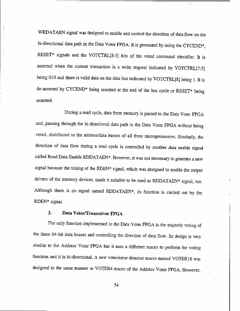
WRD ATAEN signal was designed to enable and control the direction of data flow on the
bi-directional data path in the Data Voter FPGA. It is generated by using the CYCEND*,
RESET* signals and the VOTCTRL[8:5] bits of the voted command identifier. It is
asserted when the current transaction is a write request indicated by VOTCTRL[7:5]
being 010 and there is valid data on the data bus indicated by VOTCTRL[8] being 1. It is
de-asserted by CYCEND* being asserted at the end of the bus cycle or RESET* being
asserted.
During a read cycle, data from memory is passed to the Data Voter FPGA
and, passing through the bi-directional data path in the Data Voter FPGA without bein*
voted, distributed to the address/data busses of all three microprocessors. Similarly, the
direction of data flow during a read cycle is controlled by another data enable signal
called Read Data Enable RDDATAEN*. However, it was not necessary to generate a new
signal because the timing of the RDEN* signal, which was designed to enable the output
drivers of the memory devices, made it suitable to be used as RDDATAEN* signal, too.
Although there is no signal named RDDATAEN*, its function is carried out by the
RDEN* signal.
3. Data Voter/Transceiver FPGA
The only function implemented in the Data Voter FPGA is the majority voting of
the three 64-bit data busses and controlling the direction of data flow. Its design is very
similar to the Address Voter FPGA but it uses a different macro to perform the voting
function and it is bi-directional. A new voter/error detector macro named VOTER16 was
designed in the same manner as VOTER4 macro of the Address Voter FPGA. However,
54

it consists of 16 of the sub-macro that was presented in Figure 5.1 instead of four. They
are connected in parallel and this gives a 16-bit wide voted output path. Thus, the number
of macros needed for a 64-bit data path is reduced to four. The four 16-bit error busses,
one from each macro, are combined in the same manner as the error busses in the Address
Voter to a single data vote error output named DVOTERR.
The Data Voter/Transceiver FPGA had to be designed for bi-directional data flow
because the information passing across the data bus flows in both directions: from
microprocessors to memory devices and from memory devices to microprocessors. The
data on the address/data busses of the three microprocessors need to be combined through
the voting logic and sent to the memory devices during write cycles. During read cycles,
the data on the single data bus coming from the memory devices needs to bypass the
voting logic and be split into three copies that drive the address/data busses of the three
microprocessors. This functionality was achieved using tri-state buffers enabled by the
RDDATAEN* and WRDATAEN signals to control the direction of data flow. The
design of this logic was done in Ref. 2 and the concept is presented in Figure 5.2 for one
of the 64 bits of the data bus. The transceiver design of Ref. 2 was expanded from a 32-
bit data path to a 64-bit data path to be used in this design.
55

■-•pa-T-ei ^
«■SATA««* Q-
Figure 5.2. One-bit Slice of the Transceiver Logic Design from Ref. 2.
During a write cycle, all three input pins are driven by the microprocessors. The
WRDATAEN signal enables BUFE tri-state buffers on each side of the voter logic. The
data flows through input tri-state buffers, the voter logic and the output tri-state buffers.
The voted data also returns towards input pins but it is blocked by the BUFT tri-state
buffers disabled by the RDDATAEN* signal.
During a read cycle, the input pin on the right side is driven by the memory
devices. The signal is routed through the input buffer and the three BUFT tri-state buffers
enabled by RDDATAEN* signal, to the output pins on the microprocessor side. The
WRDATAEN signal prevents data from flowing back into the voting logic by disabling
BUFE tri-state buffers.
56

B. PLD DESIGN
A different version of the ATF22V10C PLDs, which were also used in the design
in Ref. 2 and Ref. 3, was used in this design to facilitate continuity. It has a maximum
delay of 5 ns. The system design presented in Ref. 2 and Ref. 3 used two PLDs to perform
Memory Enable and Memory Controller functions. As stated in the previous section, in
this design, those functions are implemented in both PLDs and FPGAs due to the timing
requirements and the limited number of input/output pins available in the PLDs. In
addition, the memory enable and memory control functions are not divided among
different PLDs but performed mutually because one PLD would not be enough for the
memory enable function which requires 12 output pins while 22V10 PLD has only 10.
Thus, there is no distinction among the PLDs as memory control PLD and memory enable
PLD as was the case in previous design. Instead, they are called as PLD1 and PLD2.
The schematics showing how the PLDs are interconnected within the TMR
system are provided in Appendix A and the design equations used to program the PLDs
are provided in Appendix B. The next two subsections describe the functions of the
PLDs.
1. PLD1
When the microprocessors generate the signals initiating a bus transaction, the
address, data and control signals are voted, memory control signals are generated by the
FPGAs based on those voted signals and the necessary signals are passed on to the PLDs.
PLD1 uses lowest three bits of the voted command identifier (VOTCTRL[2:0]), read
signal (RD), write signal (WR), RESET*, system clock (SYSCLK), and the cycle end
57

Signal (CYCEND*) to generate the memory control signals Validln*, CYCEND* and the
memory enable signals WRENA*, WRENB*, WRENC*, WREND*. This section
describes the signals generated by PLD1.
a) Counter
Both PLD1 and PLD2 use an internal 4-bit counter to count the clock
cycles and to provide timing reference for different bus cycles. This allows the
microprocessor to interact with devices of various speeds by introducing wait states into
the bus cycle for devices that cannot respond in a single access time.
The counter is implemented in each PLD by using four of the ten I/O pins.
It uses the RESET*, CYCEND*, SYSCLK, RD and WR inputs to determine when to
count and when to reset back to zero. RESET* signal is used to reset the counter
whenever a system reset is required. CYCEND* signal is used to identify the end of the
current bus cycle and reset the counter back to zero. RD and WR signals are generated by
the Address/Control Voter FPGA using voted command identifier signals. Unless
RESET* or CYCEND* is asserted, the counter increments on each rising edge of
SYSCLK after RD or WR signal has been asserted.
b) Cycle End (CYCEND*)
The CYCEND* signal is an active-low signal used to indicate the end of
the current bus cycle. It is generated from RESET*, RD, WR, EPROMCS* inputs and the
counter contents. The timing of the CYCEND* signal is dependent on the latency
required to access the device and the type of bus cycle that is being run. RD and WR
signals are used to determine the type of bus cycle. The active-low EPROMCS* signal
58

and the counter contents are used to determine device latency. All the memory system,
except EPROM for which only read cycle is applicable, can perform a read in 7 clock
cycles or a write in 6 clock cycles. EPROM requires three additional wait states and
completes a read in 10 clock cycles.
c) Validln*
The Validln* is an active-low signal generated by memory control unit and
indicates to the microprocessors that memory is accessed and data placed on the
address/data bus is valid. The Validln* signal is generated using EPROMCS*, RD,
RESET* signals and the counter contents. Since address/data bus is driven by memory
only during a read cycle, this signal is only asserted on read transactions. All the memory
system, except EPROM, can perform a read in 7 clock cycles and Validln* is asserted at
the end of the read transaction when counter content is 7. Since access to EPROM
requires three additional clock cycles, Validln* is asserted when counter content is 10
during EPROM read cycle. Since the counter content changes every clock cycle, this
signal is asserted only for one clock cycle and then de-asserted.
d) Write Enable Signals
Since RC4650 supports byte, two-byte, three-byte, halfword, four-byte,
five-byte, six-byte, seven-byte and fullword writes, Write Enable strobes are used to
determine which bytes of the word are going to be involved in the transaction. The eight
write enable signals are WRENA*, WRENB*, WRENC*, WREND*, WRENE*,
WRENF*, WRENG* and WRENH*. WRENH* corresponds to the most significant byte
and WRENA* corresponds to the least significant byte. Since one PLD was not able to
59 "" '
generate all the eight write enable strobes as well as a 4-bit counter, the task was divided
between the two PLDs. However, it is more suitable to present all of the strobes in this
section because both PLD1 and PLD2 use the same inputs to generate these signals.
Write Enable strobes are generated using the least significant three bits of
the voted command identifier VOTCTRL[2:0], WR, RESET* signals and the counter
contents. RESET* signal de-asserts write enable strobes when system is reset. When WR
signal is asserted, the corresponding write enable strobes will be asserted based on the
coding in the least significant three bits of the command identifier. The truth table for this
function is given in Table 5.2. For the negative logic signals indicated by an asterisk, 0
signifies an asserted signal.
WR VOTCTRL[2:0] WRH* WRG* WRF* WRE* WRD* WRC* WRB* WRA*
000 1 1 1 1 0
001 1 1 1 0 0
010 1 1 0 0 0
011 1 0 0 0 0
100 0 0 0 0 0
101 0 0 0 0 0 0
110 0 0 0 0 0 0 0
111 0 0 0 0 0 0 0 0
Table 5.2. Byte Write Enable Strobes Assertion Table.
60
2. PLD2
When the microprocessors generate the signals initiating a bus transaction, the
address, data and control signals are voted, memory control signals are generated by the
FPGAs based on those voted signals and the necessary signals are passed on to the PLDs.
PLD2 uses lowest three bits of the voted command identifier VOTCTRL[2:0], read signal
(RD), write signal (WR), RESET*, system clock (SYSCLK), voted ValidOut* signal
(VotValidOut*), and the cycle end signal (CYCEND*) to generate the system interface
signals WrRdy*, RdRdy* and the memory enable signals WRENE*, WRENF*,
WRENG*, WRENH*. This section describes the signals generated by PLD2 other than
the write enable strobes and the 4-bit internal counter, which were mentioned in the
section about PLD1.
a) Read Ready (RdRdy*)
RdRdy* is an active-low signal used to indicate to the microprocessor that
memory system is ready for a read transaction. After the microprocessor senses that
RdRdy* is asserted, it initiates the read cycle by driving the address/data bus with a valid
address and the system command bus with a valid command identifier that indicates the
nature of the transaction and by asserting the ValidOut* signal that indicates the signals
on those two busses are valid. PLD2 uses CYCEND*, voted ValidOut* and the current
RdRdy* signals to generate the RdRdy* signal. RdRdy* is de-asserted when voted
ValidOut* signal is asserted meaning that processor has initiated a bus transaction.
RdRdy* stays asserted as long as voted ValidOut* is de-asserted meaning that the
processor hasn't initiated a bus transaction.
61
b) Write Ready (WrRdy*)
WrRdy* is an active-low signal used to indicate to the processor that
memory system is ready for a write transaction. After the processor senses that WrRdy* is
asserted, it initiates the transaction by driving the address/data bus with a valid address
and the system command bus with a command identifier that indicates the nature of the
transaction and asserting the ValidOut* signal that indicates the signals on those two
busses are valid. PLD2 uses CYCEND*, voted ValidOut* and the current RdRdy*
signals to generate the WrRdy* signal. WrRdy* is de-asserted when voted ValidOut*
signal is asserted meaning that processor has initiated a bus transaction. WrRdy* stays
asserted as long as voted ValidOut* is de-asserted meaning that the processor hasn't
initiated a bus transaction.
This chapter has presented the design of the programmable devices used in
the implementation of the TMR system. Having completed the hardware design
associated with this thesis, the results of the simulation of the system and the detailed
system timing analysis are presented in the next chapter.
62

VI. SYSTEM TIMING ANALYSIS
After the hardware and the programmable devices were designed, system
simulation and timing analysis was conducted. The purpose of the timing analysis is to
determine if the system operates as expected and to ensure that no bus contention occurs.
The system is designed to operate with a clock rate of 100 MHz, which means a clock
cycle of 10 ns.
The timing analysis was conducted on the two basic types of bus transaction:
Read Cycles and Write Cycles. The following sections present the results of the timing
analysis.
A. READ CYCLES
During a read cycle, the processor initiates the bus cycle after it is informed that
memory system is ready, memory system responds to the request and the bus cycle is
terminated. When the timing analysis was conducted, it was found that SRAM and
EPROM have different timing diagrams due to the difference in memory access times of
the devices. The read cycle timing diagram for SRAM memory is presented in Figure 6.2.
Once the processors sense the RdRdy* signal which remains asserted until a new
bus transaction is initiated, they initiate the read bus cycle by driving the SysAD bus with
the address, the SysCmd bus with the command identifier and by asserting the ValidOut*
signal which indicates that valid address and command identifier are driven on the
corresponding busses. The address and the command identifier are latched after
ValidOut* signal is asserted and they continue to the Address/Control Voter FPGA. In
the next clock cycle, latches are blocked by the negation of ValidOut* signal and do not
63

are m pass the input to the output anymore. SysAD/SysCmd busses are not driven (they
high impedance state) and are available to receive data supplied by the memory devices.
-3—
r^f
3S|gg
StH
S73r 3? OwSE o tttcuSSS
r £
5*230
JT sllf
si
f mn * s ss
513SÖ5 3?335gg5g
#-F
»=—ES ID
8g
1°
Ä*i? ÜltniL?: DO
§£.-,
•'OAAA
Q$C C« 09
*F=*- Ijlftf 9>-
—TT
"
Figure 6.1. TMR RC4650 Top Level Schematic
64
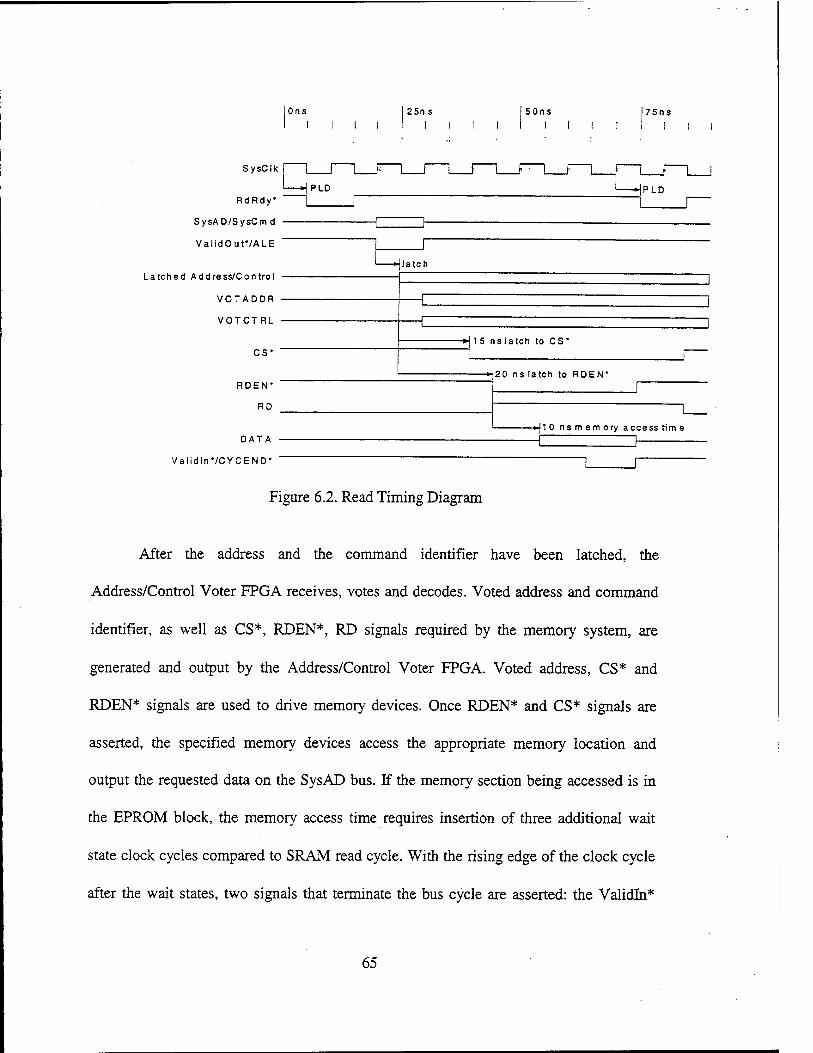
Ons 25n s
I I
50ns 75ns
I I I I I I I I I
SysCIk
RdRdy
SysAD/SysCm d
ValidOut'/ALE
Latched Address/Control
VOTADDR
VOTCTRL
CS'
RDEN*
RD
DATA ■
ValidlnVCYCEND*
PLD -HPLD
-€___>
latch
15 nslatch to CS'
20 ns latch to RDEN'
-*j10 nsmemory access ti me
Figure 6.2. Read Timing Diagram
After the address and the command identifier have been latched, the
Address/Control Voter FPGA receives, votes and decodes. Voted address and command
identifier, as well as CS*, RDEN*, RD signals required by the memory system, are
generated and output by the Address/Control Voter FPGA. Voted address, CS* and
RDEN* signals are used to drive memory devices. Once RDEN* and CS* signals are
asserted, the specified memory devices access the appropriate memory location and
output the requested data on the SysAD bus. If the memory section being accessed is in
the EPROM block, the memory access time requires insertion of three additional wait
state clock cycles compared to SRAM read cycle. With the rising edge of the clock cycle
after the wait states, two signals that terminate the bus cycle are asserted: the Validln*
65

signal, which indicates to the processors that data on SysAD busses from memory is
valid, and the CYCEND* signal, which indicates the end of cycle and de-asserts RDEN*
and CS* signals. After sensing Validln* signal, processors read the data on their SysAD
busses and the read cycle is terminated.
B. WRITE CYCLES
During a write cycle, the processor initiates the bus cycle and issues data to be
written, memory system responds to the request and the bus cycle is terminated. Since
EPROM is a read-only device, write cycle timing analysis was conducted based on only
SRAM device parameters. The write cycle timing diagram is presented in Figure 6.3.
Ons 25ns I I I I I
50ns 75ns
SysClk
WrRdy"
SysAD/SysCmd
ValidOuf/ALE
Latched Address/Control
VOTADDR ■
VOTCTRL -
cs- "
WR/WRDATAEN
VOTDATA -
CYCEND7WREN*
PLD
J I f
Addr/Cntr
J-C
^Latch
vote
ivote
Data
15 ns latch to CS*
I F PLD
-»|20 ns latch to WRDATAEN
-HPLD
Figure 6.3. Write Timing Diagram
66

Once the processors sense the WrRdy* signal which remains asserted unless a
new bus transaction is initiated, they initiate the write bus cycle by driving the SysAD bus
with the address, the SysCmd bus with the command identifier and by asserting the
ValidOut* signal which indicates that valid address and command identifier are driven on
the corresponding busses. The address and the command identifier are latched after
ValidOut* signal is asserted and they continue to the Address/Control Voter FPGA. In
the next clock cycle, latches are blocked by the negation of ValidOut* signal and do not
pass the input signals from the SysAD bus to the output anymore. At this time, SysAD
busses are driven by the processors with data to be written to the memory.
After the address and the command identifier have been latched, the
Address/Control Voter FPGA where they are voted and decoded receives them. Voted
address and command identifier, as well as CS*, WRDATAEN, WR signals required by
the memory system, are generated and output by the Address/Control Voter FPGA. In
addition, data on SysAD bus is received and voted by Data Voter FPGA. Voted data is
output by Data Voter FPGA when output drivers are enabled by the WRDATAEN signal.
Finally, Write Enable signals that enable the memory devices are generated by PLDs at
the end of the cycle when voted data is available at the data inputs of memory devices.
Voted address, voted data, CS* and write enable signals drive the memory devices.
Two signals are asserted at the end of the write cycle: write enable signals and
CYCEND* signal. Once the write enable signals are asserted, the specified memory
devices write data on the SysAD bus to the appropriate memory location. Simultaneously,
67
CYCEND* signal, which indicates the end of bus cycle and de-asserts WRDATAEN and
CS* signals, is asserted and the write cycle terminates.
C. TIMING ANALYSIS
The timing diagrams are based on the data provided by the datasheets of the
components being used. The latches have a typical latch enable to output delay of 4.7-5.6
ns which is approximated to 5 ns in timing diagrams. The PLDs have a delay of 5 ns
which applies to signals generated thereby. The delay of FPGAs depend on the specific
function. The voting function takes between 5-7 ns, address decoding (CS*) and memory
enable (RDEN*, WRDATAEN) functions take 15 and 20 ns, respectively.
For the read cycle, the time between when the memory is enabled and when data
is available is 6 ns for SRAM which is approximated to 10 ns and 45 ns for PROM. The
difference causes 3 additional wait states during PROM memory access. For the write
cycle, the time when data is valid and the memory is write-enabled is 7 ns which is the
setup time. No hold time is necessary.
Looking at the timing diagrams in Figures 6.2 and 6.3 and considering the
allocation of timing to the components, it is concluded that the system works as described
without contention. However, the effect of voting on the bus speed is clearly seen. A
typical single-processor RC4650 system without TMR completes a read cycle in 5 clock
cycles and a write cycle in 4 clock cycles. [Ref. 13] On the other hand, the RC4650 TMR
system completes a read cycle in 7 clock cycles and a write cycle in 6 clock cycles. The
bus speed is reduced by approximately %50 due to voting and other delays of TMR
68

implementation. This performance is considered acceptable when the speed advantage of
COTS microprocessors is taken into account.
This chapter presented the timing analysis conducted using the method of adding
up delays of each functional unit cascaded in the system to determine the overall system
performance. The following chapter concludes this thesis and discusses possible areas for
follow on research.
69

THIS PAGE INTENTIONALLY LEFT BLANK
70

VII. CONCLUSIONS AND FOLLOW-ON RESEARCH
The previous chapters have provided background information about the TMR
concept and presented the work done in this project. This chapter will present the
conclusions drawn from this project and the areas to be worked on for follow-on research.
A. CONCLUSIONS
Due to rapidly shrinking radiation hardened device market and increasing cost of
such devices, the use of COTS devices, which offer state-of-the-art technology, in
radiation environment has been gaining support increasingly. However, the susceptibility
of COTS devices to SEUs requires the implementation of a protection mechanism, one
example of which is the TMR concept used in this project.
The TMR system implemented in this thesis incorporates 64-bit microprocessors
with the intent of increasing the system performance compared to the previously designed
32-bit TMR system of Ref. 2 and Ref. 3 while maintaining the same functionality. Thus,
by the use of COTS devices in space applications, state-of-the-art technology is
introduced. However, the scope of this thesis was limited to a system designed to verify
the possibility of implementing a 64-bit TMR design and to observe the performance
improvement rather than presenting a fully functional fault-tolerant computing unit. So, it
does not include all the functionality of the previous design although it was based on this
previous work.
The system consists of processors, memory system and the programmable glue
logic in between. The processor was selected based on the criteria presented in Chapter
HI. The memory system includes ROM and RAM units. The programmable logic where
71

most of the design work was focused contains the address decoder, voter and memory
control/enable units. The use of 64-bit processors introduced the difficulty of dealing with
increased number of pins and required the use of programmable devices with more I/O
pins to accommodate the functions to be executed on those 64-bit busses. After schematic
designs were drawn and the programmable devices were designed, the timing analysis of
the system was conducted to determine that there were no bus contentions and that the
system functioned äs expected.
The implementation in this research and the work of previous researchers on this
topic prove that the TMR concept is a valid method of protecting against the effects of
SEUs on COTS devices. In addition, this thesis supports the claim that the higher
performance COTS processors can be incorporated into a TMR system to realize the
objective of increasing the system performance while maintaining fault tolerance. The
performance figures in Chapter VI verify this conclusion.
The fact that the performance penalty of TMR implementation is applicable only
during external memory access cycles and not during the internal operation of the
processors, suggests that the performance penalty of TMR implementation can be
tolerated in return for the benefit of fault tolerance gained from the implementation.
B. FOLLOW-ON RESEARCH
Since the scope of the projects as large as this one is too wide to be completed
during the research period of one student, the project needs to be completed by other
students as a result of their follow-on research. The possible areas of follow-on research
are explained in this section.
72
1. Completion of TMR Hardware Implementation
This thesis presented a partial design of a TMR RC4650 system. The current
design includes only the core of a TMR system that consists of the RC4650
microprocessors, the memory system and the programmable logic that performs the
system interface function between the processors and the memory system. This
configuration allows verifying the possibility of implementing a TMR system using 64-
bit microprocessors and evaluating its performance.
In order to provide the full functionality of the system, the design has to be
completed to make it ready to be manufactured on a board. The design and
implementation of a System Controller FPGA, which controls data transfer to the
operating system during an interrupt for analysis, and the associated FIFO array are the
most important features to complete the TMR system. Besides the functional units of the
TMR concept, the support elements are also essential to make the actual hardware work.
They need to be completed before the design can be converted to an actual board. The
support elements include the I/O interface to communicate with peripheral units and to
load programs, the clock circuit, the reset circuit, the interrupt logic and the power/ground
connections.
2. Hardware-Software Integration
Once the hardware design is complete and the board is manufactured and fully
tested, the software necessary to control and operate the system needs to be integrated.
This includes an operating system and a software interface module that is in charge of the
interrupt handling and error recovery process. The software integration section of this
73

project will have similarities with the previous software integration work on the TMR
R3081 design, which was presented in Ref. 4. Thus, this follow-on research may begin by
following the steps taken in the thesis work mentioned above.
3. Radiation Testing
After the hardware and software integration and testing is completed, the system
will be ready for radiation testing. Since the system is designed to detect and correct
radiation induced SEUs, it must be tested in a radiation environment before it can be
declared operational. Radiation testing can be conducted at the test facilities in University
of California, Berkeley and University of California, Davis. The influence of SEUs on the
system can be analyzed by using the data captured by the software interface module that
will be developed during software integration.
In addition, the system can be used to compare TMR hardware fault tolerance
technique with software fault tolerance techniques. This requires conducting tests in TMR
mode and single processor mode since the system can operate in either of those modes.
74

APPENDIX A. TMR DESIGN SCHEMATICS
This appendix presents the schematics for the TMR RC4650 System. Table A.l
lists the schematics and the pages they appear on.
Figure Number and Description Page Number
Figure A. 1. TMR RC4650 Top Level Schematic 76
Figure A.2. One of the three microprocessors and the associated latches 77
Figure A.3. Address/Control Voter FPGA with PLD1 and PLD2 78
Figure A.4. Data Voter FPGA 79
Figure A.5. PROM Memory Block 80
Figure A.6 KRAM and SRAMO Segments of SRAM Memory Block 81
Figure A.7 SRAM1 and SRAM2 Segments of SRAM Memory Block 82
Figure A. 8 SRAM3 Segment of SRAM Memory Block 83
75
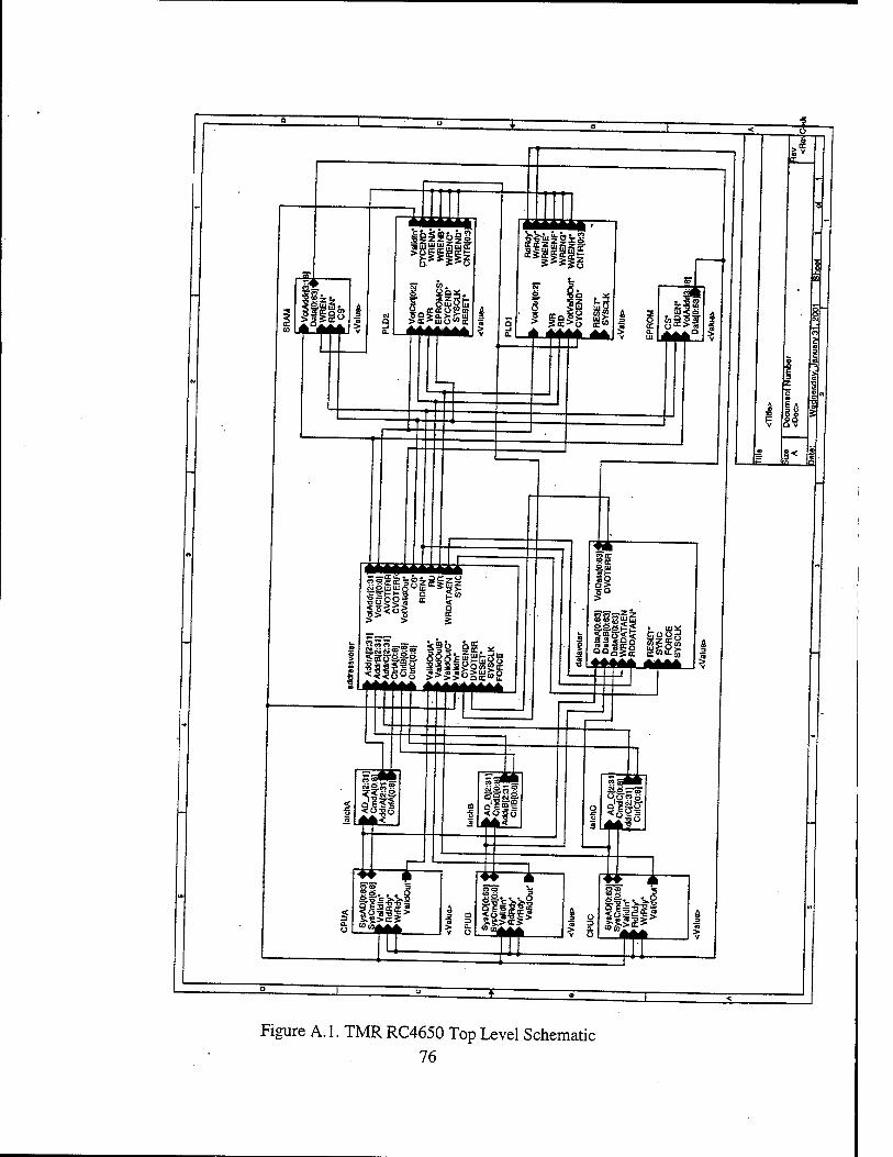
Figure A.l. TMR RC4650 Top Level Schematic 76

iiiüiii Hi iliii iiiiilli iiilill
Figure A.2. One of the three microprocessors and the associated latches
77
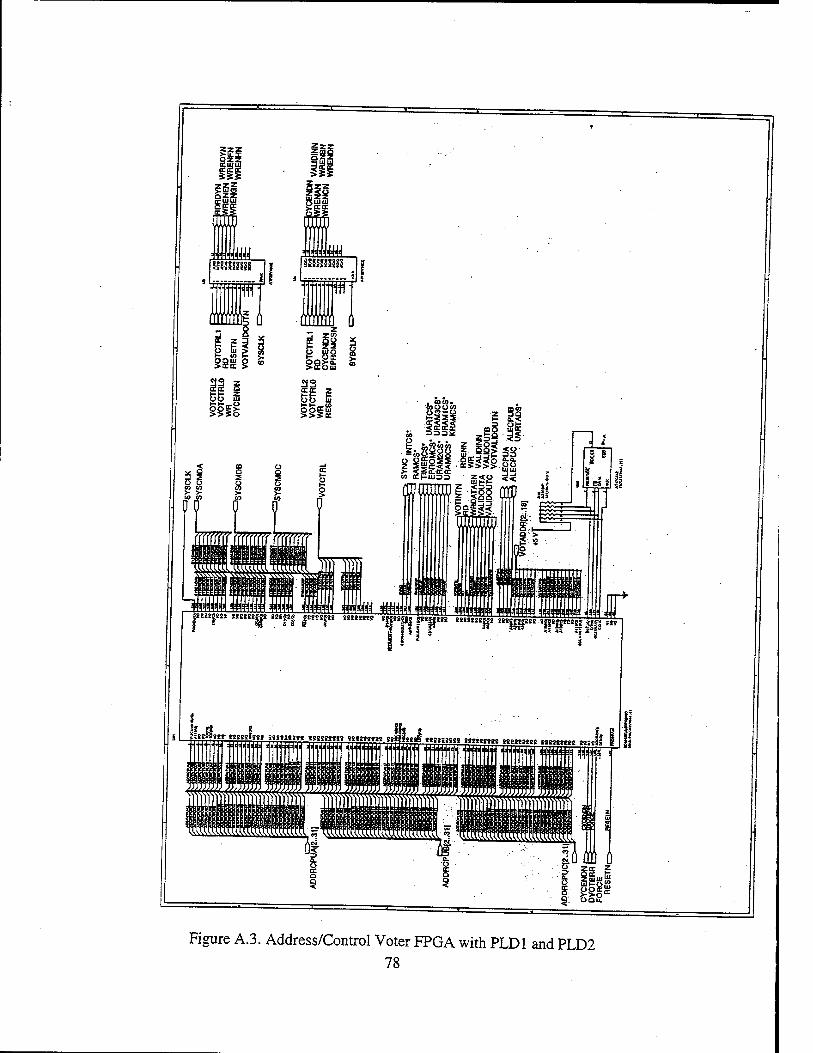
I
Figure A.3. Address/Control Voter FPGA with PLD1 and PLD2 78
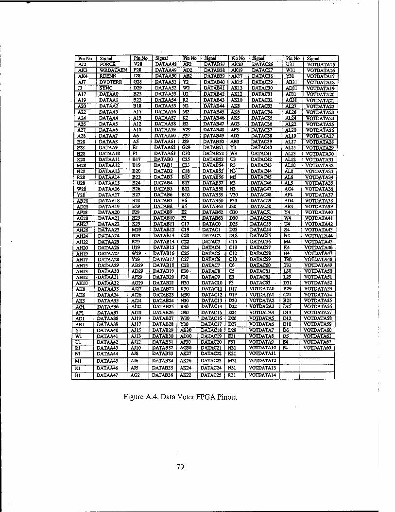
Pin No Signal Pin No Signal Pin No Siaial Pin No Signal Pin No Signal AJ2 FORCE V28 DATAA48 AF2 DATAB37 AK20 DATAC26 U31 VOTDATA15 AK3 WRDATAEN P28 DATAA49 AD2 DATAB38 AK19 DATAC27 W31 VOTDATA16 AK4 RDENN J28 DATAA50 AB2 DATAB39 AK17 DATAC28 Y31 VOTDATA17 AI7 DVOTERR G28 DATAA51 Y2 DATAB40 AK15 DATAC29 AB31 VOTDATA18 J3 SYNC D29 DATAAS2 W2 DATAB41 AK13 DATAC30 AD31 VOTDATA19 A17 DATAAO B25 DATAA53 U2 DATAB42 AK12 DATAC31 AF31 VOTDATA20 A19 DATAA1 B23 DATAA54 R2 DATAB43 AK10 DATAC32 AG31 VOTDATA21 A20 DATAA2 B18 DATAASS N2 DATAB44 AK8 DATAC33 AL27 VOTDATA22 A22 DATAA3 A15 DATAA56 M2 DATAB45 AKfi DATAC34 AL26 VOTDATA23 A24 DATAA4 A13 DATAA57 K2 DATAB46 AK5 DATAC35 AL24 VOTDATA24 A26 DATAA5 A12 DATAA58 H2 DATAB47 AG3 DATAC36 AL22 VOTDATA25 A27 DATAA6 A10 DATAA59 V29 DATAB48 AF3 DATAC37 AL20 VOTDATA26 A28 DATAA7 A6 DATAA60 P29 DATAB49 AD3 DATAC38 AL19 VOTDATA27 E28 DATAA8 A5 DATAA61 J29 DATAB50 AB3 DATAC39 AU7 VOTDATA28 F28 DATAA9 El DATAA62 G29 DATAB51 Y3 DATAC40 AL15 VOTDATA29 H28 DATAA10 Fl DATAA63 C30 DATAB52 W3 DATAC4I AU3 VOTDATA30 K28 DATAA11 B17 DATABO C25 DATAB53 U3 DATAC42 AL12 VOTDATA31 M28 DATAA12 B19 DATAB1 C23 DATAB54 R3 DATAC43 AUO VOTDATA32 N2S DATAA13 B20 DATAB2 C18 DATAB55 N3 DATAC44 AJL8 VOTDATA33 R28 DATAA14 B22 DATAB3 B15 DATAB56 M3 DATAC45 AL6 VOTDATA34 U28 DATAA1S B24 DATAB4 B13 DATAB57 K3 DATAC46 ALS VOTDATA35 W28 DATAA16 B26 DATAB5 B12 DATABS8 H3 DATAC47 AG4 VOTDATA36 Y28 DATAA17 B27 DATAB6 BIO DATAB59 V30 DATAC48 AF4 VOTDATA37 AB28 DATAA18 B28 DATAB7 B6 DATAB60 P30 DATAC49 AD4 VOTDATA38 AD28 DATAA19 E29 DATAB8 BS DATAB61 J30 DATAC50 AB4 VOTDATA39 AF28 DATAA20 F29 DATAB9 E2 DATABÖ2 G30 DATAC5L Y4 VOTDATA40 AG28 DATAA21 K29 DATABIO F2 DATAB63 D30 DATAC52 W4 VOTDATA41 AH27 DATAA22 K29 DATAB11 C17 DATACO D25 DATAC53 U4 VOTDATA42 AH26 DATAA23 M29 DATAB12 C19 DATAC1 D23 DATAC54 R4 VOTDATA43 AH24 DATAA24 N29 DATAB13 C20 DATAC2 D18 DATAC55 N4 VOTDATA44 AH22 DATAA25 R29 DATAB14 C22 DATAC3 C15 DATAC56 M4 VOTDATA4S AH20 DATAA26 U29 DATAB15 C24 DATAC4 C13 DATAC57 E4 I VOTDATA46 AH19 DATAA27 W29 DATAB16 C26 DATAC5 C12 DATAC58 H4 VOTDATA47 AH17 DATAA28 Y29 DATAB17 C27 DATAC6 CIO DATACS9 T30 VOTDATA48 AH15 DATAA29 AB29 DATAB18 C28 DATAC7 C6 DATAC60 T31 VOTDATA49 AHI3 DATAA30 AD29 DATAB19 E30 DATAC8 C5 DATAC61 130 VOTDATA50 AH12 DATAA31 AF29 DATAB20 F30 DATAC9 E3 DATAC62 139 VOTDATA51 AH10 DATAA32 AG29 DATAB21 H30 DATACIO F3 DATAC63 D31 VOTDATA52 AH8 DATAA33 AJ27 DATAB22 K30 DATAC11 D17 VOTDATAO B29 VOTDATA53 AH6 DATAA34 AJ26 DATAB23 M30 DATAC12 D19 VOTDATA1 C21 VOTDATA54
AH5 DATAA35 AJ24 DATAB24 N30 DATAC13 D20 VOTDATA2 B21 VOTDATA55 AG1 DATAA36 AJ22 DATAB25 R30 DATACI4 D22 VOTDATA3 DI5 VOTDATA56 AF1 DATAA37 AJ20 DATAB26 U30 DATAC15 D24 VOTDATA4 D13 VOTDATA57 AD1 DATAA38 AJ19 DATAB27 W30 DATAC16 D26 VOTDATA5 DI2 VOTDATA58 AB1 DATAA39 AJ17 DATAB28 Y30 DATAC17 D27 VOTDATA6 D10 VOTDATA59 Yl DATAA40 AJ15 DATAB29 AB30 DATACI8 D28 VOTDATA7 D6 VOTDATA60 WI DATAA41 AJ13 DATAB30 AD30 DATACI9 E31.. VOTDATA8 D5 VOTDATA61 Ul DATAA42 AJ12 DATAB31 AF30 DATAC20 P31 VOTDATA9 E4 VOTDATA62 Rl DATAA43 AJIO DATAB32 AG30 DATAC21 H31 VOTOATA10 F4 VOTDATA63 Nl DATAA44 AJ8 DATAB33 AK27 DATAC22 K31 VOTDATAll
Ml DATAA45 AJ6 DATAB34 AK26 DATAC23 M31 V0fTOATA12
KI DATAA46 AJ5 DATAB35 AK24 DATAC24 N31 VOTDATA13
HI DATAA47 AG2 DATAB36 AK22 DATAC25 R31 VOTDATA14
Figure A.4. Data Voter FPGA Pinout
79
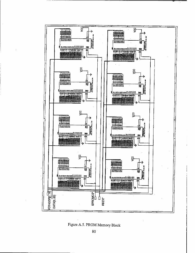
aisssis
15355551
! ?<35I3I5?l555;35=
KEEEEEKKEKE
H IS t
2 5 SfefeÖ&fel
85555555
«sa«ss««<;iss B»
SSSSSSSS 1115533 5S sppss
„,,iü:.::i."i 4-
sssssss §3555155 aiiiissB
o o- >
Isä5ä55i §
i SI3333J5 **<<<<i<
ggfiEEEEECKEKE 21
■<< ISO 5s
4>
CO Ü 5 O az a. UJ
Öü UJ Q EC
SSSSSSSS 35351:!; ajäpppjin
§1555556
EiEEEEpra
D ftüö i
SSSSSS'
IssJis
25SS555S
jiajjasss?;
ggEEEE'KKEEEE s;-Koiaiibst:itn
'S/'rS^jr/-/-S'S-S-/-S-y-, H>
O o. ■SSSSSSS
s i 51 • i ;
rHl"
isSs521S I lim EigCECiCDI iic-i..'.i,,t._iit^ii
"sT 'W^s 5535*5} Ipgfsg i i i
ss«:
5si55§5e
I EfüEEEEEKKKE
Figure A.5. PROM Memory Block
80
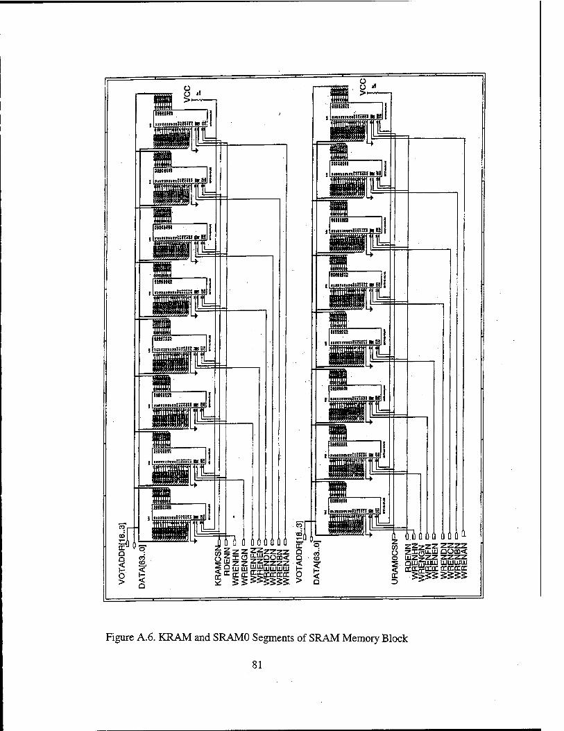
«E-0 Q D < o >
5ÄZ2ggzzzz < ^ 2 E tr cc EEtnrcca: O 5
i 6üö06 0000- OT ZZzZZZZZZ O UJZ^ZZZZZZ
< cccnScca: OCXECCC
Figure A.6. KRAM and SRAMO Segments of SRAM Memory Block
81
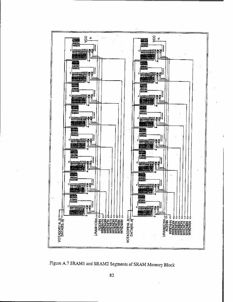
mm» miiiiM.nm» m SS
MHHI
HfHHJ
wmi»«HS5» m t!
«Uflll
«HU»
mnroiiliWil ■ H
HIHHI
taft»iw—Si3s5t; IB Bi
1HKIB
tttnxnnHBHI B H
ü1 w«iy*»t»näaä3? Me 2J
Ihi öö Ö
i—CO
o >
m ZZZ22Z2ZZ « O £! UJZZZZZZZZ ? 23 ^ QLUUltULULLILUUJai £■£.
O >
Figure A.7 SRAM1 and SRAM2 Segments of SRAM Memory Block
82
OZXCj£ujQÜ0Q< 2UJZZZ2ZZZZ SQiiiujuJUJUJUJiULU garcoimrcccccca:
Figure A.8 SRAM3 Segment of SRAM Memory Block
83

THIS PAGE INTENTIONALLY LEFT BLANK
84

APPENDIX B. PROGRAMMABLE LOGIC DESIGN EQUATIONS
When programming the programmable devices such as PLDs and FPGAs,
equations must be written that define the signals to be generated when input signals are
applied to the devices. The PLD programming equations are based on paper design rather
than actually being compiled and simulated. However, the FPGA programming equations
were compiled and simulated using the Xilinx Foundation Series Design Suite. Section 1
contains the programming equations for PLDs and Section 2 contains the programming
equations for the Address/Control Voter FPGA.
In the following equations, a dot (.) means a logical AND operation, a plus (+)
means a logical OR operation and an exclamation mark (!) means a logical NOT
operation.
1. PLD Programming Equations
RdRdy* = CYCEND* . RdRdy* + IValidOut*
WrRdy* = CYCEND* . WrRdy* + JValidOut*
CYCEND* = !(RESET* . (RD . CNTR==7 + IEPROMCS* . RD . CNTR=10
WR . CNTR==6 + CNTR==F))
Validln* = !(RESET* . (RD . CNTR==7 + IEPROMCS* . RD . CNTR=10))
WRENA* = !(RESET* . WR . CNTR=6)
WRENB* = !(RESET* . (VOTCTRL2 + VOTCTRL1 + VOTCTRLO) . WR .
CNTR==6)
WRENC* = !(RESET* . (VOTCTRL2 + VOTCTRL1). WR . CNTR=6)
85
WREND* = .'(RESET* . (V0TCTRL2 + V0TCTRL1 . VOTCTRLO) . WR
CNTR==6)
WRENE* = !(RESET* . VOTCTRL2 . WR . CNTR=6)
WRENF* = !(RESET* . ( .'VOTCTRL2 + 1VOTCTRL1 . IVOTCTRLO ). WR
CNTR==6)
WRENG* = !(RESET* . (IVOTCTRL2 + JVOTCTRL1). WR . CNTR==6)
WRENH* = !(RESET* . ( !VOTCTRL2 + IVOTCTRL1 + IVOTCTRLO). WR .
CNTR=6)
2. FPGA Programming Equations
RD = .'VOTCTRL7. IVOTCTRL6 . IVOTCTRL5
WR = IVOTCTRL7 . VOTCTRL6 . IVOTCTRL5
RDEN* = !(RESET* . CYCEND* . IVOTCTRL7 . IVOTCTRL6 . 1VOTCTRL5)
WRDATAEN* = RESET* . CYCEND* . VOTCTRL8 . IVOTCTRL7
JVOTCTRL6. IVOTCTRL5
86

APPENDIX C. XILINX FOUNDATION SERIES FPGA DESIGN
The FPGAs also need to be programmed just like the PLDs. However, schematic
diagrams were used to program the FPGAs instead of writing the programming code in
ABEL or Verilog because the Xilinx Foundation Series FPGA design tool offered
schematic programming of the FPGAs. The designer can enter the design in schematic
format and the tool converts it to a netlist and compiles to get the FPGA programming
code. Section 1 of this appendix presents the schematics for the Address/Control Voter
FPGA and Section 2 presents the schematics for the Data Voter FPGA.
1. Address/Control Voter FPGA
The design schematics of the Address/Control Voter FPGA are presented in the
following figures and Table C.l lists the figures and the pages they appear on.
Figure Number and Description Page
Figure C.l. Address Voter/Memory Decoder Section of Address/Control Voter
FPGA
88
Figure C.2. Control Voter Section of Address/Control Voter FPGA 89
Figure C.3. Memory Interface Section of Address/Control Voter FPGA 90
Figure C.4. 4-bit Wide Majority Voter Macro (VOTER4) 91
Figure C.5. One 30-bit Address Bus Input Macro 92
Figure C.6 Voted Address Bus Output Macro 93
Figure C.7 9-bit Wide Majority Voter Macro (VOTER9) 94
Figure C.8 9-bit System Command (Control) Bus Input Macro 95
87
Figure C.l. Address Voter/Memory Decoder Section of Address/Control Voter FPGA 88

ti
Figure C.2. Control Voter Section of Address/Control Voter FPGA
89
A«
a a
P
8 8 S
If <v Cp[ £
9
A* A«
A«
rp*
a a I- H od i-t- oo >>
A»
AJ
_ ou
>>>
a a i-1-
V y u
a do ü
cu
l-l-l—l-l- ooooo öd i-(-1-1-1- ooooo
Figure C.3. Memory Interface Section of Address/Control Voter FPGA 90
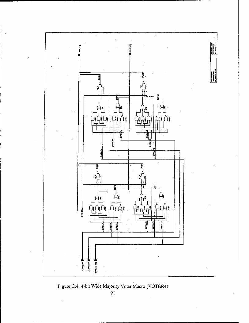
m
Figure C.4. 4-bit Wide Majority Voter Macro (VOTER4) 91
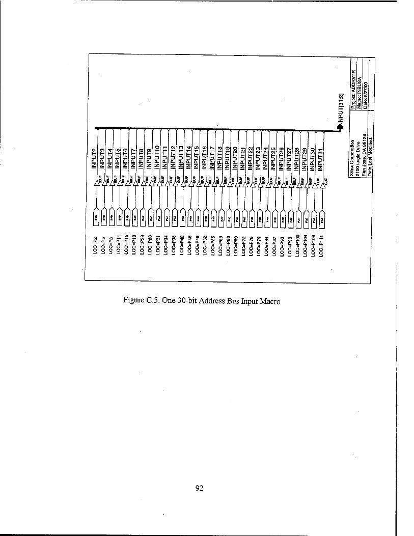
CM
£2. h- O Q. Z.
vvvvvvvvvv y y V V TT
Mffl™™™^
CM « ■*■ w eg CM CM CM l- 3 5 •=> Q. Q. Q. Q. Z Z 7 7" _ IL u. IL „ riJ äf tdy \ri A
Oi
!Q<
O _j o
= * = X W CO
-. .«. — T-loco n <o ^ ^ a) N 0- 0.0.0.0.0.0.0.0.0.0.0.
.« A A A JJ » » II ii M " ? 2 S ? ? ? ß ß 5 S 8 8 I I § =
§s§i§ilii§ll§llillilliiiglllll
Figure C.5. One 30-bit Address Bus Input Macro
92

01 Ö) o> o> O)
B. a. o. Q. 8 o. £ 2! £ _
ii ii ii ii n n ii II ii ii
88888 8 8888 i i i i i i i
o u o S-& -
r? ™ 2 U _j o 2 9 "*
X CM CO
AAAAAAAAAAAA
<M
Q. ■I- D O
Figure C.6 Voted Address Bus Output Macro
93

Figure C.7 9-bit Wide Majority Voter Macro (VOTER9) 94

o £. < 3 Q. O _1 tr O
/ / /
o ,_ w CO ■<t IT) < < < < < < -> 3 D 3 3 3 a. a. a. a. a. a. o o o o ü q _i _i _j _i _J -i IZ n: a: DC EC DC t- t- i- H 1- H o o o O O O
/ J5/ u. u.
\1J u.
A A
Ü
y \
•
o *■■ oa s 3 in CD <*• CO m CD m m m m m 3 3 3 3 3 3 3 3 3 Q. Q. a. a. a. a. a. a. 0. O O o (> O (> o o O _l _J _i _J _i -i -i _J _l QC DC oc DC DC QC DC a. DC 1- 1- H t- f- H t- ^- 1- Ü o ü Ü Ü O O o o
/ y»/
u.
A) U. U. u.
M} Ji/1 \*/
u.
© 2. 5 3 a. o
!
a. a. a. a.
St- CM
■■ « « a. a. o o O Q 88 8
u> <c* r»
a. a. a. a. a.
8-8
) ) ^ •
o ^ CM CO s w CO 1^ on Ü O O O O C) O O 3 3 3 3 ■3 3 3 3 3 a. a. a. 0. a. a. a. a. a. o o O o o O o O o _i _j _i -1 _i _j _i -i _i DC DC DC DC DC DC oc oc (t h- ■(- t- y- h- H H- 1- i- Ü Ü Ü o Ü Ü Ü o o
} U.
J J \»/ JIJ vi/ £/ J/ ̂ i/ jg
© CO
Ü 3 a. o
f S 5 <
|f S X Q ">
o.. a. a. ii a ii o o O O O O
a. a. a. a.
Figure C.8 9-bit System Command (Control) Bus Input Macro
95
2. Data Voter FPGA
The design schematics of the Data Voter FPGA are presented in the following
figures and Table C.2 lists the figures and the pages they appear on.
Figure Number and Description Page
Figure C.9. Top Level Schematic of Data Voter FPGA 97
Figure C. 10. One 64-bit Data Bus Input Macro 98
Figure C. 11. 64-bit Voted Data Bus Output Macro 99
Figure C. 12. 16-bit Wide Majority Voter Macro (VOTER16) 100
96
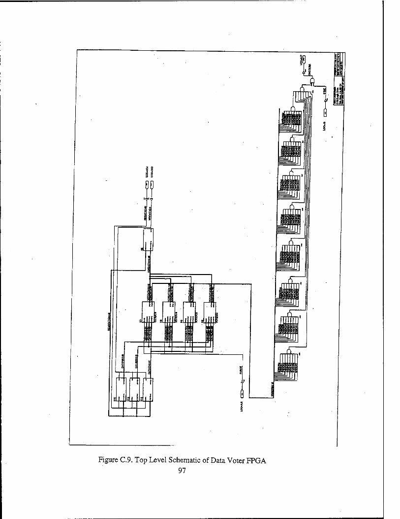
Figure C.9. Top Level Schematic of Data Voter FPGA 97
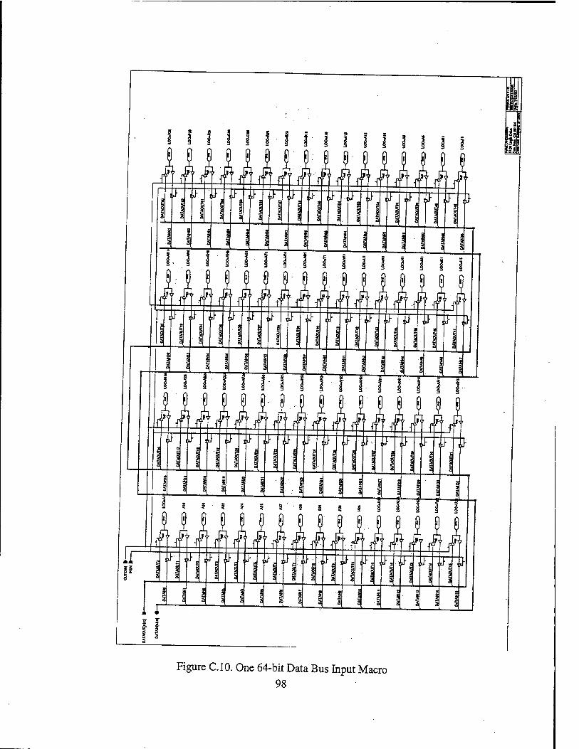
Figure CIO. One 64-bit Data Bus Input Macro 98
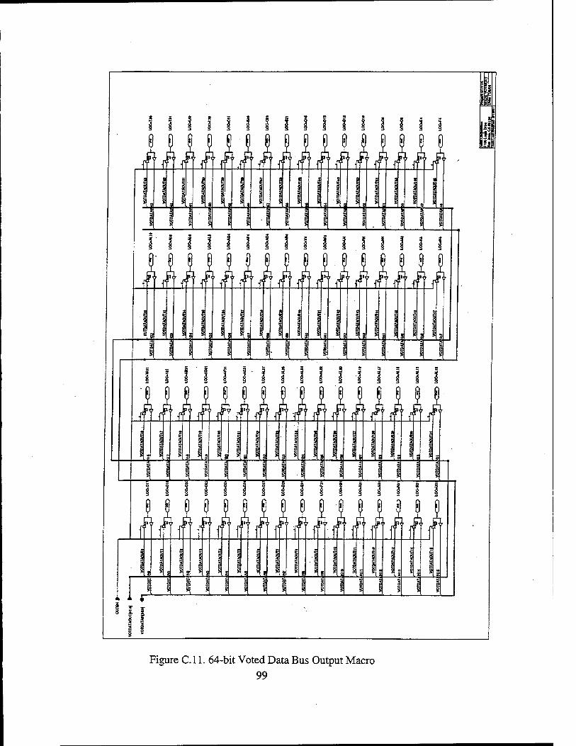
Figure C.l 1. 64-bit Voted Data Bus Output Macro 99
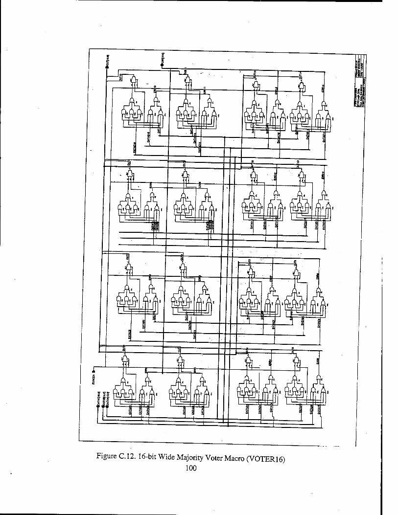
—C -M J ' m
i
Figure C.12. 16-bit Wide Majority Voter Macro (VOTER16) 100

LIST OF REFERENCES
1. Payne, Jr., J. C, "Fault Tolerant Computing Testbed: A Tool for the Analysis of Hardware and Software Fault Handling Techniques," Master's Thesis, Naval Postgraduate School, Monterey, CA, December 1998.
2. Summers, David., "Implementation of a Fault Tolerant Computing Testbed: A tool for the analysis of hardware and software fault handling techniques," Master's Thesis, Naval Postgraduate School, Monterey, CA, June 2000.
3. Hofheinz, Damen, "Completion and Testing of a TMR Computing Testbed and Recommendation for a Flight-Ready Follow-On Design," Master's Thesis, Naval Postgraduate School, Monterey, CA, December 2000.
4. Groening, S. E., and Whitehouse, K. D., "Application of Fault-Tolerant Computing for Spacecraft Using Commercial-Off-The-Shelf Microprocessors," Master's Thesis, Naval Postgraduate School, Monterey, CA, June 2000.
5. National Semiconductor, Radiation Owner's Manual, National Semiconductor, 1999.
6. Weste, N. H. E. and Eshraghian, K., Principals of CMOS VLSI Design: A Systems Perspective, 2nd Edition, Addison-Wesley, Menlo Park, CA, 1994.
7. Asenek, V., et al., "SEU Induced Errors Observed in Microprocessor Systems," IEEE Transactions on Nuclear Science, Vol. 45, No. 6, December 1998. pp 2876- 2883.
8. Underwood, C. I. and Oldfield, M. K., "Observed Radiation-Induced Degradation of Commercial-Off-The-Shelf (COTS) Devices Operating in Low-Earth Orbit," IEEE Transactions on Nuclear Science, Vol. 45, No. 6, December 1998. pp 2737- 2744.
9. Savio, Chau. "Experience of using COTS Components for Deep Space Missions," Proceedings, 4th IEEE International Symposium on High-Assurance Systems Engineering, 1999.
10. Johansson, R., "Two Error-Detecting and Correcting Circuits for Space Applications," Proceedings of Annual Symposium on Fault Tolerant Computing, 1996. pp 436-439.
11. Johnson, B.W., Design and Analysis of Fault Tolerant Digital Systems, Addison- Wesley, New York, NY, 1989.
101

12. Integrated Device Technology, Inc., The IDT79R3071. IDT79R3081 RISController Hardware User's Manual. Revision 2. Santa Clara, CA, 1994.
13. Integrated Device Technology, Inc., The IDT79RC4630/IDT79RC4650 RISC Processor Hardware User's Manual. Version 2.1. Santa Clara, CA, August 1998.
14. XILINX, The Programmable Logic Data Book. 1999.
102
INITIAL DISTRIBUTION LIST
1. Defense Technical Information Center 2 8275 John J. Kingman Road, Suite 0944 Ft. Belvoir, VA 22060-6218
2. Dudley Knox Library 2 Naval Postgraduate School 411 Dyer Road Monterey, CA 93943-5101
3. Chairman, Code EC 1 Department of Electrical and Computer Engineering Naval Postgraduate School Monterey, CA 93943-5121
4. Professor Herschel H. Loomis Code EC/Lm. 2 Department of Electrical and Computer Engineering Naval Postgraduate School Monterey, CA 93943-5121
5. Professor Alan A. Ross Code SP/Ra 2 Space Systems Academic Group Naval Postgraduate School Monterey, CA 93943-5110
6. Engineering and Technology Curricular Office, Code 34 1 Naval Postgraduate School Monterey, CA 93943-5109
7. Ltjg. Huseyin Baha Eken, Turkish Navy 1 Millet Cad. Intibah Sok. Guner Ap. D: 11 42040 Konya-Turkey
8. Deniz Kuvvetleri Komutanligi 1 Bakanliklar-Ankara Turkey
103
Related Documents


